EP2490331A1 - Differential amplifying apparatus - Google Patents
Differential amplifying apparatus Download PDFInfo
- Publication number
- EP2490331A1 EP2490331A1 EP12152605A EP12152605A EP2490331A1 EP 2490331 A1 EP2490331 A1 EP 2490331A1 EP 12152605 A EP12152605 A EP 12152605A EP 12152605 A EP12152605 A EP 12152605A EP 2490331 A1 EP2490331 A1 EP 2490331A1
- Authority
- EP
- European Patent Office
- Prior art keywords
- signal
- terminal
- input
- output
- differential amplifier
- Prior art date
- Legal status (The legal status is an assumption and is not a legal conclusion. Google has not performed a legal analysis and makes no representation as to the accuracy of the status listed.)
- Withdrawn
Links
- 239000003990 capacitor Substances 0.000 claims abstract description 13
- YCLAMANSVUJYPT-UHFFFAOYSA-L aluminum chloride hydroxide hydrate Chemical compound O.[OH-].[Al+3].[Cl-] YCLAMANSVUJYPT-UHFFFAOYSA-L 0.000 description 20
- 238000010586 diagram Methods 0.000 description 5
- 230000003321 amplification Effects 0.000 description 2
- 238000000034 method Methods 0.000 description 2
- 238000003199 nucleic acid amplification method Methods 0.000 description 2
- 230000008878 coupling Effects 0.000 description 1
- 238000010168 coupling process Methods 0.000 description 1
- 238000005859 coupling reaction Methods 0.000 description 1
- 238000012986 modification Methods 0.000 description 1
- 230000004048 modification Effects 0.000 description 1
- 230000000737 periodic effect Effects 0.000 description 1
Images
Classifications
-
- H—ELECTRICITY
- H03—ELECTRONIC CIRCUITRY
- H03F—AMPLIFIERS
- H03F3/00—Amplifiers with only discharge tubes or only semiconductor devices as amplifying elements
- H03F3/34—DC amplifiers in which all stages are DC-coupled
-
- H—ELECTRICITY
- H03—ELECTRONIC CIRCUITRY
- H03F—AMPLIFIERS
- H03F3/00—Amplifiers with only discharge tubes or only semiconductor devices as amplifying elements
- H03F3/45—Differential amplifiers
- H03F3/45071—Differential amplifiers with semiconductor devices only
- H03F3/45479—Differential amplifiers with semiconductor devices only characterised by the way of common mode signal rejection
- H03F3/45928—Differential amplifiers with semiconductor devices only characterised by the way of common mode signal rejection using IC blocks as the active amplifying circuit
- H03F3/45932—Differential amplifiers with semiconductor devices only characterised by the way of common mode signal rejection using IC blocks as the active amplifying circuit by using feedback means
-
- H—ELECTRICITY
- H03—ELECTRONIC CIRCUITRY
- H03F—AMPLIFIERS
- H03F3/00—Amplifiers with only discharge tubes or only semiconductor devices as amplifying elements
- H03F3/45—Differential amplifiers
- H03F3/45071—Differential amplifiers with semiconductor devices only
- H03F3/45076—Differential amplifiers with semiconductor devices only characterised by the way of implementation of the active amplifying circuit in the differential amplifier
- H03F3/45475—Differential amplifiers with semiconductor devices only characterised by the way of implementation of the active amplifying circuit in the differential amplifier using IC blocks as the active amplifying circuit
-
- H—ELECTRICITY
- H03—ELECTRONIC CIRCUITRY
- H03F—AMPLIFIERS
- H03F3/00—Amplifiers with only discharge tubes or only semiconductor devices as amplifying elements
- H03F3/45—Differential amplifiers
- H03F3/45071—Differential amplifiers with semiconductor devices only
- H03F3/45479—Differential amplifiers with semiconductor devices only characterised by the way of common mode signal rejection
- H03F3/45928—Differential amplifiers with semiconductor devices only characterised by the way of common mode signal rejection using IC blocks as the active amplifying circuit
- H03F3/45932—Differential amplifiers with semiconductor devices only characterised by the way of common mode signal rejection using IC blocks as the active amplifying circuit by using feedback means
- H03F3/45937—Measuring at the loading circuit of the differential amplifier
-
- H—ELECTRICITY
- H03—ELECTRONIC CIRCUITRY
- H03K—PULSE TECHNIQUE
- H03K5/00—Manipulating of pulses not covered by one of the other main groups of this subclass
- H03K5/01—Shaping pulses
- H03K5/08—Shaping pulses by limiting; by thresholding; by slicing, i.e. combined limiting and thresholding
-
- H—ELECTRICITY
- H03—ELECTRONIC CIRCUITRY
- H03M—CODING; DECODING; CODE CONVERSION IN GENERAL
- H03M1/00—Analogue/digital conversion; Digital/analogue conversion
- H03M1/66—Digital/analogue converters
-
- H—ELECTRICITY
- H03—ELECTRONIC CIRCUITRY
- H03F—AMPLIFIERS
- H03F2200/00—Indexing scheme relating to amplifiers
- H03F2200/331—Sigma delta modulation being used in an amplifying circuit
-
- H—ELECTRICITY
- H03—ELECTRONIC CIRCUITRY
- H03F—AMPLIFIERS
- H03F2203/00—Indexing scheme relating to amplifiers with only discharge tubes or only semiconductor devices as amplifying elements covered by H03F3/00
- H03F2203/45—Indexing scheme relating to differential amplifiers
- H03F2203/45424—Indexing scheme relating to differential amplifiers the CMCL comprising a comparator circuit
-
- H—ELECTRICITY
- H03—ELECTRONIC CIRCUITRY
- H03F—AMPLIFIERS
- H03F2203/00—Indexing scheme relating to amplifiers with only discharge tubes or only semiconductor devices as amplifying elements covered by H03F3/00
- H03F2203/45—Indexing scheme relating to differential amplifiers
- H03F2203/45438—Indexing scheme relating to differential amplifiers the CMCL uses digital signals
-
- H—ELECTRICITY
- H03—ELECTRONIC CIRCUITRY
- H03F—AMPLIFIERS
- H03F2203/00—Indexing scheme relating to amplifiers with only discharge tubes or only semiconductor devices as amplifying elements covered by H03F3/00
- H03F2203/45—Indexing scheme relating to differential amplifiers
- H03F2203/45544—Indexing scheme relating to differential amplifiers the IC comprising one or more capacitors, e.g. coupling capacitors
-
- H—ELECTRICITY
- H03—ELECTRONIC CIRCUITRY
- H03F—AMPLIFIERS
- H03F2203/00—Indexing scheme relating to amplifiers with only discharge tubes or only semiconductor devices as amplifying elements covered by H03F3/00
- H03F2203/45—Indexing scheme relating to differential amplifiers
- H03F2203/45594—Indexing scheme relating to differential amplifiers the IC comprising one or more resistors, which are not biasing resistor
-
- H—ELECTRICITY
- H03—ELECTRONIC CIRCUITRY
- H03F—AMPLIFIERS
- H03F2203/00—Indexing scheme relating to amplifiers with only discharge tubes or only semiconductor devices as amplifying elements covered by H03F3/00
- H03F2203/45—Indexing scheme relating to differential amplifiers
- H03F2203/45604—Indexing scheme relating to differential amplifiers the IC comprising a input shunting resistor
-
- H—ELECTRICITY
- H03—ELECTRONIC CIRCUITRY
- H03F—AMPLIFIERS
- H03F2203/00—Indexing scheme relating to amplifiers with only discharge tubes or only semiconductor devices as amplifying elements covered by H03F3/00
- H03F2203/45—Indexing scheme relating to differential amplifiers
- H03F2203/45618—Indexing scheme relating to differential amplifiers the IC comprising only one switch
Definitions
- the present invention relates to a differential amplifying apparatus and, more particularly, to correction of the offset voltage of a differential amplifying apparatus.
- a delta-sigma ( ⁇ ) A/D converter is known as a type of analog to digital (A/D) converters.
- a signal having a direct-current (DC) component is input to a low-order ⁇ A/D converter with a simple configuration, a signal having periodicity is superimposed on the digital signal output from the ⁇ A/D converter.
- This periodic signal serves as "tonal noise” with a frequency changing depending on the magnitude of the DC component, and remarkably degrades the signal-to-noise (S/N) ratio.
- the DC component of the signal to be input to the ⁇ A/D converter is made sufficiently small to lower the frequency of the "tonal noise" below the frequency band to be used.
- the offset voltage output from the differential amplifier needs to be suppressed.
- Japanese Patent Laid-Open No. 2006-311350 Japanese Patent Laid-Open No. 2006-311350 (literature 1) is usable.
- the offset corrector described in the literature 1 corrects the output offset voltage of a differential amplifier based on the voltage output from the differential amplifier when the inverting terminal and the non-inverting terminal of the differential amplifier are short-circuited by a switch without any feedback from the output to the input. That is, during the offset voltage correction period, the differential amplifier is operated while short-circuiting its two input terminals, and the offset is corrected based on the output voltage at that time. This operation enables to reduce the output offset voltage of the differential amplifier.
- the two input terminals of the differential amplifier are disconnected by the switch.
- the differential amplifier amplifies the difference signal between the input signals of the two input terminals and outputs the amplified signal. That is, the offset voltage between the input signals of the two input terminals cannot be corrected during the normal operation period. In other words, during the normal operation period, the offset voltage between the input signals of the two input terminals is amplified and therefore cannot be sufficiently corrected.
- the present invention in its first aspect provides a differential amplifying apparatus as specified in claims 1 to 9.
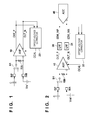
- Fig. 1 is a block diagram for explaining the arrangement of a differential amplifying apparatus according to the first embodiment.
- Fig. 2 is a block diagram for explaining another arrangement of the differential amplifying apparatus.
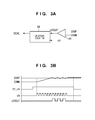
- Figs. 3A and 3B are views for explaining the arrangement and operation of an offset voltage corrector.
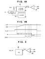
- Figs. 4A and 4B are views for explaining another arrangement and operation of the offset voltage corrector.
- Fig. 5 is a block diagram for explaining still another arrangement of the offset voltage corrector.
- a switch S1 and an input resistance RIN are connected to the first input terminal (non-inverting terminal; to be referred to as a +IN terminal hereinafter) of a differential amplifier 10 shown in Fig. 1 .
- the switch S1 connects/disconnects the +IN terminal to/from a signal input terminal (to be referred to as an INP terminal hereinafter).
- a signal input terminal (to be referred to as an INN terminal hereinafter) and the input resistance RIN are connected to the second input terminal (inverting terminal; to be referred to as a -IN terminal hereinafter) of the differential amplifier 10. That is, the +IN terminal and the -IN terminal are connected via the input resistance RIN.
- the resistance value of the input resistance RIN is much smaller than an input resistance value R +IN , of the +IN terminal and an input resistance value R -IN of the -IN terminal of the differential amplifier 10 (R -IN' R +IN >> RIN).
- the differential amplifier 10 has a first output terminal (positive output terminal; to be referred to as an OUT_P terminal hereinafter) and a second output terminal (negative output terminal; to be referred to as an OUT_N terminal hereinafter) that outputs the inverted signal of the signal of the OUT_P terminal.
- the input terminals of an offset voltage corrector 20 are connected to the OUT_P terminal and the OUT_N terminal, respectively.
- An output OCAL of the offset voltage corrector 20 is connected to the offset correction input terminal of the differential amplifier 10.
- the differential amplifying apparatus normally amplifies the difference signal between the input signal of the INP terminal and that of the INN terminal. This period will be referred to as a "normal operation period". During the normal operation period, the switch S1 is controlled to connect the INP terminal and the +IN terminal.
- a reference voltage Vref is input to the INN terminal, and a signal is input to the INP terminal via a capacitor C.
- the input signal of the INP terminal causes capacitive coupling by the input resistance RIN based on the reference voltage Vref of the INN terminal and is input to the +IN terminal of the differential amplifier 10.
- the differential amplifier 10 outputs, from the OUT_P terminal and the OUT_N terminal, signals obtained by amplifying the difference signal between the input signal of the +IN terminal and that (reference voltage Vref) of the -IN terminal.
- the switch S1 is controlled to disconnect the INP terminal from the +IN terminal.
- the offset voltage corrector 20 receives the output signals from the OUT_P terminal and the OUT_N terminal and outputs the correction signal OCAL to eliminate the difference between the output signal of the OUT_P terminal and that of the OUT_N terminal.
- the differential amplifier 10 corrects the offset based on the correction signal OCAL. Note that the offset voltage corrector 20 maintains the correction signal OCAL even during the normal operation period after the correction period.
- the differential amplifying apparatus can perform accurate differential amplification without the offset voltage of the differential amplifier 10 during the normal operation period.
- the offset voltage corrector 20 outputs the correction signal OCAL to reduce the difference between the voltage to be output in the absence of an input signal and the voltage to be output from the differential amplifier during the correction period.
- the INP terminal and the INN terminal are connected via the input resistance RIN.
- the offset component (Dc component) between the signal input to the INP terminal and that input to the INN terminal is cut by the capacitor C.
- the input resistance RIN generates a DC short circuit between the +IN terminal and the -IN terminal. For this reason, the reference potentials of the two terminals match, and the offset component is removed.
- the connection between the output terminals of a differential amplifier 10 and an offset voltage corrector 20 according to the second embodiment is different from that of the first embodiment. That is, the OUT_P terminal is connected to the input terminal of a low pass filter (LPF) 30, and the OUT_N terminal is connected to the input terminal of an LPF 31.
- the output terminal of the LPF 30 is connected to the non-inverting terminal of a ⁇ analog to digital converter 40 and one input terminal of the offset voltage corrector 20.
- the output terminal of the LPF 31 is connected to the inverting terminal of the ⁇ A/D converter 40 and the other input terminal of the offset voltage corrector 20.
- the differential amplifying apparatus shown in Fig. 2 is configured to pass the output signals from the differential amplifier 10 through the LPFs each serving as an anti-aliasing filter and then input the signals to the ⁇ A/D converter 40 to convert them into digital signals.
- a ⁇ A/D converter has been described above as an example of the A/D converter, an A/D converter of another type may also be used. It is only the ⁇ A/D converter that has the problem of "tonal noise" with a frequency changing depending on the magnitude of the offset voltage. According to this embodiment, however, the influence of the large offset voltage of an input signal can be reduced even in an A/D converter of another type.
- the offset voltage corrector 20 receives an output signal SDM_INP of the LPF 30 and an output signal SDM_INN of the LPF 31 and outputs a correction signal OCAL to eliminate the difference between the output signals.
- the offset voltage corrector 20 maintains the correction signal OCAL even during the normal operation period after the correction period.
- the differential amplifying apparatus can perform accurate differential amplification without the offset voltage of the differential amplifier 10 during the normal operation period, like the differential amplifying apparatus shown in Fig. 1 .
- the INP terminal and the INN terminal are connected via an input resistance RIN.
- the offset component (Dc component) between the signal input to the INP terminal and that input to the INN terminal is cut by a capacitor C.
- the input resistance RIN generates a DC short circuit between the +IN terminal and the -IN terminal. For this reason, the reference potentials of the two terminals match, and the offset component is removed. This function is the same as in the differential amplifying apparatus shown in Fig. 1 .
- the offset voltage corrector 20 includes a comparator 21 having a non-inverting terminal (to be referred to as an OINP terminal hereinafter) and an inverting terminal (to be referred to as an OINN terminal hereinafter), and an up-down counter 22.
- the up-down counter 22 receives an output UDOUT from the comparator 21 and a clock clk. The count value of the up-down counter 22 is output as the correction signal OCAL.
- Fig. 3B is a timing chart for explaining the operation of the offset voltage corrector 20.
- a signal S1_cnt controls the switch S1.
- the switch S1 connects the INP terminal and the +IN terminal to start the correction period.
- the clock clk is input to the up-down counter 22.
- the up-down counter 22 counts up or down based on the output UDOUT of the comparator 21 representing the result of comparison between the input signal of the OINP terminal and that of the OINN terminal.
- Fig. 3B shows a state in which the voltage of the OINP terminal is higher than the voltage of the OINN terminal (V OINP > V OINN ).
- the comparator 21 outputs the signal UDOUT of low level "0".
- signal UDOUT "0”
- the up-down counter 22 counts down.
- the differential amplifier 10 corrects the offset in accordance with the correction signal OCAL that is the count value, and the voltage of the OINN terminal rises.
- the voltage of the OINN terminal repetitively rises and drops so as to correct the difference between the voltage of the OINP terminal and that of the OINN terminal within the range corresponding to the accuracy of the least significant bit of the up-down counter 22. That is, in the arrangement shown in Fig. 1 , the difference between the OUT_P terminal and the OUT_N terminal of the differential amplifier 10 is corrected. In the arrangement shown in Fig. 2 , the difference between the output signal SDM_INP of the LPF 30 and the output signal SDM_INN of the LPF 31 is corrected.
- any method can be used to correct the offset of the differential amplifier 10 in accordance with the correction signal OCAL output from the up-down counter 22. For example, controlling the value of the current to be supplied to the transistors included in the differential pair of the differential amplifier, controlling the area ratio of the transistors included in the differential pair of the differential amplifier, adjusting the resistance value for setting the output voltage, and the like are usable.
- a counter 23 (second counter) and a switch 24 are added to the arrangement of the comparator 21 and the up-down counter 22 (first counter) shown in Fig. 3A .
- the output UDOUT from the comparator 21 is input to the clock input terminal of the counter 23.
- the switch 24 selectively supplies the clock clk to the up-down counter 22 or fixes the clock clk to low level in accordance with an output COUT from the counter 23.
- Fig. 4B is a timing chart for explaining the operation of the offset voltage corrector 20. Note that a description of the same portions as those of the operation shown in Fig. 3B will be omitted.
- the switch 24 supplies the clock clk to the up-down counter 22.
- the counter 23 counts the output UDOUT from the comparator 21. Hence, when the output UDOUT of the comparator 21 repetitively changes to "1" and "0" after sufficient offset correction has been done, the count value of the counter 23 increases. When the count value of the counter 23 reaches a predetermined value, the output COUT of the counter 23 changes to "1", and the switch 24 fixes the clock clk to the up-down counter 22 to low level.
- the end timing of offset correction can be controlled. That is, the timing can be controlled to end the offset correction in the state in which the voltage on the OINP terminal side is high or end the offset correction in the state in which the voltage on the OINN terminal side is high.
- the counter counts up in synchronism with the leading edge of the output UDOUT of the comparator 21.
- the counter may count up in synchronism with the trailing edge of the output UDOUT or in synchronism with the leading and trailing edges of the output UDOUT.
- supplying the clock clk stops at the leading edge of the signal UDOUT.
- the change of the correction signal OCAL output from the up-down counter 22 also stops.
- the correction signal OCAL at the point of time the clock clk is almost fixed to low level is maintained.
- the difference between the voltage of the OINP terminal and that of the OINN terminal also maintains the value corresponding to the correction signal OCAL.
- the difference between the voltage of the OINP terminal and that of the OINN terminal converges within the range corresponding to the accuracy of the least significant bit of the up-down counter 22, as described above.
- the difference between the voltage of the OINP terminal and that of the OINN terminal can be halved as compared to the arrangement shown in Fig. 3A .
- the OINP terminal is connected to the +IN terminal of an operational amplifier (differential amplifier) 25 of the offset voltage corrector 20, and the OINN terminal is connected to the -IN terminal.
- An A/D converter (ADC) 26 receives an output signal AOUT from the operational amplifier 25 and outputs the correction signal OCAL.
- the operational amplifier 25 When the correction period starts, the operational amplifier 25 outputs the output signal AOUT by amplifying the difference between the voltage of the OINP terminal and that of the OINN terminal.
- the ADC 26 converts the output signal AOUT into the digital correction signal OCAL.
- the differential amplifier 10 Based on the digital correction signal OCAL, the differential amplifier 10 corrects the offset to eliminate the difference between the voltage of the OINP terminal and that of the OINN terminal.
- the output signal AOUT of the operational amplifier 25 changes, and the digital correction signal OCAL output from the ADC 26 also changes.
- the change is repeated to correct the offset of the differential amplifier 10.
- the offset voltage corrector 20 maintains the value of the digital correction signal OCAL during the normal operation period after the correction period.
- offset correction is performed by inputting identical signals to the +IN terminal and the -IN terminal of the differential amplifier 10.
- the offset correction signal OCAL is maintained to suppress the offset voltage.
- a differential amplifier amplifies the difference between a signal input to the non-inverting terminal via a capacitor and a signal input to the inverting terminal.
- a switch switches whether to input the signal to the non-inverting terminal via the capacitor.
- a resistance is connected between the non-inverting terminal and the inverting terminal.
- An offset voltage corrector corrects the offset voltage of the differential amplifier based on the output signal of the differential amplifier during a correction period in which the switch is controlled not to input the signal to the non-inverting terminal via the capacitor.
Landscapes
- Engineering & Computer Science (AREA)
- Power Engineering (AREA)
- Theoretical Computer Science (AREA)
- Physics & Mathematics (AREA)
- Nonlinear Science (AREA)
- Amplifiers (AREA)
- Analogue/Digital Conversion (AREA)
Abstract
Description
- The present invention relates to a differential amplifying apparatus and, more particularly, to correction of the offset voltage of a differential amplifying apparatus.
- A delta-sigma (ΔΣ) A/D converter is known as a type of analog to digital (A/D) converters. When a signal having a direct-current (DC) component is input to a low-order ΔΣ A/D converter with a simple configuration, a signal having periodicity is superimposed on the digital signal output from the ΔΣ A/D converter. This periodic signal serves as "tonal noise" with a frequency changing depending on the magnitude of the DC component, and remarkably degrades the signal-to-noise (S/N) ratio.
- To suppress the "tonal noise", the DC component of the signal to be input to the ΔΣ A/D converter is made sufficiently small to lower the frequency of the "tonal noise" below the frequency band to be used. When using the output signal of a differential amplifier as the analog input signal to the ΔΣ A/D converter, the offset voltage output from the differential amplifier needs to be suppressed.
- To suppress the output offset voltage of a differential amplifier, a technique disclosed in, for example, Japanese Patent Laid-Open No.
2006-311350 - However, during the normal operation period after the offset correction period, the two input terminals of the differential amplifier are disconnected by the switch. The differential amplifier amplifies the difference signal between the input signals of the two input terminals and outputs the amplified signal. That is, the offset voltage between the input signals of the two input terminals cannot be corrected during the normal operation period. In other words, during the normal operation period, the offset voltage between the input signals of the two input terminals is amplified and therefore cannot be sufficiently corrected.
- The present invention in its first aspect provides a differential amplifying apparatus as specified in claims 1 to 9.
- According to the aspect, it is possible to sufficiently suppress the offset voltage output from the differential amplifying apparatus.
- Further features of the present invention will become apparent from the following description of exemplary embodiments with reference to the attached drawings.
-
Fig. 1 is a block diagram for explaining the arrangement of a differential amplifying apparatus according to the first embodiment. -
Fig. 2 is a block diagram for explaining another arrangement of the differential amplifying apparatus. -
Figs. 3A and 3B are views for explaining the arrangement and operation of an offset voltage corrector. -
Figs. 4A and 4B are views for explaining another arrangement and operation of the offset voltage corrector. -
Fig. 5 is a block diagram for explaining still another arrangement of the offset voltage corrector. - A differential amplifying apparatus according to an embodiment of the present invention will now be described in detail with reference to the accompanying drawings.
- The configuration of the differential amplifying apparatus according to the embodiment will be described with reference to the block diagram of
Fig. 1 . - A switch S1 and an input resistance RIN are connected to the first input terminal (non-inverting terminal; to be referred to as a +IN terminal hereinafter) of a
differential amplifier 10 shown inFig. 1 . The switch S1 connects/disconnects the +IN terminal to/from a signal input terminal (to be referred to as an INP terminal hereinafter). A signal input terminal (to be referred to as an INN terminal hereinafter) and the input resistance RIN are connected to the second input terminal (inverting terminal; to be referred to as a -IN terminal hereinafter) of thedifferential amplifier 10. That is, the +IN terminal and the -IN terminal are connected via the input resistance RIN. Note that the resistance value of the input resistance RIN is much smaller than an input resistance value R+IN, of the +IN terminal and an input resistance value R-IN of the -IN terminal of the differential amplifier 10 (R-IN' R+IN >> RIN). - The
differential amplifier 10 has a first output terminal (positive output terminal; to be referred to as an OUT_P terminal hereinafter) and a second output terminal (negative output terminal; to be referred to as an OUT_N terminal hereinafter) that outputs the inverted signal of the signal of the OUT_P terminal. The input terminals of anoffset voltage corrector 20 are connected to the OUT_P terminal and the OUT_N terminal, respectively. An output OCAL of theoffset voltage corrector 20 is connected to the offset correction input terminal of thedifferential amplifier 10. - The differential amplifying apparatus normally amplifies the difference signal between the input signal of the INP terminal and that of the INN terminal. This period will be referred to as a "normal operation period". During the normal operation period, the switch S1 is controlled to connect the INP terminal and the +IN terminal.
- During the normal operation period, a reference voltage Vref is input to the INN terminal, and a signal is input to the INP terminal via a capacitor C. The input signal of the INP terminal causes capacitive coupling by the input resistance RIN based on the reference voltage Vref of the INN terminal and is input to the +IN terminal of the
differential amplifier 10. Thedifferential amplifier 10 outputs, from the OUT_P terminal and the OUT_N terminal, signals obtained by amplifying the difference signal between the input signal of the +IN terminal and that (reference voltage Vref) of the -IN terminal. - On the other hand, during a period (to be referred to as a correction period hereinafter) to correct the offset voltage, the switch S1 is controlled to disconnect the INP terminal from the +IN terminal.
- During the correction period, when the reference voltage Vref is input to the INN terminal, it is also input to the +IN terminal via the input resistance RIN. Since identical signals are input to the +IN terminal and the -IN terminal, signals resulting from the offset of the
differential amplifier 10 are output from the OUT_P terminal and the OUT_N terminal. - During the correction period, the
offset voltage corrector 20 receives the output signals from the OUT_P terminal and the OUT_N terminal and outputs the correction signal OCAL to eliminate the difference between the output signal of the OUT_P terminal and that of the OUT_N terminal. Thedifferential amplifier 10 corrects the offset based on the correction signal OCAL. Note that theoffset voltage corrector 20 maintains the correction signal OCAL even during the normal operation period after the correction period. - As described above, when the correction period is provided before the normal operation period, the differential amplifying apparatus can perform accurate differential amplification without the offset voltage of the
differential amplifier 10 during the normal operation period. - Note that although a fully-differential amplifier has been described above as an example of the
differential amplifier 10, a single output differential amplifier may also be used. In this case, theoffset voltage corrector 20 outputs the correction signal OCAL to reduce the difference between the voltage to be output in the absence of an input signal and the voltage to be output from the differential amplifier during the correction period. - During the normal operation period, the INP terminal and the INN terminal are connected via the input resistance RIN. Hence, the offset component (Dc component) between the signal input to the INP terminal and that input to the INN terminal is cut by the capacitor C. In addition, the input resistance RIN generates a DC short circuit between the +IN terminal and the -IN terminal. For this reason, the reference potentials of the two terminals match, and the offset component is removed.
- Another configuration of the differential amplifying apparatus will be described with reference to the block diagram of
Fig. 2 . - As shown in
Fig. 2 , the connection between the output terminals of adifferential amplifier 10 and anoffset voltage corrector 20 according to the second embodiment is different from that of the first embodiment. That is, the OUT_P terminal is connected to the input terminal of a low pass filter (LPF) 30, and the OUT_N terminal is connected to the input terminal of anLPF 31. The output terminal of theLPF 30 is connected to the non-inverting terminal of a ΔΣ analog todigital converter 40 and one input terminal of theoffset voltage corrector 20. The output terminal of theLPF 31 is connected to the inverting terminal of the ΔΣ A/D converter 40 and the other input terminal of theoffset voltage corrector 20. - That is, the differential amplifying apparatus shown in
Fig. 2 is configured to pass the output signals from thedifferential amplifier 10 through the LPFs each serving as an anti-aliasing filter and then input the signals to the ΔΣ A/D converter 40 to convert them into digital signals. Note that although a ΔΣ A/D converter has been described above as an example of the A/D converter, an A/D converter of another type may also be used. It is only the ΔΣ A/D converter that has the problem of "tonal noise" with a frequency changing depending on the magnitude of the offset voltage. According to this embodiment, however, the influence of the large offset voltage of an input signal can be reduced even in an A/D converter of another type. - During the correction period, the offset
voltage corrector 20 receives an output signal SDM_INP of theLPF 30 and an output signal SDM_INN of theLPF 31 and outputs a correction signal OCAL to eliminate the difference between the output signals. The offsetvoltage corrector 20 maintains the correction signal OCAL even during the normal operation period after the correction period. - When the correction period is provided before the normal operation period, the differential amplifying apparatus can perform accurate differential amplification without the offset voltage of the
differential amplifier 10 during the normal operation period, like the differential amplifying apparatus shown inFig. 1 . - During the normal operation period, the INP terminal and the INN terminal are connected via an input resistance RIN. Hence, the offset component (Dc component) between the signal input to the INP terminal and that input to the INN terminal is cut by a capacitor C. In addition, the input resistance RIN generates a DC short circuit between the +IN terminal and the -IN terminal. For this reason, the reference potentials of the two terminals match, and the offset component is removed. This function is the same as in the differential amplifying apparatus shown in
Fig. 1 . - Note that although an example in which a reference voltage Vref is input to the -IN terminal of the
differential amplifier 10 has been described above, a signal other than the reference voltage may be input. - The configuration of the offset
voltage corrector 20 and its operation will be described with reference toFigs. 3A and 3B . - As shown in
Fig. 3A , the offsetvoltage corrector 20 includes acomparator 21 having a non-inverting terminal (to be referred to as an OINP terminal hereinafter) and an inverting terminal (to be referred to as an OINN terminal hereinafter), and an up-down counter 22. The up-down counter 22 receives an output UDOUT from thecomparator 21 and a clock clk. The count value of the up-down counter 22 is output as the correction signal OCAL. -
Fig. 3B is a timing chart for explaining the operation of the offsetvoltage corrector 20. Referring toFig. 3B , a signal S1_cnt controls the switch S1. When the signal S1_cnt changes to high level "1", the switch S1 connects the INP terminal and the +IN terminal to start the correction period. - During the correction period, the clock clk is input to the up-
down counter 22. Upon receiving the clock clk, the up-down counter 22 counts up or down based on the output UDOUT of thecomparator 21 representing the result of comparison between the input signal of the OINP terminal and that of the OINN terminal. -
Fig. 3B shows a state in which the voltage of the OINP terminal is higher than the voltage of the OINN terminal (VOINP > VOINN). In this case, thecomparator 21 outputs the signal UDOUT of low level "0". When signal UDOUT = "0", the up-down counter 22 counts down. Thedifferential amplifier 10 corrects the offset in accordance with the correction signal OCAL that is the count value, and the voltage of the OINN terminal rises. - When VOINP ≤ VOINN due to the raised voltage of the OINN terminal, the signal UDOUT of the
comparator 21 is inverted. When signal UDOUT = "1", the up-down counter 22 counts up. Thedifferential amplifier 10 corrects the offset in accordance with the correction signal OCAL that is the count value, and the voltage of the OINN terminal drops. - The voltage of the OINN terminal repetitively rises and drops so as to correct the difference between the voltage of the OINP terminal and that of the OINN terminal within the range corresponding to the accuracy of the least significant bit of the up-
down counter 22. That is, in the arrangement shown inFig. 1 , the difference between the OUT_P terminal and the OUT_N terminal of thedifferential amplifier 10 is corrected. In the arrangement shown inFig. 2 , the difference between the output signal SDM_INP of theLPF 30 and the output signal SDM_INN of theLPF 31 is corrected. - Note that any method can be used to correct the offset of the
differential amplifier 10 in accordance with the correction signal OCAL output from the up-down counter 22. For example, controlling the value of the current to be supplied to the transistors included in the differential pair of the differential amplifier, controlling the area ratio of the transistors included in the differential pair of the differential amplifier, adjusting the resistance value for setting the output voltage, and the like are usable. - An example in which only the voltage on the OINN terminal side is corrected has been described above with reference to the timing chart of
Fig. 3B . However, only the voltage on the OINP terminal side may be corrected, or both the voltages on the OINN and OINP terminal sides may be corrected. - Another configuration of the offset
voltage corrector 20 and its operation will be described with reference toFigs. 4A and 4B . - In the offset
voltage corrector 20 shown inFig. 4A , a counter 23 (second counter) and aswitch 24 are added to the arrangement of thecomparator 21 and the up-down counter 22 (first counter) shown inFig. 3A . The output UDOUT from thecomparator 21 is input to the clock input terminal of thecounter 23. Theswitch 24 selectively supplies the clock clk to the up-down counter 22 or fixes the clock clk to low level in accordance with an output COUT from thecounter 23. -
Fig. 4B is a timing chart for explaining the operation of the offsetvoltage corrector 20. Note that a description of the same portions as those of the operation shown inFig. 3B will be omitted. - In the initial state, the
switch 24 supplies the clock clk to the up-down counter 22. The counter 23 counts the output UDOUT from thecomparator 21. Hence, when the output UDOUT of thecomparator 21 repetitively changes to "1" and "0" after sufficient offset correction has been done, the count value of thecounter 23 increases. When the count value of thecounter 23 reaches a predetermined value, the output COUT of the counter 23 changes to "1", and theswitch 24 fixes the clock clk to the up-down counter 22 to low level. - When the
counter 23 is configured to count up at the leading edge of the output UDOUT of thecomparator 21, and the count value to set the output COUT of thecounter 23 to "1" is appropriately set, the end timing of offset correction can be controlled.
That is, the timing can be controlled to end the offset correction in the state in which the voltage on the OINP terminal side is high or end the offset correction in the state in which the voltage on the OINN terminal side is high. An example will be described here in which the counter counts up in synchronism with the leading edge of the output UDOUT of thecomparator 21. However, the counter may count up in synchronism with the trailing edge of the output UDOUT or in synchronism with the leading and trailing edges of the output UDOUT. - In the example shown in
Fig. 4B , supplying the clock clk stops at the leading edge of the signal UDOUT. When the clock clk is fixed to low level, the change of the correction signal OCAL output from the up-down counter 22 also stops. The correction signal OCAL at the point of time the clock clk is almost fixed to low level is maintained. As a result, the difference between the voltage of the OINP terminal and that of the OINN terminal also maintains the value corresponding to the correction signal OCAL. - According to the arrangement of the offset
voltage corrector 20 shown inFig. 3A , the difference between the voltage of the OINP terminal and that of the OINN terminal converges within the range corresponding to the accuracy of the least significant bit of the up-down counter 22, as described above. On the other hand, according to the arrangement of the offsetvoltage corrector 20 shown inFig. 4A , the difference between the voltage of the OINP terminal and that of the OINN terminal can be halved as compared to the arrangement shown inFig. 3A . - Still another configuration of the offset
voltage corrector 20 and its operation will be described with reference toFig. 5 . - Referring to
Fig. 5 , the OINP terminal is connected to the +IN terminal of an operational amplifier (differential amplifier) 25 of the offsetvoltage corrector 20, and the OINN terminal is connected to the -IN terminal. An A/D converter (ADC) 26 receives an output signal AOUT from theoperational amplifier 25 and outputs the correction signal OCAL. - When the correction period starts, the
operational amplifier 25 outputs the output signal AOUT by amplifying the difference between the voltage of the OINP terminal and that of the OINN terminal. TheADC 26 converts the output signal AOUT into the digital correction signal OCAL. Based on the digital correction signal OCAL, thedifferential amplifier 10 corrects the offset to eliminate the difference between the voltage of the OINP terminal and that of the OINN terminal. - When the voltage of the OINP terminal and that of the OINN terminal change, the output signal AOUT of the
operational amplifier 25 changes, and the digital correction signal OCAL output from theADC 26 also changes. The change is repeated to correct the offset of thedifferential amplifier 10. The offsetvoltage corrector 20 maintains the value of the digital correction signal OCAL during the normal operation period after the correction period. - As described above, during the offset correction period, offset correction is performed by inputting identical signals to the +IN terminal and the -IN terminal of the
differential amplifier 10. During the normal operation period, the offset correction signal OCAL is maintained to suppress the offset voltage. - Note that the above-described embodiments are merely examples of practicing the present invention and should not limit the interpretation of the technical scope of the present invention. That is, the present invention can be practiced in various forms without departing from its technical scope or main features.
- While the present invention has been described with reference to exemplary embodiments, it is to be understood that the invention is not limited to the disclosed exemplary embodiments. The scope of the following claims is to be accorded the broadest interpretation so as to encompass all such modifications and equivalent structures and functions.
A differential amplifier amplifies the difference between a signal input to the non-inverting terminal via a capacitor and a signal input to the inverting terminal. A switch switches whether to input the signal to the non-inverting terminal via the capacitor. A resistance is connected between the non-inverting terminal and the inverting terminal. An offset voltage corrector corrects the offset voltage of the differential amplifier based on the output signal of the differential amplifier during a correction period in which the switch is controlled not to input the signal to the non-inverting terminal via the capacitor.
Claims (9)
- A differential amplifying apparatus characterized by comprising:a differential amplifier for amplifying a difference between a signal input to a first input terminal via a capacitor and a signal input to a second input terminal;a switch for switching whether to input the signal to the first input terminal via the capacitor;a resistance connected between the first input terminal and the second input terminal;a corrector for correcting an offset voltage of the differential amplifier based on an output signal of the differential amplifier during a correction period in which the switch is controlled not to input the signal to the first input terminal via the capacitor.
- The apparatus according to claim 1, wherein the corrector maintains correction of the offset voltage during a normal operation period in which the switch is controlled to input the signal to the first input terminal via the capacitor after the correction period.
- The apparatus according to claim 1 or 2, wherein the differential amplifier comprises a fully-differential amplifier, and
the corrector receives a signal from a first output terminal of the fully-differential amplifier and a signal from a second output terminal of the fully-differential amplifier and performs the correction so as to make a difference between the signal of the first output terminal and the signal of the second output terminal smaller during the correction period. - The apparatus according to claim 3, wherein the signal of the first output terminal and the signal of the second output terminal are supplied to an analog to digital converter.
- The apparatus according to claim 3, further comprising low pass filters which are arranged between the first output terminal and the corrector and between the second output terminal and the corrector, respectively.
- The apparatus according to claim 5, wherein a signal output from each of the low pass filters is supplied to an analog to digital converter.
- The apparatus according to any one of claims 3 to 6, wherein the corrector comprises a comparator for comparing the signal of the first output terminal with the signal of the second output terminal, and a first counter for counting up and down a clock based on an output from the comparator, and
the corrector performs the correction based on a count value of the first counter. - The apparatus according to claim 7, wherein the corrector further comprises a second counter for counting the output from the comparator, and a unit for stopping supplying the clock to the first counter when a count value of the second counter reaches a predetermined value.
- The apparatus according to any one of claims 3 to 6, wherein the corrector comprises an operational amplifier for amplifying the difference between the signal of the first output terminal and the signal of the second output terminal, and a unit for converting an output from the operational amplifier into a digital signal, and
the corrector performs the correction based on the digital signal.
Applications Claiming Priority (1)
| Application Number | Priority Date | Filing Date | Title |
|---|---|---|---|
| JP2011031265A JP5624493B2 (en) | 2011-02-16 | 2011-02-16 | Differential amplifier |
Publications (1)
| Publication Number | Publication Date |
|---|---|
| EP2490331A1 true EP2490331A1 (en) | 2012-08-22 |
Family
ID=45655244
Family Applications (1)
| Application Number | Title | Priority Date | Filing Date |
|---|---|---|---|
| EP12152605A Withdrawn EP2490331A1 (en) | 2011-02-16 | 2012-01-26 | Differential amplifying apparatus |
Country Status (7)
| Country | Link |
|---|---|
| US (1) | US8531239B2 (en) |
| EP (1) | EP2490331A1 (en) |
| JP (1) | JP5624493B2 (en) |
| KR (1) | KR101477853B1 (en) |
| CN (1) | CN102647162B (en) |
| BR (1) | BR102012003141A2 (en) |
| RU (1) | RU2487468C1 (en) |
Families Citing this family (15)
| Publication number | Priority date | Publication date | Assignee | Title |
|---|---|---|---|---|
| WO2010048107A2 (en) * | 2008-10-20 | 2010-04-29 | The Regents Of The University Of Michigan | Bioamplifier for neural interfaces |
| JP5941268B2 (en) | 2011-11-10 | 2016-06-29 | キヤノン株式会社 | Light emitting element driving circuit, optical encoder, camera, and light emitting element driving circuit control method |
| JP6061604B2 (en) | 2012-10-11 | 2017-01-18 | キヤノン株式会社 | Amplifier circuit |
| JP2014173842A (en) | 2013-03-05 | 2014-09-22 | Canon Inc | Light-emitting element drive device, control method of the same, optical encoder, and camera |
| JP6222980B2 (en) | 2013-05-09 | 2017-11-01 | キヤノン株式会社 | Acoustic device and electronic apparatus |
| US10193323B2 (en) * | 2013-09-06 | 2019-01-29 | Mitsubishi Electric Corporation | Semiconductor device |
| KR20150069936A (en) * | 2013-12-16 | 2015-06-24 | 현대자동차주식회사 | Offset correction apparatus for differential amplifier and method thereof |
| JP6488674B2 (en) * | 2013-12-25 | 2019-03-27 | パナソニック株式会社 | DC offset cancel circuit |
| JP6466678B2 (en) * | 2014-10-01 | 2019-02-06 | ルネサスエレクトロニクス株式会社 | Semiconductor integrated circuit, variable gain amplifier, and sensor system |
| WO2017007869A1 (en) * | 2015-07-07 | 2017-01-12 | Marvell World Trade Ltd | Amplification circuit and method of compensating for voltage offset of inputs |
| JP6445954B2 (en) * | 2015-11-06 | 2018-12-26 | 株式会社豊田中央研究所 | comparator |
| JP2017123534A (en) * | 2016-01-06 | 2017-07-13 | ルネサスエレクトロニクス株式会社 | Semiconductor device |
| JP6899686B2 (en) * | 2017-03-31 | 2021-07-07 | エイブリック株式会社 | Differential amplifier |
| KR102570609B1 (en) * | 2020-09-08 | 2023-08-25 | 성균관대학교산학협력단 | Current sensor capable of automatic adjustment of offset voltage and its automatic offset adjustment method |
| TWI902069B (en) * | 2023-11-23 | 2025-10-21 | 瑞昱半導體股份有限公司 | Circuit system saving layout area and operating method thereof |
Citations (4)
| Publication number | Priority date | Publication date | Assignee | Title |
|---|---|---|---|---|
| EP1471646A2 (en) * | 2003-04-24 | 2004-10-27 | Matsushita Electric Industrial Co., Ltd. | Comparing circuit and offset compensating apparatus |
| JP2006311350A (en) | 2005-04-28 | 2006-11-09 | Sharp Corp | Offset correction circuit |
| US20080246544A1 (en) * | 2006-08-04 | 2008-10-09 | Hiroaki Fujino | Offset adjustment device, semiconductor device, display device, offset adjustment method, noise detection device, and noise detection method |
| US20090128194A1 (en) * | 2005-12-27 | 2009-05-21 | Daniel Kwami Dzahini | Method And Device For Adjusting Or Setting An Electronic Device |
Family Cites Families (19)
| Publication number | Priority date | Publication date | Assignee | Title |
|---|---|---|---|---|
| US4292595A (en) * | 1979-11-13 | 1981-09-29 | Burr-Brown Research Corporation | Capacitance coupled isolation amplifier and method |
| US5061900A (en) * | 1989-06-19 | 1991-10-29 | Raytheon Company | Self-zeroing amplifier |
| IL99945A (en) * | 1991-11-01 | 1996-08-04 | Chemtronics Ltd | High input impedance operational amplifier circuit |
| CN1027564C (en) * | 1992-05-16 | 1995-02-01 | 丘雪明 | Capacitor coupled isolted amplifier |
| JP4547084B2 (en) * | 1999-11-15 | 2010-09-22 | ルネサスエレクトロニクス株式会社 | Mobile communication device and transceiver |
| AU2002252696A1 (en) * | 2001-04-24 | 2002-11-05 | Tripath Technology Inc. | An improved dc offset self-calibration system for a digital switching amplifier |
| US6831513B2 (en) * | 2002-01-16 | 2004-12-14 | Oki Electric Industry Co., Ltd. | Differential amplifier |
| RU2222828C1 (en) * | 2002-07-22 | 2004-01-27 | Федеральное государственное образовательное учреждение высшего профессионального образования Чувашский государственный университет им. И.Н. Ульянова | Differentiating device |
| JP4277599B2 (en) * | 2003-07-14 | 2009-06-10 | ヤマハ株式会社 | Offset correction method, offset correction circuit, and electronic volume |
| EP1515432A1 (en) * | 2003-09-09 | 2005-03-16 | Dialog Semiconductor GmbH | Translinear amplifier |
| JP2005136513A (en) * | 2003-10-28 | 2005-05-26 | Matsushita Electric Ind Co Ltd | Wireless communication receiver circuit |
| US7154335B2 (en) * | 2004-09-29 | 2006-12-26 | Intel Corporation | Variable gain amplifier with direct current offset correction |
| US7532065B2 (en) * | 2005-07-12 | 2009-05-12 | Agere Systems Inc. | Analog amplifier having DC offset cancellation circuit and method of offset cancellation for analog amplifiers |
| CN100488037C (en) * | 2006-08-02 | 2009-05-13 | 盛群半导体股份有限公司 | Input offset voltage correction device |
| JP4921106B2 (en) | 2006-10-20 | 2012-04-25 | キヤノン株式会社 | Buffer circuit |
| JP2009081749A (en) * | 2007-09-27 | 2009-04-16 | Hitachi Ltd | Low offset input circuit |
| JP4977102B2 (en) * | 2008-09-02 | 2012-07-18 | 株式会社東芝 | Differential amplifier |
| US8085098B2 (en) | 2008-10-10 | 2011-12-27 | Canon Kabushiki Kaisha | PLL circuit |
| JP2010103707A (en) | 2008-10-22 | 2010-05-06 | Canon Inc | Charge pumping circuit and clock generator |
-
2011
- 2011-02-16 JP JP2011031265A patent/JP5624493B2/en active Active
-
2012
- 2012-01-23 US US13/356,592 patent/US8531239B2/en not_active Expired - Fee Related
- 2012-01-26 EP EP12152605A patent/EP2490331A1/en not_active Withdrawn
- 2012-02-08 KR KR1020120012629A patent/KR101477853B1/en not_active Expired - Fee Related
- 2012-02-10 BR BRBR102012003141-8A patent/BR102012003141A2/en not_active Application Discontinuation
- 2012-02-13 CN CN201210031294.5A patent/CN102647162B/en not_active Expired - Fee Related
- 2012-02-15 RU RU2012105349/08A patent/RU2487468C1/en not_active IP Right Cessation
Patent Citations (4)
| Publication number | Priority date | Publication date | Assignee | Title |
|---|---|---|---|---|
| EP1471646A2 (en) * | 2003-04-24 | 2004-10-27 | Matsushita Electric Industrial Co., Ltd. | Comparing circuit and offset compensating apparatus |
| JP2006311350A (en) | 2005-04-28 | 2006-11-09 | Sharp Corp | Offset correction circuit |
| US20090128194A1 (en) * | 2005-12-27 | 2009-05-21 | Daniel Kwami Dzahini | Method And Device For Adjusting Or Setting An Electronic Device |
| US20080246544A1 (en) * | 2006-08-04 | 2008-10-09 | Hiroaki Fujino | Offset adjustment device, semiconductor device, display device, offset adjustment method, noise detection device, and noise detection method |
Also Published As
| Publication number | Publication date |
|---|---|
| JP5624493B2 (en) | 2014-11-12 |
| BR102012003141A2 (en) | 2013-07-23 |
| RU2487468C1 (en) | 2013-07-10 |
| US20120206197A1 (en) | 2012-08-16 |
| KR101477853B1 (en) | 2014-12-30 |
| US8531239B2 (en) | 2013-09-10 |
| CN102647162A (en) | 2012-08-22 |
| JP2012170019A (en) | 2012-09-06 |
| CN102647162B (en) | 2015-01-28 |
| KR20120094423A (en) | 2012-08-24 |
Similar Documents
| Publication | Publication Date | Title |
|---|---|---|
| US8531239B2 (en) | Differential amplifying apparatus | |
| US8674861B2 (en) | Analog-to-digital converter | |
| KR101151985B1 (en) | Charging circuit, amplifying circuit | |
| US9634627B2 (en) | Amplification circuit and analog/digital conversion circuit | |
| US10060951B2 (en) | Amplification circuit and current sensor having the same | |
| US8223059B2 (en) | Switched-capacitor input circuit and analog-to-digital converter including the same | |
| WO2011114392A1 (en) | Offset correction device of comparator | |
| TW201310898A (en) | Pseudo differential switched capacitor circuit | |
| EP3607656A1 (en) | Method and apparatus for reducing impact of transistor random mismatch in circuits | |
| US8532313B2 (en) | Audio processing system for an audio output device | |
| US9350306B2 (en) | Amplification circuit, amplification device, AFE circuit, and signal processing system | |
| US8456337B1 (en) | System to interface analog-to-digital converters to inputs with arbitrary common-modes | |
| US8773198B2 (en) | Auto-zero amplifier and sensor module using same | |
| US20030117205A1 (en) | Offset calibration system and method for a high gain signal channel | |
| JP2011244200A (en) | Delta/sigma modulation apparatus | |
| US9900018B1 (en) | Methods and systems for reducing transient kickback from an analog-to-digital converter | |
| EP3076546B1 (en) | Class-d amplifier | |
| JP4693533B2 (en) | Automatic offset cancel circuit | |
| KR101128451B1 (en) | Input signal amplifying device | |
| US20240405655A1 (en) | Ultra low noise, high stability, high precision voltage or current source | |
| US11070178B1 (en) | Class D power amplifier | |
| JP4968803B2 (en) | Burst data receiving circuit | |
| JP2013031089A (en) | Amplification device, amplification system and current-voltage conversion device | |
| US20110148512A1 (en) | Filter circuit | |
| JP2003283358A (en) | Semiconductor device and receiver using the same |
Legal Events
| Date | Code | Title | Description |
|---|---|---|---|
| PUAI | Public reference made under article 153(3) epc to a published international application that has entered the european phase |
Free format text: ORIGINAL CODE: 0009012 |
|
| AK | Designated contracting states |
Kind code of ref document: A1 Designated state(s): AL AT BE BG CH CY CZ DE DK EE ES FI FR GB GR HR HU IE IS IT LI LT LU LV MC MK MT NL NO PL PT RO RS SE SI SK SM TR |
|
| AX | Request for extension of the european patent |
Extension state: BA ME |
|
| 17P | Request for examination filed |
Effective date: 20130222 |
|
| 17Q | First examination report despatched |
Effective date: 20130404 |
|
| GRAP | Despatch of communication of intention to grant a patent |
Free format text: ORIGINAL CODE: EPIDOSNIGR1 |
|
| INTG | Intention to grant announced |
Effective date: 20170321 |
|
| STAA | Information on the status of an ep patent application or granted ep patent |
Free format text: STATUS: THE APPLICATION HAS BEEN WITHDRAWN |
|
| 18W | Application withdrawn |
Effective date: 20170721 |