EP2487716B1 - Solid-state image pickup device and method of making the same - Google Patents
Solid-state image pickup device and method of making the same Download PDFInfo
- Publication number
- EP2487716B1 EP2487716B1 EP12152228.8A EP12152228A EP2487716B1 EP 2487716 B1 EP2487716 B1 EP 2487716B1 EP 12152228 A EP12152228 A EP 12152228A EP 2487716 B1 EP2487716 B1 EP 2487716B1
- Authority
- EP
- European Patent Office
- Prior art keywords
- semiconductor substrate
- photoelectric conversion
- film
- light
- conversion unit
- Prior art date
- Legal status (The legal status is an assumption and is not a legal conclusion. Google has not performed a legal analysis and makes no representation as to the accuracy of the status listed.)
- Not-in-force
Links
- 238000004519 manufacturing process Methods 0.000 title claims description 19
- 239000004065 semiconductor Substances 0.000 claims description 179
- 239000000758 substrate Substances 0.000 claims description 158
- 238000006243 chemical reaction Methods 0.000 claims description 153
- 238000005530 etching Methods 0.000 claims description 85
- 239000012212 insulator Substances 0.000 claims description 78
- 239000000463 material Substances 0.000 claims description 54
- 238000000034 method Methods 0.000 claims description 32
- 230000003287 optical effect Effects 0.000 claims description 22
- 229910052581 Si3N4 Inorganic materials 0.000 claims description 18
- HQVNEWCFYHHQES-UHFFFAOYSA-N silicon nitride Chemical compound N12[Si]34N5[Si]62N3[Si]51N64 HQVNEWCFYHHQES-UHFFFAOYSA-N 0.000 claims description 18
- VYPSYNLAJGMNEJ-UHFFFAOYSA-N Silicium dioxide Chemical compound O=[Si]=O VYPSYNLAJGMNEJ-UHFFFAOYSA-N 0.000 claims description 11
- 229910052814 silicon oxide Inorganic materials 0.000 claims description 11
- 229910052782 aluminium Inorganic materials 0.000 claims description 4
- XAGFODPZIPBFFR-UHFFFAOYSA-N aluminium Chemical compound [Al] XAGFODPZIPBFFR-UHFFFAOYSA-N 0.000 claims description 4
- RYGMFSIKBFXOCR-UHFFFAOYSA-N Copper Chemical compound [Cu] RYGMFSIKBFXOCR-UHFFFAOYSA-N 0.000 claims description 3
- UFHFLCQGNIYNRP-UHFFFAOYSA-N Hydrogen Chemical compound [H][H] UFHFLCQGNIYNRP-UHFFFAOYSA-N 0.000 claims description 3
- 229910052802 copper Inorganic materials 0.000 claims description 3
- 239000010949 copper Substances 0.000 claims description 3
- 229910052739 hydrogen Inorganic materials 0.000 claims description 3
- 239000001257 hydrogen Substances 0.000 claims description 3
- 238000012545 processing Methods 0.000 claims description 3
- 239000004411 aluminium Substances 0.000 claims 1
- 239000010410 layer Substances 0.000 description 81
- 239000011229 interlayer Substances 0.000 description 27
- 230000015572 biosynthetic process Effects 0.000 description 19
- 230000002093 peripheral effect Effects 0.000 description 13
- 229910052751 metal Inorganic materials 0.000 description 12
- 239000002184 metal Substances 0.000 description 12
- 230000006870 function Effects 0.000 description 10
- 239000011368 organic material Substances 0.000 description 9
- 239000011241 protective layer Substances 0.000 description 7
- 238000010586 diagram Methods 0.000 description 6
- 239000004642 Polyimide Substances 0.000 description 5
- 239000000969 carrier Substances 0.000 description 5
- 238000000151 deposition Methods 0.000 description 5
- 230000008021 deposition Effects 0.000 description 5
- 238000003384 imaging method Methods 0.000 description 5
- 229920001721 polyimide Polymers 0.000 description 5
- XUIMIQQOPSSXEZ-UHFFFAOYSA-N Silicon Chemical compound [Si] XUIMIQQOPSSXEZ-UHFFFAOYSA-N 0.000 description 4
- 229910052710 silicon Inorganic materials 0.000 description 4
- 239000010703 silicon Substances 0.000 description 4
- 238000005229 chemical vapour deposition Methods 0.000 description 2
- 239000004020 conductor Substances 0.000 description 2
- 230000003071 parasitic effect Effects 0.000 description 2
- 238000005498 polishing Methods 0.000 description 2
- 229920000642 polymer Polymers 0.000 description 2
- 230000035945 sensitivity Effects 0.000 description 2
- 238000004140 cleaning Methods 0.000 description 1
- 230000007547 defect Effects 0.000 description 1
- 238000011161 development Methods 0.000 description 1
- 238000009792 diffusion process Methods 0.000 description 1
- 230000000694 effects Effects 0.000 description 1
- 238000005516 engineering process Methods 0.000 description 1
- 238000010438 heat treatment Methods 0.000 description 1
- 238000005468 ion implantation Methods 0.000 description 1
- 239000011159 matrix material Substances 0.000 description 1
- 239000000203 mixture Substances 0.000 description 1
- 238000012986 modification Methods 0.000 description 1
- 230000004048 modification Effects 0.000 description 1
- 238000000206 photolithography Methods 0.000 description 1
- 229920002120 photoresistant polymer Polymers 0.000 description 1
- 238000002310 reflectometry Methods 0.000 description 1
- 239000011347 resin Substances 0.000 description 1
- 229920005989 resin Polymers 0.000 description 1
- 230000008054 signal transmission Effects 0.000 description 1
- 238000004544 sputter deposition Methods 0.000 description 1
- 239000000126 substance Substances 0.000 description 1
- 238000012546 transfer Methods 0.000 description 1
Images


Classifications
-
- H—ELECTRICITY
- H01—ELECTRIC ELEMENTS
- H01L—SEMICONDUCTOR DEVICES NOT COVERED BY CLASS H10
- H01L27/00—Devices consisting of a plurality of semiconductor or other solid-state components formed in or on a common substrate
- H01L27/14—Devices consisting of a plurality of semiconductor or other solid-state components formed in or on a common substrate including semiconductor components sensitive to infrared radiation, light, electromagnetic radiation of shorter wavelength or corpuscular radiation and specially adapted either for the conversion of the energy of such radiation into electrical energy or for the control of electrical energy by such radiation
- H01L27/144—Devices controlled by radiation
- H01L27/146—Imager structures
- H01L27/14601—Structural or functional details thereof
- H01L27/1462—Coatings
- H01L27/14623—Optical shielding
-
- H—ELECTRICITY
- H01—ELECTRIC ELEMENTS
- H01L—SEMICONDUCTOR DEVICES NOT COVERED BY CLASS H10
- H01L27/00—Devices consisting of a plurality of semiconductor or other solid-state components formed in or on a common substrate
- H01L27/14—Devices consisting of a plurality of semiconductor or other solid-state components formed in or on a common substrate including semiconductor components sensitive to infrared radiation, light, electromagnetic radiation of shorter wavelength or corpuscular radiation and specially adapted either for the conversion of the energy of such radiation into electrical energy or for the control of electrical energy by such radiation
- H01L27/144—Devices controlled by radiation
- H01L27/146—Imager structures
- H01L27/14601—Structural or functional details thereof
- H01L27/14609—Pixel-elements with integrated switching, control, storage or amplification elements
- H01L27/14612—Pixel-elements with integrated switching, control, storage or amplification elements involving a transistor
- H01L27/14614—Pixel-elements with integrated switching, control, storage or amplification elements involving a transistor having a special gate structure
-
- H—ELECTRICITY
- H01—ELECTRIC ELEMENTS
- H01L—SEMICONDUCTOR DEVICES NOT COVERED BY CLASS H10
- H01L27/00—Devices consisting of a plurality of semiconductor or other solid-state components formed in or on a common substrate
- H01L27/14—Devices consisting of a plurality of semiconductor or other solid-state components formed in or on a common substrate including semiconductor components sensitive to infrared radiation, light, electromagnetic radiation of shorter wavelength or corpuscular radiation and specially adapted either for the conversion of the energy of such radiation into electrical energy or for the control of electrical energy by such radiation
- H01L27/144—Devices controlled by radiation
- H01L27/146—Imager structures
- H01L27/14601—Structural or functional details thereof
- H01L27/1462—Coatings
- H01L27/14621—Colour filter arrangements
-
- H—ELECTRICITY
- H01—ELECTRIC ELEMENTS
- H01L—SEMICONDUCTOR DEVICES NOT COVERED BY CLASS H10
- H01L27/00—Devices consisting of a plurality of semiconductor or other solid-state components formed in or on a common substrate
- H01L27/14—Devices consisting of a plurality of semiconductor or other solid-state components formed in or on a common substrate including semiconductor components sensitive to infrared radiation, light, electromagnetic radiation of shorter wavelength or corpuscular radiation and specially adapted either for the conversion of the energy of such radiation into electrical energy or for the control of electrical energy by such radiation
- H01L27/144—Devices controlled by radiation
- H01L27/146—Imager structures
- H01L27/14601—Structural or functional details thereof
- H01L27/14625—Optical elements or arrangements associated with the device
- H01L27/14629—Reflectors
-
- H—ELECTRICITY
- H01—ELECTRIC ELEMENTS
- H01L—SEMICONDUCTOR DEVICES NOT COVERED BY CLASS H10
- H01L27/00—Devices consisting of a plurality of semiconductor or other solid-state components formed in or on a common substrate
- H01L27/14—Devices consisting of a plurality of semiconductor or other solid-state components formed in or on a common substrate including semiconductor components sensitive to infrared radiation, light, electromagnetic radiation of shorter wavelength or corpuscular radiation and specially adapted either for the conversion of the energy of such radiation into electrical energy or for the control of electrical energy by such radiation
- H01L27/144—Devices controlled by radiation
- H01L27/146—Imager structures
- H01L27/14601—Structural or functional details thereof
- H01L27/14636—Interconnect structures
-
- H—ELECTRICITY
- H01—ELECTRIC ELEMENTS
- H01L—SEMICONDUCTOR DEVICES NOT COVERED BY CLASS H10
- H01L27/00—Devices consisting of a plurality of semiconductor or other solid-state components formed in or on a common substrate
- H01L27/14—Devices consisting of a plurality of semiconductor or other solid-state components formed in or on a common substrate including semiconductor components sensitive to infrared radiation, light, electromagnetic radiation of shorter wavelength or corpuscular radiation and specially adapted either for the conversion of the energy of such radiation into electrical energy or for the control of electrical energy by such radiation
- H01L27/144—Devices controlled by radiation
- H01L27/146—Imager structures
- H01L27/14601—Structural or functional details thereof
- H01L27/14638—Structures specially adapted for transferring the charges across the imager perpendicular to the imaging plane
-
- H—ELECTRICITY
- H01—ELECTRIC ELEMENTS
- H01L—SEMICONDUCTOR DEVICES NOT COVERED BY CLASS H10
- H01L27/00—Devices consisting of a plurality of semiconductor or other solid-state components formed in or on a common substrate
- H01L27/14—Devices consisting of a plurality of semiconductor or other solid-state components formed in or on a common substrate including semiconductor components sensitive to infrared radiation, light, electromagnetic radiation of shorter wavelength or corpuscular radiation and specially adapted either for the conversion of the energy of such radiation into electrical energy or for the control of electrical energy by such radiation
- H01L27/144—Devices controlled by radiation
- H01L27/146—Imager structures
- H01L27/14643—Photodiode arrays; MOS imagers
- H01L27/14645—Colour imagers
-
- H—ELECTRICITY
- H01—ELECTRIC ELEMENTS
- H01L—SEMICONDUCTOR DEVICES NOT COVERED BY CLASS H10
- H01L27/00—Devices consisting of a plurality of semiconductor or other solid-state components formed in or on a common substrate
- H01L27/14—Devices consisting of a plurality of semiconductor or other solid-state components formed in or on a common substrate including semiconductor components sensitive to infrared radiation, light, electromagnetic radiation of shorter wavelength or corpuscular radiation and specially adapted either for the conversion of the energy of such radiation into electrical energy or for the control of electrical energy by such radiation
- H01L27/144—Devices controlled by radiation
- H01L27/146—Imager structures
- H01L27/14683—Processes or apparatus peculiar to the manufacture or treatment of these devices or parts thereof
- H01L27/14685—Process for coatings or optical elements
-
- H—ELECTRICITY
- H01—ELECTRIC ELEMENTS
- H01L—SEMICONDUCTOR DEVICES NOT COVERED BY CLASS H10
- H01L27/00—Devices consisting of a plurality of semiconductor or other solid-state components formed in or on a common substrate
- H01L27/14—Devices consisting of a plurality of semiconductor or other solid-state components formed in or on a common substrate including semiconductor components sensitive to infrared radiation, light, electromagnetic radiation of shorter wavelength or corpuscular radiation and specially adapted either for the conversion of the energy of such radiation into electrical energy or for the control of electrical energy by such radiation
- H01L27/144—Devices controlled by radiation
- H01L27/146—Imager structures
- H01L27/14683—Processes or apparatus peculiar to the manufacture or treatment of these devices or parts thereof
- H01L27/14689—MOS based technologies
Definitions
- the present invention relates to a solid-state image pickup device and a method of making the same.
- Solid-state image pickup devices have recently been proposed which include an optical waveguide in order to increase the quantity of light incident on a photoelectric conversion unit.
- Japanese Patent Laid-Open No. 2007-141873 discloses a solid-state image pickup device having a light-receiving area where pixels receiving light from a subject are arranged and a light-shielding area where light-shielded pixels are arranged.
- a first high refractive index region serving as an optical waveguide, is disposed just above a first photoelectric conversion unit positioned in the light-receiving area.
- a second high refractive index region is disposed between a second photoelectric conversion unit positioned in the light-shielding area and a first interconnect disposed so as to cover the second photoelectric conversion unit.
- the solid-state image pickup device disclosed in Japanese Patent Laid-Open No. 2007-141873 has the following disadvantages.
- the magnitude of dark current of each pixel in the light-receiving area may differ from that of each pixel in the light-shielding area.
- the reason is that the structure of the optical waveguide of each pixel in the light-receiving area markedly differs from that in the light-shielding area.
- the upper surface of the first high refractive index region, serving as the optical waveguide of the pixel in the light-receiving area differs from that of the second high refractive index region, serving as an optical waveguide of the pixel in the light-shielding region, in the level relative to a semiconductor substrate as illustrated in Fig. 1 of Japanese Patent Laid-Open No. 2007-141873 . Accordingly, those regions differ from each other in the cross-sectional area.
- the parasitic capacitance of an interconnect for signal transmission of each pixel in the light-receiving area may differ from that of each pixel in the light-shielding area.
- the reason is that the structures of interconnects in the light-receiving area markedly differ from those in the light-shielding area.
- the structure of a first interconnect closest to the semiconductor substrate in the light-receiving area differs from that in the light-shielding area.
- the extent of damage caused by a making process in the light-receiving area may differ from that in the light-shielding area.
- the reason is that a process of forming the optical waveguide of each pixel in the light-receiving area differs from that in the light-shielding area.
- the above-described first to third disadvantages may increase the difference in noise between pixels in the light-receiving area and pixels in the light-shielding area.
- the present invention provides a solid-state image pickup device as specified in the appended device claims.
- the present invention provides a method of making a solid-state image pickup device as specified in the appended method claims.
- a solid-state image pickup device 100 includes a semiconductor substrate 101.
- the semiconductor substrate 101 is a semiconductor component of components constituting the solid-state image pickup device 100.
- Examples of the semiconductor substrate 101 include a semiconductor substrate made by forming semiconductor regions in a semiconductor wafer using a known semiconductor making process.
- Examples of a semiconductor material include silicon.
- the interface between the semiconductor material and another material is a principal surface 102 of the semiconductor substrate 101.
- the other material is, for example, a thermally-oxidized film disposed on the semiconductor substrate 101 in contact therewith.
- arrows L denote a direction of incidence of light. The light impinges on the principal surface 102 and enters the semiconductor substrate 101.
- plan means a plane parallel to the principal surface 102.
- the principal surface 102 in a region where a photoelectric conversion unit, which will be described later, is disposed, or the principal surface 102 in a channel of a MOS transistor may be used as a reference.
- cross section means a plane vertical to the "plan”.
- the semiconductor substrate 101 includes a photoelectric conversion unit 103a and a photoelectric conversion unit 103b.
- Light from a subject enters the photoelectric conversion unit 103a positioned in a light-receiving area (effective pixel area). Accordingly, a signal from the photoelectric conversion unit 103a can be processed as a pixel signal of a captured image.
- the photoelectric conversion unit 103b positioned in a light-shielding area (optical black area) is shielded from light. Accordingly, a signal from the photoelectric conversion unit 103b can be processed as a black level reference signal. Note that as long as electrons in the photoelectric conversion unit 103b can be read as signals, photoelectric conversion is not necessarily needed in the photoelectric conversion unit 103b.
- An insulator 104 is disposed on the principal surface 102 of the semiconductor substrate 101.
- a component that comprises a conductive material may be disposed instead of the insulator 104.
- the insulator 104 has a hole 105a associated with the photoelectric conversion unit 103a and a hole 105b associated with the photoelectric conversion unit 103b.
- the holes 105a and 105b do not have to completely pass through the insulator 104.
- the insulator 104 may have depressions instead of the respective holes 105a and 105b.
- the hole is shaped in a closed loop, for example, circular or rectangular.
- the hole may be a groove extending over a plurality of photoelectric conversion units, as viewed in plan.
- the insulator 104 can be regarded as having a hole so long as a first region where the insulator 104 is not disposed is surrounded by a second region where the insulator 104 is disposed, or the first region is sandwiched by the second regions in a certain plane.
- the hole 105a is disposed such that at least part of the hole 105a overlaps the photoelectric conversion unit 103a. Specifically, in the case where the hole 105a and the photoelectric conversion unit 103a are projected on the same plane, this plane has an area where both the hole 105a and the photoelectric conversion unit 103a are projected. As regards the position of the hole 105b in plan, the hole 105b is disposed such that at least part of the hole 105b overlaps the photoelectric conversion unit 103b.
- a waveguide member 106a is disposed in the hole 105a.
- the hole 105a can be filled with the waveguide member 106a.
- the waveguide member 106a may, however, be omitted in part of the hole 105a.
- a waveguide member 106b is disposed in the hole 105b.
- the hole 105b can be filled with the waveguide member 106b.
- the waveguide member 106b may, however, be omitted in part of the hole 105b. Consequently, the waveguide member 106a is disposed such that at least part of the waveguide member 106a overlaps the photoelectric conversion unit 103a.
- the waveguide member 106b is disposed such that at least part of the waveguide member 106b overlaps the photoelectric conversion unit 103b.
- a region where the waveguide member 106a is disposed is surrounded by the second region where the insulator 104 is disposed, alternatively, the region is sandwiched by the second regions.
- a region where the waveguide member 106b is disposed is surrounded by the second region where the insulator 104 is disposed, alternatively, the region is sandwiched by the second regions.
- a first portion of the insulator 104, a second portion thereof different from the first portion, and the waveguide member 106a are arranged in line along a direction intersecting the direction in which the photoelectric conversion unit 103a and the waveguide member 106a are arranged in line.
- the direction intersecting the direction in which the photoelectric conversion unit 103a and the waveguide member 106a are arranged in line is parallel to, for example, the principal surface 102 of the semiconductor substrate 101.
- a third portion of the insulator 104, a fourth portion thereof different from the third portion, and the waveguide member 106b are arranged in line along a direction intersecting the direction in which the photoelectric conversion unit 103b and the waveguide member 106b are arranged in line.
- the direction intersecting the direction in which the photoelectric conversion unit 103b and the waveguide member 106b are arranged in line is parallel to, for example, the principal surface 102 of the semiconductor substrate 101.
- the insulator 104 includes the first portion and the second portion which do not overlap the photoelectric conversion unit 103a and the waveguide member 106a is disposed between the first and second portions.
- the insulator 104 includes the third portion and the fourth portion which do not overlap the photoelectric conversion unit 103b and the waveguide member 106b is disposed between the third and fourth portions.
- a material of the waveguide member 106a is different from that of the insulator 104.
- a material of the waveguide member 106b is different from that of the insulator 104.
- the waveguide members 106a and 106b can comprise the same material.
- a dielectric constant of the material of the waveguide members 106a and 106b may be higher than a dielectric constant of the material of the insulator 104.
- a refractive index of the material of the waveguide members 106a and 106b can be higher than a refractive index of the material that of the insulator 104. According to the above relationship between the refractive indices, the interface between the waveguide member 106a and the insulator 104 can refract light entering the waveguide member 106a toward the photoelectric conversion unit 103a. In other words, the quantity of leakage light, which leaks into the insulator 104, of the light entering the waveguide member 106a can be reduced. Accordingly, so long as at least part of the waveguide member 106a overlaps the photoelectric conversion unit 103a, the quantity of light entering the photoelectric conversion unit 103a can be increased.
- the refractive index of the waveguide members 106a and 106b be higher than that of the insulator 104. So long as a structure is made such that light entering a predetermined region does not leak into the surrounding insulator, the structure functions as an optical waveguide.
- a reflective member that reflects light may be disposed on a side wall of the hole 105a and a transparent member that is transmissive to light may be disposed on the other portion of the hole 105a.
- the refractive index of the transparent member and that of the surrounding insulator 104 may have any relationship therebetween.
- the reflective member comprises a material different from that of the surrounding insulator 104.
- an air gap may be disposed between the waveguide member 106a and the insulator 104. In this case, the air gap may be included in a first member.
- a light-shielding member 108 is disposed on an opposite side of the waveguide member 106b from the semiconductor substrate 101.
- the light-shielding member 108 blocks most or all of the light traveling toward the photoelectric conversion unit 103b. In the case where the whole surfaces of the solid-state image pickup device 100 is irradiated with a uniform quantity of light, the light-shielding member 108 permits the quantity of light entering the photoelectric conversion unit 103b to be lower than that of light entering the photoelectric conversion unit 103a.
- the light-shielding member 108 is metal disposed over the photoelectric conversion unit 103b.
- the light-shielding member 108 may be metal disposed over the light-shielding area including the photoelectric conversion unit 103b.
- the placement of the light-shielding member 108 on the opposite side of the waveguide member 106b from the semiconductor substrate 101 means that the waveguide member 106b is disposed between the semiconductor substrate 101 and the light-shielding member 108
- a first interconnect layer 112a and a second interconnect layer 112b are arranged adjacent to the principal surface 102 of the semiconductor substrate 101.
- the first interconnect layer 112a, the second interconnect layer 112b, and an interconnect layer including the light-shielding member 108 constitute a multilayer interconnect structure.
- the distance between the first interconnect layer 112a and the principal surface 102, the distance between the second interconnect layer 112b and the principal surface 102, and the distance between the interconnect layer including the light-shielding member 108 and the principal surface 102 differ from one another.
- the first interconnect layer 112a is the closest interconnect layer to the semiconductor substrate 101.
- the first interconnect layer 112a and the second interconnect layer 112b each include a conductive member.
- Each conductive member is shaped in a predetermined pattern and serves as interconnects.
- the interconnect layer including the light-shielding member 108 may include only the light-shielding member 108.
- the interconnect layer including the light-shielding member 108 may include a conductive member other than the light-shielding member 108.
- the multilayer interconnect structure in the present invention includes either the first and second interconnect layers 112a and 112b and the interconnect layer including the light-shielding member 108.
- a feature of one aspect of the present invention is the positional relationship in cross section between the waveguide members 106a and 106b, the light-shielding member 108, and the conductive member included in the first interconnect layer 112a.
- d1 denote the distance between the principal surface 102 and an opposite surface 107a of the waveguide member 106a from the semiconductor substrate 101.
- d2 denote the distance between the principal surface 102 and an opposite surface 107b of the waveguide member 106b from the semiconductor substrate 101.
- d3 denote the distance between the principal surface 102 and the surface of the light-shielding member 108 facing the semiconductor substrate 101.
- d4 denote the distance between the principal surface 102 and an opposite surface of the conductive member, included in the first interconnect layer 112a, from the semiconductor substrate 101.
- the distance d1 and the distance d2 are less than the distance d3.
- the distance d1 and the distance d2 are greater than the distance d4.
- the opposite surfaces of the waveguide members 106a and 106b from the semiconductor substrate 101 are positioned at a level between the first interconnect layer 112a and the light-shielding member 108. Accordingly, the waveguide member 106a disposed in the hole 105a and the waveguide member 106b disposed in the hole 105b can be permitted to have substantially the same structure. In other words, an optical waveguide associated with the photoelectric conversion unit 103a in the light-receiving area and an optical waveguide associated with the photoelectric conversion unit 103b in the light-shielding area can be permitted to have substantially the same structure.
- a feature of another aspect of the present invention is simultaneous formation of the holes 105a and 105b in the insulator 104 and simultaneous formation of the waveguide members 106a and 106b.
- the simultaneous formation of the holes 105a and 105b means that a semiconductor process is performed not only to form one hole but also to form the other hole at the same time.
- the simultaneous formation of the waveguide members 106a and 106b means that a semiconductor process is performed not only to form one waveguide member but also to form the other waveguide member at the same time. Examples of the semiconductor process include layer deposition, etching, polishing, chemical mechanical planarization (CMP), cleaning, heat treatment, and ion implantation.
- CMP chemical mechanical planarization
- the light-shielding member 108 is formed. As regards an insulator formed after the formation of the light-shielding member 108, removing only one of a portion associated with a first photoelectric conversion unit and another portion associated with a second photoelectric conversion unit is not performed.
- the waveguide members 106a and 106b are formed by the same process, the extent of damage caused by the process on one waveguide member and that on the other waveguide member can be equalized. Consequently, the difference between noise caused in the photoelectric conversion unit 103a in the light-receiving area and that in the photoelectric conversion unit 103b in the light-shielding area can be reduced.
- the simultaneous formation of the holes 105a and 105b may permit the holes 105a and 105b in the insulator 104 to have substantially the same structure.
- the simultaneous formation of the waveguide members 106a and 106b may permit the waveguide member 106a disposed in the hole 105a and the waveguide member 106b disposed in the hole 105b to have substantially the same structure.
- the optical waveguide associated with the photoelectric conversion unit 103a in the light-receiving area and the optical waveguide associated with the photoelectric conversion unit 103b in the light-shielding area can be permitted to have substantially the same structure.
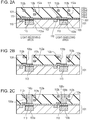
- FIG. 1 is a cross-sectional view of a schematic structure of the solid-state image pickup device, indicated at 100, according to this example.
- a single pixel is illustrated in the light-receiving area and a single pixel is illustrated in the light-shielding area.
- a plurality of pixels are arranged in matrix in the light-receiving area.
- a plurality of pixels are arranged in the light-shielding area.
- electrons are signal carriers. Holes may be signal carriers. In the case where holes serve as signal carriers, the conduction types of semiconductor regions may be reversed.
- a semiconductor substrate 101 is an n-type epitaxial layer. In the semiconductor substrate 101, p-type semiconductor regions and n-type semiconductor regions are arranged.
- the semiconductor substrate 101 has a principal surface 102.
- the principal surface 102 is the interface between the semiconductor substrate 101 and a thermally-oxidized film (not illustrated) laminated on the semiconductor substrate 101. Light passes through the principal surface 102 and enters the semiconductor substrate 101.
- the arrows L denote the direction of incidence of light.
- Photoelectric conversion units 103a and 103b are photodiodes, for example.
- the photoelectric conversion units 103a and 103b each include an n-type semiconductor region constituting the photodiode. Carriers caused by photoelectric conversion are collected in the n-type semiconductor region.
- Each p-type semiconductor region 109 is disposed in contact with the principal surface 102 of the semiconductor substrate 101.
- the area of the photoelectric conversion unit 103a may be different from that of the photoelectric conversion unit 103b.
- the photoelectric conversion unit 103b may include no n-type semiconductor region.
- the photoelectric conversion unit 103b is shielded from light, such that a signal from the photoelectric conversion unit 103b may be used as a black level reference signal.
- the photoelectric conversion unit 103b may include no n-type semiconductor region. In addition, so long as electrons in the photoelectric conversion unit 103b can be read as signals, photoelectric conversion is not necessarily needed in the photoelectric conversion unit 103b.
- Each floating diffusion (FD) region 110 is an n-type semiconductor region. Carries generated in each photoelectric conversion unit 103 is transferred to the corresponding FD region 110 and is converted into a voltage.
- the FD region 110 is electrically connected to an input node of an amplifying unit (not illustrated). Alternatively, the FD region 110 may be electrically connected to a signal output line (not illustrated).
- Each gate electrode 111 is disposed above the semiconductor substrate 101, with the thermally-oxidized film (not illustrated) therebetween. The gate electrodes 111 control carrier transfer between the photoelectric conversion unit 103a and the corresponding FD region 110 and that between the photoelectric conversion unit 103b and the corresponding FD region 110, respectively.
- An insulator 104 is disposed adjacent to the principal surface 102 of the semiconductor substrate 101.
- the insulator 104 is a silicon oxide film.
- a refractive index of the insulator 104 may be in the range of 1.40 to 1.60.
- a first interconnect layer 112a and a second interconnect layer 112b are arranged adjacent to the principal surface 102 of the semiconductor substrate 101.
- the first and second interconnect layers 112a and 112b are arranged at different levels relative to the principal surface 102 of the semiconductor substrate 101.
- the conductive members of the first and second interconnect layers 112a and 112b comprise copper.
- the conductive members may comprise a conductive material other than copper.
- Part of the conductive member of the first interconnect layer 112a and part of the conductive member of the second interconnect layer 112b may be electrically connected to each other through a plug (not illustrated).
- the conductive members, excluding the parts electrically connected through the plug, of the first and second interconnect layers 112a and 112b are isolated from each other by the insulator 104.
- the insulator 104 may include an insulating interlayer.
- the number of interconnect layers is not limited to two. A single interconnect layer or three or more interconnect layers may be arranged.
- the pixel in the light-receiving area and the pixel in the light-shielding area have the same pattern of the conductive member included in the first interconnect layer 112a or the second interconnect layer 112b.
- the pixels in these areas have the same pattern of the conductive member included in at least the first interconnect layer 112a.
- the same pattern may be a conductive pattern of at least a portion constituting an electrical node up to the signal output line disposed on the rear of each pixel.
- a hole 105a and a hole 105b are arranged in the insulator 104.
- the hole 105a is associated with the photoelectric conversion unit 103a.
- the hole 105b is associated with the photoelectric conversion unit 103b.
- a waveguide member 106a is disposed in the hole 105a.
- a waveguide member 106b is disposed in the hole 105b.
- each of the waveguide members 106a and 106b is a silicon nitride film.
- each of the waveguide members 106a and 106b may be a silicon oxynitride film or comprise an organic material (resin, such as polyimide polymer).
- a refractive index of the waveguide members 106a and 106b is higher than that of the insulator 104.
- the refractive index of the waveguide members 106a and 106b may be greater than or equal to 1.60.
- the refractive index thereof may be in the range of 1.80 to 2.40.
- the hole 105a is filled with the waveguide member 106a.
- the waveguide member 106a may, however, be disposed in only part of the hole 105a.
- the waveguide member 106a may comprise a plurality of materials. In this case, the refractive index of any one of the materials may be higher than that of the insulator 104.
- the waveguide member 106a may include a silicon nitride film and a silicon oxynitride film.
- a silicon nitride film may be disposed on the side wall of the hole 105a and in the vicinity of the bottom thereof and an organic material may be disposed in the other portion of the hole 105a.
- the description about the hole 105a and the waveguide member 106a can be applied to the hole 105b and the waveguide member 106b unless otherwise noted.
- An etching stopper 113 is disposed between the semiconductor substrate 101 and each of the waveguide members 106a and 106b.
- the etching stopper 113 is a layer to accurately stop etching in the formation of the holes 105a and 105b.
- the etching stopper 113 may be a layer to delay etching.
- the etching stoppers 113 are in contact with the waveguide members 106a and 106b, respectively.
- the etching stoppers 113 serve as the bottoms of the holes 105a and 105b adjacent to the semiconductor substrate 101.
- Each etching stopper 113 comprises a material different from that of the insulator 104.
- the etching stopper 113 is a silicon nitride film.
- the etching stopper 113 may be omitted depending on etching conditions.
- the etching stoppers 113 may be removed in etching for forming the holes 105a and 105b.
- a light-shielding member 108 comprises metal or an organic material that is not transmissive to light.
- the material of the light-shielding member 108 may exhibit a high reflectivity to light having a wavelength of 400 to 600 nm.
- the light-shielding member 108 comprises aluminum.
- the light-shielding member 108 is disposed over the photoelectric conversion unit 103b.
- the light-shielding member 108 may be disposed over the light-shielding area.
- the light-shielding member 108 does not have to block the whole of light entering the photoelectric conversion unit 103b. For example, light obliquely traveling from a portion where the light-shielding member 108 is not disposed may enter the photoelectric conversion unit 103b after multiple reflections.
- the light-shielding member 108 may be part of a conductive member included in a third interconnect layer.
- the light-shielding member 108 may serve as an interconnect for transmitting a power supply voltage or a signal.
- the third interconnect layer including the light-shielding member 108 may include a conductive member which serves as pads or interconnects for peripheral circuits.
- the third interconnect layer where the light-shielding member 108 is disposed may include only the light-shielding member 108.
- d1 denotes the distance (first distance) between the principal surface 102 of the semiconductor substrate 101 and an opposite surface 107a of the waveguide member 106a from the semiconductor substrate 101.
- d2 denotes the distance (second distance) between the principal surface 102 of the semiconductor substrate 101 and an opposite surface 107b of the waveguide member 106b from the semiconductor substrate 101.
- d3 denotes the distance (third distance) between the principal surface 102 of the semiconductor substrate 101 and the light-shielding member 108.
- d4 denotes the distance (fourth distance) between the principal surface 102 of the semiconductor substrate 101 and an opposite surface of the conductive member, included in the first interconnect layer 112a, from the semiconductor substrate 101.
- the distance 3 between the principal surface 102 and the light-shielding member 108 is greater than the distance d1 between the principal surface 102 and the opposite surface 107a of the waveguide member 106a from the semiconductor substrate 101 and the distance d2 between the principal surface 102 and the opposite surface 107b of the waveguide member 106b from the semiconductor substrate 101.
- the light-shielding member 108 is disposed farther from the semiconductor substrate 101 than the waveguide members 106a and 106b.
- the distance d1 between the principal surface 102 and the opposite surface 107a of the waveguide member 106a from the semiconductor substrate 101 and the distance d2 between the principal surface 102 and the opposite surface 107b of the waveguide member 106b from the semiconductor substrate 101 are greater than the distance d4.
- at least part of each of the waveguide members 106a and 106b is disposed farther from the semiconductor substrate 101 than the first interconnect layer 112a which is the closest to the semiconductor substrate 101.
- the distance d1 between the principal surface 102 and the opposite surface 107a of the waveguide member 106a from the semiconductor substrate 101 and the distance d2 between the principal surface 102 and the opposite surface 107b of the waveguide member 106b from the semiconductor substrate 101 are greater than the distance between the principal surface 102 and the opposite surface of the conductive member, included in the second interconnect layer 112b, from the semiconductor substrate 101.
- the distance d1 and the distance d2 are to be greater than at least the distance d4 between the principal surface 102 and the opposite surface of the conductive member, included in the interconnect layer closest to the semiconductor substrate 101, from the semiconductor substrate 101.
- the distance between the principal surface 102 and the surface of the waveguide member 106a facing the semiconductor substrate 101 and the distance between the principal surface 102 and the surface of the waveguide member 106b facing the semiconductor substrate 101 are less than the distance between the principal surface 102 and the surface of the conductive member, included in the first interconnect layer 112a, facing the semiconductor substrate 101.
- the arrangement is not limited to the above-described one.
- the distance between the principal surface 102 and the surface of the waveguide member 106a facing the semiconductor substrate 101 and the distance between the principal surface 102 and the surface of the waveguide member 106b facing the semiconductor substrate 101 may be less than the distance between the principal surface 102 and the surface of the conductive member, included in the second interconnect layer 112b, facing the semiconductor substrate 101 and may be greater than the distance d4 between the principal surface 102 and the opposite surface of the conductive member, included in the first interconnect layer 112a, from the semiconductor substrate 101.
- the surface of the waveguide member 106a facing the semiconductor substrate 101 is disposed apart from the principal surface 102 by a predetermined distance.
- the waveguide members 106a and 106b may, however, be in contact with the semiconductor substrate 101.
- An intralayer lens 114 converges light traveling toward the semiconductor substrate 101 on the photoelectric conversion unit 103a or the waveguide member 106a.
- the intralayer lens 114 is disposed on an opposite side of the waveguide member 106a from the semiconductor substrate 101.
- the intralayer lens 114 is disposed in association with the photoelectric conversion unit 103a in the light-receiving area.
- the intralayer lens 114 comprises a silicon nitride film.
- the placement of the intralayer lens 114 is not necessarily needed.
- a color filter and a top lens may be arranged on an opposite side of the intralayer lens 114 from the semiconductor substrate 101.
- FIG. 2A to 3C components having the same functions as those in Fig. 1 are designated by the same reference numerals and detailed description thereof is omitted.
- Fig. 2A illustrates a step of forming the semiconductor regions in the semiconductor substrate 101 and forming a gate electrode 111, the insulator 104, the etching stoppers 113, and the first and second interconnect layers 112a and 112b above the semiconductor layer 101.
- the photoelectric conversion units 103a and 103b and the FD regions 110 are formed in the semiconductor substrate 101 such that the portions and the regions are arranged in the vicinity of the principal surface 102.
- source and drain regions of other transistors in pixel portions may be formed.
- the gate electrodes 111 are then formed.
- gate electrodes of the other transistors in the pixel portions may be formed.
- a protective layer 201 is formed on the principal surface 102 adjacent to which the photoelectric conversion units 103a and 103b are arranged.
- the protective layer 201 is a silicon nitride film.
- the protective layer 201 may be composed of a plurality of layers including a silicon nitride film and a silicon oxide film.
- the protective layer 201 may have a function of reducing damage to be applied to the photoelectric conversion units in a subsequent step.
- the protective layer 201 may have an antireflection function.
- the etching stoppers 113 are formed on an opposite surface of the protective layer 201 from the semiconductor substrate 101.
- the areas of the etching stoppers 113 may be greater than the areas of the respective bottoms of the holes 105a and 105b to be formed later. Furthermore, the etching stoppers 113 may be omitted in an area other than the bottoms of the holes 105a and 105b. Note that formation of the protective layer 201 and the etching stoppers 113 is not necessarily needed.
- the insulator 104, the first interconnect layer 112a, and the second interconnect layer 112b are then formed.
- the first and second interconnect layers 112a and 112b are formed using a damascene process.
- a case where the insulator 104 is composed of a plurality of insulating interlayers 104a to 104e will be described.
- the insulating interlayers will be called first to fifth insulating interlayers 104a to 104e in order from the interlayer closest to the semiconductor substrate 101.
- the first insulating interlayer 104a is formed so as to fully cover the light-receiving area and the light-shielding area. An opposite surface of the first insulating interlayer 104a from the semiconductor substrate 101 may be planarized as necessary. Through-holes (not illustrated) are formed in the first insulating interlayer 104a. In the through-holes, plugs electrically connecting the conductive member in the first interconnect layer 112a to the semiconductor regions in the semiconductor substrate 101 are arranged.
- the second insulating interlayer 104b is formed on an opposite side of the first insulating interlayer 104a from the semiconductor substrate 101.
- portions corresponding to regions where the conductive member in the first interconnect layer 112a is to be disposed are removed by etching.
- a metal film, serving as the first interconnect layer 112a is formed so as to fully cover the light-receiving area and the light-shielding area.
- the metal film is removed by a method, such as CMP, such that the second insulating interlayer 104b is exposed.
- the conductive member which serves as the interconnects in the first interconnect layer 112a is disposed in a predetermined pattern in the above-described manner.
- the third insulating interlayer 104c and the fourth insulating interlayer 104d are formed so as to fully cover the light-receiving area and the light-shielding area.
- portions corresponding to regions where the conductive member in the second interconnect layer 112b is to be disposed are removed by etching.
- portions corresponding to regions where plugs electrically connecting the conductive member in the first interconnect layer 112a to the conductive member in the second interconnect layer 112b are to be arranged are removed by etching.
- a metal film serving as the second interconnect layer 112b and the plugs, is formed so as to fully cover the light-receiving area and the light-shielding area. Then, the metal film is removed by a method, such as CMP, such that the fourth insulating interlayer 104d is exposed. An interconnect pattern in the second interconnect layer 112b and a plug pattern are obtained in the above-described manner. After formation of the third and fourth insulating interlayers 104c and 104d, the portions corresponding to the regions where the plugs electrically connecting the conductive member in the first interconnect layer 112a to that in the second interconnect layer 112b are to be arranged may be removed by etching.
- the fifth insulating interlayer 104e is formed so as to fully cover the light-receiving area and the light-shielding area.
- An opposite surface of the fifth insulating interlayer 104e from the semiconductor substrate 101 may be planarized as necessary.
- an etching stopping film, an antireflection metal film, or a film having functions of both of those films may be disposed between the adjacent insulating interlayers.
- the insulator 104 is a silicon oxide film
- a silicon nitride film serves as an antireflection metal film.
- the first and second interconnect layers 112a and 112b may be formed by a method other than a damascene process. A method other than a damascene process will now be described.
- the metal film serving as the first interconnect layer 112a, is formed so as to fully cover the light-receiving area and the light-shielding area.
- portions other than the regions where the conductive member in the first interconnect layer 112a is disposed are removed by etching.
- the interconnect pattern of the first interconnect layer 112a is obtained.
- the second insulating interlayer 104b and the third insulating interlayer 104c are formed and the second interconnect layer 112b is similarly formed.
- the fourth insulating interlayer 104d and the fifth insulating interlayer 104e are formed. Opposite surfaces of the third and fifth insulating interlayers 104c and 104e from the semiconductor substrate 101 are planarized as necessary.
- the insulator 104 may be formed in a region associated with the photoelectric conversion unit 103a and a region associated with the photoelectric conversion unit 103b at the same time. The reason is that the insulator 104 serves as the side walls of the holes 105a and 105b. The difference in noise between the photoelectric conversion units 103a and 103b caused by different steps of forming the insulator 104 is, however, small. Accordingly, the insulator 104 may be formed in the region associated with the photoelectric conversion unit 103a and the region associated with the photoelectric conversion unit 103b by different steps.
- An interconnect structure of the first and second interconnect layers 112a and 112b in the light-receiving area may coincide with that in the light-shielding area.
- the parasitic capacitance between the interconnects in the light-receiving area can be substantially equal to that in the light-shielding area.
- Fig. 2B illustrates forming the holes 105a and 105b in the insulator 104.
- An etching mask pattern (not illustrated) is disposed on an opposite side of the insulator 104 from the semiconductor substrate 101.
- the etching mask pattern covers a region other than the regions where the holes 105a and 105b are to be arranged.
- the etching mask pattern has an opening corresponding to the region where the hole 105a is to be disposed and another opening corresponding to the region where the hole 105b is to be disposed.
- the etching mask pattern is a photoresist patterned by, for example, photolithography and development.
- the insulator 104 is then etched using the etching mask pattern as a mask. Thus, the holes 105a and 105b are simultaneously formed. After etching of the insulator 104, the etching mask pattern is removed.
- etching can be performed in Fig. 2B such that the etching stoppers 113 are exposed.
- the etching stoppers 113 may have an etching rate lower than that of the insulator 104 under etching conditions for etching the insulator 104.
- the etching stoppers 113 may comprise a silicon nitride film or a silicon oxynitride film.
- the etching stoppers 113 may be exposed by a plurality of etching processes under different conditions.
- a feature of one aspect of this embodiment is that the insulator 104 positioned in the region where the hole 105a is to be formed and the insulator 104 positioned in the region where the hole 105b is to be formed are simultaneously etched. Accordingly, the etching mask pattern used for etching has an opening corresponding to the region where the hole 105a is to be disposed and another opening corresponding to the region where the hole 105b is to be disposed. Etching the insulator 104 using such an etching mask pattern allows the holes 105a and 105b to be simultaneously formed. In the above-described step, the holes 105a and 105b having substantially the same shape can be formed, except for an influence of, for example, unevenness in the plane of the semiconductor substrate 101. Furthermore, damage caused by etching to the photoelectric conversion unit 103a may substantially coincide with that to the photoelectric conversion unit 103b.
- Fig. 2C illustrates forming the waveguide members 106a and 106b in the holes 105a and 105b, respectively.
- the material of the waveguide members 106a and 106b is deposited so as to fully cover the light-receiving area and the light-shielding area.
- the deposition of the material of the waveguide members 106a and 106b can be achieved by film formation by chemical vapor deposition (CVD) or sputtering, or application of an organic material, such as polyimide polymer. After that, the material of the waveguide members 106a and 106b protruding from the holes 105a and 105b is removed as necessary.
- CVD chemical vapor deposition
- sputtering or application of an organic material, such as polyimide polymer.
- Each of the waveguide members 106a and 106b may be formed such that the opposite end of the waveguide member from the semiconductor substrate 101 is farther from the principal surface 102 of the semiconductor substrate 101 than the second interconnect layer 112b.
- the waveguide members 106a and 106b are arranged in contact with the respective etching stoppers 113.
- the waveguide members 106a and 106b may be formed by multiple depositions of the same material. Furthermore, the waveguide members 106a and 106b can be formed by sequential depositions of different materials. For example, a silicon nitride film may be formed and an organic material having high filling ability may then be formed, thus forming the waveguide members 106a and 106b.
- any material having a higher refractive index than that of the insulator 104 may be used.
- the insulator 104 is a silicon oxide film
- examples of the material of the waveguide members 106a and 106b include a silicon nitride film and a polyimide organic material.
- the refractive index of the silicon nitride film is approximately 2.0.
- the refractive index of the surrounding silicon oxide film is approximately 1.4. Accordingly, light incident on the interface between the insulator 104 and each of the waveguide members 106a and 106b is reflected according to Snell's law. Consequently, the light can be trapped in the waveguide members 106a and 106b.
- the content of hydrogen in the silicon nitride film can be increased, so that dangling bonds from the substrate can be terminated due to the effect of hydrogen supply. Consequently, noise, such as a white defect, can be reduced.
- the refractive index of the polyimide organic material is approximately 1.7.
- the filling ability of the polyimide organic material is higher than that of the silicon nitride film.
- the material of the waveguide members 106a and 106b may be appropriately chosen in consideration of the balance between optical characteristics, such as the difference between refractive indices, and benefits of making steps.
- a feature of this embodiment is that the waveguide members 106a and 106b are simultaneously formed.
- the material of the waveguide members 106a and 106b is deposited in one of the holes 105a and 105b, the material is deposited in the other hole.
- the waveguide members 106a and 106b having substantially the same shape can be formed, except for an influence of, for example, unevenness in the plane of the semiconductor substrate 101.
- Fig. 3A illustrates forming a first planarization film 301 and the light-shielding member 108.
- the first planarization film 301 is formed on the opposite side of the waveguide members 106a and 106b from the semiconductor substrate 101.
- the first planarization film 301 is a silicon oxide film.
- An opposite surface of the first planarization film 301 from the semiconductor substrate 101 is then planarized by CMP.
- the method of planarization is not limited to CMP. A known method, such as etching or polishing, can be used. In the case where the surface, where the first planarization film 301 is to be formed, is planarized before formation of the film 301, planarization after formation of the film 301 is not necessarily needed.
- the light-shielding member 108 is formed on an opposite side of the first planarization film 301 from the semiconductor substrate 101.
- the light-shielding member 108 is disposed in association with the photoelectric conversion unit 103b in the light-shielding area.
- the light-shielding member 108 reflects or absorbs light traveling toward the photoelectric conversion unit 103b. Accordingly, light-reflective metal or a light-absorbing organic material is suitable for the material of the light-shielding member 108.
- the light-shielding member 108 comprises aluminum.
- the method of making the first interconnect layer 112a or the second interconnect layer 112b may be appropriately used.
- the light-shielding member 108 may be included in the third interconnect layer. Specifically, in the step of forming the light-shielding member 108, the conductive member which serves as pads or interconnects for the peripheral circuits can be simultaneously formed. The light-shielding member 108 may serve as an interconnect.
- Fig. 3B illustrates forming the intralayer lens 114.
- the intralayer lens 114 is formed on the opposite side of the first planarization film 301 from the semiconductor substrate 101.
- the intralayer lens 114 is disposed in association with the photoelectric conversion unit 103a in the light-receiving area.
- the intralayer lens 114 comprises, for example, a silicon nitride film.
- a method of making the intralayer lens 114 a known method can be used.
- the surface of the light-shielding member 108 facing the semiconductor substrate 101 is in contact with the first planarization film 301.
- the surface of the intralayer lens 114 facing the semiconductor substrate 101 is in contact with the first planarization film 301.
- the light-shielding member 108 and the intralayer lens 114 are arranged in contact with the same film (e.g., the first planarization film 301), the opposite surface of the film from the semiconductor substrate 101 being planarized.
- the difference in level between the light-receiving area and the light-shielding area can be reduced.
- a refractive index of the first planarization film 301 is lower than that of the intralayer lens 114.
- the refractive index of the silicon nitride film which serves as the intralayer lens 114 is approximately 2.0 and that of the silicon oxide film which serves as the first planarization film 301 is approximately 1.46.
- sensitivity to oblique incident light can be increased. The reason is as follows. Oblique incident light (indicated at an arrow L1) is not fully converged by the intralayer lens 114, so that the light does not enter the waveguide member 106a in some cases.
- a dotted line indicates the optical path of the light in this case.
- the oblique incident light is converged by the intralayer lens 114 and is then refracted to an optical axis OP.
- a broken line indicates the optical axis OP. Since the oblique incident light enters the waveguide member 106a as described above, sensitivity to the oblique incident light can be increased.
- Fig. 3C illustrates forming a color filter 303 and a microlens 304.
- a second planarization film 302 is formed so as to cover the light-shielding member 108 and the intralayer lens 114.
- the second planarization film 302 is an insulator.
- the second planarization film 302 is, for example, a silicon oxide film.
- An opposite surface of the second planarization film 302 from the semiconductor substrate 101 is planarized as necessary.
- the color filter 303 and the microlens 304 are formed in a region associated with the photoelectric conversion unit 103a in the light-receiving area.
- the color filter 303 and the microlens 304 are arranged as necessary.
- any one of a portion associated with the first photoelectric conversion unit 103a and another portion associated with the second photoelectric conversion unit 103b is not removed.
- the insulator 104 is etched in both the light-receiving area and the light-shielding area simultaneously. As long as etching the insulator 104 is performed in both the light-receiving area and the light-shielding area simultaneously, the holes 105a and 105b can be formed at the same time.
- the step of etching the insulator 104 using the etching mask having the opening corresponding to the region where the hole 105a is to be formed and the other opening corresponding to the region where the hole 105b is to be formed is a step of simultaneously forming the holes 105a and 105b.
- the etching mask has only the opening corresponding to the region where the hole 105a is to be formed, only the portion of the insulator 104 corresponding to the hole 105a will be etched in the subsequent etching step (not claimed). In this step, the holes 105a and 105b are not simultaneously formed.
- the material of the waveguide members 106a and 106b is deposited in both the holes 105a and 105b simultaneously. As long as the material of the waveguide members 106a and 106b is deposited both in the holes 105a and 105b simultaneously, the waveguide members 106a and 106b can be formed at the same time. All of the steps from the step of forming the semiconductor regions in the semiconductor substrate 101 to the step of forming the waveguide members 106a and 106b are simultaneously performed in both the light-receiving area and the light-shielding area.
- the waveguide members 106a and 106b are not simultaneously formed.
- the second planarization film 302 is formed. In the second planarization film 302, only one of a portion associated with the first photoelectric conversion unit 103a and another portion associated with the second photoelectric conversion unit 103b is not removed.
- Figs. 4A to 4C components having the same functions as those in Figs. 1 to 3C are designated by the same reference numerals and detailed description thereof is omitted.
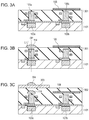
- Fig. 4A is a plan view of a schematic structure of the solid-state image pickup device 100 according to this embodiment.
- a light-receiving area 401, a light-shielding area 402, and a peripheral circuit area 403 are illustrated.
- a plurality of pixels each including the photoelectric conversion unit are arranged in the light-receiving area 401 and the light-shielding area 402.
- an array of 1920 x 1080 pixels can be disposed in the light-receiving area 401.
- the photoelectric conversion units arranged in the light-shielding area 402 are shielded from light.
- the light-shielding area 402 is positioned between the light-receiving area 401 and the peripheral circuit area 403.
- peripheral circuit area 403 circuits used for operations of the solid-state image pickup device 100 are arranged.
- signal processing circuits for processing signals from the photoelectric conversion units are arranged in the peripheral circuit area 403.
- the circuits arranged in the peripheral circuit area 403 include, for example, a vertical shift register, a horizontal shift register, an amplifier, an analog-to-digital converter (ADC), and a memory.
- the amplifier, the ADC, and the memory may be arranged for each row of the photoelectric conversion units arranged in the array.
- Figs. 4B and 4C are cross-sectional views of schematic structures of the solid-state image pickup device 100 taken along the lines AB, CD, and EF in Fig. 4A.
- Fig. 4B illustrates the cross sections, where the etching stoppers 113 are arranged, in the step of Fig. 2B .
- Fig. 4C illustrates the cross sections, where the etching stoppers 113 are not arranged, in the step of Fig. 2B .
- the cross section taken along the line AB includes a pixel 401a disposed in the light-receiving area 401.
- the cross section taken along the line CD includes a pixel 410b disposed in the light-receiving area 401 and a pixel disposed in the light-shielding area 402.
- the pixel 401b is positioned farther from the center of the light-receiving area 401 than the pixel 401a.
- the pixel 401b is positioned next to the pixel disposed in the light-shielding area 402.
- the cross section taken along the line EF corresponds to the peripheral circuit area 403.
- the step of forming the first interconnect layer 112a and the second interconnect layer 112b includes planarizing.
- the difference in level between the insulator 104 in the light-receiving area 401 and that in the peripheral circuit area 403 may occur. This is caused by, for example, the difference in a density of arranged plugs between the light-receiving area 401 and the peripheral circuit area 403.
- the density of plugs means the number of plugs per unit area in plane.
- the light-receiving area 401 in which the density of plugs is high may be recessed relative to the peripheral circuit area 403 by planarization.
- the difference in level may be caused due to, for example, the difference in the density of interconnects between these areas. Accordingly, the difference in level between the insulator 104 in the light-receiving area 401 and that in the light-shielding area 402 near the peripheral circuit area 403 may also be caused.
- h1 denotes the distance between the principal surface 102 of the semiconductor substrate 101 and an opposite surface of the insulator 104 from the semiconductor substrate 101 in the pixel 401a and h2 denotes the distance between the principal surface 102 of the semiconductor substrate 101 and the opposite surface of the insulator 104 from the semiconductor substrate 101 in the light-shielding area 402.
- the distance h1 differs from the distance h2 as illustrated in Figs. 4B and 4C . The difference in level does not tend to occur in a pixel positioned in close proximity to a pixel in the light-shielding area 402.
- the height of the solid-state image pickup device 100 gradually varies from the peripheral circuit area 403 to the center of the light-receiving area 401. Accordingly, the distance, indicated at h3, between the principal surface 102 of the semiconductor substrate 101 and the opposite surface of the insulator 104 from the semiconductor substrate 101 in, for example, the pixel 401b next to the pixel included in the light-shielding area 402 is approximately equal to the distance h2.
- the insulator 104 may be etched in the step of Fig. 2B such that the etching stoppers 113 are exposed. Since the etching rate of the etching stoppers 113 is low, etching hardly proceeds after exposure of the etching stoppers 113. Since the etching stoppers 113 serve as the respective bottoms of the holes 105a and 105b, the distance between the principal surface 102 of the semiconductor substrate 101 and the bottom of the hole 105a in the pixel 401a is substantially equal to the distance between the principal surface 102 of the semiconductor substrate 101 and the bottom of the hole 105b in the light-shielding area 402. In Figs.
- z1 denotes the distance between the principal surface 102 of the semiconductor substrate 101 and the bottom of the hole 105a in the light-receiving area 401 and z2 denotes the distance between the principal surface 102 of the semiconductor substrate 101 and the bottom of the hole 105b in the light-shielding area 402.
- the distance z1 is approximately equal to the distance z2.
- the insulator 104 is etched by an amount depending on etching time. Accordingly, the distance z1 differs from the distance z2 as illustrated in Fig. 4C . The reason is that the above-described difference reflects the original unevenness of the insulator 104.
- the arrangement of the etching stoppers 113 allows the distance z1 (the level of the bottom of the hole 105a) in the light-receiving area 401 and the distance z2 (the level of the bottom of the hole 105b) in the light-shielding area 402 to be approximately equal to each other. Consequently, the difference between noise caused in the photoelectric conversion unit in the light-receiving area 401 and that in the light-shielding area 402 can be reduced, so that image quality can be increased.
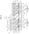
- FIG. 5A is a cross-sectional view of a schematic structure of a solid-state image pickup device 100 according to a second example.
- Fig. 5B is a plan view of the schematic structure of the solid-state image pickup device 100 according to the second example.
- Components having the same functions as those in Figs. 1 to 4C are designated by the same reference numerals and detailed description is omitted.
- a feature of this example is that light-shielding members 501a to 501c are arranged such that each member is disposed between the adjacent photoelectric conversion units arranged in the light-receiving area.
- the second example may provide the same structure as that in the first embodiment, except for this arrangement.
- a photoelectric conversion unit 103a and a photoelectric conversion unit 103c are arranged in the light-receiving area.
- a waveguide member 106a is disposed in association with the photoelectric conversion unit 103a.
- a waveguide member 106c is disposed in association with the photoelectric conversion unit 103c.
- the photoelectric conversion unit 103c and the waveguide member 106c are designated by the reference numerals different from those of the photoelectric conversion unit 103a and the waveguide member 106a.
- the photoelectric conversion units 103a and 103c however, have the same function.
- the waveguide members 106a and 106c have the same function. Accordingly, the description of the photoelectric conversion unit 103a and that of the waveguide member 106a in the first embodiment can be appropriately applied to the photoelectric conversion unit 103c and the waveguide member 106c.
- the light-shielding member 501b is disposed between the waveguide member 106a disposed in association with the photoelectric conversion unit 103a and the waveguide member 106c disposed in association with the photoelectric conversion unit 103c.
- the reason why the light-shielding member 501b is disposed between the waveguide members 106a and 106c is as follows. When the waveguide members 106a and 106b and the light-shielding member 501b are projected on the same plane, the light-shielding member 501b is projected between a region where the waveguide member 106a is projected and a region where the waveguide member 106c is projected.
- the light-shielding member 501a is disposed between the waveguide member 106a and a waveguide member associated with a photoelectric conversion unit of another pixel next to the photoelectric conversion unit 103a.
- the light-shielding member 501c is disposed between the waveguide member 106c and a waveguide member associated with a photoelectric conversion unit of another pixel next to the photoelectric conversion unit 103c.
- the same material as that of the light-shielding member 108 can be appropriately used.
- the material of the light-shielding members 501a to 501c may be the same as that of the light-shielding member 108.
- the light-shielding members 501a to 501c comprise aluminum.
- the light-shielding members 501a to 501c are arranged farther from the semiconductor substrate 101 than the waveguide members 106a and 106c.
- the light-shielding members 501a to 501c may be arranged in the same interconnect layer as that including the light-shielding member 108.
- the light-shielding members 501a to 501c can be formed without increase of the number of interconnect forming steps.
- the light-shielding member 108 and the light-shielding members 501a to 501c are arranged in a third interconnect layer.
- Fig. 5B is a plan view of the schematic structure of the solid-state image pickup device 100 according to this example.
- the cross section taken along the line VA-VA in Fig. 5B is illustrated in Fig. 5A .
- the light-shielding member 501b is disposed between the waveguide member 106a associated with the photoelectric conversion unit 103a and the waveguide member 106c associated with the photoelectric conversion unit 103c.
- the photoelectric conversion unit 103a may be surrounded by the light-shielding members 501a and 501b and light-shielding members 501d.
- the light-shielding members may be arranged in a lattice pattern in the light-receiving area and each photoelectric conversion unit may be disposed in a region surrounded by the light-shielding members.
- the arrangement is not limited to this one.
- the light-shielding member 501b may be disposed in only the region between the photoelectric conversion units 103a and 103c.
- the light-shielding member 108 may be disposed so as to fully cover the light-shielding area. Thus, the quantity of light entering photoelectric conversion units 103b arranged in the light-shielding area can be reduced.
- the solid-state image pickup device 100 may further include an intralayer lens 114, a color filter 303, and a microlens 304.
- the method includes the same steps as those illustrated in Figs. 2A to 2C in the first embodiment.
- the step illustrated in Fig. 3A when the light-shielding member 108 is formed, the light-shielding members 501a to 501c included in the same interconnect layer are formed.
- the light-shielding member 501b is disposed between the waveguide members 106a and 106c in the light-receiving area.
- the quantity of light entering a region excluding the waveguide members 106a and 106c can be reduced.
- light entering a region excluding the waveguide members 106a and 106c light is likely to enter a region excluding the photoelectric conversion units in the semiconductor substrate 101. Accordingly, the light entering the region excluding the waveguide members 106a and 106c causes noise, such as color mixture.
- This example therefore, has a benefit in that noise can be further reduced in addition to the benefits of the first embodiment.
- FIG. 6 is a cross-sectional view of a schematic structure of the solid-state image pickup device, indicated at 100.
- Components having the same functions as those in Figs. 1 to 5B are designated by the same reference numerals and detailed description thereof is omitted.
- a feature of this example is the structure of an intralayer lens 601 disposed on an opposite side of a waveguide member 106a from a semiconductor substrate 101.
- the intralayer lens 114 in the first embodiment is a convex lens that protrudes far away from the semiconductor substrate 101.
- such a lens will be referred to as an "upwardly protruding lens”.
- the intralayer lens 601 is a convex lens that protrudes toward the semiconductor substrate 101.
- such a lens will be referred to as a "downwardly protruding lens”.
- a method of forming the intralayer lens 601, serving as a downwardly protruding lens, will now be described.
- the method includes the same steps as those illustrated in Figs. 2A to 2C in the first embodiment.
- a light-shielding member 108 when a light-shielding member 108 is formed, light-shielding members 501a to 501c included in the same interconnect layer are formed. At this time, the light-shielding members 501a and 501c are arranged in a grid pattern.
- a base member 602 is formed. The base member 602 is disposed so as to cover the light-shielding members 501a to 501c.
- irregularities are caused on the base member 602 by the difference in level between regions where the light-shielding members 501a to 501c are arranged and regions where the light-shielding members 501a to 501c are not arranged. Since the light-shielding members 501a to 501c are arranged in a grid pattern so as to surround each photoelectric conversion unit, a depression is disposed in each region, associated with the photoelectric conversion unit, in the base member 602. A material having a higher refractive index than that of the base member 602 is then deposited on an opposite side of the base member 602 from the semiconductor substrate 101.
- the intralayer lens 601, serving as a downwardly protruding lens, can be formed by the above-described steps.
- an opposite surface of the intralayer lens 601 from the semiconductor substrate 101 may be planarized as necessary.
- a color filter 303 and microlenses 304 may be further formed.
Description
- The present invention relates to a solid-state image pickup device and a method of making the same.
- Prior art which is related to this field of technology can be found in e.g. document
WO 2010/113634 A1 disclosing an image sensor and a manufacturing method thereof, in documentUS 2009/0166783 A1 disclosing a solid-state imaging device, a method of manufacturing the same, and a camera and an electronic apparatus using the same, in documentUS 2009/0286346 A1 disclosing methods for forming anti-reflection structures for CMOS image sensors, in documentUS 2004/0238908 A1 disclosing a photoelectric conversion device and a manufacturing method thereof, in documentUS2006/0115230A1 disclosing solid-state imaging device and production method therefor, in documentUS 2009/0251573A1 disclosing solid-state imaging apparatus and manufacturing method thereof, and in documentJP2007-141873A - Solid-state image pickup devices have recently been proposed which include an optical waveguide in order to increase the quantity of light incident on a photoelectric conversion unit.
- Japanese Patent Laid-Open No.
2007-141873 Fig. 1 disclosed in Japanese Patent Laid-Open No.2007-141873 - The solid-state image pickup device disclosed in Japanese Patent Laid-Open No.
2007-141873 Fig. 1 of Japanese Patent Laid-Open No.2007-141873 - Second, the parasitic capacitance of an interconnect for signal transmission of each pixel in the light-receiving area may differ from that of each pixel in the light-shielding area. The reason is that the structures of interconnects in the light-receiving area markedly differ from those in the light-shielding area. Specifically, the structure of a first interconnect closest to the semiconductor substrate in the light-receiving area differs from that in the light-shielding area.
- Third, the extent of damage caused by a making process in the light-receiving area may differ from that in the light-shielding area. The reason is that a process of forming the optical waveguide of each pixel in the light-receiving area differs from that in the light-shielding area.
- The above-described first to third disadvantages may increase the difference in noise between pixels in the light-receiving area and pixels in the light-shielding area.
- The present invention provides a solid-state image pickup device as specified in the appended device claims.
- The present invention provides a method of making a solid-state image pickup device as specified in the appended method claims.
- Further features of the present invention will become apparent from the following description of exemplary embodiments with reference to the attached drawings.
-
Fig. 1 is a cross-sectional view of a schematic structure of a solid-state image pickup device according to a first example useful for understanding the invention. -
Fig. 2A is a diagram illustrating a method of making the solid-state image pickup device according to the first embodiment. -
Fig. 2B is a diagram illustrating the method of making the solid-state image pickup device according to the first embodiment. -
Fig. 2C is a diagram illustrating the method of making the solid-state image pickup device according to the first embodiment. -
Fig. 3A is a diagram illustrating the method of making the solid-state image pickup device according to the first embodiment. -
Fig. 3B is a diagram illustrating the method of making the solid-state image pickup device according to the first embodiment. -
Fig. 3C is a diagram illustrating the method of making the solid-state image pickup device according to the first embodiment. -
Fig. 4A is a plan view of a schematic structure of the solid-state image pickup device according to the first embodiment. -
Fig. 4B is a cross-sectional view of a schematic structure of the solid-state image pickup device according to the first example. -
Fig. 4C is a cross-sectional view of a schematic structure of the solid-state image pickup device according to the first example. -
Fig. 5A is a cross-sectional view of a schematic structure of a solid-state image pickup device according to a second example useful for understanding the invention. -
Fig. 5B is a plan view of the schematic structure of the solid-state image pickup device according to the second example. -
Fig. 6 is a cross-sectional view of a schematic structure of a solid-state image pickup device according to a third example. - A solid-state
image pickup device 100 includes asemiconductor substrate 101. Thesemiconductor substrate 101 is a semiconductor component of components constituting the solid-stateimage pickup device 100. Examples of thesemiconductor substrate 101 include a semiconductor substrate made by forming semiconductor regions in a semiconductor wafer using a known semiconductor making process. Examples of a semiconductor material include silicon. The interface between the semiconductor material and another material is aprincipal surface 102 of thesemiconductor substrate 101. The other material is, for example, a thermally-oxidized film disposed on thesemiconductor substrate 101 in contact therewith. InFig. 1 , arrows L denote a direction of incidence of light. The light impinges on theprincipal surface 102 and enters thesemiconductor substrate 101. - In this specification, the term "plan" means a plane parallel to the
principal surface 102. For example, theprincipal surface 102 in a region where a photoelectric conversion unit, which will be described later, is disposed, or theprincipal surface 102 in a channel of a MOS transistor may be used as a reference. In this specification, the term "cross section" means a plane vertical to the "plan". - The
semiconductor substrate 101 includes aphotoelectric conversion unit 103a and aphotoelectric conversion unit 103b. Light from a subject enters thephotoelectric conversion unit 103a positioned in a light-receiving area (effective pixel area). Accordingly, a signal from thephotoelectric conversion unit 103a can be processed as a pixel signal of a captured image. Thephotoelectric conversion unit 103b positioned in a light-shielding area (optical black area) is shielded from light. Accordingly, a signal from thephotoelectric conversion unit 103b can be processed as a black level reference signal. Note that as long as electrons in thephotoelectric conversion unit 103b can be read as signals, photoelectric conversion is not necessarily needed in thephotoelectric conversion unit 103b. - An
insulator 104 is disposed on theprincipal surface 102 of thesemiconductor substrate 101. A component that comprises a conductive material may be disposed instead of theinsulator 104. Theinsulator 104 has ahole 105a associated with thephotoelectric conversion unit 103a and ahole 105b associated with thephotoelectric conversion unit 103b. As regards the shape of each hole in cross section, theholes insulator 104. Theinsulator 104 may have depressions instead of therespective holes insulator 104 can be regarded as having a hole so long as a first region where theinsulator 104 is not disposed is surrounded by a second region where theinsulator 104 is disposed, or the first region is sandwiched by the second regions in a certain plane. - As regards the position of the
hole 105a in plan, thehole 105a is disposed such that at least part of thehole 105a overlaps thephotoelectric conversion unit 103a. Specifically, in the case where thehole 105a and thephotoelectric conversion unit 103a are projected on the same plane, this plane has an area where both thehole 105a and thephotoelectric conversion unit 103a are projected. As regards the position of thehole 105b in plan, thehole 105b is disposed such that at least part of thehole 105b overlaps thephotoelectric conversion unit 103b. - A
waveguide member 106a is disposed in thehole 105a. Thehole 105a can be filled with thewaveguide member 106a. Thewaveguide member 106a may, however, be omitted in part of thehole 105a. Awaveguide member 106b is disposed in thehole 105b. Thehole 105b can be filled with thewaveguide member 106b. Thewaveguide member 106b may, however, be omitted in part of thehole 105b. Consequently, thewaveguide member 106a is disposed such that at least part of thewaveguide member 106a overlaps thephotoelectric conversion unit 103a. In addition, thewaveguide member 106b is disposed such that at least part of thewaveguide member 106b overlaps thephotoelectric conversion unit 103b. - The positional relationship between the
insulator 104 and thewaveguide members waveguide member 106a is disposed is surrounded by the second region where theinsulator 104 is disposed, alternatively, the region is sandwiched by the second regions. In a certain plane, a region where thewaveguide member 106b is disposed is surrounded by the second region where theinsulator 104 is disposed, alternatively, the region is sandwiched by the second regions. In other words, a first portion of theinsulator 104, a second portion thereof different from the first portion, and thewaveguide member 106a are arranged in line along a direction intersecting the direction in which thephotoelectric conversion unit 103a and thewaveguide member 106a are arranged in line. The direction intersecting the direction in which thephotoelectric conversion unit 103a and thewaveguide member 106a are arranged in line is parallel to, for example, theprincipal surface 102 of thesemiconductor substrate 101. Furthermore, a third portion of theinsulator 104, a fourth portion thereof different from the third portion, and thewaveguide member 106b are arranged in line along a direction intersecting the direction in which thephotoelectric conversion unit 103b and thewaveguide member 106b are arranged in line. The direction intersecting the direction in which thephotoelectric conversion unit 103b and thewaveguide member 106b are arranged in line is parallel to, for example, theprincipal surface 102 of thesemiconductor substrate 101. - In another aspect, such a structure will be described as follows. The
insulator 104 includes the first portion and the second portion which do not overlap thephotoelectric conversion unit 103a and thewaveguide member 106a is disposed between the first and second portions. Theinsulator 104 includes the third portion and the fourth portion which do not overlap thephotoelectric conversion unit 103b and thewaveguide member 106b is disposed between the third and fourth portions. - A material of the
waveguide member 106a is different from that of theinsulator 104. A material of thewaveguide member 106b is different from that of theinsulator 104. Thewaveguide members waveguide members insulator 104. - A refractive index of the material of the
waveguide members insulator 104. According to the above relationship between the refractive indices, the interface between thewaveguide member 106a and theinsulator 104 can refract light entering thewaveguide member 106a toward thephotoelectric conversion unit 103a. In other words, the quantity of leakage light, which leaks into theinsulator 104, of the light entering thewaveguide member 106a can be reduced. Accordingly, so long as at least part of thewaveguide member 106a overlaps thephotoelectric conversion unit 103a, the quantity of light entering thephotoelectric conversion unit 103a can be increased. - It is not necessary that the refractive index of the
waveguide members insulator 104. So long as a structure is made such that light entering a predetermined region does not leak into the surrounding insulator, the structure functions as an optical waveguide. For example, a reflective member that reflects light may be disposed on a side wall of thehole 105a and a transparent member that is transmissive to light may be disposed on the other portion of thehole 105a. In this case, the refractive index of the transparent member and that of the surroundinginsulator 104 may have any relationship therebetween. In this case, the reflective member comprises a material different from that of the surroundinginsulator 104. According to a modification, an air gap may be disposed between thewaveguide member 106a and theinsulator 104. In this case, the air gap may be included in a first member. - A light-shielding
member 108 is disposed on an opposite side of thewaveguide member 106b from thesemiconductor substrate 101. The light-shieldingmember 108 blocks most or all of the light traveling toward thephotoelectric conversion unit 103b. In the case where the whole surfaces of the solid-stateimage pickup device 100 is irradiated with a uniform quantity of light, the light-shieldingmember 108 permits the quantity of light entering thephotoelectric conversion unit 103b to be lower than that of light entering thephotoelectric conversion unit 103a. For example, the light-shieldingmember 108 is metal disposed over thephotoelectric conversion unit 103b. The light-shieldingmember 108 may be metal disposed over the light-shielding area including thephotoelectric conversion unit 103b. The placement of the light-shieldingmember 108 on the opposite side of thewaveguide member 106b from thesemiconductor substrate 101 means that thewaveguide member 106b is disposed between thesemiconductor substrate 101 and the light-shieldingmember 108. - A
first interconnect layer 112a and asecond interconnect layer 112b are arranged adjacent to theprincipal surface 102 of thesemiconductor substrate 101. Thefirst interconnect layer 112a, thesecond interconnect layer 112b, and an interconnect layer including the light-shieldingmember 108 constitute a multilayer interconnect structure. The distance between thefirst interconnect layer 112a and theprincipal surface 102, the distance between thesecond interconnect layer 112b and theprincipal surface 102, and the distance between the interconnect layer including the light-shieldingmember 108 and theprincipal surface 102 differ from one another. Thefirst interconnect layer 112a is the closest interconnect layer to thesemiconductor substrate 101. Thefirst interconnect layer 112a and thesecond interconnect layer 112b each include a conductive member. Each conductive member is shaped in a predetermined pattern and serves as interconnects. The interconnect layer including the light-shieldingmember 108 may include only the light-shieldingmember 108. Alternatively, the interconnect layer including the light-shieldingmember 108 may include a conductive member other than the light-shieldingmember 108. The multilayer interconnect structure in the present invention includes either the first andsecond interconnect layers member 108. - A feature of one aspect of the present invention is the positional relationship in cross section between the
waveguide members member 108, and the conductive member included in thefirst interconnect layer 112a. - Let d1 denote the distance between the
principal surface 102 and anopposite surface 107a of thewaveguide member 106a from thesemiconductor substrate 101. Let d2 denote the distance between theprincipal surface 102 and anopposite surface 107b of thewaveguide member 106b from thesemiconductor substrate 101. Let d3 denote the distance between theprincipal surface 102 and the surface of the light-shieldingmember 108 facing thesemiconductor substrate 101. Let d4 denote the distance between theprincipal surface 102 and an opposite surface of the conductive member, included in thefirst interconnect layer 112a, from thesemiconductor substrate 101. The distance d1 and the distance d2 are less than the distance d3. The distance d1 and the distance d2 are greater than the distance d4. - In this arrangement, the opposite surfaces of the
waveguide members semiconductor substrate 101 are positioned at a level between thefirst interconnect layer 112a and the light-shieldingmember 108. Accordingly, thewaveguide member 106a disposed in thehole 105a and thewaveguide member 106b disposed in thehole 105b can be permitted to have substantially the same structure. In other words, an optical waveguide associated with thephotoelectric conversion unit 103a in the light-receiving area and an optical waveguide associated with thephotoelectric conversion unit 103b in the light-shielding area can be permitted to have substantially the same structure. - A feature of another aspect of the present invention is simultaneous formation of the
holes insulator 104 and simultaneous formation of thewaveguide members holes waveguide members - After the simultaneous formation of the
waveguide members member 108 is formed. As regards an insulator formed after the formation of the light-shieldingmember 108, removing only one of a portion associated with a first photoelectric conversion unit and another portion associated with a second photoelectric conversion unit is not performed. - As described above, since the
waveguide members photoelectric conversion unit 103a in the light-receiving area and that in thephotoelectric conversion unit 103b in the light-shielding area can be reduced. - The simultaneous formation of the
holes holes insulator 104 to have substantially the same structure. In addition, the simultaneous formation of thewaveguide members waveguide member 106a disposed in thehole 105a and thewaveguide member 106b disposed in thehole 105b to have substantially the same structure. In other words, the optical waveguide associated with thephotoelectric conversion unit 103a in the light-receiving area and the optical waveguide associated with thephotoelectric conversion unit 103b in the light-shielding area can be permitted to have substantially the same structure. - Specific embodiments of the present invention and examples described below.
- A solid-state image pickup device according to a first example useful for understanding the present invention will be described with reference to the drawings.
Fig. 1 is a cross-sectional view of a schematic structure of the solid-state image pickup device, indicated at 100, according to this example. In this example, a single pixel is illustrated in the light-receiving area and a single pixel is illustrated in the light-shielding area. In actual, a plurality of pixels are arranged in matrix in the light-receiving area. In addition, a plurality of pixels are arranged in the light-shielding area. In the following description, it is assumed that electrons are signal carriers. Holes may be signal carriers. In the case where holes serve as signal carriers, the conduction types of semiconductor regions may be reversed. - In this example, a
semiconductor substrate 101 is an n-type epitaxial layer. In thesemiconductor substrate 101, p-type semiconductor regions and n-type semiconductor regions are arranged. Thesemiconductor substrate 101 has aprincipal surface 102. In this example, theprincipal surface 102 is the interface between thesemiconductor substrate 101 and a thermally-oxidized film (not illustrated) laminated on thesemiconductor substrate 101. Light passes through theprincipal surface 102 and enters thesemiconductor substrate 101. The arrows L denote the direction of incidence of light. -
Photoelectric conversion units photoelectric conversion units type semiconductor region 109 is disposed in contact with theprincipal surface 102 of thesemiconductor substrate 101. The area of thephotoelectric conversion unit 103a may be different from that of thephotoelectric conversion unit 103b. Furthermore, thephotoelectric conversion unit 103b may include no n-type semiconductor region. Thephotoelectric conversion unit 103b is shielded from light, such that a signal from thephotoelectric conversion unit 103b may be used as a black level reference signal. In this case, since it is unnecessary to collect carriers caused by photoelectric conversion, thephotoelectric conversion unit 103b may include no n-type semiconductor region. In addition, so long as electrons in thephotoelectric conversion unit 103b can be read as signals, photoelectric conversion is not necessarily needed in thephotoelectric conversion unit 103b. - Each floating diffusion (FD)
region 110 is an n-type semiconductor region. Carries generated in each photoelectric conversion unit 103 is transferred to thecorresponding FD region 110 and is converted into a voltage. TheFD region 110 is electrically connected to an input node of an amplifying unit (not illustrated). Alternatively, theFD region 110 may be electrically connected to a signal output line (not illustrated). Eachgate electrode 111 is disposed above thesemiconductor substrate 101, with the thermally-oxidized film (not illustrated) therebetween. Thegate electrodes 111 control carrier transfer between thephotoelectric conversion unit 103a and thecorresponding FD region 110 and that between thephotoelectric conversion unit 103b and thecorresponding FD region 110, respectively. - An
insulator 104 is disposed adjacent to theprincipal surface 102 of thesemiconductor substrate 101. In this example, theinsulator 104 is a silicon oxide film. A refractive index of theinsulator 104 may be in the range of 1.40 to 1.60. Afirst interconnect layer 112a and asecond interconnect layer 112b are arranged adjacent to theprincipal surface 102 of thesemiconductor substrate 101. The first andsecond interconnect layers principal surface 102 of thesemiconductor substrate 101. In this example, the conductive members of the first andsecond interconnect layers first interconnect layer 112a and part of the conductive member of thesecond interconnect layer 112b may be electrically connected to each other through a plug (not illustrated). The conductive members, excluding the parts electrically connected through the plug, of the first andsecond interconnect layers insulator 104. In other words, theinsulator 104 may include an insulating interlayer. The number of interconnect layers is not limited to two. A single interconnect layer or three or more interconnect layers may be arranged. - In this example, the pixel in the light-receiving area and the pixel in the light-shielding area have the same pattern of the conductive member included in the
first interconnect layer 112a or thesecond interconnect layer 112b. The pixels in these areas have the same pattern of the conductive member included in at least thefirst interconnect layer 112a. As regards a range of the same pattern, the same pattern may be a conductive pattern of at least a portion constituting an electrical node up to the signal output line disposed on the rear of each pixel. - A
hole 105a and ahole 105b are arranged in theinsulator 104. Thehole 105a is associated with thephotoelectric conversion unit 103a. Thehole 105b is associated with thephotoelectric conversion unit 103b. Awaveguide member 106a is disposed in thehole 105a. Awaveguide member 106b is disposed in thehole 105b. In this example, each of thewaveguide members waveguide members waveguide members insulator 104. The refractive index of thewaveguide members hole 105a is filled with thewaveguide member 106a. Thewaveguide member 106a may, however, be disposed in only part of thehole 105a. Thewaveguide member 106a may comprise a plurality of materials. In this case, the refractive index of any one of the materials may be higher than that of theinsulator 104. For example, thewaveguide member 106a may include a silicon nitride film and a silicon oxynitride film. Alternatively, a silicon nitride film may be disposed on the side wall of thehole 105a and in the vicinity of the bottom thereof and an organic material may be disposed in the other portion of thehole 105a. The description about thehole 105a and thewaveguide member 106a can be applied to thehole 105b and thewaveguide member 106b unless otherwise noted. - An
etching stopper 113 is disposed between thesemiconductor substrate 101 and each of thewaveguide members etching stopper 113 is a layer to accurately stop etching in the formation of theholes etching stopper 113 may be a layer to delay etching. Theetching stoppers 113 are in contact with thewaveguide members etching stoppers 113 serve as the bottoms of theholes semiconductor substrate 101. Eachetching stopper 113 comprises a material different from that of theinsulator 104. In this example, theetching stopper 113 is a silicon nitride film. Theetching stopper 113 may be omitted depending on etching conditions. Furthermore, after formation of theetching stoppers 113, theetching stoppers 113 may be removed in etching for forming theholes - A light-shielding
member 108 comprises metal or an organic material that is not transmissive to light. The material of the light-shieldingmember 108 may exhibit a high reflectivity to light having a wavelength of 400 to 600 nm. In this example, the light-shieldingmember 108 comprises aluminum. The light-shieldingmember 108 is disposed over thephotoelectric conversion unit 103b. The light-shieldingmember 108 may be disposed over the light-shielding area. The light-shieldingmember 108 does not have to block the whole of light entering thephotoelectric conversion unit 103b. For example, light obliquely traveling from a portion where the light-shieldingmember 108 is not disposed may enter thephotoelectric conversion unit 103b after multiple reflections. - The light-shielding
member 108 may be part of a conductive member included in a third interconnect layer. In other words, the light-shieldingmember 108 may serve as an interconnect for transmitting a power supply voltage or a signal. Although not illustrated inFig. 1 , the third interconnect layer including the light-shieldingmember 108 may include a conductive member which serves as pads or interconnects for peripheral circuits. The third interconnect layer where the light-shieldingmember 108 is disposed may include only the light-shieldingmember 108. - The positional relationship between the
waveguide members second interconnect layers member 108 will now be described. Referring toFig. 1 , d1 denotes the distance (first distance) between theprincipal surface 102 of thesemiconductor substrate 101 and anopposite surface 107a of thewaveguide member 106a from thesemiconductor substrate 101. InFig. 1 , d2 denotes the distance (second distance) between theprincipal surface 102 of thesemiconductor substrate 101 and anopposite surface 107b of thewaveguide member 106b from thesemiconductor substrate 101. InFig. 1 , d3 denotes the distance (third distance) between theprincipal surface 102 of thesemiconductor substrate 101 and the light-shieldingmember 108. InFig. 1 , d4 denotes the distance (fourth distance) between theprincipal surface 102 of thesemiconductor substrate 101 and an opposite surface of the conductive member, included in thefirst interconnect layer 112a, from thesemiconductor substrate 101. As illustrated inFig. 1 , the distance 3 between theprincipal surface 102 and the light-shieldingmember 108 is greater than the distance d1 between theprincipal surface 102 and theopposite surface 107a of thewaveguide member 106a from thesemiconductor substrate 101 and the distance d2 between theprincipal surface 102 and theopposite surface 107b of thewaveguide member 106b from thesemiconductor substrate 101. In other words, the light-shieldingmember 108 is disposed farther from thesemiconductor substrate 101 than thewaveguide members principal surface 102 and theopposite surface 107a of thewaveguide member 106a from thesemiconductor substrate 101 and the distance d2 between theprincipal surface 102 and theopposite surface 107b of thewaveguide member 106b from thesemiconductor substrate 101 are greater than the distance d4. In other words, at least part of each of thewaveguide members semiconductor substrate 101 than thefirst interconnect layer 112a which is the closest to thesemiconductor substrate 101. - In this example, the distance d1 between the
principal surface 102 and theopposite surface 107a of thewaveguide member 106a from thesemiconductor substrate 101 and the distance d2 between theprincipal surface 102 and theopposite surface 107b of thewaveguide member 106b from thesemiconductor substrate 101 are greater than the distance between theprincipal surface 102 and the opposite surface of the conductive member, included in thesecond interconnect layer 112b, from thesemiconductor substrate 101. The distance d1 and the distance d2 are to be greater than at least the distance d4 between theprincipal surface 102 and the opposite surface of the conductive member, included in the interconnect layer closest to thesemiconductor substrate 101, from thesemiconductor substrate 101. - In this example, the distance between the
principal surface 102 and the surface of thewaveguide member 106a facing thesemiconductor substrate 101 and the distance between theprincipal surface 102 and the surface of thewaveguide member 106b facing thesemiconductor substrate 101 are less than the distance between theprincipal surface 102 and the surface of the conductive member, included in thefirst interconnect layer 112a, facing thesemiconductor substrate 101. The arrangement is not limited to the above-described one. For example, the distance between theprincipal surface 102 and the surface of thewaveguide member 106a facing thesemiconductor substrate 101 and the distance between theprincipal surface 102 and the surface of thewaveguide member 106b facing thesemiconductor substrate 101 may be less than the distance between theprincipal surface 102 and the surface of the conductive member, included in thesecond interconnect layer 112b, facing thesemiconductor substrate 101 and may be greater than the distance d4 between theprincipal surface 102 and the opposite surface of the conductive member, included in thefirst interconnect layer 112a, from thesemiconductor substrate 101. - In this example, the surface of the
waveguide member 106a facing thesemiconductor substrate 101 is disposed apart from theprincipal surface 102 by a predetermined distance. Thewaveguide members semiconductor substrate 101. - An
intralayer lens 114 converges light traveling toward thesemiconductor substrate 101 on thephotoelectric conversion unit 103a or thewaveguide member 106a. Theintralayer lens 114 is disposed on an opposite side of thewaveguide member 106a from thesemiconductor substrate 101. Theintralayer lens 114 is disposed in association with thephotoelectric conversion unit 103a in the light-receiving area. In this example, theintralayer lens 114 comprises a silicon nitride film. The placement of theintralayer lens 114 is not necessarily needed. Although not illustrated inFig. 1 , a color filter and a top lens may be arranged on an opposite side of theintralayer lens 114 from thesemiconductor substrate 101. - A method of making the solid-state
image pickup device 100 according to an embodiment will now be described with reference toFigs. 2A to 3C . InFigs. 2A to 3C , components having the same functions as those inFig. 1 are designated by the same reference numerals and detailed description thereof is omitted. -
Fig. 2A illustrates a step of forming the semiconductor regions in thesemiconductor substrate 101 and forming agate electrode 111, theinsulator 104, theetching stoppers 113, and the first andsecond interconnect layers semiconductor layer 101. In this step, thephotoelectric conversion units FD regions 110 are formed in thesemiconductor substrate 101 such that the portions and the regions are arranged in the vicinity of theprincipal surface 102. At this time, source and drain regions of other transistors in pixel portions may be formed. Thegate electrodes 111 are then formed. At this time, gate electrodes of the other transistors in the pixel portions may be formed. - After that, a
protective layer 201 is formed on theprincipal surface 102 adjacent to which thephotoelectric conversion units protective layer 201 is a silicon nitride film. Theprotective layer 201 may be composed of a plurality of layers including a silicon nitride film and a silicon oxide film. Theprotective layer 201 may have a function of reducing damage to be applied to the photoelectric conversion units in a subsequent step. Moreover, theprotective layer 201 may have an antireflection function. Theetching stoppers 113 are formed on an opposite surface of theprotective layer 201 from thesemiconductor substrate 101. The areas of theetching stoppers 113 may be greater than the areas of the respective bottoms of theholes etching stoppers 113 may be omitted in an area other than the bottoms of theholes protective layer 201 and theetching stoppers 113 is not necessarily needed. - The
insulator 104, thefirst interconnect layer 112a, and thesecond interconnect layer 112b are then formed. The first andsecond interconnect layers insulator 104 is composed of a plurality of insulatinginterlayers 104a to 104e will be described. For the sake of convenience, the insulating interlayers will be called first to fifth insulatinginterlayers 104a to 104e in order from the interlayer closest to thesemiconductor substrate 101. - The first insulating
interlayer 104a is formed so as to fully cover the light-receiving area and the light-shielding area. An opposite surface of the first insulatinginterlayer 104a from thesemiconductor substrate 101 may be planarized as necessary. Through-holes (not illustrated) are formed in the first insulatinginterlayer 104a. In the through-holes, plugs electrically connecting the conductive member in thefirst interconnect layer 112a to the semiconductor regions in thesemiconductor substrate 101 are arranged. - Then, the second insulating
interlayer 104b is formed on an opposite side of the first insulatinginterlayer 104a from thesemiconductor substrate 101. In the second insulatinginterlayer 104b, portions corresponding to regions where the conductive member in thefirst interconnect layer 112a is to be disposed are removed by etching. After that, a metal film, serving as thefirst interconnect layer 112a, is formed so as to fully cover the light-receiving area and the light-shielding area. Then, the metal film is removed by a method, such as CMP, such that the second insulatinginterlayer 104b is exposed. The conductive member which serves as the interconnects in thefirst interconnect layer 112a is disposed in a predetermined pattern in the above-described manner. - The third
insulating interlayer 104c and the fourth insulatinginterlayer 104d are formed so as to fully cover the light-receiving area and the light-shielding area. In the fourth insulatinginterlayer 104d, portions corresponding to regions where the conductive member in thesecond interconnect layer 112b is to be disposed are removed by etching. In the third insulatinginterlayer 104c, portions corresponding to regions where plugs electrically connecting the conductive member in thefirst interconnect layer 112a to the conductive member in thesecond interconnect layer 112b are to be arranged are removed by etching. After that, a metal film, serving as thesecond interconnect layer 112b and the plugs, is formed so as to fully cover the light-receiving area and the light-shielding area. Then, the metal film is removed by a method, such as CMP, such that the fourth insulatinginterlayer 104d is exposed. An interconnect pattern in thesecond interconnect layer 112b and a plug pattern are obtained in the above-described manner. After formation of the third and fourth insulatinginterlayers first interconnect layer 112a to that in thesecond interconnect layer 112b are to be arranged may be removed by etching. - Finally, the fifth insulating
interlayer 104e is formed so as to fully cover the light-receiving area and the light-shielding area. An opposite surface of the fifth insulatinginterlayer 104e from thesemiconductor substrate 101 may be planarized as necessary. - Furthermore, an etching stopping film, an antireflection metal film, or a film having functions of both of those films may be disposed between the adjacent insulating interlayers. Specifically, in the case where the
insulator 104 is a silicon oxide film, a silicon nitride film serves as an antireflection metal film. - The first and
second interconnect layers interlayer 104a, the metal film, serving as thefirst interconnect layer 112a, is formed so as to fully cover the light-receiving area and the light-shielding area. In the metal film, portions other than the regions where the conductive member in thefirst interconnect layer 112a is disposed are removed by etching. Thus, the interconnect pattern of thefirst interconnect layer 112a is obtained. After that, the second insulatinginterlayer 104b and the third insulatinginterlayer 104c are formed and thesecond interconnect layer 112b is similarly formed. After thesecond interconnect layer 112b is formed, the fourth insulatinginterlayer 104d and the fifth insulatinginterlayer 104e are formed. Opposite surfaces of the third and fifth insulatinginterlayers semiconductor substrate 101 are planarized as necessary. - As regards the formation of the
insulator 104, theinsulator 104 may be formed in a region associated with thephotoelectric conversion unit 103a and a region associated with thephotoelectric conversion unit 103b at the same time. The reason is that theinsulator 104 serves as the side walls of theholes photoelectric conversion units insulator 104 is, however, small. Accordingly, theinsulator 104 may be formed in the region associated with thephotoelectric conversion unit 103a and the region associated with thephotoelectric conversion unit 103b by different steps. - An interconnect structure of the first and
second interconnect layers -
Fig. 2B illustrates forming theholes insulator 104. An etching mask pattern (not illustrated) is disposed on an opposite side of theinsulator 104 from thesemiconductor substrate 101. The etching mask pattern covers a region other than the regions where theholes hole 105a is to be disposed and another opening corresponding to the region where thehole 105b is to be disposed. The etching mask pattern is a photoresist patterned by, for example, photolithography and development. - The
insulator 104 is then etched using the etching mask pattern as a mask. Thus, theholes insulator 104, the etching mask pattern is removed. - In the case where the
etching stoppers 113 are arranged, etching can be performed inFig. 2B such that theetching stoppers 113 are exposed. Theetching stoppers 113 may have an etching rate lower than that of theinsulator 104 under etching conditions for etching theinsulator 104. In the case where theinsulator 104 is a silicon oxide film, theetching stoppers 113 may comprise a silicon nitride film or a silicon oxynitride film. Theetching stoppers 113 may be exposed by a plurality of etching processes under different conditions. - A feature of one aspect of this embodiment is that the
insulator 104 positioned in the region where thehole 105a is to be formed and theinsulator 104 positioned in the region where thehole 105b is to be formed are simultaneously etched. Accordingly, the etching mask pattern used for etching has an opening corresponding to the region where thehole 105a is to be disposed and another opening corresponding to the region where thehole 105b is to be disposed. Etching theinsulator 104 using such an etching mask pattern allows theholes holes semiconductor substrate 101. Furthermore, damage caused by etching to thephotoelectric conversion unit 103a may substantially coincide with that to thephotoelectric conversion unit 103b. -
Fig. 2C illustrates forming thewaveguide members holes waveguide members waveguide members waveguide members holes waveguide members holes waveguide members semiconductor substrate 101 is farther from theprincipal surface 102 of thesemiconductor substrate 101 than thesecond interconnect layer 112b. In the case where theinsulator 104 is etched in the step illustrated inFig. 2B such that theetching stoppers 113 are exposed, thewaveguide members respective etching stoppers 113. - The
waveguide members waveguide members waveguide members - As regards the material of the
waveguide members insulator 104 may be used. In the case where theinsulator 104 is a silicon oxide film, examples of the material of thewaveguide members insulator 104 and each of thewaveguide members waveguide members waveguide members - In
Fig. 2C , a feature of this embodiment is that thewaveguide members waveguide members holes waveguide members semiconductor substrate 101. -
Fig. 3A illustrates forming afirst planarization film 301 and the light-shieldingmember 108. Thefirst planarization film 301 is formed on the opposite side of thewaveguide members semiconductor substrate 101. Thefirst planarization film 301 is a silicon oxide film. An opposite surface of thefirst planarization film 301 from thesemiconductor substrate 101 is then planarized by CMP. The method of planarization is not limited to CMP. A known method, such as etching or polishing, can be used. In the case where the surface, where thefirst planarization film 301 is to be formed, is planarized before formation of thefilm 301, planarization after formation of thefilm 301 is not necessarily needed. - The light-shielding
member 108 is formed on an opposite side of thefirst planarization film 301 from thesemiconductor substrate 101. The light-shieldingmember 108 is disposed in association with thephotoelectric conversion unit 103b in the light-shielding area. The light-shieldingmember 108 reflects or absorbs light traveling toward thephotoelectric conversion unit 103b. Accordingly, light-reflective metal or a light-absorbing organic material is suitable for the material of the light-shieldingmember 108. In this embodiment, the light-shieldingmember 108 comprises aluminum. As regards a method of forming the light-shieldingmember 108, the method of making thefirst interconnect layer 112a or thesecond interconnect layer 112b may be appropriately used. The light-shieldingmember 108 may be included in the third interconnect layer. Specifically, in the step of forming the light-shieldingmember 108, the conductive member which serves as pads or interconnects for the peripheral circuits can be simultaneously formed. The light-shieldingmember 108 may serve as an interconnect. -
Fig. 3B illustrates forming theintralayer lens 114. Theintralayer lens 114 is formed on the opposite side of thefirst planarization film 301 from thesemiconductor substrate 101. Theintralayer lens 114 is disposed in association with thephotoelectric conversion unit 103a in the light-receiving area. Theintralayer lens 114 comprises, for example, a silicon nitride film. As regards a method of making theintralayer lens 114, a known method can be used. - In this embodiment, as illustrated in
Fig. 3A , the surface of the light-shieldingmember 108 facing thesemiconductor substrate 101 is in contact with thefirst planarization film 301. As illustrated inFig. 3B , the surface of theintralayer lens 114 facing thesemiconductor substrate 101 is in contact with thefirst planarization film 301. In other words, the light-shieldingmember 108 and theintralayer lens 114 are arranged in contact with the same film (e.g., the first planarization film 301), the opposite surface of the film from thesemiconductor substrate 101 being planarized. In this arrangement, when a new film is formed so as to cover the light-shieldingmember 108 and theintralayer lens 114, the difference in level between the light-receiving area and the light-shielding area can be reduced. - A refractive index of the
first planarization film 301 is lower than that of theintralayer lens 114. In this embodiment, the refractive index of the silicon nitride film which serves as theintralayer lens 114 is approximately 2.0 and that of the silicon oxide film which serves as thefirst planarization film 301 is approximately 1.46. In the above relationship between the refractive indices, sensitivity to oblique incident light can be increased. The reason is as follows. Oblique incident light (indicated at an arrow L1) is not fully converged by theintralayer lens 114, so that the light does not enter thewaveguide member 106a in some cases. InFig. 3B , a dotted line indicates the optical path of the light in this case. Since the member having a lower refractive index than that of theintralayer lens 114 is disposed between theintralayer lens 114 and thewaveguide member 106a, however, the oblique incident light is converged by theintralayer lens 114 and is then refracted to an optical axis OP. InFig. 3B , a broken line indicates the optical axis OP. Since the oblique incident light enters thewaveguide member 106a as described above, sensitivity to the oblique incident light can be increased. -
Fig. 3C illustrates forming acolor filter 303 and amicrolens 304. After formation of the light-shieldingmember 108 and theintralayer lens 114, asecond planarization film 302 is formed so as to cover the light-shieldingmember 108 and theintralayer lens 114. Thesecond planarization film 302 is an insulator. Thesecond planarization film 302 is, for example, a silicon oxide film. An opposite surface of thesecond planarization film 302 from thesemiconductor substrate 101 is planarized as necessary. After that, thecolor filter 303 and themicrolens 304 are formed in a region associated with thephotoelectric conversion unit 103a in the light-receiving area. Thecolor filter 303 and themicrolens 304 are arranged as necessary. In this embodiment, in thesecond planarization film 302, any one of a portion associated with the firstphotoelectric conversion unit 103a and another portion associated with the secondphotoelectric conversion unit 103b is not removed. - In this embodiment, in the step illustrated in
Fig. 2B , theinsulator 104 is etched in both the light-receiving area and the light-shielding area simultaneously. As long as etching theinsulator 104 is performed in both the light-receiving area and the light-shielding area simultaneously, theholes insulator 104 using the etching mask having the opening corresponding to the region where thehole 105a is to be formed and the other opening corresponding to the region where thehole 105b is to be formed is a step of simultaneously forming theholes - If the etching mask has only the opening corresponding to the region where the
hole 105a is to be formed, only the portion of theinsulator 104 corresponding to thehole 105a will be etched in the subsequent etching step (not claimed). In this step, theholes - In the step illustrated in
Fig. 2C , the material of thewaveguide members holes waveguide members holes waveguide members semiconductor substrate 101 to the step of forming thewaveguide members - If a step of forming only one of the
waveguide members waveguide members - After formation of the light-shielding
member 108, thesecond planarization film 302 is formed. In thesecond planarization film 302, only one of a portion associated with the firstphotoelectric conversion unit 103a and another portion associated with the secondphotoelectric conversion unit 103b is not removed. - Benefits of the arrangement of the
etching stoppers 113 in the step illustrated inFig. 2B will now be described with reference toFigs. 4A to 4C . InFigs. 4A to 4C , components having the same functions as those inFigs. 1 to 3C are designated by the same reference numerals and detailed description thereof is omitted. -
Fig. 4A is a plan view of a schematic structure of the solid-stateimage pickup device 100 according to this embodiment. A light-receivingarea 401, a light-shieldingarea 402, and aperipheral circuit area 403 are illustrated. A plurality of pixels each including the photoelectric conversion unit are arranged in the light-receivingarea 401 and the light-shieldingarea 402. For example, an array of 1920 x 1080 pixels can be disposed in the light-receivingarea 401. The photoelectric conversion units arranged in the light-shieldingarea 402 are shielded from light. The light-shieldingarea 402 is positioned between the light-receivingarea 401 and theperipheral circuit area 403. In theperipheral circuit area 403, circuits used for operations of the solid-stateimage pickup device 100 are arranged. In addition, signal processing circuits for processing signals from the photoelectric conversion units are arranged in theperipheral circuit area 403. The circuits arranged in theperipheral circuit area 403 include, for example, a vertical shift register, a horizontal shift register, an amplifier, an analog-to-digital converter (ADC), and a memory. The amplifier, the ADC, and the memory may be arranged for each row of the photoelectric conversion units arranged in the array. -
Figs. 4B and 4C are cross-sectional views of schematic structures of the solid-stateimage pickup device 100 taken along the lines AB, CD, and EF inFig. 4A. Fig. 4B illustrates the cross sections, where theetching stoppers 113 are arranged, in the step ofFig. 2B .Fig. 4C illustrates the cross sections, where theetching stoppers 113 are not arranged, in the step ofFig. 2B . The cross section taken along the line AB includes apixel 401a disposed in the light-receivingarea 401. The cross section taken along the line CD includes a pixel 410b disposed in the light-receivingarea 401 and a pixel disposed in the light-shieldingarea 402. Thepixel 401b is positioned farther from the center of the light-receivingarea 401 than thepixel 401a. Thepixel 401b is positioned next to the pixel disposed in the light-shieldingarea 402. The cross section taken along the line EF corresponds to theperipheral circuit area 403. - In this embodiment, the step of forming the
first interconnect layer 112a and thesecond interconnect layer 112b includes planarizing. In the planarizing, however, the difference in level between theinsulator 104 in the light-receivingarea 401 and that in theperipheral circuit area 403 may occur. This is caused by, for example, the difference in a density of arranged plugs between the light-receivingarea 401 and theperipheral circuit area 403. The density of plugs means the number of plugs per unit area in plane. For example, the light-receivingarea 401 in which the density of plugs is high may be recessed relative to theperipheral circuit area 403 by planarization. The difference in level may be caused due to, for example, the difference in the density of interconnects between these areas. Accordingly, the difference in level between theinsulator 104 in the light-receivingarea 401 and that in the light-shieldingarea 402 near theperipheral circuit area 403 may also be caused. - In
Figs. 4B and 4C , h1 denotes the distance between theprincipal surface 102 of thesemiconductor substrate 101 and an opposite surface of theinsulator 104 from thesemiconductor substrate 101 in thepixel 401a and h2 denotes the distance between theprincipal surface 102 of thesemiconductor substrate 101 and the opposite surface of theinsulator 104 from thesemiconductor substrate 101 in the light-shieldingarea 402. The distance h1 differs from the distance h2 as illustrated inFigs. 4B and 4C . The difference in level does not tend to occur in a pixel positioned in close proximity to a pixel in the light-shieldingarea 402. The reason is that the height of the solid-stateimage pickup device 100 gradually varies from theperipheral circuit area 403 to the center of the light-receivingarea 401. Accordingly, the distance, indicated at h3, between theprincipal surface 102 of thesemiconductor substrate 101 and the opposite surface of theinsulator 104 from thesemiconductor substrate 101 in, for example, thepixel 401b next to the pixel included in the light-shieldingarea 402 is approximately equal to the distance h2. - In the case where the
etching stoppers 113 are arranged as illustrated inFig. 4B , theinsulator 104 may be etched in the step ofFig. 2B such that theetching stoppers 113 are exposed. Since the etching rate of theetching stoppers 113 is low, etching hardly proceeds after exposure of theetching stoppers 113. Since theetching stoppers 113 serve as the respective bottoms of theholes principal surface 102 of thesemiconductor substrate 101 and the bottom of thehole 105a in thepixel 401a is substantially equal to the distance between theprincipal surface 102 of thesemiconductor substrate 101 and the bottom of thehole 105b in the light-shieldingarea 402. InFigs. 4B and 4C , z1 denotes the distance between theprincipal surface 102 of thesemiconductor substrate 101 and the bottom of thehole 105a in the light-receivingarea 401 and z2 denotes the distance between theprincipal surface 102 of thesemiconductor substrate 101 and the bottom of thehole 105b in the light-shieldingarea 402. InFig. 4B , the distance z1 is approximately equal to the distance z2. - In the case where the
etching stoppers 113 are not arranged, theinsulator 104 is etched by an amount depending on etching time. Accordingly, the distance z1 differs from the distance z2 as illustrated inFig. 4C . The reason is that the above-described difference reflects the original unevenness of theinsulator 104. - As described above, the arrangement of the
etching stoppers 113 allows the distance z1 (the level of the bottom of thehole 105a) in the light-receivingarea 401 and the distance z2 (the level of the bottom of thehole 105b) in the light-shieldingarea 402 to be approximately equal to each other. Consequently, the difference between noise caused in the photoelectric conversion unit in the light-receivingarea 401 and that in the light-shieldingarea 402 can be reduced, so that image quality can be increased. - This embodiment has been described with respect to the case where the refractive index of the waveguide members 106 is higher than that of the
insulator 104. It is not always necessary that the refractive index of the waveguide members 106 be higher than that of theinsulator 104. For example, a light-reflective member may be attached to the side wall of each hole 105 and the waveguide member 106 may then be disposed in the hole 106. - A solid-state image pickup device according to another example useful for understanding the present invention will now be described with reference to the drawings.
Fig. 5A is a cross-sectional view of a schematic structure of a solid-stateimage pickup device 100 according to a second example.Fig. 5B is a plan view of the schematic structure of the solid-stateimage pickup device 100 according to the second example. Components having the same functions as those inFigs. 1 to 4C are designated by the same reference numerals and detailed description is omitted. - A feature of this example is that light-shielding
members 501a to 501c are arranged such that each member is disposed between the adjacent photoelectric conversion units arranged in the light-receiving area. The second example may provide the same structure as that in the first embodiment, except for this arrangement. - As illustrated in
Fig. 5A , aphotoelectric conversion unit 103a and aphotoelectric conversion unit 103c are arranged in the light-receiving area. Awaveguide member 106a is disposed in association with thephotoelectric conversion unit 103a. Awaveguide member 106c is disposed in association with thephotoelectric conversion unit 103c. For the sake of convenience, thephotoelectric conversion unit 103c and thewaveguide member 106c are designated by the reference numerals different from those of thephotoelectric conversion unit 103a and thewaveguide member 106a. Thephotoelectric conversion units waveguide members photoelectric conversion unit 103a and that of thewaveguide member 106a in the first embodiment can be appropriately applied to thephotoelectric conversion unit 103c and thewaveguide member 106c. - The light-shielding
member 501b is disposed between thewaveguide member 106a disposed in association with thephotoelectric conversion unit 103a and thewaveguide member 106c disposed in association with thephotoelectric conversion unit 103c. The reason why the light-shieldingmember 501b is disposed between thewaveguide members waveguide members member 501b are projected on the same plane, the light-shieldingmember 501b is projected between a region where thewaveguide member 106a is projected and a region where thewaveguide member 106c is projected. The light-shieldingmember 501a is disposed between thewaveguide member 106a and a waveguide member associated with a photoelectric conversion unit of another pixel next to thephotoelectric conversion unit 103a. The light-shieldingmember 501c is disposed between thewaveguide member 106c and a waveguide member associated with a photoelectric conversion unit of another pixel next to thephotoelectric conversion unit 103c. - As regards a material of the light-shielding
members 501a to 501c, the same material as that of the light-shieldingmember 108 can be appropriately used. The material of the light-shieldingmembers 501a to 501c may be the same as that of the light-shieldingmember 108. In this example, the light-shieldingmembers 501a to 501c comprise aluminum. The light-shieldingmembers 501a to 501c are arranged farther from thesemiconductor substrate 101 than thewaveguide members members 501a to 501c may be arranged in the same interconnect layer as that including the light-shieldingmember 108. Thus, the light-shieldingmembers 501a to 501c can be formed without increase of the number of interconnect forming steps. In this example, the light-shieldingmember 108 and the light-shieldingmembers 501a to 501c are arranged in a third interconnect layer. -
Fig. 5B is a plan view of the schematic structure of the solid-stateimage pickup device 100 according to this example. The cross section taken along the line VA-VA inFig. 5B is illustrated inFig. 5A . Referring toFig. 5B , the light-shieldingmember 501b is disposed between thewaveguide member 106a associated with thephotoelectric conversion unit 103a and thewaveguide member 106c associated with thephotoelectric conversion unit 103c. Thephotoelectric conversion unit 103a may be surrounded by the light-shieldingmembers members 501d. In other words, the light-shielding members may be arranged in a lattice pattern in the light-receiving area and each photoelectric conversion unit may be disposed in a region surrounded by the light-shielding members. The arrangement is not limited to this one. The light-shieldingmember 501b may be disposed in only the region between thephotoelectric conversion units member 108 may be disposed so as to fully cover the light-shielding area. Thus, the quantity of light enteringphotoelectric conversion units 103b arranged in the light-shielding area can be reduced. - The solid-state
image pickup device 100 according to this example may further include anintralayer lens 114, acolor filter 303, and amicrolens 304. - A method of forming the above-described light-shielding
members 501a to 501c will now be described. The method includes the same steps as those illustrated inFigs. 2A to 2C in the first embodiment. In the step illustrated inFig. 3A , when the light-shieldingmember 108 is formed, the light-shieldingmembers 501a to 501c included in the same interconnect layer are formed. - In this example, as described above, the light-shielding
member 501b is disposed between thewaveguide members waveguide members waveguide members semiconductor substrate 101. Accordingly, the light entering the region excluding thewaveguide members - A solid-state image pickup device according to an example useful for understanding of the present invention will now be described with reference to
Fig. 6. Fig. 6 is a cross-sectional view of a schematic structure of the solid-state image pickup device, indicated at 100. Components having the same functions as those inFigs. 1 to 5B are designated by the same reference numerals and detailed description thereof is omitted. - A feature of this example is the structure of an
intralayer lens 601 disposed on an opposite side of awaveguide member 106a from asemiconductor substrate 101. Theintralayer lens 114 in the first embodiment is a convex lens that protrudes far away from thesemiconductor substrate 101. Hereinafter, such a lens will be referred to as an "upwardly protruding lens". In this example, theintralayer lens 601 is a convex lens that protrudes toward thesemiconductor substrate 101. Hereinafter, such a lens will be referred to as a "downwardly protruding lens". - A method of forming the
intralayer lens 601, serving as a downwardly protruding lens, will now be described. The method includes the same steps as those illustrated inFigs. 2A to 2C in the first embodiment. In the step illustrated inFig. 3A , when a light-shieldingmember 108 is formed, light-shieldingmembers 501a to 501c included in the same interconnect layer are formed. At this time, the light-shieldingmembers base member 602 is formed. Thebase member 602 is disposed so as to cover the light-shieldingmembers 501a to 501c. Accordingly, irregularities are caused on thebase member 602 by the difference in level between regions where the light-shieldingmembers 501a to 501c are arranged and regions where the light-shieldingmembers 501a to 501c are not arranged. Since the light-shieldingmembers 501a to 501c are arranged in a grid pattern so as to surround each photoelectric conversion unit, a depression is disposed in each region, associated with the photoelectric conversion unit, in thebase member 602. A material having a higher refractive index than that of thebase member 602 is then deposited on an opposite side of thebase member 602 from thesemiconductor substrate 101. Theintralayer lens 601, serving as a downwardly protruding lens, can be formed by the above-described steps. - After deposition of the material of the
intralayer lens 601, an opposite surface of theintralayer lens 601 from thesemiconductor substrate 101 may be planarized as necessary. Acolor filter 303 andmicrolenses 304 may be further formed. - While the present invention has been described with reference to exemplary embodiments, it is to be understood that the invention is not limited to the disclosed exemplary embodiments but by the scope of the following claims.
Claims (18)
- A solid-state image pickup device (100) comprising:a semiconductor substrate (101);a first photoelectric conversion unit (103a) and a second photoelectric conversion unit (103b) arranged in the semiconductor substrate (101) in a direction along a principal surface of the semiconductor substrate (101);a first member (104) disposed on the semiconductor substrate (101), the first member (104) being an insulator;a second member (106a) disposed above the semiconductor substrate (101) so as to be surrounded or sandwiched by the first member in a direction along the principal surface and to overlap the first photoelectric conversion unit (103a), the second member forming, with the first member, a structure for an optical waveguide;a third member (106b) disposed above the semiconductor substrate (101) so as to be surrounded or sandwiched by the first member in a direction along the principal surface and to overlap the second photoelectric conversion unit (103b), the third member forming, with the first member, a structure for an optical waveguide;a plurality of interconnect layers arranged above the semiconductor substrate (101);a light-shielding member (108) disposed on an opposite side of the third member (106b) from the semiconductor substrate (101), the third member being positioned between the light-shielding member (108) and the second photoelectric conversion unit (103b); anda first film (301) disposed above the semiconductor substrate, the first film having a first portion and a second portion, whereinthe light-shielding member is in contact with the first film,the plurality of interconnect layers has a first interconnect layer and a second interconnect layer which are positioned between the first portion of the first film and the semiconductor substrate, and positioned between the second portion of the first film and the semiconductor substrate, and a material of the second member (106a) is the same as a material of the third member (106b),the second member is positioned between the first portion of the first film and the first photoelectric conversion unit in a direction intersecting the principal surface, the third member is positioned between the second portion of the first film and the second photoelectric conversion unit in a direction intersecting the principal surface, and the second portion of the first film is positioned between the light-shielding member (108) and the third member,a first distance (d1) between the principal surface of the semiconductor substrate (101) and an opposite surface of the second member (106a) from the semiconductor substrate (101) and a second distance (d2) between the principal surface of the semiconductor substrate (101) and an opposite surface of the third member (106b) from the semiconductor substrate (101) are less than a third distance (d3) between the principal surface of the semiconductor substrate (101) and a surface of the light-shielding member (108) facing the semiconductor substrate (101), andthe first distance (d1) and the second distance (d2) are greater than a fourth distance (d4) between the principal surface of the semiconductor substrate (101) and an opposite surface of a conductive member (112a), included in a closest interconnect layer to the semiconductor substrate (101) of the interconnect layers, from the semiconductor substrate (101),characterized in that the apparatus further comprises:a first lens (304) disposed on the opposite side of the second member (106a) from the semiconductor substrate (101) in association with the first photoelectric conversion unit (103a); anda second lens (114) disposed between the first lens and the second member in association with the first photoelectric conversion unit (103a), wherein the first film (301) is positioned between the second lens (114) and the second member (106a), and the second lens is in contact with the first film;wherein the first film has a lower refractive index than that of a material of the second lens (114); andthe first film is of silicon oxide.
- The device according to claim 1, wherein
the second member (106a) is arranged in a first opening of the first member, and a refractive index of the material of the second member (106a) is higher than a refractive index of a portion of the first member, and
the third member (106c) is arranged in a second opening of the first member, and a refractive index of the material of the third member (106c) is higher than a refractive index of a portion of the first member. - The device according to Claim 1 or 2, wherein
the first member (104) includes a first insulating layer (104a), a second insulating layer (104b), a third insulating layer (104c), a fourth insulating layer (104d), and a fifth insulating layer (104e);
the plurality of interconnect layers (112a, 112b) includes a first interconnect layer (112a) and a second interconnect layer (112b), the first interconnect layer (112a) being positioned closer to the semiconductor substrate (101) than the second interconnect layer (112b),
wherein the first insulating layer (104a) is positioned between the semiconductor substrate (101) and the first interconnect layer (112a), the first interconnect layer (112a) is embedded in the second insulating layer (104b), the third insulating layer (104c) is positioned between the first interconnect layer (112a) and the second interconnect layer (112b), the second interconnect layer (112b) is embedded in the fourth insulating layer (104d), and the fifth insulating layer (104e) is positioned between the second interconnect layer (112b) and the first film (301), and
the second member and third member are surrounded by the first to fifth insulating layers, and a material of the second member and a material of the third member have a dielectric constant higher than a respective dielectric constant of each of the first to fifth insulating layers. - The device according to any one of Claims 1 to 3, wherein an opposite surface of the first film from the semiconductor substrate is planar.
- The device according to any one of Claims 1 to 4, wherein the light-shielding member is included in a third interconnect layer of the plurality of interconnect layers, and the third interconnect layer includes a conductive member which serves as a pad and a conductive member which serves as an interconnect for circuit.
- The device according to any one of Claims 1 to 5, wherein the first interconnect layer and the second interconnect layer comprise copper, and the light-shielding member comprises aluminium.
- The device according to any one of Claims 1 to 6, further comprising:a second film (302) disposed between the first lens and the second lens (114), the second film having one portion and another portion, the one portion of the second film (302) being associated with the first photoelectric conversion unit (103a), the another portion of the second film (302) being associated with the second photoelectric conversion unit (103b), whereinthe light-shielding member (108) is arranged between the another portion of the second film (302) and the second portion of the first film (301), and the second lens (114) is arranged between the one portion of the second film (302) and the first portion of the first film (301).
- The device according to Claim 7, further comprising: a color filter (304) disposed between the first lens and the second lens in association with the first photoelectric conversion unit (103a),
wherein the one portion of the second film is positioned between the color filter and the second lens. - The device according to any one of Claims 1 to 8, wherein the second lens (114) is a convex lens that protrudes away from the semiconductor substrate (101).
- The device according to any one of Claims 1 to 9, further comprising:a third photoelectric conversion unit (103c) disposed adjacent to the first photoelectric conversion unit (103a);a fourth member (106c) disposed above the semiconductor substrate (101) so as to be surrounded or sandwiched by the first member in a direction along the principal surface and to overlap the third photoelectric conversion unit (103c), the fourth member forming, with the first member, a structure for an optical waveguide;a third lens disposed on the opposite side of the fourth member from the semiconductor substrate in association with the third photoelectric conversion unit;a fourth lens disposed between the third lens and the fourth member in association with the third photoelectric conversion unit; anda second light-shielding member (501b), whereina material of the fourth member is the same as the material of the second member;the fourth member is positioned between a third portion of the first film and the photoelectric conversion unit in a direction intersecting the principal surface;a fifth distance between the principal surface of the semiconductor substrate and an opposite surface of the fourth member from the semiconductor substrate is equal to the first distance;the first film is positioned between the fourth lens and the fourth member;the fourth lens is in contact with the first film;the first film has a lower refractive index than that of a material of the fourth lens;the structure of the optical waveguide formed by the fourth member together with the first member is a same as the structure of the optical waveguide formed by the second member together with the first member;the third photoelectric conversion unit has the same function as the first photoelectric conversion unit;the third lens has the same function as the first lens;the fourth lens has the same function as the second lens;the second light-shielding member (501b) is included in the same interconnect layer as that including the light-shielding member (108) and is disposed on the first member (104) disposed between the second member (106a) and the fourth member (106c).
- The device according to any one of Claims 1 to 10, wherein the material of the second lens is silicon nitride.
- The device according to any one of Claims 1 to 11, wherein the material of the third member (106b) is silicon nitride containing hydrogen.
- A method of making a solid-state image pickup device (100), comprising the steps of:(a) forming a first member (104) on a semiconductor substrate (101) in which a first photoelectric conversion unit (103a) and a second photoelectric conversion unit (103b) are arranged in a direction along a principal surface of the semiconductor substrate (101), wherein a plurality of interconnect layers are arranged in the first member, and the first member is an insulator;(b) simultaneously removing a first region and a second region of the first member (104), the first region being associated with the first photoelectric conversion unit (103a), the second region being associated with the second photoelectric conversion unit (103b);(c) simultaneously forming a second member (106a) and a third member (106b) such that the second member (106a) is positioned where the first region has been removed and the third member (106b) is positioned where the second region has been removed, wherein each of the second member and the third member, together with the first member, forms a respective structure of an optical waveguide;(d) forming, after the step (c), a first film (301) of silicon oxide such that the first film has a first portion on the second member (106a) and a second portion on the third member (106b);(e) forming, after the step (d), a light-shielding member (108) configured to block at least part of light entering the second photoelectric conversion unit (103b) on the second portion of the first film, wherein the third member is positioned between the light-shielding member (108) and the second photoelectric conversion unit (103b), and the light-shielding member is in contact with the first film;(f) forming, after the step (d), a second lens (114) on the first portion of the first film, wherein the second lens is in contact with the first film;(g) forming, after the steps (e) and (f), a second film (302) covering the light-shielding member (108) and the second lens (114) such that the second film has one portion and another portion, the one portion of the second film (302) being associated with the first photoelectric conversion unit (103a), the another portion of the second film (302) being associated with the second photoelectric conversion unit (103b); and(h) forming a first lens on the one portion of the second film in a state where the second film has the another portion, whereinthe plurality of interconnect layers has a first interconnect layer and a second interconnect layer which are positioned between the first portion of the first film and the semiconductor substrate, and positioned between the second portion of the first film and the semiconductor substrate, and a material of the second member (106a) is the same as a material of the third member (106b);
the second member is positioned between the first portion of the first film and the first photoelectric conversion unit in a direction intersecting the principal surface, the third member is positioned between the second portion of the first film and the second photoelectric conversion unit in a direction intersecting the principal surface, and the second portion of the first film is positioned between the light-shielding member (108) and the third member;
a first distance (d1) between the principal surface of the semiconductor substrate (101) and an opposite surface of the second member (106a) from the semiconductor substrate (101) and a second distance (d2) between the principal surface of the semiconductor substrate (101) and an opposite surface of the third member (106b) from the semiconductor substrate (101) are less than a third distance (d3) between the principal surface of the semiconductor substrate (101) and a surface of the light-shielding member (108) facing the semiconductor substrate (101);
the first distance (d1) and the second distance (d2) are greater than a fourth distance (d4) between the principal surface of the semiconductor substrate (101) and an opposite surface of a conductive member (112a), included in a closest interconnect layer to the semiconductor substrate (101) of the interconnect layers, from the semiconductor substrate (101); and
the first film has a lower refractive index than that of a material of the second lens. - The method according to Claim 13, wherein
the conductive member which serves as pads and an interconnects for a circuit is simultaneously formed with the light-shielding member (108). - The method according to any one of Claim 13 to 14, wherein
the first interconnect layer (112a) is positioned closer to the semiconductor substrate (101) than the second interconnect layer (112b),
the first member (104) includes a first insulating layer (104a), a second insulating layer (104b), a third insulating layer (104c), a fourth insulating layer (104d), and a fifth insulating layer (104e);
the first insulating layer (104a) is positioned between the semiconductor substrate (101) and the first interconnect layer (112a), the first interconnect layer is embedded in the second insulating layer, the third insulating layer (104c) is positioned between the first interconnect layer (112a) and the second interconnect layer (112b), the second interconnect layer (112b) is embedded in the fourth interconnect layer (114d), the fifth insulating layer (104) is positioned between the second interconnect layer and the first film; and
the first region and the second region that are removed in the step (b) include parts of the first to fifth insulating layers. - The method according to any one of Claims 13 to 15, wherein
the solid-state image pickup device includes:a fourth member (113) disposed between the second member (106a) and the semiconductor substrate (101) such that the fourth member (113) is in contact with the second member (106a); anda fifth member (113) disposed between the third member (106b) and the semiconductor substrate (101) such that the fifth member (113) is in contact with the third member (106b),in the step (b), the first and second regions (104) are removed by etching of the first member (104), and
an etching rate of a material of the fourth member (113) and an etching rate of a material of the fifth member (113) are lower than an etching rate of a material of the first member (104) in the etching. - The method according to any one of Claims 13 to 16,
wherein the step (a) further comprises forming a first etching stopper (113) on the semiconductor substrate (101) in which the first photoelectric conversion unit (103a) and the second photoelectric conversion unit (103b) are arranged such that the first etching stopper (113) overlaps the first photoelectric conversion unit (103a), and forming a second etching stopper (113) on the semiconductor substrate (101) such that the second etching stopper (113) overlaps the second photoelectric conversion unit (103b),
wherein, in the step (a), the first member (104) is formed on the semiconductor substrate (101) and the first and second etching stoppers (113),
wherein, in the step (b), the first region of the first member is positioned on the first etching stopper (113), and the second region of the first member (104) is positioned on the second etching stopper (113);
wherein an etching rate of the first and second etching stoppers (113) is lower than that of the first member (104), and
wherein in the etching of the step (b), the first member (104) is etched such that at least the first and second etching stoppers (113) are exposed. - The method according to any one of Claims 13 to 17, wherein
the solid-state image pickup device includes a first area where the first and second photoelectric conversion units (103a, 103b) are arranged, a second area where a signal processing circuit configured to process signals from the first and second photoelectric conversion units (103a, 103b) is disposed, and a plurality of plugs configured to connect the semiconductor substrate (101) to a conductive member included in the interconnect layer, and
a density of the plugs in the first area differs from that in the second area.
Applications Claiming Priority (1)
| Application Number | Priority Date | Filing Date | Title |
|---|---|---|---|
| JP2011026352A JP5783741B2 (en) | 2011-02-09 | 2011-02-09 | Solid-state imaging device and method for manufacturing solid-state imaging device |
Publications (3)
| Publication Number | Publication Date |
|---|---|
| EP2487716A2 EP2487716A2 (en) | 2012-08-15 |
| EP2487716A3 EP2487716A3 (en) | 2013-05-15 |
| EP2487716B1 true EP2487716B1 (en) | 2016-06-15 |
Family
ID=45528975
Family Applications (1)
| Application Number | Title | Priority Date | Filing Date |
|---|---|---|---|
| EP12152228.8A Not-in-force EP2487716B1 (en) | 2011-02-09 | 2012-01-24 | Solid-state image pickup device and method of making the same |
Country Status (4)
| Country | Link |
|---|---|
| US (4) | US9029967B2 (en) |
| EP (1) | EP2487716B1 (en) |
| JP (1) | JP5783741B2 (en) |
| CN (1) | CN102637709B (en) |
Families Citing this family (15)
| Publication number | Priority date | Publication date | Assignee | Title |
|---|---|---|---|---|
| JP2015015296A (en) * | 2013-07-03 | 2015-01-22 | ソニー株式会社 | Solid-state imaging device and electronic equipment |
| JP6226682B2 (en) * | 2013-10-09 | 2017-11-08 | キヤノン株式会社 | Imaging device and manufacturing method thereof |
| JP6274567B2 (en) * | 2014-03-14 | 2018-02-07 | キヤノン株式会社 | Solid-state imaging device and imaging system |
| US9851506B2 (en) * | 2015-06-04 | 2017-12-26 | Elenion Technologies, Llc | Back end of line process integrated optical device fabrication |
| JP2017005423A (en) * | 2015-06-08 | 2017-01-05 | セイコーエプソン株式会社 | Imaging device and electronic apparatus |
| JP6650779B2 (en) * | 2016-02-19 | 2020-02-19 | キヤノン株式会社 | Imaging device, imaging system, and driving method of imaging device |
| JP6574808B2 (en) * | 2016-07-01 | 2019-09-11 | キヤノン株式会社 | Imaging device |
| US10319765B2 (en) | 2016-07-01 | 2019-06-11 | Canon Kabushiki Kaisha | Imaging device having an effective pixel region, an optical black region and a dummy region each with pixels including a photoelectric converter |
| US10763298B2 (en) | 2016-10-28 | 2020-09-01 | Canon Kabushiki Kaisha | Photoelectric conversion apparatus and image pickup system |
| JP2019149475A (en) * | 2018-02-27 | 2019-09-05 | キヤノン株式会社 | Imaging device |
| KR102593949B1 (en) * | 2018-07-25 | 2023-10-27 | 삼성전자주식회사 | Image sensor |
| KR102599507B1 (en) * | 2018-09-17 | 2023-11-09 | 삼성디스플레이 주식회사 | Display device |
| JP2021022635A (en) * | 2019-07-26 | 2021-02-18 | キヤノン株式会社 | Semiconductor device |
| CN113644083A (en) * | 2021-07-27 | 2021-11-12 | 上海华力集成电路制造有限公司 | Manufacturing method for improving wafer chromatic aberration of back-illuminated CMOS image sensor |
| CN114664876B (en) * | 2022-05-25 | 2022-08-23 | 合肥晶合集成电路股份有限公司 | Image sensor and manufacturing method thereof |
Citations (1)
| Publication number | Priority date | Publication date | Assignee | Title |
|---|---|---|---|---|
| US20090251573A1 (en) * | 2008-04-04 | 2009-10-08 | Canon Kabushiki Kaisha | Solid-state imaging apparatus and manufacturing method thereof |
Family Cites Families (34)
| Publication number | Priority date | Publication date | Assignee | Title |
|---|---|---|---|---|
| JP3571909B2 (en) * | 1998-03-19 | 2004-09-29 | キヤノン株式会社 | Solid-state imaging device and method of manufacturing the same |
| WO2004055898A1 (en) * | 2002-12-13 | 2004-07-01 | Sony Corporation | Solid-state imaging device and production method therefor |
| JP4383959B2 (en) * | 2003-05-28 | 2009-12-16 | キヤノン株式会社 | Photoelectric conversion device and manufacturing method thereof |
| US7653281B2 (en) * | 2004-09-02 | 2010-01-26 | Ramot At Tel-Aviv University Ltd. | Embedded channels, embedded waveguides and methods of manufacturing and using the same |
| JP2006261638A (en) * | 2005-02-21 | 2006-09-28 | Sony Corp | Solid state imaging device, and driving method thereof |
| WO2007037294A1 (en) * | 2005-09-27 | 2007-04-05 | Canon Kabushiki Kaisha | Photoelectric conversion device and fabrication method therefor |
| JP2007141873A (en) * | 2005-11-14 | 2007-06-07 | Sony Corp | Solid-state imaging element, manufacturing method thereof, and imaging apparatus |
| JP2007201091A (en) * | 2006-01-25 | 2007-08-09 | Fujifilm Corp | Process for fabricating solid state image sensor |
| JP4193874B2 (en) * | 2006-05-25 | 2008-12-10 | ソニー株式会社 | Solid-state imaging device, manufacturing method thereof, and camera module |
| US7524690B2 (en) * | 2006-08-10 | 2009-04-28 | United Microelectronics Corp. | Image sensor with a waveguide tube and a related fabrication method |
| EP1930950B1 (en) * | 2006-12-08 | 2012-11-07 | Sony Corporation | Solid-state image pickup device, method for manufacturing solid-state image pickup device, and camera |
| JP2008177221A (en) * | 2007-01-16 | 2008-07-31 | Fujifilm Corp | Solid-state imaging element |
| JP2008235689A (en) * | 2007-03-22 | 2008-10-02 | Sharp Corp | Solid-state image sensor and method of manufacturing the same, and electronic information apparatus |
| JP5076679B2 (en) * | 2007-06-28 | 2012-11-21 | ソニー株式会社 | Solid-state imaging device and camera module |
| JP2009111225A (en) * | 2007-10-31 | 2009-05-21 | Fujifilm Corp | Solid-state image sensor and method of manufacturing the same |
| JP4735643B2 (en) * | 2007-12-28 | 2011-07-27 | ソニー株式会社 | Solid-state imaging device, camera and electronic device |
| JP5288823B2 (en) * | 2008-02-18 | 2013-09-11 | キヤノン株式会社 | Photoelectric conversion device and method for manufacturing photoelectric conversion device |
| JP5262180B2 (en) * | 2008-02-26 | 2013-08-14 | ソニー株式会社 | Solid-state imaging device and camera |
| JP2009252983A (en) * | 2008-04-04 | 2009-10-29 | Canon Inc | Imaging sensor, and method of manufacturing imaging sensor |
| US8003425B2 (en) * | 2008-05-14 | 2011-08-23 | International Business Machines Corporation | Methods for forming anti-reflection structures for CMOS image sensors |
| US20100230583A1 (en) * | 2008-11-06 | 2010-09-16 | Sony Corporation | Solid state image pickup device, method of manufacturing the same, image pickup device, and electronic device |
| JP5029624B2 (en) * | 2009-01-15 | 2012-09-19 | ソニー株式会社 | Solid-state imaging device and electronic apparatus |
| JP5644057B2 (en) * | 2009-03-12 | 2014-12-24 | ソニー株式会社 | Solid-state imaging device, manufacturing method thereof, and imaging device |
| JP2010238726A (en) * | 2009-03-30 | 2010-10-21 | Panasonic Corp | Solid-state image pickup device and manufacturing method of the same |
| JP2010239076A (en) * | 2009-03-31 | 2010-10-21 | Sony Corp | Solid-state imaging device and method of manufacturing the same, and electronic apparatus |
| JP5366616B2 (en) * | 2009-04-02 | 2013-12-11 | キヤノン株式会社 | Image sensor and manufacturing method thereof |
| JP5493461B2 (en) * | 2009-05-12 | 2014-05-14 | ソニー株式会社 | Solid-state imaging device, electronic apparatus, and manufacturing method of solid-state imaging device |
| JP5434252B2 (en) * | 2009-05-14 | 2014-03-05 | ソニー株式会社 | Solid-state imaging device, manufacturing method thereof, and electronic apparatus |
| JP2010283225A (en) * | 2009-06-05 | 2010-12-16 | Panasonic Corp | Solid-state imaging device |
| JP2011023409A (en) * | 2009-07-13 | 2011-02-03 | Panasonic Corp | Solid-state imaging device |
| JP5184492B2 (en) * | 2009-11-19 | 2013-04-17 | 株式会社ジャパンディスプレイイースト | Liquid crystal display device and manufacturing method thereof |
| JP4735762B2 (en) * | 2010-01-20 | 2011-07-27 | ソニー株式会社 | Method for manufacturing solid-state imaging device |
| JP2012023137A (en) * | 2010-07-13 | 2012-02-02 | Panasonic Corp | Solid state imaging device and method of manufacturing the same |
| JP2012038986A (en) * | 2010-08-10 | 2012-02-23 | Sony Corp | Solid state image sensor, manufacturing method thereof, and electronic apparatus |
-
2011
- 2011-02-09 JP JP2011026352A patent/JP5783741B2/en active Active
-
2012
- 2012-01-24 EP EP12152228.8A patent/EP2487716B1/en not_active Not-in-force
- 2012-01-31 US US13/362,649 patent/US9029967B2/en not_active Expired - Fee Related
- 2012-02-09 CN CN201210028218.9A patent/CN102637709B/en not_active Expired - Fee Related
-
2015
- 2015-04-08 US US14/681,921 patent/US9577003B2/en active Active
-
2017
- 2017-01-06 US US15/400,811 patent/US10615204B2/en active Active
-
2020
- 2020-02-28 US US16/805,366 patent/US11342370B2/en active Active
Patent Citations (1)
| Publication number | Priority date | Publication date | Assignee | Title |
|---|---|---|---|---|
| US20090251573A1 (en) * | 2008-04-04 | 2009-10-08 | Canon Kabushiki Kaisha | Solid-state imaging apparatus and manufacturing method thereof |
Also Published As
| Publication number | Publication date |
|---|---|
| US11342370B2 (en) | 2022-05-24 |
| EP2487716A3 (en) | 2013-05-15 |
| EP2487716A2 (en) | 2012-08-15 |
| US20170125468A1 (en) | 2017-05-04 |
| US20200203412A1 (en) | 2020-06-25 |
| US9577003B2 (en) | 2017-02-21 |
| US10615204B2 (en) | 2020-04-07 |
| CN102637709B (en) | 2016-03-30 |
| US9029967B2 (en) | 2015-05-12 |
| US20150214271A1 (en) | 2015-07-30 |
| JP2012164944A (en) | 2012-08-30 |
| JP5783741B2 (en) | 2015-09-24 |
| CN102637709A (en) | 2012-08-15 |
| US20120199927A1 (en) | 2012-08-09 |
Similar Documents
| Publication | Publication Date | Title |
|---|---|---|
| US11342370B2 (en) | Solid-state image pickup device and method of making the same | |
| US9647021B2 (en) | Semiconductor device manufacturing method | |
| US9239423B2 (en) | Imaging device, imaging system, and method for manufacturing imaging device | |
| US11177314B2 (en) | Photoelectric conversion apparatus and image pickup system | |
| KR100791346B1 (en) | Method for fabricating image sensor and image sensor fabricated thereby | |
| US8846436B2 (en) | Semiconductor device manufacturing method for forming an opening to provide a plug | |
| JP2012182426A (en) | Solid state image pickup device, image pickup system using solid state image pickup device and solis state image pickup device manufacturing method | |
| JP6061544B2 (en) | Manufacturing method of imaging apparatus | |
| US20130314576A1 (en) | Solid-state image sensor | |
| US9391227B2 (en) | Manufacturing method of semiconductor device | |
| KR20090083233A (en) | Method of fabricating for image sensor | |
| JP5885721B2 (en) | Method for manufacturing solid-state imaging device | |
| GB2579517A (en) | Photoelectric conversion apparatus and image pickup system | |
| US9466639B2 (en) | Method of manufacturing solid-state imaging apparatus | |
| US9929303B2 (en) | Method of manufacturing solid-state image sensor | |
| JP7008054B2 (en) | Photoelectric converters and equipment | |
| JP5329001B2 (en) | Manufacturing method of semiconductor device | |
| KR20100076715A (en) | Image sensor and manufacturing method of image sensor |
Legal Events
| Date | Code | Title | Description |
|---|---|---|---|
| PUAI | Public reference made under article 153(3) epc to a published international application that has entered the european phase |
Free format text: ORIGINAL CODE: 0009012 |
|
| AK | Designated contracting states |
Kind code of ref document: A2 Designated state(s): AL AT BE BG CH CY CZ DE DK EE ES FI FR GB GR HR HU IE IS IT LI LT LU LV MC MK MT NL NO PL PT RO RS SE SI SK SM TR |
|
| AX | Request for extension of the european patent |
Extension state: BA ME |
|
| PUAL | Search report despatched |
Free format text: ORIGINAL CODE: 0009013 |
|
| AK | Designated contracting states |
Kind code of ref document: A3 Designated state(s): AL AT BE BG CH CY CZ DE DK EE ES FI FR GB GR HR HU IE IS IT LI LT LU LV MC MK MT NL NO PL PT RO RS SE SI SK SM TR |
|
| AX | Request for extension of the european patent |
Extension state: BA ME |
|
| RIC1 | Information provided on ipc code assigned before grant |
Ipc: H01L 27/146 20060101AFI20130409BHEP |
|
| 17P | Request for examination filed |
Effective date: 20131115 |
|
| RBV | Designated contracting states (corrected) |
Designated state(s): AL AT BE BG CH CY CZ DE DK EE ES FI FR GB GR HR HU IE IS IT LI LT LU LV MC MK MT NL NO PL PT RO RS SE SI SK SM TR |
|
| 17Q | First examination report despatched |
Effective date: 20140303 |
|
| GRAP | Despatch of communication of intention to grant a patent |
Free format text: ORIGINAL CODE: EPIDOSNIGR1 |
|
| INTG | Intention to grant announced |
Effective date: 20150605 |
|
| GRAS | Grant fee paid |
Free format text: ORIGINAL CODE: EPIDOSNIGR3 |
|
| GRAL | Information related to payment of fee for publishing/printing deleted |
Free format text: ORIGINAL CODE: EPIDOSDIGR3 |
|
| INTG | Intention to grant announced |
Effective date: 20151223 |
|
| GRAS | Grant fee paid |
Free format text: ORIGINAL CODE: EPIDOSNIGR3 |
|
| GRAA | (expected) grant |
Free format text: ORIGINAL CODE: 0009210 |
|
| AK | Designated contracting states |
Kind code of ref document: B1 Designated state(s): AL AT BE BG CH CY CZ DE DK EE ES FI FR GB GR HR HU IE IS IT LI LT LU LV MC MK MT NL NO PL PT RO RS SE SI SK SM TR |
|
| REG | Reference to a national code |
Ref country code: CH Ref legal event code: EP Ref country code: GB Ref legal event code: FG4D |
|
| REG | Reference to a national code |
Ref country code: IE Ref legal event code: FG4D |
|
| REG | Reference to a national code |
Ref country code: AT Ref legal event code: REF Ref document number: 806869 Country of ref document: AT Kind code of ref document: T Effective date: 20160715 |
|
| REG | Reference to a national code |
Ref country code: DE Ref legal event code: R096 Ref document number: 602012019515 Country of ref document: DE |
|
| REG | Reference to a national code |
Ref country code: LT Ref legal event code: MG4D |
|
| REG | Reference to a national code |
Ref country code: NL Ref legal event code: MP Effective date: 20160615 |
|
| PG25 | Lapsed in a contracting state [announced via postgrant information from national office to epo] |
Ref country code: LT Free format text: LAPSE BECAUSE OF FAILURE TO SUBMIT A TRANSLATION OF THE DESCRIPTION OR TO PAY THE FEE WITHIN THE PRESCRIBED TIME-LIMIT Effective date: 20160615 Ref country code: FI Free format text: LAPSE BECAUSE OF FAILURE TO SUBMIT A TRANSLATION OF THE DESCRIPTION OR TO PAY THE FEE WITHIN THE PRESCRIBED TIME-LIMIT Effective date: 20160615 Ref country code: NO Free format text: LAPSE BECAUSE OF FAILURE TO SUBMIT A TRANSLATION OF THE DESCRIPTION OR TO PAY THE FEE WITHIN THE PRESCRIBED TIME-LIMIT Effective date: 20160915 |
|
| REG | Reference to a national code |
Ref country code: AT Ref legal event code: MK05 Ref document number: 806869 Country of ref document: AT Kind code of ref document: T Effective date: 20160615 |
|
| PG25 | Lapsed in a contracting state [announced via postgrant information from national office to epo] |
Ref country code: LV Free format text: LAPSE BECAUSE OF FAILURE TO SUBMIT A TRANSLATION OF THE DESCRIPTION OR TO PAY THE FEE WITHIN THE PRESCRIBED TIME-LIMIT Effective date: 20160615 Ref country code: SE Free format text: LAPSE BECAUSE OF FAILURE TO SUBMIT A TRANSLATION OF THE DESCRIPTION OR TO PAY THE FEE WITHIN THE PRESCRIBED TIME-LIMIT Effective date: 20160615 Ref country code: GR Free format text: LAPSE BECAUSE OF FAILURE TO SUBMIT A TRANSLATION OF THE DESCRIPTION OR TO PAY THE FEE WITHIN THE PRESCRIBED TIME-LIMIT Effective date: 20160916 Ref country code: RS Free format text: LAPSE BECAUSE OF FAILURE TO SUBMIT A TRANSLATION OF THE DESCRIPTION OR TO PAY THE FEE WITHIN THE PRESCRIBED TIME-LIMIT Effective date: 20160615 Ref country code: NL Free format text: LAPSE BECAUSE OF FAILURE TO SUBMIT A TRANSLATION OF THE DESCRIPTION OR TO PAY THE FEE WITHIN THE PRESCRIBED TIME-LIMIT Effective date: 20160615 |
|
| PG25 | Lapsed in a contracting state [announced via postgrant information from national office to epo] |
Ref country code: IT Free format text: LAPSE BECAUSE OF FAILURE TO SUBMIT A TRANSLATION OF THE DESCRIPTION OR TO PAY THE FEE WITHIN THE PRESCRIBED TIME-LIMIT Effective date: 20160615 Ref country code: SK Free format text: LAPSE BECAUSE OF FAILURE TO SUBMIT A TRANSLATION OF THE DESCRIPTION OR TO PAY THE FEE WITHIN THE PRESCRIBED TIME-LIMIT Effective date: 20160615 Ref country code: EE Free format text: LAPSE BECAUSE OF FAILURE TO SUBMIT A TRANSLATION OF THE DESCRIPTION OR TO PAY THE FEE WITHIN THE PRESCRIBED TIME-LIMIT Effective date: 20160615 Ref country code: IS Free format text: LAPSE BECAUSE OF FAILURE TO SUBMIT A TRANSLATION OF THE DESCRIPTION OR TO PAY THE FEE WITHIN THE PRESCRIBED TIME-LIMIT Effective date: 20161015 Ref country code: CZ Free format text: LAPSE BECAUSE OF FAILURE TO SUBMIT A TRANSLATION OF THE DESCRIPTION OR TO PAY THE FEE WITHIN THE PRESCRIBED TIME-LIMIT Effective date: 20160615 Ref country code: RO Free format text: LAPSE BECAUSE OF FAILURE TO SUBMIT A TRANSLATION OF THE DESCRIPTION OR TO PAY THE FEE WITHIN THE PRESCRIBED TIME-LIMIT Effective date: 20160615 |
|
| PG25 | Lapsed in a contracting state [announced via postgrant information from national office to epo] |
Ref country code: PT Free format text: LAPSE BECAUSE OF FAILURE TO SUBMIT A TRANSLATION OF THE DESCRIPTION OR TO PAY THE FEE WITHIN THE PRESCRIBED TIME-LIMIT Effective date: 20161017 Ref country code: ES Free format text: LAPSE BECAUSE OF FAILURE TO SUBMIT A TRANSLATION OF THE DESCRIPTION OR TO PAY THE FEE WITHIN THE PRESCRIBED TIME-LIMIT Effective date: 20160615 Ref country code: AT Free format text: LAPSE BECAUSE OF FAILURE TO SUBMIT A TRANSLATION OF THE DESCRIPTION OR TO PAY THE FEE WITHIN THE PRESCRIBED TIME-LIMIT Effective date: 20160615 Ref country code: BE Free format text: LAPSE BECAUSE OF FAILURE TO SUBMIT A TRANSLATION OF THE DESCRIPTION OR TO PAY THE FEE WITHIN THE PRESCRIBED TIME-LIMIT Effective date: 20160615 Ref country code: PL Free format text: LAPSE BECAUSE OF FAILURE TO SUBMIT A TRANSLATION OF THE DESCRIPTION OR TO PAY THE FEE WITHIN THE PRESCRIBED TIME-LIMIT Effective date: 20160615 Ref country code: SM Free format text: LAPSE BECAUSE OF FAILURE TO SUBMIT A TRANSLATION OF THE DESCRIPTION OR TO PAY THE FEE WITHIN THE PRESCRIBED TIME-LIMIT Effective date: 20160615 |
|
| REG | Reference to a national code |
Ref country code: DE Ref legal event code: R097 Ref document number: 602012019515 Country of ref document: DE |
|
| PLBE | No opposition filed within time limit |
Free format text: ORIGINAL CODE: 0009261 |
|
| STAA | Information on the status of an ep patent application or granted ep patent |
Free format text: STATUS: NO OPPOSITION FILED WITHIN TIME LIMIT |
|
| 26N | No opposition filed |
Effective date: 20170316 |
|
| PG25 | Lapsed in a contracting state [announced via postgrant information from national office to epo] |
Ref country code: DK Free format text: LAPSE BECAUSE OF FAILURE TO SUBMIT A TRANSLATION OF THE DESCRIPTION OR TO PAY THE FEE WITHIN THE PRESCRIBED TIME-LIMIT Effective date: 20160615 |
|
| PG25 | Lapsed in a contracting state [announced via postgrant information from national office to epo] |
Ref country code: SI Free format text: LAPSE BECAUSE OF FAILURE TO SUBMIT A TRANSLATION OF THE DESCRIPTION OR TO PAY THE FEE WITHIN THE PRESCRIBED TIME-LIMIT Effective date: 20160615 |
|
| REG | Reference to a national code |
Ref country code: CH Ref legal event code: PL |
|
| GBPC | Gb: european patent ceased through non-payment of renewal fee |
Effective date: 20170124 |
|
| PG25 | Lapsed in a contracting state [announced via postgrant information from national office to epo] |
Ref country code: MC Free format text: LAPSE BECAUSE OF FAILURE TO SUBMIT A TRANSLATION OF THE DESCRIPTION OR TO PAY THE FEE WITHIN THE PRESCRIBED TIME-LIMIT Effective date: 20160615 |
|
| REG | Reference to a national code |
Ref country code: FR Ref legal event code: ST Effective date: 20170929 |
|
| PG25 | Lapsed in a contracting state [announced via postgrant information from national office to epo] |
Ref country code: FR Free format text: LAPSE BECAUSE OF NON-PAYMENT OF DUE FEES Effective date: 20170131 Ref country code: CH Free format text: LAPSE BECAUSE OF NON-PAYMENT OF DUE FEES Effective date: 20170131 Ref country code: LI Free format text: LAPSE BECAUSE OF NON-PAYMENT OF DUE FEES Effective date: 20170131 |
|
| REG | Reference to a national code |
Ref country code: IE Ref legal event code: MM4A |
|
| PG25 | Lapsed in a contracting state [announced via postgrant information from national office to epo] |
Ref country code: GB Free format text: LAPSE BECAUSE OF NON-PAYMENT OF DUE FEES Effective date: 20170124 Ref country code: LU Free format text: LAPSE BECAUSE OF NON-PAYMENT OF DUE FEES Effective date: 20170124 |
|
| PG25 | Lapsed in a contracting state [announced via postgrant information from national office to epo] |
Ref country code: IE Free format text: LAPSE BECAUSE OF NON-PAYMENT OF DUE FEES Effective date: 20170124 |
|
| PG25 | Lapsed in a contracting state [announced via postgrant information from national office to epo] |
Ref country code: MT Free format text: LAPSE BECAUSE OF NON-PAYMENT OF DUE FEES Effective date: 20170124 |
|
| PG25 | Lapsed in a contracting state [announced via postgrant information from national office to epo] |
Ref country code: AL Free format text: LAPSE BECAUSE OF FAILURE TO SUBMIT A TRANSLATION OF THE DESCRIPTION OR TO PAY THE FEE WITHIN THE PRESCRIBED TIME-LIMIT Effective date: 20160615 |
|
| PG25 | Lapsed in a contracting state [announced via postgrant information from national office to epo] |
Ref country code: HU Free format text: LAPSE BECAUSE OF FAILURE TO SUBMIT A TRANSLATION OF THE DESCRIPTION OR TO PAY THE FEE WITHIN THE PRESCRIBED TIME-LIMIT; INVALID AB INITIO Effective date: 20120124 |
|
| PG25 | Lapsed in a contracting state [announced via postgrant information from national office to epo] |
Ref country code: BG Free format text: LAPSE BECAUSE OF FAILURE TO SUBMIT A TRANSLATION OF THE DESCRIPTION OR TO PAY THE FEE WITHIN THE PRESCRIBED TIME-LIMIT Effective date: 20160615 |
|
| PG25 | Lapsed in a contracting state [announced via postgrant information from national office to epo] |
Ref country code: CY Free format text: LAPSE BECAUSE OF NON-PAYMENT OF DUE FEES Effective date: 20160615 |
|
| PG25 | Lapsed in a contracting state [announced via postgrant information from national office to epo] |
Ref country code: MK Free format text: LAPSE BECAUSE OF FAILURE TO SUBMIT A TRANSLATION OF THE DESCRIPTION OR TO PAY THE FEE WITHIN THE PRESCRIBED TIME-LIMIT Effective date: 20160615 |
|
| PG25 | Lapsed in a contracting state [announced via postgrant information from national office to epo] |
Ref country code: TR Free format text: LAPSE BECAUSE OF FAILURE TO SUBMIT A TRANSLATION OF THE DESCRIPTION OR TO PAY THE FEE WITHIN THE PRESCRIBED TIME-LIMIT Effective date: 20160615 |
|
| PG25 | Lapsed in a contracting state [announced via postgrant information from national office to epo] |
Ref country code: HR Free format text: LAPSE BECAUSE OF FAILURE TO SUBMIT A TRANSLATION OF THE DESCRIPTION OR TO PAY THE FEE WITHIN THE PRESCRIBED TIME-LIMIT Effective date: 20160615 |
|
| PGFP | Annual fee paid to national office [announced via postgrant information from national office to epo] |
Ref country code: DE Payment date: 20201217 Year of fee payment: 10 |
|
| REG | Reference to a national code |
Ref country code: DE Ref legal event code: R119 Ref document number: 602012019515 Country of ref document: DE |
|
| PG25 | Lapsed in a contracting state [announced via postgrant information from national office to epo] |
Ref country code: DE Free format text: LAPSE BECAUSE OF NON-PAYMENT OF DUE FEES Effective date: 20220802 |