EP2487527A2 - Display device - Google Patents
Display device Download PDFInfo
- Publication number
- EP2487527A2 EP2487527A2 EP20120154468 EP12154468A EP2487527A2 EP 2487527 A2 EP2487527 A2 EP 2487527A2 EP 20120154468 EP20120154468 EP 20120154468 EP 12154468 A EP12154468 A EP 12154468A EP 2487527 A2 EP2487527 A2 EP 2487527A2
- Authority
- EP
- European Patent Office
- Prior art keywords
- scale mark
- transmissive substrate
- light transmissive
- light
- opening portion
- Prior art date
- Legal status (The legal status is an assumption and is not a legal conclusion. Google has not performed a legal analysis and makes no representation as to the accuracy of the status listed.)
- Granted
Links
Images


Classifications
-
- G—PHYSICS
- G02—OPTICS
- G02F—OPTICAL DEVICES OR ARRANGEMENTS FOR THE CONTROL OF LIGHT BY MODIFICATION OF THE OPTICAL PROPERTIES OF THE MEDIA OF THE ELEMENTS INVOLVED THEREIN; NON-LINEAR OPTICS; FREQUENCY-CHANGING OF LIGHT; OPTICAL LOGIC ELEMENTS; OPTICAL ANALOGUE/DIGITAL CONVERTERS
- G02F1/00—Devices or arrangements for the control of the intensity, colour, phase, polarisation or direction of light arriving from an independent light source, e.g. switching, gating or modulating; Non-linear optics
- G02F1/01—Devices or arrangements for the control of the intensity, colour, phase, polarisation or direction of light arriving from an independent light source, e.g. switching, gating or modulating; Non-linear optics for the control of the intensity, phase, polarisation or colour
- G02F1/13—Devices or arrangements for the control of the intensity, colour, phase, polarisation or direction of light arriving from an independent light source, e.g. switching, gating or modulating; Non-linear optics for the control of the intensity, phase, polarisation or colour based on liquid crystals, e.g. single liquid crystal display cells
- G02F1/133—Constructional arrangements; Operation of liquid crystal cells; Circuit arrangements
- G02F1/1333—Constructional arrangements; Manufacturing methods
- G02F1/1335—Structural association of cells with optical devices, e.g. polarisers or reflectors
- G02F1/133509—Filters, e.g. light shielding masks
- G02F1/133512—Light shielding layers, e.g. black matrix
-
- G—PHYSICS
- G02—OPTICS
- G02F—OPTICAL DEVICES OR ARRANGEMENTS FOR THE CONTROL OF LIGHT BY MODIFICATION OF THE OPTICAL PROPERTIES OF THE MEDIA OF THE ELEMENTS INVOLVED THEREIN; NON-LINEAR OPTICS; FREQUENCY-CHANGING OF LIGHT; OPTICAL LOGIC ELEMENTS; OPTICAL ANALOGUE/DIGITAL CONVERTERS
- G02F1/00—Devices or arrangements for the control of the intensity, colour, phase, polarisation or direction of light arriving from an independent light source, e.g. switching, gating or modulating; Non-linear optics
- G02F1/01—Devices or arrangements for the control of the intensity, colour, phase, polarisation or direction of light arriving from an independent light source, e.g. switching, gating or modulating; Non-linear optics for the control of the intensity, phase, polarisation or colour
- G02F1/13—Devices or arrangements for the control of the intensity, colour, phase, polarisation or direction of light arriving from an independent light source, e.g. switching, gating or modulating; Non-linear optics for the control of the intensity, phase, polarisation or colour based on liquid crystals, e.g. single liquid crystal display cells
- G02F1/133—Constructional arrangements; Operation of liquid crystal cells; Circuit arrangements
- G02F1/1333—Constructional arrangements; Manufacturing methods
-
- G—PHYSICS
- G02—OPTICS
- G02F—OPTICAL DEVICES OR ARRANGEMENTS FOR THE CONTROL OF LIGHT BY MODIFICATION OF THE OPTICAL PROPERTIES OF THE MEDIA OF THE ELEMENTS INVOLVED THEREIN; NON-LINEAR OPTICS; FREQUENCY-CHANGING OF LIGHT; OPTICAL LOGIC ELEMENTS; OPTICAL ANALOGUE/DIGITAL CONVERTERS
- G02F1/00—Devices or arrangements for the control of the intensity, colour, phase, polarisation or direction of light arriving from an independent light source, e.g. switching, gating or modulating; Non-linear optics
- G02F1/01—Devices or arrangements for the control of the intensity, colour, phase, polarisation or direction of light arriving from an independent light source, e.g. switching, gating or modulating; Non-linear optics for the control of the intensity, phase, polarisation or colour
- G02F1/13—Devices or arrangements for the control of the intensity, colour, phase, polarisation or direction of light arriving from an independent light source, e.g. switching, gating or modulating; Non-linear optics for the control of the intensity, phase, polarisation or colour based on liquid crystals, e.g. single liquid crystal display cells
- G02F1/133—Constructional arrangements; Operation of liquid crystal cells; Circuit arrangements
- G02F1/136—Liquid crystal cells structurally associated with a semi-conducting layer or substrate, e.g. cells forming part of an integrated circuit
- G02F1/1362—Active matrix addressed cells
- G02F1/1368—Active matrix addressed cells in which the switching element is a three-electrode device
-
- G—PHYSICS
- G02—OPTICS
- G02F—OPTICAL DEVICES OR ARRANGEMENTS FOR THE CONTROL OF LIGHT BY MODIFICATION OF THE OPTICAL PROPERTIES OF THE MEDIA OF THE ELEMENTS INVOLVED THEREIN; NON-LINEAR OPTICS; FREQUENCY-CHANGING OF LIGHT; OPTICAL LOGIC ELEMENTS; OPTICAL ANALOGUE/DIGITAL CONVERTERS
- G02F1/00—Devices or arrangements for the control of the intensity, colour, phase, polarisation or direction of light arriving from an independent light source, e.g. switching, gating or modulating; Non-linear optics
- G02F1/01—Devices or arrangements for the control of the intensity, colour, phase, polarisation or direction of light arriving from an independent light source, e.g. switching, gating or modulating; Non-linear optics for the control of the intensity, phase, polarisation or colour
- G02F1/13—Devices or arrangements for the control of the intensity, colour, phase, polarisation or direction of light arriving from an independent light source, e.g. switching, gating or modulating; Non-linear optics for the control of the intensity, phase, polarisation or colour based on liquid crystals, e.g. single liquid crystal display cells
- G02F1/133—Constructional arrangements; Operation of liquid crystal cells; Circuit arrangements
- G02F1/1333—Constructional arrangements; Manufacturing methods
- G02F1/1335—Structural association of cells with optical devices, e.g. polarisers or reflectors
- G02F1/133509—Filters, e.g. light shielding masks
- G02F1/133514—Colour filters
-
- G—PHYSICS
- G02—OPTICS
- G02F—OPTICAL DEVICES OR ARRANGEMENTS FOR THE CONTROL OF LIGHT BY MODIFICATION OF THE OPTICAL PROPERTIES OF THE MEDIA OF THE ELEMENTS INVOLVED THEREIN; NON-LINEAR OPTICS; FREQUENCY-CHANGING OF LIGHT; OPTICAL LOGIC ELEMENTS; OPTICAL ANALOGUE/DIGITAL CONVERTERS
- G02F1/00—Devices or arrangements for the control of the intensity, colour, phase, polarisation or direction of light arriving from an independent light source, e.g. switching, gating or modulating; Non-linear optics
- G02F1/01—Devices or arrangements for the control of the intensity, colour, phase, polarisation or direction of light arriving from an independent light source, e.g. switching, gating or modulating; Non-linear optics for the control of the intensity, phase, polarisation or colour
- G02F1/13—Devices or arrangements for the control of the intensity, colour, phase, polarisation or direction of light arriving from an independent light source, e.g. switching, gating or modulating; Non-linear optics for the control of the intensity, phase, polarisation or colour based on liquid crystals, e.g. single liquid crystal display cells
- G02F1/133—Constructional arrangements; Operation of liquid crystal cells; Circuit arrangements
- G02F1/1333—Constructional arrangements; Manufacturing methods
- G02F1/1339—Gaskets; Spacers; Sealing of cells
-
- G—PHYSICS
- G02—OPTICS
- G02F—OPTICAL DEVICES OR ARRANGEMENTS FOR THE CONTROL OF LIGHT BY MODIFICATION OF THE OPTICAL PROPERTIES OF THE MEDIA OF THE ELEMENTS INVOLVED THEREIN; NON-LINEAR OPTICS; FREQUENCY-CHANGING OF LIGHT; OPTICAL LOGIC ELEMENTS; OPTICAL ANALOGUE/DIGITAL CONVERTERS
- G02F1/00—Devices or arrangements for the control of the intensity, colour, phase, polarisation or direction of light arriving from an independent light source, e.g. switching, gating or modulating; Non-linear optics
- G02F1/01—Devices or arrangements for the control of the intensity, colour, phase, polarisation or direction of light arriving from an independent light source, e.g. switching, gating or modulating; Non-linear optics for the control of the intensity, phase, polarisation or colour
- G02F1/13—Devices or arrangements for the control of the intensity, colour, phase, polarisation or direction of light arriving from an independent light source, e.g. switching, gating or modulating; Non-linear optics for the control of the intensity, phase, polarisation or colour based on liquid crystals, e.g. single liquid crystal display cells
- G02F1/133—Constructional arrangements; Operation of liquid crystal cells; Circuit arrangements
- G02F1/136—Liquid crystal cells structurally associated with a semi-conducting layer or substrate, e.g. cells forming part of an integrated circuit
- G02F1/1362—Active matrix addressed cells
- G02F1/136209—Light shielding layers, e.g. black matrix, incorporated in the active matrix substrate, e.g. structurally associated with the switching element
-
- G—PHYSICS
- G02—OPTICS
- G02F—OPTICAL DEVICES OR ARRANGEMENTS FOR THE CONTROL OF LIGHT BY MODIFICATION OF THE OPTICAL PROPERTIES OF THE MEDIA OF THE ELEMENTS INVOLVED THEREIN; NON-LINEAR OPTICS; FREQUENCY-CHANGING OF LIGHT; OPTICAL LOGIC ELEMENTS; OPTICAL ANALOGUE/DIGITAL CONVERTERS
- G02F1/00—Devices or arrangements for the control of the intensity, colour, phase, polarisation or direction of light arriving from an independent light source, e.g. switching, gating or modulating; Non-linear optics
- G02F1/01—Devices or arrangements for the control of the intensity, colour, phase, polarisation or direction of light arriving from an independent light source, e.g. switching, gating or modulating; Non-linear optics for the control of the intensity, phase, polarisation or colour
- G02F1/13—Devices or arrangements for the control of the intensity, colour, phase, polarisation or direction of light arriving from an independent light source, e.g. switching, gating or modulating; Non-linear optics for the control of the intensity, phase, polarisation or colour based on liquid crystals, e.g. single liquid crystal display cells
- G02F1/133—Constructional arrangements; Operation of liquid crystal cells; Circuit arrangements
- G02F1/1333—Constructional arrangements; Manufacturing methods
- G02F1/133354—Arrangements for aligning or assembling substrates
-
- G—PHYSICS
- G02—OPTICS
- G02F—OPTICAL DEVICES OR ARRANGEMENTS FOR THE CONTROL OF LIGHT BY MODIFICATION OF THE OPTICAL PROPERTIES OF THE MEDIA OF THE ELEMENTS INVOLVED THEREIN; NON-LINEAR OPTICS; FREQUENCY-CHANGING OF LIGHT; OPTICAL LOGIC ELEMENTS; OPTICAL ANALOGUE/DIGITAL CONVERTERS
- G02F1/00—Devices or arrangements for the control of the intensity, colour, phase, polarisation or direction of light arriving from an independent light source, e.g. switching, gating or modulating; Non-linear optics
- G02F1/01—Devices or arrangements for the control of the intensity, colour, phase, polarisation or direction of light arriving from an independent light source, e.g. switching, gating or modulating; Non-linear optics for the control of the intensity, phase, polarisation or colour
- G02F1/13—Devices or arrangements for the control of the intensity, colour, phase, polarisation or direction of light arriving from an independent light source, e.g. switching, gating or modulating; Non-linear optics for the control of the intensity, phase, polarisation or colour based on liquid crystals, e.g. single liquid crystal display cells
- G02F1/133—Constructional arrangements; Operation of liquid crystal cells; Circuit arrangements
- G02F1/1333—Constructional arrangements; Manufacturing methods
- G02F1/133374—Constructional arrangements; Manufacturing methods for displaying permanent signs or marks
-
- G—PHYSICS
- G02—OPTICS
- G02F—OPTICAL DEVICES OR ARRANGEMENTS FOR THE CONTROL OF LIGHT BY MODIFICATION OF THE OPTICAL PROPERTIES OF THE MEDIA OF THE ELEMENTS INVOLVED THEREIN; NON-LINEAR OPTICS; FREQUENCY-CHANGING OF LIGHT; OPTICAL LOGIC ELEMENTS; OPTICAL ANALOGUE/DIGITAL CONVERTERS
- G02F1/00—Devices or arrangements for the control of the intensity, colour, phase, polarisation or direction of light arriving from an independent light source, e.g. switching, gating or modulating; Non-linear optics
- G02F1/01—Devices or arrangements for the control of the intensity, colour, phase, polarisation or direction of light arriving from an independent light source, e.g. switching, gating or modulating; Non-linear optics for the control of the intensity, phase, polarisation or colour
- G02F1/13—Devices or arrangements for the control of the intensity, colour, phase, polarisation or direction of light arriving from an independent light source, e.g. switching, gating or modulating; Non-linear optics for the control of the intensity, phase, polarisation or colour based on liquid crystals, e.g. single liquid crystal display cells
- G02F1/133—Constructional arrangements; Operation of liquid crystal cells; Circuit arrangements
- G02F1/136—Liquid crystal cells structurally associated with a semi-conducting layer or substrate, e.g. cells forming part of an integrated circuit
- G02F1/1362—Active matrix addressed cells
- G02F1/136286—Wiring, e.g. gate line, drain line
- G02F1/13629—Multilayer wirings
Definitions
- the present invention relates to a display device.
- a liquid crystal display panel has a structure in which liquid crystal is sandwiched between a pair of substrates.
- One of the pair of substrates is a thin film transistor (TFT) substrate, and the other thereof is a color filter substrate.
- TFT thin film transistor
- On the TFT substrate a large number of pixel electrodes are formed, whereas, a large number of colored layers are formed on the color filter substrate. It is necessary to arrange the TFT substrate and the color filter substrate so that the pixel electrodes and the colored layers are aligned with each other.
- the liquid crystal display panel has been provided with scale marks for measuring a misalignment amount (dimension) between the TFT substrate and the color filter substrate (Japanese Patent Application Laid-open No. Hei 10-104560 and Japanese Patent Application Laid-open No. 2010-102134 ).
- the present invention has an object to provide a display device capable of preventing reduction in visibility of scale marks.
- FIG. 1 is a plan view illustrating a display device according to the embodiment of the present invention.
- FIG. 2 is an enlarged view of a corner portion of the display device illustrated in FIG. 1 .
- FIG. 3 is a sectional view taken along the line III-III of the display device illustrated in FIG. 2 .
- the display device is a liquid crystal display device, and hence includes liquid crystal 10 illustrated in FIG. 3 .
- liquid crystal 10 illustrated in FIG. 3 .
- passing and blocking of light and intensity of the light may be controlled.
- the display device includes a first light transmissive substrate 12 (for example, glass substrate).
- the first light transmissive substrate 12 includes, as illustrated in FIG. 1 , a display region 14 in which an image is to be displayed.
- the image is formed of a plurality of (large number of) pixels (not shown), and is displayed in accordance with the passing and blocking of the light and the intensity of the light controlled in each pixel. That is, by controlling the liquid crystal 10, the image formed by the light is displayed.
- a periphery region 16 is provided so as to surround the display region 14.
- a light shielding portion 18 is formed in at least the periphery region 16 of the first light transmissive substrate 12.
- the light shielding portion 18 blocks light passage. In this manner, the periphery region 16 surrounding the display region 14 is darkened, to thereby make the image more visible.
- the light shielding portion 18 includes, as illustrated in FIG. 2 , a black matrix 20 arranged in the display region 14.
- the light shielding portion 18 has opening portions 22 in the periphery region 16. Light passes through the opening portions 22.
- a first scale mark portion 24 is formed on the first light transmissive substrate 12 so as to be arranged inside each opening portion 22.
- the first scale mark portion 24 blocks light passage.
- a plurality of scale mark lines 26 are aligned to form the first scale mark portion 24. As illustrated in FIG.
- one of the plurality of scale mark lines 26 corresponds to a reference scale mark line 28.
- a line positioned at the center of the plurality of scale mark lines 26 of the first scale mark portion 24 corresponds to the reference scale mark line 28.
- the scale mark lines 26 are aligned in mutually opposite directions from the reference scale mark line 28 so that measurement in a positive direction and in a negative direction can be performed along the scale mark lines.
- the light shielding portion 18 and the first scale mark portion 24 are made of the same material.
- the first light transmissive substrate 12 includes a color filter layer 30.
- the color filter layer 30 is formed so as to cover the light shielding portion 18.
- the color filter layer 30 also covers the opening portion 22, and further covers the first scale mark portion 24.
- the display device includes a second light transmissive substrate 32 (for example, glass substrate) which is arranged so as to overlap the first light transmissive substrate 12.
- the liquid crystal 10 is sandwiched between the first light transmissive substrate 12 and the second light transmissive substrate 32. Note that, illustration of alignment films is omitted.
- a first metal layer 34, a semiconductor layer 36, and a second metal layer 38 are laminated in the stated order from the lower side (second light transmissive substrate 32 side).
- “Laminate” means that layers are partially overlapped one on top of another. Therefore, there may be overlapping portions and non-overlapping portions in the layers, and another layer may be interposed between the layers.
- an insulating layer 40 is interposed between the first metal layer 34 and the semiconductor layer 36.
- a passivation film 42 is formed on the second metal layer 38. The passivation film 42 covers the semiconductor layer 36 and also the second metal layer 38, and further covers the insulating layer 40.
- the first metal layer 34 and the second metal layer 38 are each made of a metal such as aluminum, molybdenum, and chromium.
- the first metal layer 34 and the second metal layer 38 are often made of the same material, and in this case, a light reflectance ratio is the same. Therefore, the first metal layer 34 and the second metal layer 38, which partially overlap one on top of another so that ends thereof are offset from each other, are visually indistinguishable when viewed from the surface side.
- the semiconductor layer 36 is made of amorphous silicon being a base material.
- the amorphous silicon has a red color, and hence the semiconductor layer 36 may be used as the colored layer.
- the semiconductor layer 36 (colored layer) and the second metal layer 38 have different light reflectance ratios or different colors, and hence the second metal layer 38 and the semiconductor layer 36, which partially overlap one on top of another so that ends thereof are offset from each other, are easily distinguishable when viewed from the surface side.
- a second scale mark portion 44 which forms a pair with the first scale mark portion 24 is formed on the second light transmissive substrate 32.
- a plurality of scale mark lines 46 are aligned to form the second scale mark portion 44.
- One of the plurality of scale mark lines 46 corresponds to a reference scale mark line 48.
- a line positioned at the center of the plurality of scale mark lines 46 of the second scale mark portion 44 corresponds to the reference scale mark line 48.
- the scale mark lines 46 are aligned in mutually opposite directions from the reference scale mark line 48 so that measurement in a positive direction and in a negative direction can be performed along the scale mark lines.
- the first scale mark portion 24 is a main scale mark
- the second scale mark portion 44 is a vernier scale mark. Intervals between the scale mark lines 46 of the second scale mark portion 44 is smaller than intervals between the scale mark lines 26 of the first scale mark portion 24. By reading the scale mark line 46 of the second scale mark portion 44, which coincides with the first scale mark portion 24, it is possible to measure a smaller dimension than the first scale mark portion 24 which is the main scale mark.
- the second scale mark portion 44 may be the main scale mark
- the first scale mark portion 24 may be the vernier scale mark.
- the second scale mark portion 44 is formed of a part of the second metal layer 38. Under the second scale mark portion 44, a part of the semiconductor layer 36 (colored layer) is formed so as to extend off from the second scale mark portion 44. The semiconductor layer 36 (colored layer) extends off from the second scale mark portion 44 so as to surround the entire outer periphery of the second scale mark portion 44. Therefore, through absorption of light by the semiconductor layer 36 (colored layer), the second scale mark portion 44 may be emphasized to enhance the visibility.
- the first metal layer 34 is formed in a size capable of shielding the opening portion 22.
- the first metal layer 34 shields the opening portion 22, and hence it is possible to prevent the light leakage from the opening portion 22 of the light shielding portion 18.
- FIG. 4 is a sectional view of the display device at a position different from that of FIG. 3 .
- a thin film transistor 50 for controlling passing and blocking of light and intensity of the light.
- the thin film transistor 50 is formed so as to include a part of the first metal layer 34 (for example, gate electrode 52), a part of the semiconductor layer 36 (for example, channel region 54), and a part of the second metal layer 38 (for example, drain electrode 56 and source electrode 58) .
- the insulating layer 40 (gate insulating film) is interposed between the first metal layer 34 forming the gate electrode 52 and the semiconductor layer 36 forming the channel region 54.
- the first metal layer 34 includes a portion shielding the opening portion 22 and a portion forming a part of the thin film transistor 50 (for example, the gate electrode 52).
- the second metal layer 38 includes a portion forming the second scale mark portion 44 and a portion forming a part of the thin film transistor 50 (for example, the drain electrode 56 and the source electrode 58).
- the semiconductor layer 36 (colored layer) includes a portion which extends off from the second scale mark portion 44 from below, and a portion forming a part of the thin film transistor 50 (for example, the channel region 54). Therefore, the second scale mark portion 44 and the thin film transistor 50 can be formed of the same first metal layer 34, second metal layer 38, and semiconductor layer 36, and hence the number of the manufacturing steps does not increase.
- FIG. 5 is a view illustrating a first modified example of the display device according to this embodiment.
- FIG. 6 is a sectional view taken along the line VI-VI of the display device illustrated in FIG. 5 .
- the liquid crystal 10 is sealed between the first light transmissive substrate 12 and the second light transmissive substrate 32 by a sealing member 60.
- the sealing member 60 is arranged in the periphery region 16 of the first light transmissive substrate 12 on the display region 14 side with respect to the opening portion 22 of the light shielding portion 18.
- the sealing member 60 is provided in close contact with mutually facing surfaces of the first light transmissive substrate 12 and the second light transmissive substrate 32.
- a dam portion 62 is formed on the first light transmissive substrate 12.
- the dam portion 62 is arranged between the opening portion 22 and the display region 14.
- the dam portion 62 is positioned adjacent to the opening portion 22 on the display region 14 side.
- the dam portion 62 is arranged between the sealing member 60 and the opening portion 22 so as to separate the opening portion 22 from the sealing member 60.
- the sealing member 60 is formed by arranging and curing a resin precursor between the first light transmissive substrate 12 and the second light transmissive substrate 32.
- the resin precursor becomes a liquid or paste, and hence when the first light transmissive substrate 12 and the second light transmissive substrate 32 are pressed so as to narrow a gap therebetween, the resin precursor attempts to expand in a direction toward the opening portion 22.
- the dam portion 62 plays a role to stop the resin precursor right before the opening portion 22. With the dam portion 62, it is possible to prevent the opening portion 22 from being covered with the sealing member 60. In this manner, it is possible to prevent reduction in visibility of the first scale mark portion 24 and the second scale mark portion 44.
- the dam portion 62 is arranged in contact with the sealing member 60. Further, the dam portion 62 is arranged in contact (close contact) with the first light transmissive substrate 12. In the example of FIG. 6 , the dam portion 62 is not provided in contact with the second light transmissive substrate 32, and there is a gap therebetween. Even in this case, because the dam portion 62 is provided, flow resistance of the resin precursor can be enhanced, and hence it is possible to impede the progress of the resin precursor. As a modified example, the dam portion 62 may be arranged in contact (close contact) with the first light transmissive substrate 12 and the second light transmissive substrate 32.
- the dam portion 62 may be formed on the first light transmissive substrate 12 in advance, and when the first light transmissive substrate 12 is adhered to the second light transmissive substrate 32, the dam portion 62 may be pressed against the second light transmissive substrate 32.
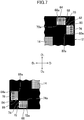
- FIG. 7 is a plan view illustrating a second modified example of the display device according to this embodiment.
- FIG. 7 illustrates only a pair of corner portions positioned on both sides of a diagonal line of the display device having a rectangular and planar shape.
- the opening portion includes a first opening portion 64 and a second opening portion 66 respectively positioned on two sides sandwiching the display region 14.
- the first opening portion 64 and the second opening portion 66 are symmetrical with respect to a point.
- the point as a reference for the point symmetry may be a center portion (intersection point of diagonal lines) of the display region 14 when the display region 14 has a rectangular shape, or may be a center portion (intersection point of diagonal lines) of the first light transmissive substrate 12 when the first light transmissive substrate 12 has a rectangular shape.
- a first main scale mark 68 and a first vernier scale mark 70 are arranged to form a pair.
- the first main scale mark 68 and the first vernier scale mark 70 are respectively arranged so that scale mark lines are aligned only in a first direction D 1 from reference scale mark lines 68a and 70a.
- a second main scale mark 72 and a second vernier scale mark 74 are arranged to form a pair.
- the second main scale mark 72 and the second vernier scale mark 74 are respectively arranged so that scale mark lines are aligned only in a second direction D 2 , which is opposite to the first direction D 1 , from reference scale mark lines 72a and 74a.
- the first main scale mark 68 and the second main scale mark 72 extend in parallel to each other
- the first vernier scale mark 70 and the second vernier scale mark 74 extend in parallel to each other.
- the first main scale mark 68 and the first vernier scale mark 70 enable measurement in the first direction D 1
- the second main scale mark 72 and the second vernier scale mark 74 enable measurement in the second direction D 2 .
- the scale marks extend only in one direction, and hence, within the first opening portion 64 or the second opening portion 66, an area occupied by the scale mark is reduced. Therefore, the sealing member 60 (see FIG. 6 ) does not cover over the scale mark, and the visibility of the scale mark is enhanced.
- the opening portion further includes a third opening portion 76 and a fourth opening portion 78 respectively positioned on two sides sandwiching the display region 14.
- the third opening portion 76 and the fourth opening portion 78 are symmetrical with respect to a point.
- the point as a reference for the point symmetry may be a center portion (intersection point of diagonal lines) of the display region 14 when the display region 14 has a rectangular shape, or may be a center portion (intersection point of diagonal lines) of the first light transmissive substrate 12 when the first light transmissive substrate 12 has a rectangular shape.
- a third main scale mark 80 and a third vernier scale mark 82 are arranged to form a pair.
- the third main scale mark 80 and the third vernier scale mark 82 are respectively arranged so that scale mark lines are aligned only in a third direction D 3 , which is orthogonal to the first direction D 1 , from reference scale mark lines 80a and 82a.
- a fourth main scale mark 84 and a fourth vernier scale mark 86 are arranged to form a pair.
- the fourth main scale mark 84 and the fourth vernier scale mark 86 are respectively arranged so that scale mark lines are aligned only in a fourth direction D 4 , which is opposite to the third direction D 3 , from reference scale mark lines 84a and 86a.
- the third main scale mark 80 and the fourth main scale mark 84 extend in parallel to each other
- the third vernier scale mark 82 and the fourth vernier scale mark 86 extend in parallel to each other.
- the third main scale mark 80 and the third vernier scale mark 82 enable measurement in the third direction D 3
- the fourth main scale mark 84 and the fourth vernier scale mark 86 enable measurement in the fourth direction D 4 .
- the measurement in the third direction D 3 and the measurement in the fourth direction D 4 can be performed. Therefore, similarly to the above-mentioned embodiment, measurement in the positive direction and in the negative direction can be performed.
- the present invention is not limited to the above-mentioned embodiment, and various modifications may be made thereto.
- the structure described in the embodiment may be replaced by substantially the same structure, a structure which has the same action and effect, or a structure which can achieve the same object.
Landscapes
- Physics & Mathematics (AREA)
- Nonlinear Science (AREA)
- Mathematical Physics (AREA)
- Chemical & Material Sciences (AREA)
- Crystallography & Structural Chemistry (AREA)
- General Physics & Mathematics (AREA)
- Optics & Photonics (AREA)
- Engineering & Computer Science (AREA)
- Microelectronics & Electronic Packaging (AREA)
- Liquid Crystal (AREA)
- Devices For Indicating Variable Information By Combining Individual Elements (AREA)
- Thin Film Transistor (AREA)
Abstract
Description
- The present invention relates to a display device.
- A liquid crystal display panel has a structure in which liquid crystal is sandwiched between a pair of substrates. One of the pair of substrates is a thin film transistor (TFT) substrate, and the other thereof is a color filter substrate. On the TFT substrate, a large number of pixel electrodes are formed, whereas, a large number of colored layers are formed on the color filter substrate. It is necessary to arrange the TFT substrate and the color filter substrate so that the pixel electrodes and the colored layers are aligned with each other. Conventionally, the liquid crystal display panel has been provided with scale marks for measuring a misalignment amount (dimension) between the TFT substrate and the color filter substrate (Japanese Patent Application Laid-open No.
Hei 10-104560 2010-102134 - Because of the formation of the scale marks, light leakage of the liquid crystal display panel has become a problem. As a countermeasure against the light leakage, there can be conceived a method of blocking off an opening through which light leaks by utilizing a metal film to be used when forming the TFT substrate. However, in this case, the metal film and the scale marks overlap one on top of another, which makes it difficult to read the scale marks. Besides, the pair of substrates are adhered to each other by a sealing member, and the liquid crystal is sealed in a space surrounded by the sealing member. Even when the sealing member overlaps the scale marks, it becomes difficult to read the scale marks. The sealing member is more liable to overlap the scale marks as the size of the region for the scale marks increases.
- The present invention has an object to provide a display device capable of preventing reduction in visibility of scale marks.
- (1) A display device according to an embodiment of the present invention includes: a first light transmissive substrate including: a display region in which an image is to be displayed in accordance with passing and blocking of light and intensity of the light; and a periphery region surrounding the display region; a light shielding portion formed in at least the periphery region of the first light transmissive substrate, the light shielding portion having an opening portion in the periphery region; a first scale mark portion formed on the first light transmissive substrate so as to be arranged inside the opening portion; a second light transmissive substrate arranged so as to overlap the first light transmissive substrate; a thin film transistor, which is formed on the second light transmissive substrate, for controlling the passing and blocking of the light and the intensity of the light; and a second scale mark portion, which is formed on the second light transmissive substrate and forms a pair with the first scale mark portion, in which: the second light transmissive substrate includes a first metal layer, a semiconductor layer, and a second metal layer which are laminated one on top of another; the thin film transistor is formed so as to include a part of the first metal layer, a part of the semiconductor layer, and a part of the second metal layer; the second scale mark portion is formed of another part of the second metal layer; under the second scale mark portion, another part of the semiconductor layer is formed so as to extend off from the second scale mark portion; and below the second scale mark portion and the semiconductor layer, another part of the first metal layer is formed in a size capable of shielding the opening portion. According to the present invention, the first metal layer shields the opening portion, and hence it is possible to prevent light leakage from the opening portion. Further, the part of the semiconductor layer is positioned so as to extend off from the second scale mark portion, which is formed of the part of the second metal layer, from below. Through absorption of light by the semiconductor layer, the second scale mark portion may be emphasized to enhance the visibility.
- (2) In the display device described in the above-mentioned item (1), the semiconductor layer may be made of amorphous silicon being a base material.
- (3) A display device according to another embodiment of the present invention includes: a first light transmissive substrate including: a display region in which an image is to be displayed in accordance with passing and blocking of light and intensity of the light; and a periphery region surrounding the display region; a light shielding portion formed in at least the periphery region of the first light transmissive substrate, the light shielding portion having an opening portion in the periphery region; a first scale mark portion formed on the first light transmissive substrate so as to be arranged inside the opening portion; a second light transmissive substrate arranged so as to overlap the first light transmissive substrate; a thin film transistor, which is formed on the second light transmissive substrate, for controlling the passing and blocking of the light and the intensity of the light; and a second scale mark portion, which is formed on the second light transmissive substrate and forms a pair with the first scale mark portion, in which: the second light transmissive substrate includes a first metal layer, a colored layer, and a second metal layer which are laminated one on top of another; the thin film transistor is formed so as to include a part of the first metal layer, a part of the colored layer, and a part of the second metal layer; the second scale mark portion is formed of another part of the second metal layer; under the second scale mark portion, another part of the colored layer is formed so as to extend off from the second scale mark portion; and below the second scale mark portion and the colored layer, another part of the first metal layer is formed in a size capable of shielding the opening portion. According to the present invention, the first metal layer shields the opening portion, and hence it is possible to prevent light leakage from the opening portion. Further, the part of the colored layer is positioned so as to extend off from the second scale mark portion, which is formed of the part of the second metal layer, from below. Through absorption of light by the colored layer, the second scale mark portion may be emphasized to enhance the visibility.
- (4) In the display device described in any one of the above-mentioned items (1) to (3), one of the first scale mark portion and the second scale mark portion may be set as a main scale mark, and another of the first scale mark portion and the second scale mark portion may be set as a vernier scale mark, to thereby enable measurement in a smaller dimension than the main scale mark.
- (5) In the display device described in the above-mentioned item (4), each of the main scale mark and the vernier scale mark may include scale mark lines which are aligned in mutually opposite directions from a reference scale mark line, to thereby enable measurement in a positive direction and in a negative direction along the scale mark lines.
- (6) In the display device described in the above-mentioned item (4), the main scale mark may include a first main scale mark and a second main scale mark extending in parallel to each other, the vernier scale mark may include a first vernier scale mark and a second vernier scale mark extending in parallel to each other, the first main scale mark and the first vernier scale mark may form a pair, the second main scale mark and the second vernier scale mark may form a pair, the opening portion may include a first opening portion and a second opening portion positioned respectively on two sides sandwiching the display region, each of the first main scale mark and the first vernier scale mark may be arranged so that, within the first opening portion, scale mark lines are aligned only in a first direction from a reference scale mark line, and each of the second main scale mark and the second vernier scale mark may be arranged so that, within the second opening portion, scale mark lines are aligned only in a second direction, which is opposite to the first direction, from a reference scale mark line.
- (7) The display device described in any one of the above-mentioned items (1) to (6) may further include: liquid crystal; a sealing member for sealing the liquid crystal between the first light transmissive substrate and the second light transmissive substrate; and a dam portion formed on the first light transmissive substrate. The sealing member may be arranged in the periphery region of the first light transmissive substrate on the display region side with respect to the opening portion of the light shielding portion, and the dam portion may be arranged between the sealing member and the opening portion so as to separate the opening portion from the sealing member.
- (8) In the display device described in the above-mentioned item (7), the dam portion may be arranged in contact with the sealing member.
- (9) A display device according to still another embodiment of the present invention includes: a first light transmissive substrate including: a display region in which an image is to be displayed in accordance with passing and blocking of light and intensity of the light; and a periphery region surrounding the display region; a light shielding portion formed in at least the periphery region of the first light transmissive substrate, the light shielding portion having an opening portion in the periphery region; a first scale mark portion formed on the first light transmissive substrate so as to be arranged inside the opening portion; a second light transmissive substrate arranged so as to overlap the first light transmissive substrate; a second scale mark portion, which is formed on the second light transmissive substrate and forms a pair with the first scale mark portion; liquid crystal; a sealing member for sealing the liquid crystal between the first light transmissive substrate and the second light transmissive substrate; and a dam portion formed on the first light transmissive substrate, in which: the sealing member is arranged in the periphery region of the first light transmissive substrate on the display region side with respect to the opening portion of the light shielding portion; and the dam portion is arranged between the sealing member and the opening portion so as to separate the opening portion from the sealing member. According to the present invention, with the dam portion, it is possible to prevent the opening portion from being covered with the sealing member. In this manner, it is possible to prevent reduction in visibility of the first scale mark portion and the second scale mark portion.
- (10) A display device according to yet another embodiment of the present invention includes: a first light transmissive substrate including: a display region in which an image is to be displayed in accordance with passing and blocking of light and intensity of the light; and a periphery region surrounding the display region; a light shielding portion formed in at least the periphery region of the first light transmissive substrate, the light shielding portion including a first opening portion and a second opening portion positioned respectively on two sides of the periphery region, which sandwich the display region; a first scale mark portion formed on the first light transmissive substrate so as to be arranged inside the first opening portion; a second scale mark portion formed on the first light transmissive substrate so as to be arranged inside the second opening portion; a second light transmissive substrate arranged so as to overlap the first light transmissive substrate; a third scale mark portion, which is formed on the second light transmissive substrate and forms a pair with the first scale mark portion; and a fourth scale mark portion, which is formed on the second light transmissive substrate and forms a pair with the second scale mark portion, in which: one of the first scale mark portion and the third scale mark portion is set as a first main scale mark, and another of the first scale mark portion and the third scale mark portion is set as a first vernier scale mark, to thereby enable measurement in a smaller dimension than the first main scale mark; one of the second scale mark portion and the fourth scale mark portion is set as a second main scale mark, and another of the second scale mark portion and the fourth scale mark portion is set as a second vernier scale mark, to thereby enable measurement in a smaller dimension than the second main scale mark; the first main scale mark and the second main scale mark extend in parallel to each other; the first vernier scale mark and the second vernier scale mark extend in parallel to each other; each of the first main scale mark and the first vernier scale mark is arranged so that, within the first openingportion, scale mark lines are aligned only in a first direction from a reference scale mark line; and each of the second main scale mark and the second vernier scale mark is arranged so that, within the second opening portion, scale mark lines are aligned only in a second direction, which is opposite to the first direction, from a reference scale mark line. According to the present invention, the scale mark extends only in one direction, and hence, within the opening portion, an area occupied by the scale mark is reduced. Therefore, the visibility is enhanced.
- In the accompanying drawings:
-
FIG. 1 is a plan view illustrating a display device according to an embodiment of the present invention; -
FIG. 2 is an enlarged view of a corner portion of the display device illustrated inFIG. 1 ; -
FIG. 3 is a sectional view taken along the line III-III of the display device illustrated inFIG. 2 ; -
FIG. 4 is a sectional view of the display device at a position different from that ofFIG. 3 ; -
FIG. 5 is a view illustrating a first modified example of the display device according to the embodiment; -
FIG. 6 is a sectional view taken along the line VI-VI of the display device illustrated inFIG. 5 ; and -
FIG. 7 is a plan view illustrating a second modified example of the display device according to the embodiment. - Hereinafter, an embodiment of the present invention is described with reference to the drawings.
-
FIG. 1 is a plan view illustrating a display device according to the embodiment of the present invention.FIG. 2 is an enlarged view of a corner portion of the display device illustrated inFIG. 1 .FIG. 3 is a sectional view taken along the line III-III of the display device illustrated inFIG. 2 . - The display device according to this embodiment is a liquid crystal display device, and hence includes
liquid crystal 10 illustrated inFIG. 3 . By controlling the direction of molecules of theliquid crystal 10, passing and blocking of light and intensity of the light may be controlled. - The display device includes a first light transmissive substrate 12 (for example, glass substrate). The first light
transmissive substrate 12 includes, as illustrated inFIG. 1 , adisplay region 14 in which an image is to be displayed. The image is formed of a plurality of (large number of) pixels (not shown), and is displayed in accordance with the passing and blocking of the light and the intensity of the light controlled in each pixel. That is, by controlling theliquid crystal 10, the image formed by the light is displayed. Aperiphery region 16 is provided so as to surround thedisplay region 14. - In at least the
periphery region 16 of the first lighttransmissive substrate 12, alight shielding portion 18 is formed. Thelight shielding portion 18 blocks light passage. In this manner, theperiphery region 16 surrounding thedisplay region 14 is darkened, to thereby make the image more visible. Thelight shielding portion 18 includes, as illustrated inFIG. 2 , ablack matrix 20 arranged in thedisplay region 14. Thelight shielding portion 18 has openingportions 22 in theperiphery region 16. Light passes through the openingportions 22. Further, a firstscale mark portion 24 is formed on the firstlight transmissive substrate 12 so as to be arranged inside each openingportion 22. The firstscale mark portion 24 blocks light passage. A plurality of scale mark lines 26 are aligned to form the firstscale mark portion 24. As illustrated inFIG. 2 , one of the plurality of scale mark lines 26 corresponds to a referencescale mark line 28. A line positioned at the center of the plurality of scale mark lines 26 of the firstscale mark portion 24 corresponds to the referencescale mark line 28. The scale mark lines 26 are aligned in mutually opposite directions from the referencescale mark line 28 so that measurement in a positive direction and in a negative direction can be performed along the scale mark lines. Thelight shielding portion 18 and the firstscale mark portion 24 are made of the same material. - As illustrated in
FIG. 3 , the firstlight transmissive substrate 12 includes acolor filter layer 30. Thecolor filter layer 30 is formed so as to cover thelight shielding portion 18. Thecolor filter layer 30 also covers the openingportion 22, and further covers the firstscale mark portion 24. - The display device includes a second light transmissive substrate 32 (for example, glass substrate) which is arranged so as to overlap the first
light transmissive substrate 12. Theliquid crystal 10 is sandwiched between the firstlight transmissive substrate 12 and the secondlight transmissive substrate 32. Note that, illustration of alignment films is omitted. - On the second
light transmissive substrate 32, afirst metal layer 34, asemiconductor layer 36, and asecond metal layer 38 are laminated in the stated order from the lower side (secondlight transmissive substrate 32 side). "Laminate" means that layers are partially overlapped one on top of another. Therefore, there may be overlapping portions and non-overlapping portions in the layers, and another layer may be interposed between the layers. In the example illustrated inFIG. 3 , an insulatinglayer 40 is interposed between thefirst metal layer 34 and thesemiconductor layer 36. Further, apassivation film 42 is formed on thesecond metal layer 38. Thepassivation film 42 covers thesemiconductor layer 36 and also thesecond metal layer 38, and further covers the insulatinglayer 40. - The
first metal layer 34 and thesecond metal layer 38 are each made of a metal such as aluminum, molybdenum, and chromium. Thefirst metal layer 34 and thesecond metal layer 38 are often made of the same material, and in this case, a light reflectance ratio is the same. Therefore, thefirst metal layer 34 and thesecond metal layer 38, which partially overlap one on top of another so that ends thereof are offset from each other, are visually indistinguishable when viewed from the surface side. - The
semiconductor layer 36 is made of amorphous silicon being a base material. The amorphous silicon has a red color, and hence thesemiconductor layer 36 may be used as the colored layer. The semiconductor layer 36 (colored layer) and thesecond metal layer 38 have different light reflectance ratios or different colors, and hence thesecond metal layer 38 and thesemiconductor layer 36, which partially overlap one on top of another so that ends thereof are offset from each other, are easily distinguishable when viewed from the surface side. - As illustrated in
FIG. 3 , on the secondlight transmissive substrate 32, a secondscale mark portion 44 which forms a pair with the firstscale mark portion 24 is formed. As illustrated inFIG. 2 , a plurality of scale mark lines 46 are aligned to form the secondscale mark portion 44. One of the plurality of scale mark lines 46 corresponds to a referencescale mark line 48. A line positioned at the center of the plurality of scale mark lines 46 of the secondscale mark portion 44 corresponds to the referencescale mark line 48. The scale mark lines 46 are aligned in mutually opposite directions from the referencescale mark line 48 so that measurement in a positive direction and in a negative direction can be performed along the scale mark lines. - In this embodiment, the first
scale mark portion 24 is a main scale mark, and the secondscale mark portion 44 is a vernier scale mark. Intervals between the scale mark lines 46 of the secondscale mark portion 44 is smaller than intervals between the scale mark lines 26 of the firstscale mark portion 24. By reading the scale mark line 46 of the secondscale mark portion 44, which coincides with the firstscale mark portion 24, it is possible to measure a smaller dimension than the firstscale mark portion 24 which is the main scale mark. Note that, as a modified example, the secondscale mark portion 44 may be the main scale mark, and the firstscale mark portion 24 may be the vernier scale mark. - The second
scale mark portion 44 is formed of a part of thesecond metal layer 38. Under the secondscale mark portion 44, a part of the semiconductor layer 36 (colored layer) is formed so as to extend off from the secondscale mark portion 44. The semiconductor layer 36 (colored layer) extends off from the secondscale mark portion 44 so as to surround the entire outer periphery of the secondscale mark portion 44. Therefore, through absorption of light by the semiconductor layer 36 (colored layer), the secondscale mark portion 44 may be emphasized to enhance the visibility. - Below the second
scale mark portion 44 and thesemiconductor layer 36, a part of thefirst metal layer 34 is formed in a size capable of shielding the openingportion 22. Thefirst metal layer 34 shields the openingportion 22, and hence it is possible to prevent the light leakage from the openingportion 22 of thelight shielding portion 18. -
FIG. 4 is a sectional view of the display device at a position different from that ofFIG. 3 . On the secondlight transmissive substrate 32, there is formed athin film transistor 50 for controlling passing and blocking of light and intensity of the light. Thethin film transistor 50 is formed so as to include a part of the first metal layer 34 (for example, gate electrode 52), a part of the semiconductor layer 36 (for example, channel region 54), and a part of the second metal layer 38 (for example,drain electrode 56 and source electrode 58) . The insulating layer 40 (gate insulating film) is interposed between thefirst metal layer 34 forming thegate electrode 52 and thesemiconductor layer 36 forming thechannel region 54. - In this embodiment, the
first metal layer 34 includes a portion shielding the openingportion 22 and a portion forming a part of the thin film transistor 50 (for example, the gate electrode 52). Thesecond metal layer 38 includes a portion forming the secondscale mark portion 44 and a portion forming a part of the thin film transistor 50 (for example, thedrain electrode 56 and the source electrode 58). The semiconductor layer 36 (colored layer) includes a portion which extends off from the secondscale mark portion 44 from below, and a portion forming a part of the thin film transistor 50 (for example, the channel region 54). Therefore, the secondscale mark portion 44 and thethin film transistor 50 can be formed of the samefirst metal layer 34,second metal layer 38, andsemiconductor layer 36, and hence the number of the manufacturing steps does not increase. -
FIG. 5 is a view illustrating a first modified example of the display device according to this embodiment.FIG. 6 is a sectional view taken along the line VI-VI of the display device illustrated inFIG. 5 . In this example, theliquid crystal 10 is sealed between the firstlight transmissive substrate 12 and the secondlight transmissive substrate 32 by a sealingmember 60. - The sealing
member 60 is arranged in theperiphery region 16 of the firstlight transmissive substrate 12 on thedisplay region 14 side with respect to the openingportion 22 of thelight shielding portion 18. The sealingmember 60 is provided in close contact with mutually facing surfaces of the firstlight transmissive substrate 12 and the secondlight transmissive substrate 32. - On the first
light transmissive substrate 12, adam portion 62 is formed. Thedam portion 62 is arranged between the openingportion 22 and thedisplay region 14. For example, thedam portion 62 is positioned adjacent to the openingportion 22 on thedisplay region 14 side. Further, thedam portion 62 is arranged between the sealingmember 60 and the openingportion 22 so as to separate theopening portion 22 from the sealingmember 60. - Specifically, the sealing
member 60 is formed by arranging and curing a resin precursor between the firstlight transmissive substrate 12 and the secondlight transmissive substrate 32. In this process, the resin precursor becomes a liquid or paste, and hence when the firstlight transmissive substrate 12 and the secondlight transmissive substrate 32 are pressed so as to narrow a gap therebetween, the resin precursor attempts to expand in a direction toward the openingportion 22. In this context, thedam portion 62 plays a role to stop the resin precursor right before the openingportion 22. With thedam portion 62, it is possible to prevent theopening portion 22 from being covered with the sealingmember 60. In this manner, it is possible to prevent reduction in visibility of the firstscale mark portion 24 and the secondscale mark portion 44. - The
dam portion 62 is arranged in contact with the sealingmember 60. Further, thedam portion 62 is arranged in contact (close contact) with the firstlight transmissive substrate 12. In the example ofFIG. 6 , thedam portion 62 is not provided in contact with the secondlight transmissive substrate 32, and there is a gap therebetween. Even in this case, because thedam portion 62 is provided, flow resistance of the resin precursor can be enhanced, and hence it is possible to impede the progress of the resin precursor. As a modified example, thedam portion 62 may be arranged in contact (close contact) with the firstlight transmissive substrate 12 and the secondlight transmissive substrate 32. For example, thedam portion 62 may be formed on the firstlight transmissive substrate 12 in advance, and when the firstlight transmissive substrate 12 is adhered to the secondlight transmissive substrate 32, thedam portion 62 may be pressed against the secondlight transmissive substrate 32. -
FIG. 7 is a plan view illustrating a second modified example of the display device according to this embodiment.FIG. 7 illustrates only a pair of corner portions positioned on both sides of a diagonal line of the display device having a rectangular and planar shape. - In this example, the opening portion includes a
first opening portion 64 and asecond opening portion 66 respectively positioned on two sides sandwiching thedisplay region 14. Thefirst opening portion 64 and thesecond opening portion 66 are symmetrical with respect to a point. The point as a reference for the point symmetry may be a center portion (intersection point of diagonal lines) of thedisplay region 14 when thedisplay region 14 has a rectangular shape, or may be a center portion (intersection point of diagonal lines) of the firstlight transmissive substrate 12 when the firstlight transmissive substrate 12 has a rectangular shape. - Inside the
first opening portion 64, a firstmain scale mark 68 and a firstvernier scale mark 70 are arranged to form a pair. The firstmain scale mark 68 and the firstvernier scale mark 70 are respectively arranged so that scale mark lines are aligned only in a first direction D1 from referencescale mark lines - Inside the
second opening portion 66, a secondmain scale mark 72 and a secondvernier scale mark 74 are arranged to form a pair. The secondmain scale mark 72 and the secondvernier scale mark 74 are respectively arranged so that scale mark lines are aligned only in a second direction D2, which is opposite to the first direction D1, from referencescale mark lines main scale mark 68 and the secondmain scale mark 72 extend in parallel to each other, and the firstvernier scale mark 70 and the secondvernier scale mark 74 extend in parallel to each other. - The first
main scale mark 68 and the firstvernier scale mark 70 enable measurement in the first direction D1, and the secondmain scale mark 72 and the secondvernier scale mark 74 enable measurement in the second direction D2. As described above, the scale marks extend only in one direction, and hence, within thefirst opening portion 64 or thesecond opening portion 66, an area occupied by the scale mark is reduced. Therefore, the sealing member 60 (seeFIG. 6 ) does not cover over the scale mark, and the visibility of the scale mark is enhanced. - Further, in the example of
FIG. 7 , the opening portion further includes athird opening portion 76 and afourth opening portion 78 respectively positioned on two sides sandwiching thedisplay region 14. Thethird opening portion 76 and thefourth opening portion 78 are symmetrical with respect to a point. The point as a reference for the point symmetry may be a center portion (intersection point of diagonal lines) of thedisplay region 14 when thedisplay region 14 has a rectangular shape, or may be a center portion (intersection point of diagonal lines) of the firstlight transmissive substrate 12 when the firstlight transmissive substrate 12 has a rectangular shape. - Inside the
third opening portion 76, a thirdmain scale mark 80 and a thirdvernier scale mark 82 are arranged to form a pair. The thirdmain scale mark 80 and the thirdvernier scale mark 82 are respectively arranged so that scale mark lines are aligned only in a third direction D3, which is orthogonal to the first direction D1, from referencescale mark lines - Inside the
fourth opening portion 78, a fourthmain scale mark 84 and a fourthvernier scale mark 86 are arranged to form a pair. The fourthmain scale mark 84 and the fourthvernier scale mark 86 are respectively arranged so that scale mark lines are aligned only in a fourth direction D4, which is opposite to the third direction D3, from referencescale mark lines main scale mark 80 and the fourthmain scale mark 84 extend in parallel to each other, and the thirdvernier scale mark 82 and the fourthvernier scale mark 86 extend in parallel to each other. - The third
main scale mark 80 and the thirdvernier scale mark 82 enable measurement in the third direction D3, and the fourthmain scale mark 84 and the fourthvernier scale mark 86 enable measurement in the fourth direction D4. - Therefore, in addition to the measurement in the first direction D1 and the measurement in the second direction D2 as described above, the measurement in the third direction D3 and the measurement in the fourth direction D4 can be performed. Therefore, similarly to the above-mentioned embodiment, measurement in the positive direction and in the negative direction can be performed.
- The present invention is not limited to the above-mentioned embodiment, and various modifications may be made thereto. For example, the structure described in the embodiment may be replaced by substantially the same structure, a structure which has the same action and effect, or a structure which can achieve the same object.
- The above embodiments of the invention as well as the appended claims and figures show multiple characterizing features of the invention in specific combinations. The skilled person will easily be able to consider further combinations or sub-combinations of these features in order to adapt the invention as defined in the in the claims to his specific needs.
Claims (10)
- A display device, comprising:a first light transmissive substrate (12) comprising:a display region (14) in which an image is to be displayed in accordance with passing and blocking of light and intensity of the light; anda periphery region (16) surrounding the display region (14) ; a light shieldingportion formed in at least the periphery region (16) of the first light transmissive substrate (12), the light shielding portion (18) having an opening portion (22) in the periphery region (16);a first scale mark portion (24) formed on the first light transmissive substrate (12) so as to be arranged inside the opening portion (22);a second light transmissive substrate (32) arranged so as to overlap the first light transmissive substrate (12);a thin film transistor (50), which is formed on the second light transmissive substrate (32), for controlling the passing and blocking of the light and the intensity of the light; anda second scale mark portion (44), which is formed on the second light transmissive substrate (32) and forms a pair with the first scale mark portion (24), wherein:the second light transmissive substrate (32) includes a first metal layer (34), a semiconductor layer (36), and a second metal layer (38) which are laminated one on top of another;the thin film transistor (50) is formed so as to include a part of the first metal layer (34), a part of the semiconductor layer (36), and a part of the second metal layer (38);the second scale mark portion (44) is formed of another part of the second metal layer (38);under the second scale mark portion (44), another part of the semiconductor layer (36) is formed so as to extend off from the second scale mark portion (44); andbelow the second scale mark portion (44) and the semiconductor layer (36), another part of the first metal layer (34) is formed in a size capable of shielding the opening portion (22).
- The display device according to claim 1, wherein the semiconductor layer (36) is made of amorphous silicon being a base material.
- A display device, comprising:a first light transmissive substrate (12) comprising:a display region (14) in which an image is to be displayed in accordance with passing and blocking of light and intensity of the light; anda periphery region (16) surrounding the display region (14); a light shielding portion (18) formed in at least the periphery region (16) of the first light transmissive substrate (12), the light shielding portion (18) having an opening portion (22) in the periphery region (16);a first scale mark portion (24) formed on the first light transmissive substrate (12) so as to be arranged inside the opening portion (22);a second light transmissive substrate (32) arranged so as to overlap the first light transmissive substrate (12);a thin film transistor (50), which is formed on the second light transmissive substrate (32), for controlling the passing and blocking of the light and the intensity of the light; anda second scale mark portion (44), which is formed on the second light transmissive substrate (23) and forms a pair with the first scale mark portion (24), wherein:the second light transmissive substrate (32) includes a first metal layer (34), a colored layer (36), and a second metal layer (38) which are laminated one on top of another;the thin film transistor (50) is formed so as to include a part of the first metal layer (34), a part of the colored layer (36), and a part of the second metal layer (38);the second scale mark portion (44) is formed of another part of the second metal layer (38);under the second scale mark portion (44), another part of the colored layer (36) is formed so as to extend off from the second scale mark portion (44); andbelow the second scale mark portion (44) and the colored layer (36), another part of the first metal layer (34) is formed in a size capable of shielding the opening portion (22).
- The display device according to any one of claims 1 to 3, wherein one of the first scale mark portion (24) and the second scale mark portion (44) is set as a main scale mark, and another of the first scale mark portion (24) and the second scale mark portion (44) is set as a vernier scale mark, to thereby enable measurement in a smaller dimension than the main scale mark.
- The display device according to claim 4, wherein each of the main scale mark (68, 72) and the vernier scale mark (70, 74) includes scale mark lines which are aligned in mutually opposite directions from a reference scale mark line, to thereby enable measurement in a positive direction and in a negative direction along the scale mark lines.
- The display device according to claim 4, wherein:the main scale mark comprises a first main scale mark (68) and a second main scale mark (72) extending in parallel to each other;the vernier scale mark comprises a first vernier scale mark (70) and a second vernier scale mark (74) extending in parallel to each other;the first main scale mark (68) and the first vernier scale mark (70) form a pair;the second main scale mark (72) and the second vernier scale mark (74) form a pair;the opening portion (22) comprises a first opening portion (64) and a second opening portion (66) positioned respectively on two sides sandwiching the display region (14);each of the first main scale mark (68) and the first vernier scale mark (70) is arranged so that, within the first opening portion (64), scale mark lines are aligned only in a first direction (D1) from a reference scale mark line (68a, 70a); andeach of the second main scale mark (72) and the second vernier scale mark (74) is arranged so that, within the second opening portion (66), scale mark lines are aligned only in a second direction (D2), which is opposite to the first direction (D1), from a reference scale mark line (72a, 74a).
- The display device according to any one of claims 1 to 6, further comprising:liquid crystal (10);a sealing member (60) for sealing the liquid crystal (10) between the first light transmissive substrate (12) and the second light transmissive substrate (32); anda dam portion (62) formed on the first light transmissive substrate (12), wherein:the sealing member (60) is arranged in the periphery region (16) of the first light transmissive substrate (12) on the display region side with respect to the opening portion (22) of the light shielding portion (18); andthe dam portion (62) is arranged between the sealing member (60) and the opening portion (22) so as to separate the opening portion (22) from the sealing member (60).
- The display device according to claim 7, wherein the dam portion (62) is arranged in contact with the sealing member (60).
- A display device, comprising:a first light transmissive substrate (12) comprising:a display region (14) in which an image is to be displayed in accordance with passing and blocking of light and intensity of the light; anda periphery region (16) surrounding the display region (14);a light shielding portion (18) formed in at least the periphery region (16) of the first light transmissive substrate (12), the light shielding portion (18) having an opening portion (22) in the periphery region (16);a first scale mark portion (24) formed on the first light transmissive substrate (12) so as to be arranged inside the opening portion (22);a second light transmissive substrate (32) arranged so as to overlap the first light transmissive substrate (12);a second scale mark portion (44), which is formed on the second light transmissive substrate (32) and forms a pair with the first scale mark portion (24);liquid crystal (10);a sealing member (60) for sealing the liquid crystal (10) between the first light transmissive substrate (12) and the second light transmissive substrate (32); anda dam portion (62) formed on the first light transmissive substrate (12), wherein:the sealing member (60) is arranged in the periphery region (16) of the first light transmissive substrate (12) on the display region side with respect to the opening portion (22) of the light shielding portion (18); andthe dam portion (62) is arranged between the sealing member (60) and the opening portion (22) so as to separate the opening portion from the sealing member (60).
- A display device, comprising:a first light transmissive substrate (12) comprising:a display region (14) in which an image is to be displayed in accordance with passing and blocking of light and intensity of the light; anda periphery region (16) surrounding the display region (14);a light shielding portion (18) formed in at least the periphery region (16) of the first light transmissive substrate (12), the light shielding portion (18) comprising a first opening portion (64) and a second opening portion (66) positioned respectively on two sides of the periphery region (16), which sandwich the display region (14);a first scale mark portion (68) formed on the first light transmissive substrate (12) so as to be arranged inside the first opening portion (64);a second scale mark portion (72) formed on the first light transmissive substrate (12) so as to be arranged inside the second opening portion (66);a second light transmissive substrate (32) arranged so as to overlap the first light transmissive substrate (12);a third scale mark portion (70), which is formed on the second light transmissive substrate (32) and forms a pair with the first scale mark portion (68); anda fourth scale mark portion (74), which is formed on the second light transmissive substrate (32) and forms a pair with the second scale mark portion (72), wherein:one of the first scale mark portion (68) and the third scale mark portion (70) is set as a first main scale mark, and another of the first scale mark portion (68) and the third scale mark portion (70) is set as a first vernier scale mark, to thereby enable measurement in a smaller dimension than the first main scale mark;one of the second scale mark portion (72) and the fourth scale mark portion (74) is set as a second main scale mark, and another of the second scale mark portion (72) and the fourth scale mark portion (74) is set as a second vernier scale mark, to thereby enable measurement in a smaller dimension than the second main scale mark;the first main scale mark and the second main scale mark extend in parallel to each other;the first vernier scale mark and the second vernier scale mark extend in parallel to each other;each of the first main scale mark and the first vernier scale mark is arranged so that, within the first opening portion (64), scale mark lines are aligned only in a first direction (D1) from a reference scale mark line (68a, 70a); andeach of the second main scale mark and the second vernier scale mark is arranged so that, within the second opening portion (66), scale mark lines are aligned only in a second direction (D2), which is opposite to the first direction (D1), from a reference scale mark line (72a, 74a).
Applications Claiming Priority (1)
| Application Number | Priority Date | Filing Date | Title |
|---|---|---|---|
| JP2011025574A JP5302345B2 (en) | 2011-02-09 | 2011-02-09 | Display device |
Publications (3)
| Publication Number | Publication Date |
|---|---|
| EP2487527A2 true EP2487527A2 (en) | 2012-08-15 |
| EP2487527A3 EP2487527A3 (en) | 2013-03-27 |
| EP2487527B1 EP2487527B1 (en) | 2014-07-23 |
Family
ID=45562881
Family Applications (1)
| Application Number | Title | Priority Date | Filing Date |
|---|---|---|---|
| EP20120154468 Active EP2487527B1 (en) | 2011-02-09 | 2012-02-08 | Display device |
Country Status (6)
| Country | Link |
|---|---|
| US (4) | US8760612B2 (en) |
| EP (1) | EP2487527B1 (en) |
| JP (1) | JP5302345B2 (en) |
| KR (1) | KR101317557B1 (en) |
| CN (1) | CN102636903B (en) |
| TW (1) | TWI479228B (en) |
Families Citing this family (15)
| Publication number | Priority date | Publication date | Assignee | Title |
|---|---|---|---|---|
| JP2013225033A (en) * | 2012-04-23 | 2013-10-31 | Japan Display Inc | Display device and method of manufacturing the same |
| KR20140024572A (en) * | 2012-08-20 | 2014-03-03 | 삼성디스플레이 주식회사 | Display panel |
| CN205539837U (en) * | 2016-04-15 | 2016-08-31 | 京东方科技集团股份有限公司 | Liquid crystal display panel and display device |
| WO2018010727A1 (en) * | 2016-07-12 | 2018-01-18 | Dynamic Solar Systems Ag | Room temperature printing method for producing a pv layer sequence and pv layer sequence obtained using the method |
| CN106094311B (en) * | 2016-08-22 | 2019-09-06 | 武汉华星光电技术有限公司 | A kind of narrow frame liquid crystal display panel and its production method for organizing day-mark ruler |
| CN107844001B (en) * | 2017-09-04 | 2020-07-24 | 深圳市华星光电技术有限公司 | Display panel |
| JP2019124733A (en) * | 2018-01-12 | 2019-07-25 | パナソニック液晶ディスプレイ株式会社 | Liquid crystal display device |
| JP2019124734A (en) | 2018-01-12 | 2019-07-25 | パナソニック液晶ディスプレイ株式会社 | Method for manufacturing liquid crystal display device |
| CN108363228B (en) * | 2018-02-09 | 2021-09-28 | 厦门天马微电子有限公司 | Array substrate, display panel and method for determining cutting line |
| CN110275333B (en) * | 2018-03-14 | 2022-11-25 | 群创光电股份有限公司 | Display device and its manufacturing method |
| JP2019191239A (en) * | 2018-04-19 | 2019-10-31 | シャープ株式会社 | Display panel |
| CN111261063B (en) | 2020-03-31 | 2021-07-06 | 深圳市华星光电半导体显示技术有限公司 | Display panel and display device |
| KR102909039B1 (en) | 2020-07-06 | 2026-01-07 | 삼성디스플레이 주식회사 | Display panel and mask sheet for manufacturing the same |
| KR102946175B1 (en) * | 2021-10-07 | 2026-03-31 | 삼성디스플레이 주식회사 | Display panel and method for fabricating the same |
| KR20230090405A (en) * | 2021-12-14 | 2023-06-22 | 삼성디스플레이 주식회사 | Display device |
Citations (2)
| Publication number | Priority date | Publication date | Assignee | Title |
|---|---|---|---|---|
| JPH10104560A (en) | 1996-09-27 | 1998-04-24 | Sharp Corp | Liquid crystal display device and manufacturing method thereof |
| JP2010102134A (en) | 2008-10-24 | 2010-05-06 | Hitachi Displays Ltd | Liquid crystal display device |
Family Cites Families (13)
| Publication number | Priority date | Publication date | Assignee | Title |
|---|---|---|---|---|
| JP3766132B2 (en) * | 1996-02-27 | 2006-04-12 | シャープ株式会社 | Display panel |
| JP4154086B2 (en) * | 1999-07-29 | 2008-09-24 | 日立化成工業株式会社 | Photosensitive polymer composition, pattern manufacturing method and electronic component |
| JP2001175198A (en) * | 1999-12-14 | 2001-06-29 | Semiconductor Energy Lab Co Ltd | Semiconductor device and manufacturing method thereof |
| JP2002072222A (en) * | 2000-08-23 | 2002-03-12 | Toshiba Corp | Liquid crystal display device and method of manufacturing liquid crystal display device |
| JP2004347659A (en) | 2003-05-20 | 2004-12-09 | Sony Corp | Liquid crystal panel, manufacturing method thereof, and liquid crystal display device |
| KR101009668B1 (en) * | 2003-10-06 | 2011-01-19 | 엘지디스플레이 주식회사 | LCD and its manufacturing method |
| KR101026982B1 (en) * | 2004-06-03 | 2011-04-11 | 엘지디스플레이 주식회사 | Array Substrate for LCD and Manufacturing Method |
| KR101183374B1 (en) * | 2005-06-27 | 2012-09-21 | 엘지디스플레이 주식회사 | Liquid crystal display device and method of lcd thereof |
| CN101233554B (en) | 2005-09-15 | 2010-08-18 | 夏普株式会社 | Display panel |
| US7916247B2 (en) * | 2007-08-30 | 2011-03-29 | Seiko Epson Corporation | Electro-optic device, and electronic apparatus including the same |
| JP5104176B2 (en) | 2007-10-04 | 2012-12-19 | セイコーエプソン株式会社 | Electro-optical device and electronic apparatus |
| JP2009192667A (en) | 2008-02-13 | 2009-08-27 | Epson Imaging Devices Corp | Display device and method for manufacturing display device |
| JP5502508B2 (en) | 2010-01-27 | 2014-05-28 | 株式会社ジャパンディスプレイ | Liquid crystal display device and electronic device |
-
2011
- 2011-02-09 JP JP2011025574A patent/JP5302345B2/en active Active
-
2012
- 2012-01-16 TW TW101101630A patent/TWI479228B/en active
- 2012-02-06 US US13/366,400 patent/US8760612B2/en active Active
- 2012-02-08 CN CN201210029621.3A patent/CN102636903B/en active Active
- 2012-02-08 EP EP20120154468 patent/EP2487527B1/en active Active
- 2012-02-08 KR KR20120012991A patent/KR101317557B1/en active Active
-
2014
- 2014-06-09 US US14/299,669 patent/US8958047B2/en active Active
-
2015
- 2015-01-08 US US14/592,496 patent/US9274366B2/en active Active
- 2015-10-07 US US14/877,731 patent/US9417476B2/en active Active
Patent Citations (2)
| Publication number | Priority date | Publication date | Assignee | Title |
|---|---|---|---|---|
| JPH10104560A (en) | 1996-09-27 | 1998-04-24 | Sharp Corp | Liquid crystal display device and manufacturing method thereof |
| JP2010102134A (en) | 2008-10-24 | 2010-05-06 | Hitachi Displays Ltd | Liquid crystal display device |
Also Published As
| Publication number | Publication date |
|---|---|
| EP2487527A3 (en) | 2013-03-27 |
| JP2012163871A (en) | 2012-08-30 |
| CN102636903B (en) | 2015-08-26 |
| JP5302345B2 (en) | 2013-10-02 |
| US20150116642A1 (en) | 2015-04-30 |
| KR101317557B1 (en) | 2013-10-11 |
| US20140285756A1 (en) | 2014-09-25 |
| TW201235737A (en) | 2012-09-01 |
| US20160026036A1 (en) | 2016-01-28 |
| TWI479228B (en) | 2015-04-01 |
| EP2487527B1 (en) | 2014-07-23 |
| KR20120092051A (en) | 2012-08-20 |
| US8760612B2 (en) | 2014-06-24 |
| US8958047B2 (en) | 2015-02-17 |
| CN102636903A (en) | 2012-08-15 |
| US9417476B2 (en) | 2016-08-16 |
| US9274366B2 (en) | 2016-03-01 |
| US20120200820A1 (en) | 2012-08-09 |
Similar Documents
| Publication | Publication Date | Title |
|---|---|---|
| EP2487527B1 (en) | Display device | |
| JP5523864B2 (en) | Liquid crystal display | |
| US9097926B2 (en) | Substrate of display device, display device and manufacturing method for display panel | |
| US11460734B2 (en) | Display device | |
| JP5856006B2 (en) | LCD panel | |
| US20150370105A1 (en) | Liquid crystal display including light blocking member overlapping spacer | |
| CN104407475A (en) | Liquid crystal display panel | |
| US20170299916A1 (en) | Liquid crystal display device | |
| CN106646966A (en) | Display device | |
| US20160223855A1 (en) | Liquid-crystal display device and a manufacturing method of it | |
| CN102169262B (en) | Display panels and electronic equipment | |
| JP5879384B2 (en) | Liquid crystal display | |
| US9128330B2 (en) | Liquid crystal display device and method of manufacturing the same | |
| JP5615962B2 (en) | Display device | |
| CN210123505U (en) | Liquid crystal display device having a plurality of pixel electrodes | |
| JP2019159154A (en) | Display device | |
| JP2006330169A (en) | Color filter substrate and manufacturing method thereof | |
| JP2008089674A (en) | Liquid crystal display |
Legal Events
| Date | Code | Title | Description |
|---|---|---|---|
| PUAI | Public reference made under article 153(3) epc to a published international application that has entered the european phase |
Free format text: ORIGINAL CODE: 0009012 |
|
| 17P | Request for examination filed |
Effective date: 20120313 |
|
| AK | Designated contracting states |
Kind code of ref document: A2 Designated state(s): AL AT BE BG CH CY CZ DE DK EE ES FI FR GB GR HR HU IE IS IT LI LT LU LV MC MK MT NL NO PL PT RO RS SE SI SK SM TR |
|
| AX | Request for extension of the european patent |
Extension state: BA ME |
|
| RIC1 | Information provided on ipc code assigned before grant |
Ipc: G02F 1/1333 20060101AFI20121016BHEP Ipc: G02F 1/1362 20060101ALI20121016BHEP |
|
| PUAL | Search report despatched |
Free format text: ORIGINAL CODE: 0009013 |
|
| AK | Designated contracting states |
Kind code of ref document: A3 Designated state(s): AL AT BE BG CH CY CZ DE DK EE ES FI FR GB GR HR HU IE IS IT LI LT LU LV MC MK MT NL NO PL PT RO RS SE SI SK SM TR |
|
| AX | Request for extension of the european patent |
Extension state: BA ME |
|
| RIC1 | Information provided on ipc code assigned before grant |
Ipc: G02F 1/1362 20060101ALI20130220BHEP Ipc: G02F 1/1333 20060101AFI20130220BHEP |
|
| REG | Reference to a national code |
Ref country code: DE Ref legal event code: R079 Ref document number: 602012002472 Country of ref document: DE Free format text: PREVIOUS MAIN CLASS: G02F0001133300 Ipc: G02F0001136800 |
|
| GRAP | Despatch of communication of intention to grant a patent |
Free format text: ORIGINAL CODE: EPIDOSNIGR1 |
|
| RIC1 | Information provided on ipc code assigned before grant |
Ipc: G02F 1/1368 20060101AFI20140304BHEP Ipc: G02F 1/1333 20060101ALI20140304BHEP Ipc: G02F 1/1362 20060101ALI20140304BHEP |
|
| INTG | Intention to grant announced |
Effective date: 20140321 |
|
| RAP1 | Party data changed (applicant data changed or rights of an application transferred) |
Owner name: JAPAN DISPLAY INC. |
|
| GRAS | Grant fee paid |
Free format text: ORIGINAL CODE: EPIDOSNIGR3 |
|
| GRAA | (expected) grant |
Free format text: ORIGINAL CODE: 0009210 |
|
| AK | Designated contracting states |
Kind code of ref document: B1 Designated state(s): AL AT BE BG CH CY CZ DE DK EE ES FI FR GB GR HR HU IE IS IT LI LT LU LV MC MK MT NL NO PL PT RO RS SE SI SK SM TR |
|
| REG | Reference to a national code |
Ref country code: GB Ref legal event code: FG4D |
|
| REG | Reference to a national code |
Ref country code: CH Ref legal event code: EP |
|
| REG | Reference to a national code |
Ref country code: IE Ref legal event code: FG4D |
|
| REG | Reference to a national code |
Ref country code: AT Ref legal event code: REF Ref document number: 679175 Country of ref document: AT Kind code of ref document: T Effective date: 20140815 |
|
| REG | Reference to a national code |
Ref country code: DE Ref legal event code: R096 Ref document number: 602012002472 Country of ref document: DE Effective date: 20140904 |
|
| REG | Reference to a national code |
Ref country code: AT Ref legal event code: MK05 Ref document number: 679175 Country of ref document: AT Kind code of ref document: T Effective date: 20140723 |
|
| REG | Reference to a national code |
Ref country code: NL Ref legal event code: VDEP Effective date: 20140723 |
|
| REG | Reference to a national code |
Ref country code: LT Ref legal event code: MG4D |
|
| PG25 | Lapsed in a contracting state [announced via postgrant information from national office to epo] |
Ref country code: FI Free format text: LAPSE BECAUSE OF FAILURE TO SUBMIT A TRANSLATION OF THE DESCRIPTION OR TO PAY THE FEE WITHIN THE PRESCRIBED TIME-LIMIT Effective date: 20140723 Ref country code: LT Free format text: LAPSE BECAUSE OF FAILURE TO SUBMIT A TRANSLATION OF THE DESCRIPTION OR TO PAY THE FEE WITHIN THE PRESCRIBED TIME-LIMIT Effective date: 20140723 Ref country code: NO Free format text: LAPSE BECAUSE OF FAILURE TO SUBMIT A TRANSLATION OF THE DESCRIPTION OR TO PAY THE FEE WITHIN THE PRESCRIBED TIME-LIMIT Effective date: 20141023 Ref country code: ES Free format text: LAPSE BECAUSE OF FAILURE TO SUBMIT A TRANSLATION OF THE DESCRIPTION OR TO PAY THE FEE WITHIN THE PRESCRIBED TIME-LIMIT Effective date: 20140723 Ref country code: BG Free format text: LAPSE BECAUSE OF FAILURE TO SUBMIT A TRANSLATION OF THE DESCRIPTION OR TO PAY THE FEE WITHIN THE PRESCRIBED TIME-LIMIT Effective date: 20141023 Ref country code: PT Free format text: LAPSE BECAUSE OF FAILURE TO SUBMIT A TRANSLATION OF THE DESCRIPTION OR TO PAY THE FEE WITHIN THE PRESCRIBED TIME-LIMIT Effective date: 20141124 Ref country code: GR Free format text: LAPSE BECAUSE OF FAILURE TO SUBMIT A TRANSLATION OF THE DESCRIPTION OR TO PAY THE FEE WITHIN THE PRESCRIBED TIME-LIMIT Effective date: 20141024 Ref country code: SE Free format text: LAPSE BECAUSE OF FAILURE TO SUBMIT A TRANSLATION OF THE DESCRIPTION OR TO PAY THE FEE WITHIN THE PRESCRIBED TIME-LIMIT Effective date: 20140723 |
|
| PG25 | Lapsed in a contracting state [announced via postgrant information from national office to epo] |
Ref country code: IS Free format text: LAPSE BECAUSE OF FAILURE TO SUBMIT A TRANSLATION OF THE DESCRIPTION OR TO PAY THE FEE WITHIN THE PRESCRIBED TIME-LIMIT Effective date: 20141123 Ref country code: PL Free format text: LAPSE BECAUSE OF FAILURE TO SUBMIT A TRANSLATION OF THE DESCRIPTION OR TO PAY THE FEE WITHIN THE PRESCRIBED TIME-LIMIT Effective date: 20140723 Ref country code: LV Free format text: LAPSE BECAUSE OF FAILURE TO SUBMIT A TRANSLATION OF THE DESCRIPTION OR TO PAY THE FEE WITHIN THE PRESCRIBED TIME-LIMIT Effective date: 20140723 Ref country code: CY Free format text: LAPSE BECAUSE OF FAILURE TO SUBMIT A TRANSLATION OF THE DESCRIPTION OR TO PAY THE FEE WITHIN THE PRESCRIBED TIME-LIMIT Effective date: 20140723 Ref country code: HR Free format text: LAPSE BECAUSE OF FAILURE TO SUBMIT A TRANSLATION OF THE DESCRIPTION OR TO PAY THE FEE WITHIN THE PRESCRIBED TIME-LIMIT Effective date: 20140723 Ref country code: AT Free format text: LAPSE BECAUSE OF FAILURE TO SUBMIT A TRANSLATION OF THE DESCRIPTION OR TO PAY THE FEE WITHIN THE PRESCRIBED TIME-LIMIT Effective date: 20140723 Ref country code: RS Free format text: LAPSE BECAUSE OF FAILURE TO SUBMIT A TRANSLATION OF THE DESCRIPTION OR TO PAY THE FEE WITHIN THE PRESCRIBED TIME-LIMIT Effective date: 20140723 Ref country code: NL Free format text: LAPSE BECAUSE OF FAILURE TO SUBMIT A TRANSLATION OF THE DESCRIPTION OR TO PAY THE FEE WITHIN THE PRESCRIBED TIME-LIMIT Effective date: 20140723 |
|
| REG | Reference to a national code |
Ref country code: DE Ref legal event code: R097 Ref document number: 602012002472 Country of ref document: DE |
|
| PG25 | Lapsed in a contracting state [announced via postgrant information from national office to epo] |
Ref country code: IT Free format text: LAPSE BECAUSE OF FAILURE TO SUBMIT A TRANSLATION OF THE DESCRIPTION OR TO PAY THE FEE WITHIN THE PRESCRIBED TIME-LIMIT Effective date: 20140723 Ref country code: EE Free format text: LAPSE BECAUSE OF FAILURE TO SUBMIT A TRANSLATION OF THE DESCRIPTION OR TO PAY THE FEE WITHIN THE PRESCRIBED TIME-LIMIT Effective date: 20140723 Ref country code: CZ Free format text: LAPSE BECAUSE OF FAILURE TO SUBMIT A TRANSLATION OF THE DESCRIPTION OR TO PAY THE FEE WITHIN THE PRESCRIBED TIME-LIMIT Effective date: 20140723 Ref country code: SK Free format text: LAPSE BECAUSE OF FAILURE TO SUBMIT A TRANSLATION OF THE DESCRIPTION OR TO PAY THE FEE WITHIN THE PRESCRIBED TIME-LIMIT Effective date: 20140723 Ref country code: DK Free format text: LAPSE BECAUSE OF FAILURE TO SUBMIT A TRANSLATION OF THE DESCRIPTION OR TO PAY THE FEE WITHIN THE PRESCRIBED TIME-LIMIT Effective date: 20140723 Ref country code: RO Free format text: LAPSE BECAUSE OF FAILURE TO SUBMIT A TRANSLATION OF THE DESCRIPTION OR TO PAY THE FEE WITHIN THE PRESCRIBED TIME-LIMIT Effective date: 20140723 |
|
| PLBE | No opposition filed within time limit |
Free format text: ORIGINAL CODE: 0009261 |
|
| STAA | Information on the status of an ep patent application or granted ep patent |
Free format text: STATUS: NO OPPOSITION FILED WITHIN TIME LIMIT |
|
| PG25 | Lapsed in a contracting state [announced via postgrant information from national office to epo] |
Ref country code: BE Free format text: LAPSE BECAUSE OF NON-PAYMENT OF DUE FEES Effective date: 20150228 |
|
| 26N | No opposition filed |
Effective date: 20150424 |
|
| PG25 | Lapsed in a contracting state [announced via postgrant information from national office to epo] |
Ref country code: LU Free format text: LAPSE BECAUSE OF FAILURE TO SUBMIT A TRANSLATION OF THE DESCRIPTION OR TO PAY THE FEE WITHIN THE PRESCRIBED TIME-LIMIT Effective date: 20150208 |
|
| REG | Reference to a national code |
Ref country code: CH Ref legal event code: PL |
|
| PG25 | Lapsed in a contracting state [announced via postgrant information from national office to epo] |
Ref country code: CH Free format text: LAPSE BECAUSE OF NON-PAYMENT OF DUE FEES Effective date: 20150228 Ref country code: MC Free format text: LAPSE BECAUSE OF FAILURE TO SUBMIT A TRANSLATION OF THE DESCRIPTION OR TO PAY THE FEE WITHIN THE PRESCRIBED TIME-LIMIT Effective date: 20140723 Ref country code: LI Free format text: LAPSE BECAUSE OF NON-PAYMENT OF DUE FEES Effective date: 20150228 |
|
| REG | Reference to a national code |
Ref country code: IE Ref legal event code: MM4A |
|
| PG25 | Lapsed in a contracting state [announced via postgrant information from national office to epo] |
Ref country code: SI Free format text: LAPSE BECAUSE OF FAILURE TO SUBMIT A TRANSLATION OF THE DESCRIPTION OR TO PAY THE FEE WITHIN THE PRESCRIBED TIME-LIMIT Effective date: 20140723 |
|
| PG25 | Lapsed in a contracting state [announced via postgrant information from national office to epo] |
Ref country code: IE Free format text: LAPSE BECAUSE OF NON-PAYMENT OF DUE FEES Effective date: 20150208 |
|
| REG | Reference to a national code |
Ref country code: FR Ref legal event code: PLFP Year of fee payment: 5 |
|
| PG25 | Lapsed in a contracting state [announced via postgrant information from national office to epo] |
Ref country code: BE Free format text: LAPSE BECAUSE OF FAILURE TO SUBMIT A TRANSLATION OF THE DESCRIPTION OR TO PAY THE FEE WITHIN THE PRESCRIBED TIME-LIMIT Effective date: 20140723 |
|
| PG25 | Lapsed in a contracting state [announced via postgrant information from national office to epo] |
Ref country code: MT Free format text: LAPSE BECAUSE OF FAILURE TO SUBMIT A TRANSLATION OF THE DESCRIPTION OR TO PAY THE FEE WITHIN THE PRESCRIBED TIME-LIMIT Effective date: 20140723 |
|
| REG | Reference to a national code |
Ref country code: FR Ref legal event code: PLFP Year of fee payment: 6 |
|
| PG25 | Lapsed in a contracting state [announced via postgrant information from national office to epo] |
Ref country code: HU Free format text: LAPSE BECAUSE OF FAILURE TO SUBMIT A TRANSLATION OF THE DESCRIPTION OR TO PAY THE FEE WITHIN THE PRESCRIBED TIME-LIMIT; INVALID AB INITIO Effective date: 20120208 Ref country code: SM Free format text: LAPSE BECAUSE OF FAILURE TO SUBMIT A TRANSLATION OF THE DESCRIPTION OR TO PAY THE FEE WITHIN THE PRESCRIBED TIME-LIMIT Effective date: 20140723 |
|
| PG25 | Lapsed in a contracting state [announced via postgrant information from national office to epo] |
Ref country code: TR Free format text: LAPSE BECAUSE OF FAILURE TO SUBMIT A TRANSLATION OF THE DESCRIPTION OR TO PAY THE FEE WITHIN THE PRESCRIBED TIME-LIMIT Effective date: 20140723 |
|
| REG | Reference to a national code |
Ref country code: FR Ref legal event code: PLFP Year of fee payment: 7 |
|
| PG25 | Lapsed in a contracting state [announced via postgrant information from national office to epo] |
Ref country code: MK Free format text: LAPSE BECAUSE OF FAILURE TO SUBMIT A TRANSLATION OF THE DESCRIPTION OR TO PAY THE FEE WITHIN THE PRESCRIBED TIME-LIMIT Effective date: 20140723 |
|
| PG25 | Lapsed in a contracting state [announced via postgrant information from national office to epo] |
Ref country code: AL Free format text: LAPSE BECAUSE OF FAILURE TO SUBMIT A TRANSLATION OF THE DESCRIPTION OR TO PAY THE FEE WITHIN THE PRESCRIBED TIME-LIMIT Effective date: 20140723 |
|
| REG | Reference to a national code |
Ref country code: GB Ref legal event code: 732E Free format text: REGISTERED BETWEEN 20250724 AND 20250730 |
|
| REG | Reference to a national code |
Ref country code: DE Ref legal event code: R081 Ref document number: 602012002472 Country of ref document: DE Owner name: MAGNOLIA WHITE CORPORATION, JP Free format text: FORMER OWNER: JAPAN DISPLAY INC., TOKYO, JP Ref country code: DE Ref legal event code: R082 Ref document number: 602012002472 Country of ref document: DE Representative=s name: MERH-IP MATIAS ERNY REICHL HOFFMANN PATENTANWA, DE |
|
| PGFP | Annual fee paid to national office [announced via postgrant information from national office to epo] |
Ref country code: GB Payment date: 20260219 Year of fee payment: 15 |
|
| PGFP | Annual fee paid to national office [announced via postgrant information from national office to epo] |
Ref country code: DE Payment date: 20260218 Year of fee payment: 15 |
|
| PGFP | Annual fee paid to national office [announced via postgrant information from national office to epo] |
Ref country code: FR Payment date: 20260218 Year of fee payment: 15 |