EP2485076A1 - Optical waveguide device - Google Patents
Optical waveguide device Download PDFInfo
- Publication number
- EP2485076A1 EP2485076A1 EP10820456A EP10820456A EP2485076A1 EP 2485076 A1 EP2485076 A1 EP 2485076A1 EP 10820456 A EP10820456 A EP 10820456A EP 10820456 A EP10820456 A EP 10820456A EP 2485076 A1 EP2485076 A1 EP 2485076A1
- Authority
- EP
- European Patent Office
- Prior art keywords
- output
- optical waveguide
- optical
- beams
- waveguide
- Prior art date
- Legal status (The legal status is an assumption and is not a legal conclusion. Google has not performed a legal analysis and makes no representation as to the accuracy of the status listed.)
- Granted
Links
Images


Classifications
-
- G—PHYSICS
- G02—OPTICS
- G02B—OPTICAL ELEMENTS, SYSTEMS OR APPARATUS
- G02B6/00—Light guides; Structural details of arrangements comprising light guides and other optical elements, e.g. couplings
- G02B6/10—Light guides; Structural details of arrangements comprising light guides and other optical elements, e.g. couplings of the optical waveguide type
- G02B6/12—Light guides; Structural details of arrangements comprising light guides and other optical elements, e.g. couplings of the optical waveguide type of the integrated circuit kind
- G02B6/122—Basic optical elements, e.g. light-guiding paths
- G02B6/125—Bends, branchings or intersections
-
- G—PHYSICS
- G02—OPTICS
- G02B—OPTICAL ELEMENTS, SYSTEMS OR APPARATUS
- G02B6/00—Light guides; Structural details of arrangements comprising light guides and other optical elements, e.g. couplings
- G02B6/10—Light guides; Structural details of arrangements comprising light guides and other optical elements, e.g. couplings of the optical waveguide type
- G02B6/12—Light guides; Structural details of arrangements comprising light guides and other optical elements, e.g. couplings of the optical waveguide type of the integrated circuit kind
- G02B2006/12133—Functions
- G02B2006/12142—Modulator
-
- G—PHYSICS
- G02—OPTICS
- G02B—OPTICAL ELEMENTS, SYSTEMS OR APPARATUS
- G02B6/00—Light guides; Structural details of arrangements comprising light guides and other optical elements, e.g. couplings
- G02B6/24—Coupling light guides
- G02B6/26—Optical coupling means
- G02B6/27—Optical coupling means with polarisation selective and adjusting means
- G02B6/2706—Optical coupling means with polarisation selective and adjusting means as bulk elements, i.e. free space arrangements external to a light guide, e.g. polarising beam splitters
- G02B6/2713—Optical coupling means with polarisation selective and adjusting means as bulk elements, i.e. free space arrangements external to a light guide, e.g. polarising beam splitters cascade of polarisation selective or adjusting operations
-
- G—PHYSICS
- G02—OPTICS
- G02B—OPTICAL ELEMENTS, SYSTEMS OR APPARATUS
- G02B6/00—Light guides; Structural details of arrangements comprising light guides and other optical elements, e.g. couplings
- G02B6/24—Coupling light guides
- G02B6/26—Optical coupling means
- G02B6/27—Optical coupling means with polarisation selective and adjusting means
- G02B6/2753—Optical coupling means with polarisation selective and adjusting means characterised by their function or use, i.e. of the complete device
- G02B6/2773—Polarisation splitting or combining
-
- G—PHYSICS
- G02—OPTICS
- G02F—OPTICAL DEVICES OR ARRANGEMENTS FOR THE CONTROL OF LIGHT BY MODIFICATION OF THE OPTICAL PROPERTIES OF THE MEDIA OF THE ELEMENTS INVOLVED THEREIN; NON-LINEAR OPTICS; FREQUENCY-CHANGING OF LIGHT; OPTICAL LOGIC ELEMENTS; OPTICAL ANALOGUE/DIGITAL CONVERTERS
- G02F1/00—Devices or arrangements for the control of the intensity, colour, phase, polarisation or direction of light arriving from an independent light source, e.g. switching, gating or modulating; Non-linear optics
- G02F1/01—Devices or arrangements for the control of the intensity, colour, phase, polarisation or direction of light arriving from an independent light source, e.g. switching, gating or modulating; Non-linear optics for the control of the intensity, phase, polarisation or colour
- G02F1/21—Devices or arrangements for the control of the intensity, colour, phase, polarisation or direction of light arriving from an independent light source, e.g. switching, gating or modulating; Non-linear optics for the control of the intensity, phase, polarisation or colour by interference
- G02F1/225—Devices or arrangements for the control of the intensity, colour, phase, polarisation or direction of light arriving from an independent light source, e.g. switching, gating or modulating; Non-linear optics for the control of the intensity, phase, polarisation or colour by interference in an optical waveguide structure
- G02F1/2255—Devices or arrangements for the control of the intensity, colour, phase, polarisation or direction of light arriving from an independent light source, e.g. switching, gating or modulating; Non-linear optics for the control of the intensity, phase, polarisation or colour by interference in an optical waveguide structure controlled by a high-frequency electromagnetic component in an electric waveguide structure
Definitions
- the present invention relates to an optical waveguide device.
- Priority is claimed on Japanese Patent Application No. 2009-225725, filed on September 30, 2009 , the content of which is incorporated herein by reference.
- modulated beams of 20 Gb/s are output from output waveguides 108 and 109 of a modulator body 11.
- the output beam from the output waveguide 108 is input to a element to combine polarization beam (a Savart plate) 40 through a lens 50 and a prism 60.
- a Savart plate polarization beam
- the polarization plane thereof rotates by 90°, and the beam is input to the element to combine polarization beam 40 through the lens 50 and the prism 60.
- Two beams of which the polarization planes are inclined with respect to each other by 90° are output to the same optical path by the element to combine polarization beam 40.
- a modulated beam of 40 Gb/s is obtained by combining the modulated beams of 20 Gb/s of which the polarization planes are inclined with respect to each other by 90°.
- the invention is made in view of the above-described circumstances, and it is an object of the invention to provide a small optical waveguide device with little reflected light.
- an optical waveguide device including: an optical waveguide element of which a first output waveguide is inclined with respect to an output end face and a second output waveguide is inclined with respect to both the first output waveguide and the output end face; and a lens that allows the beams respectively output from the first and second output waveguides to be parallel to each other.
- the first and second output waveguides preferably are symmetrical to each other with respect to the normal line of the output end face.
- the lens preferably allow the beams respectively output from the first and second output waveguides to be collimated beams parallel to each other.
- the optical waveguide device preferably includes: a polarization beam rotating unit that rotates the polarization of the beam output from the optical waveguide element or the lens; and a polarization beam combining unit that polarizes and combines the beams output from the polarization beam rotating unit.
- the optical waveguide element preferably include first and second optical modulating units, and is an optical modulator that outputs modulated beams using the first and second optical modulating units from the first and second output waveguides.
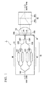
- FIG. 1 is a top view illustrating a configuration of an optical waveguide device according to the embodiment of the invention.
- the optical waveguide device 1 is a Modulator with Polarization Beam Combiner that outputs a beam that combined modulated and polarized beams, and includes: a modulator body 10 which modulates an input beam; 1/2-wave plates 30a and 30b (polarization beam rotating units) which rotate the polarizations of the beams output from the modulator body 10; a cylindrical lens 20 which collimates the beams output from the 1/2-wave plates 30a and 30b and changes the optical axises of the beams so as to be parallel to each other; and a element to combine polarization beam 40 (a polarization beam combining unit) which combines the differently polarized beams output from the cylindrical lens 20 so that the optical axes match each other.
- a modulator body 10 which modulates an input beam
- 1/2-wave plates 30a and 30b polarization beam rotating units
- cylindrical lens 20 which collimates the beams output from the
- the modulator body 10 is an optical waveguide element (LN optical modulator) in which optical waveguides and a modulation electrodes are mounted on a substrate formed of lithium niobate (LiNbO 3 : referred to as LN).
- the optical waveguides of the modulator body 10 has a nest structure in which both arms of a Mach-Zehnder waveguide MA are equipped with Mach-Zehnder waveguides MB and MC, both arms of the Mach-Zehnder waveguide MB are equipped with Mach-Zehnder waveguides 101 and 102, and both arms of the Mach-Zehnder waveguide MC are equipped with Mach-Zehnder waveguides 103 and 104.
- the input beam toward the modulator body 10 is introduced into an input waveguide 106 of the Mach-Zehnder waveguide MA, and is branched into the Mach-Zehnder waveguides MB and MC on the arms. Further, the beam which is input to the Mach-Zehnder waveguide MB is branched into the Mach-Zehnder waveguides 101 and 102, and the beam which is input to the Mach-Zehnder waveguide MC is branched into the Mach-Zehnder waveguides 103 and 104.
- the output beams from the Mach-Zehnder waveguides 101 and 102 are multiplexed by the Mach-Zehnder waveguide MB and are introduced into the arm 108 of the Mach-Zehnder waveguide MA.
- the output beams from the Mach-Zehnder waveguides 103 and 104 are multiplexed by the Mach-Zehnder waveguide MC and are introduced into the arm 109 of the Mach-Zehnder waveguide MA.
- the Mach-Zehnder waveguides 101 to 104 form an LN optical modulator together with the modulation electrodes (not shown) respectively installed therein.
- a driving signal of 10 Gb/s is applied from a driving circuit (not shown) to the modulation electrode of each of the LN optical modulators 101 to 104, and each of the LN optical modulators 101 to 104 outputs a modulated beam which is modulated into 10 Gb/s.
- DQPSK differential quadric-phase shift keying
- the beams which are introduced into the arms 108 and 109 of the Mach-Zehnder waveguide MA by DQPSK becomes a modulated beams of 20 Gb/s.
- the arm 108 of the Mach-Zehnder waveguide MA is formed so that the vicinity (an output waveguide 1081) of one end face M of the LN substrate (the modulator body 10) forms an angle ⁇ 1 with respect to the normal line of the end face M. Further, in the same way, the arm 109 of the Mach-Zehnder waveguide MA is formed so that the vicinity (an output waveguide 1091) of the end face M forms an angle ⁇ 2 with respect to the normal line of the end face M. In this way, since the output waveguides 1081 and 1091 are inclined with respect to the end face M, the reflected light from the end face M toward the output waveguides 1081 and 1091 may be reduced.
- angles ⁇ 1 and ⁇ 2 formed between the output waveguides 1081 and 1091 and the normal line of the end face M are in the range of, for example, 2° to 4°.
- the reflection loss (return loss) in the end faces M of the output waveguides 1081 and 1091 becomes 30 dB.
- the reflection loss becomes 55 dB.
- the 1/2-wave plate 30a rotates the polarization plane of the beam output from the output waveguide 1081 by 45°. Further, the 1/2-wave plate 30b rotates the polarization plane of the beam output from the output waveguide 1091 by 45° in a direction opposite to that of the beam output from the output waveguide 1081. Accordingly, the polarization planes of the beam output from the 1/2-wave plate 30a and the beam output from the 1/2-wave plate 30b are inclined with respect to each other by 90°.
- the refractive index of the lens, the curvature of the lens curved face, and the thickness of the lens are set so that the beams output from the 1/2-wave plates 30a and 30b are collimated and the optical axes of the beams passing through the cylindrical lens 20 are parallel to each other. Since the beams which are incident to the cylindrical lens 20 are disposed so as to be inclined with respect to the optical axis of the cylindrical lens 20, the beams output from the cylindrical lens 20 may be parallelized when the refractive index of the cylindrical lens 20, the curvature thereof, and the thickness thereof are adjusted in this way. Accordingly, there is no need to install a prism 60 which changes the optical path as in the existing configuration of FIG. 2 , which may realize a decrease in the number of components and a decrease in the size thereof.
- the element to combine polarization beam 40 two beams, which are incident to the different incident positions with polarization planes different by 90°, from the cylindrical lens 20, are output to the same optical path. Accordingly, a modulated beam of 40 Gb/s is obtained by combining modulated beams of 20 Gb/s of which the polarization planes are inclined with respect to each other by 90°.
- an element formed from rutile or calcite may be used as the element to combine polarization beam 40.
- a Savart plate which is formed by bonding two plates (the polarizing and separating plates 40a and 40b) having the same thickness and formed from rutile or the like so that the optical axes are perpendicular to each other.
- the Savart plate since the optical lengths of the beam from the arm 108 and the optical lengths of the beam from the arm 109 are equal, two beams may be polarized and combined with no difference in the optical path.
- the rotation angle of the polarization plane using the 1/2-wave plate 30a may be 90°
- the rotation angle of the polarization plane using the 1/2-wave plate 30b may be 0°.
- the 1/2-wave plate 30a and the 1/2-wave plate 30b may be installed between the cylindrical lens 20 and the element to combine polarization beam 40.
- a Selfoc lens may be used instead of the cylindrical lens 20.
- the beams output from the 1/2-wave plates 30a and 30b may be collimated and the optical axes of the beams passing through the Selfoc lens may be parallel to each other.
- the output waveguides 1081 and 1091 need to form the angles ⁇ 1 and ⁇ 2 with respect to the normal line of the end face M, but may not necessarily intersect each other inside the LN substrate (the modulator body 10) as shown in FIG. 1 ( FIG. 3 ).
- the Modulator with Polarization Beam Combiner has been exemplified, but the invention is not limited thereto. That is, the invention may be applied to the optical waveguide element other than the LN optical modulator.
Landscapes
- Physics & Mathematics (AREA)
- Engineering & Computer Science (AREA)
- Microelectronics & Electronic Packaging (AREA)
- General Physics & Mathematics (AREA)
- Optics & Photonics (AREA)
- Optical Integrated Circuits (AREA)
- Optical Modulation, Optical Deflection, Nonlinear Optics, Optical Demodulation, Optical Logic Elements (AREA)
Abstract
Description
- The present invention relates to an optical waveguide device.
Priority is claimed on Japanese Patent Application No.2009-225725, filed on September 30, 2009 - An existing optical waveguide device will be described by exemplifying a Modulator with Polarization Beam Combiner shown in
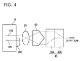
FIG. 4 . For example, modulated beams of 20 Gb/s are output fromoutput waveguides modulator body 11. The output beam from theoutput waveguide 108 is input to a element to combine polarization beam (a Savart plate) 40 through alens 50 and aprism 60. When the output beam from theoutput waveguide 109 passes through a 1/2-wave plate 30c, the polarization plane thereof rotates by 90°, and the beam is input to the element to combinepolarization beam 40 through thelens 50 and theprism 60. Two beams of which the polarization planes are inclined with respect to each other by 90° are output to the same optical path by the element to combinepolarization beam 40. In this way, a modulated beam of 40 Gb/s is obtained by combining the modulated beams of 20 Gb/s of which the polarization planes are inclined with respect to each other by 90°. -
- [PTL 1] Japanese Patent Application Laid-Open No.
2002-252420 - However, in the configuration of
FIG. 4 , since theoutput waveguides output waveguides
Further, in the configuration ofFIG. 4 , there is a need to use aprism 60 so that two beams incident to the element to combinepolarization beam 40 are changed into collimated parallel beams, which disturbs a decrease in the size of the optical waveguide device. - The invention is made in view of the above-described circumstances, and it is an object of the invention to provide a small optical waveguide device with little reflected light.
- The invention is made to solve the above-described problems. According to the invention, there is provided an optical waveguide device including: an optical waveguide element of which a first output waveguide is inclined with respect to an output end face and a second output waveguide is inclined with respect to both the first output waveguide and the output end face; and a lens that allows the beams respectively output from the first and second output waveguides to be parallel to each other.
- Further, according to the optical waveguide device of the invention, the first and second output waveguides preferably are symmetrical to each other with respect to the normal line of the output end face.
- Further, according to the optical waveguide device of the invention, the lens preferably allow the beams respectively output from the first and second output waveguides to be collimated beams parallel to each other.
- Further, according to the optical waveguide device of the invention, the optical waveguide device preferably includes: a polarization beam rotating unit that rotates the polarization of the beam output from the optical waveguide element or the lens; and a polarization beam combining unit that polarizes and combines the beams output from the polarization beam rotating unit.
- Further, according to the optical waveguide device of the invention, the optical waveguide element preferably include first and second optical modulating units, and is an optical modulator that outputs modulated beams using the first and second optical modulating units from the first and second output waveguides.
- According to the invention, it is possible to provide a small optical waveguide device with little reflected light.
-
-
FIG. 1 is a top view illustrating a configuration of an optical waveguide device according to an embodiment of the invention. -
FIG. 2 is a top view illustrating a configuration of the optical waveguide device according to an embodiment of the invention. -
FIG. 3 is a top view illustrating a configuration of the optical waveguide device according to an embodiment of the invention. -
FIG. 4 is a top view illustrating a configuration of an existing optical waveguide device. - Hereinafter, an embodiment of the invention will be described in detail by referring to the drawings.
FIG. 1 is a top view illustrating a configuration of an optical waveguide device according to the embodiment of the invention. Theoptical waveguide device 1 is a Modulator with Polarization Beam Combiner that outputs a beam that combined modulated and polarized beams, and includes: amodulator body 10 which modulates an input beam; 1/2-wave plates modulator body 10; acylindrical lens 20 which collimates the beams output from the 1/2-wave plates cylindrical lens 20 so that the optical axes match each other. - The
modulator body 10 is an optical waveguide element (LN optical modulator) in which optical waveguides and a modulation electrodes are mounted on a substrate formed of lithium niobate (LiNbO3: referred to as LN).
The optical waveguides of themodulator body 10 has a nest structure in which both arms of a Mach-Zehnder waveguide MA are equipped with Mach-Zehnder waveguides MB and MC, both arms of the Mach-Zehnder waveguide MB are equipped with Mach-Zehnderwaveguides waveguides modulator body 10 is introduced into aninput waveguide 106 of the Mach-Zehnder waveguide MA, and is branched into the Mach-Zehnder waveguides MB and MC on the arms. Further, the beam which is input to the Mach-Zehnder waveguide MB is branched into the Mach-Zehnderwaveguides waveguides waveguides arm 108 of the Mach-Zehnder waveguide MA. The output beams from the Mach-Zehnderwaveguides arm 109 of the Mach-Zehnder waveguide MA. - The Mach-Zehnder
waveguides 101 to 104 (the optical modulating units) form an LN optical modulator together with the modulation electrodes (not shown) respectively installed therein. For example, a driving signal of 10 Gb/s is applied from a driving circuit (not shown) to the modulation electrode of each of the LNoptical modulators 101 to 104, and each of the LNoptical modulators 101 to 104 outputs a modulated beam which is modulated into 10 Gb/s. As the modulation type of the LNoptical modulators optical modulators arms - The
arm 108 of the Mach-Zehnder waveguide MA is formed so that the vicinity (an output waveguide 1081) of one end face M of the LN substrate (the modulator body 10) forms an angle θ1 with respect to the normal line of the end face M. Further, in the same way, thearm 109 of the Mach-Zehnder waveguide MA is formed so that the vicinity (an output waveguide 1091) of the end face M forms an angle θ2 with respect to the normal line of the end face M. In this way, since theoutput waveguides output waveguides - Here, it is desirable to set the angles θ1 and θ2 formed between the
output waveguides output waveguides output waveguides output waveguides - The 1/2-
wave plate 30a rotates the polarization plane of the beam output from theoutput waveguide 1081 by 45°. Further, the 1/2-wave plate 30b rotates the polarization plane of the beam output from theoutput waveguide 1091 by 45° in a direction opposite to that of the beam output from theoutput waveguide 1081. Accordingly, the polarization planes of the beam output from the 1/2-wave plate 30a and the beam output from the 1/2-wave plate 30b are inclined with respect to each other by 90°. - With regard to the
cylindrical lens 20, the refractive index of the lens, the curvature of the lens curved face, and the thickness of the lens are set so that the beams output from the 1/2-wave plates cylindrical lens 20 are parallel to each other. Since the beams which are incident to thecylindrical lens 20 are disposed so as to be inclined with respect to the optical axis of thecylindrical lens 20, the beams output from thecylindrical lens 20 may be parallelized when the refractive index of thecylindrical lens 20, the curvature thereof, and the thickness thereof are adjusted in this way. Accordingly, there is no need to install aprism 60 which changes the optical path as in the existing configuration ofFIG. 2 , which may realize a decrease in the number of components and a decrease in the size thereof. - In the element to combine
polarization beam 40, two beams, which are incident to the different incident positions with polarization planes different by 90°, from thecylindrical lens 20, are output to the same optical path. Accordingly, a modulated beam of 40 Gb/s is obtained by combining modulated beams of 20 Gb/s of which the polarization planes are inclined with respect to each other by 90°. As the element to combinepolarization beam 40, for example, an element formed from rutile or calcite may be used. However, particularly, it is desirable to use a Savart plate which is formed by bonding two plates (the polarizing and separatingplates arm 108 and the optical lengths of the beam from thearm 109 are equal, two beams may be polarized and combined with no difference in the optical path. - While the embodiment of the invention has been described by referring to the drawings, the detailed configuration is not limited to the above-described configuration, and the design and the like may be modified into various forms within the scope of the concept of the invention. For example, the rotation angle of the polarization plane using the 1/2-
wave plate 30a may be 90°, and the rotation angle of the polarization plane using the 1/2-wave plate 30b may be 0°. Further, as shown inFIG. 2 , the 1/2-wave plate 30a and the 1/2-wave plate 30b may be installed between thecylindrical lens 20 and the element to combinepolarization beam 40.
Further, instead of thecylindrical lens 20, a Selfoc lens may be used. When the refractive index distribution and the thickness (the length in the optical axis direction) of the Selfoc lens are appropriately set, the beams output from the 1/2-wave plates
Further, as described above, theoutput waveguides FIG. 1 (FIG. 3 ).
Further, in the above-described embodiment, the Modulator with Polarization Beam Combiner has been exemplified, but the invention is not limited thereto. That is, the invention may be applied to the optical waveguide element other than the LN optical modulator. - According to the invention, it is possible to provide a small optical waveguide device with little reflected light.
-
- 1:
- OPTICAL WAVEGUIDE DEVICE
- 10:
- MODULATOR BODY
- MA, MB, MC, 101 TO 104:
- MACH-ZEHNDER WAVEGUIDE
- 106:
- INPUT WAVEGUIDE
- 108, 109:
- ARM OF MACH-ZEHNDER WAVEGUIDE
- 1081, 1091:
- OUTPUT WAVEGUIDE
- 20:
- CYLINDRICAL LENS
- 30a, 30b:
- 1/2-WAVE PLATE
- 40:
- ELEMENT TO COMBINE POLARIZATION BEAM
- 40a, 40b:
- POLARIZING AND SEPARATING PLATE
Claims (5)
- An optical waveguide device comprising:an optical waveguide element of which a first output waveguide is inclined with respect to an output end face and a second output waveguide is inclined with respect to both the first output waveguide and the output end face; anda lens that allows beams respectively output from the first and second output waveguides to be parallel to each other.
- The optical waveguide device according to claim 1, wherein the first and second output waveguides are symmetrical to each other with respect to the normal line of the output end face.
- The optical waveguide device according to claim 1 or 2,
wherein the lens allows the beams respectively output from the first and second output waveguides to be collimated beams parallel to each other. - The optical waveguide device according to claim 1 or 2, further comprising:a polarization beam rotating unit that rotates the polarization of the beam output from the optical waveguide element or the lens; anda polarization beam combining unit that polarizes and combines the beams output from the polarization beam rotating unit.
- The optical waveguide device according to claim 1 or 2,
wherein the optical waveguide element includes first and second optical modulating units, and is an optical modulator that outputs modulated beams using the first and second optical modulating units from the first and second output waveguides.
Applications Claiming Priority (2)
| Application Number | Priority Date | Filing Date | Title |
|---|---|---|---|
| JP2009225725A JP4937325B2 (en) | 2009-09-30 | 2009-09-30 | Optical waveguide device |
| PCT/JP2010/066580 WO2011040339A1 (en) | 2009-09-30 | 2010-09-24 | Optical waveguide device |
Publications (3)
| Publication Number | Publication Date |
|---|---|
| EP2485076A1 true EP2485076A1 (en) | 2012-08-08 |
| EP2485076A4 EP2485076A4 (en) | 2017-12-27 |
| EP2485076B1 EP2485076B1 (en) | 2020-06-17 |
Family
ID=43826159
Family Applications (1)
| Application Number | Title | Priority Date | Filing Date |
|---|---|---|---|
| EP10820456.1A Active EP2485076B1 (en) | 2009-09-30 | 2010-09-24 | Optical waveguide device |
Country Status (5)
| Country | Link |
|---|---|
| US (1) | US9081139B2 (en) |
| EP (1) | EP2485076B1 (en) |
| JP (1) | JP4937325B2 (en) |
| CN (1) | CN102576124B (en) |
| WO (1) | WO2011040339A1 (en) |
Cited By (1)
| Publication number | Priority date | Publication date | Assignee | Title |
|---|---|---|---|---|
| EP3270214A4 (en) * | 2016-03-16 | 2018-11-21 | Sumitomo Osaka Cement Co., Ltd. | Optical modulation device |
Families Citing this family (13)
| Publication number | Priority date | Publication date | Assignee | Title |
|---|---|---|---|---|
| JP2013029653A (en) * | 2011-07-28 | 2013-02-07 | Sumitomo Osaka Cement Co Ltd | Optical device, polarized wave synthesizer and method for manufacturing optical device |
| EP2778771B1 (en) * | 2011-09-30 | 2017-12-13 | Sumitomo Osaka Cement Co., Ltd. | Carrier-suppressed light-generating device |
| JP5834994B2 (en) * | 2012-02-21 | 2015-12-24 | 住友電気工業株式会社 | DP-QPSK optical modulator |
| JP2013246325A (en) * | 2012-05-25 | 2013-12-09 | Sumitomo Osaka Cement Co Ltd | Optical modulator |
| JP2014059475A (en) * | 2012-09-18 | 2014-04-03 | Sumitomo Osaka Cement Co Ltd | Optical modulator |
| WO2014051096A1 (en) * | 2012-09-28 | 2014-04-03 | 住友大阪セメント株式会社 | Optical modulator and optical modulation method |
| JP5573985B1 (en) * | 2013-01-31 | 2014-08-20 | 住友大阪セメント株式会社 | Light modulator |
| CN103091869B (en) * | 2013-02-05 | 2018-08-10 | 中国科学院半导体研究所 | Integrated coherent light communication electrooptical modulator structure |
| JP6460411B2 (en) * | 2013-08-01 | 2019-01-30 | シーシーエス株式会社 | Light source device |
| JP6361176B2 (en) * | 2014-03-07 | 2018-07-25 | 富士通オプティカルコンポーネンツ株式会社 | Optical transmitter |
| WO2017170194A1 (en) * | 2016-03-31 | 2017-10-05 | 住友大阪セメント株式会社 | Optical modulation device |
| JP6784144B2 (en) * | 2016-10-28 | 2020-11-11 | 富士通オプティカルコンポーネンツ株式会社 | Optical module |
| JP2020086082A (en) * | 2018-11-22 | 2020-06-04 | 日本電信電話株式会社 | Optical connection structure |
Family Cites Families (23)
| Publication number | Priority date | Publication date | Assignee | Title |
|---|---|---|---|---|
| US4343535A (en) * | 1979-12-14 | 1982-08-10 | Hughes Aircraft Company | Liquid crystal light valve |
| NL8101826A (en) * | 1981-04-14 | 1982-11-01 | Philips Nv | OPTICAL MULTIPLEX DEVICE. |
| JP3737566B2 (en) * | 1996-06-20 | 2006-01-18 | 富士通株式会社 | Optical device |
| JPH11258454A (en) * | 1998-03-10 | 1999-09-24 | Fujitsu Ltd | Multi-axis optical coupling device |
| JP2000098156A (en) * | 1998-09-25 | 2000-04-07 | Oki Electric Ind Co Ltd | Optical waveguide device, end structure of optical fiber array, and method of manufacturing the same |
| US6167174A (en) * | 1998-10-27 | 2000-12-26 | Adc Telecommunications, Inc. | Multiple port, fiber optic isolator |
| US6607313B1 (en) * | 1999-06-23 | 2003-08-19 | Jds Fitel Inc. | Micro-optic delay element for use in a polarization multiplexed system |
| US7200289B2 (en) * | 2000-03-15 | 2007-04-03 | Sumitomo Osaka Cement Co., Ltd. | Optical waveguide modulator with output light monitor |
| CN1204662C (en) * | 2000-12-15 | 2005-06-01 | 古河电气工业株式会社 | Semiconductor laser module and its making method and light amplifier |
| JP3794561B2 (en) * | 2000-12-15 | 2006-07-05 | 古河電気工業株式会社 | Semiconductor laser module and optical amplifier |
| JP2002252420A (en) | 2000-12-15 | 2002-09-06 | Furukawa Electric Co Ltd:The | Semiconductor laser device, semiconductor laser module, method of manufacturing the same, and optical fiber amplifier |
| KR100896227B1 (en) * | 2001-03-30 | 2009-05-08 | 소니 가부시끼 가이샤 | Optical pickup and optical disc drive device |
| JP2004006439A (en) * | 2001-07-02 | 2004-01-08 | Furukawa Electric Co Ltd:The | Semiconductor laser module and method of manufacturing the same |
| US6741764B2 (en) * | 2001-11-13 | 2004-05-25 | Adc Telecommunications, Inc. | Polarization beam separator and combiner |
| JP2004317626A (en) * | 2003-04-14 | 2004-11-11 | Fujikura Ltd | Mount and optical transmission module |
| JP3902619B2 (en) * | 2003-10-30 | 2007-04-11 | Tdk株式会社 | Optical multiplexer / demultiplexer and manufacturing method thereof |
| JP2006047956A (en) * | 2004-06-29 | 2006-02-16 | Anritsu Corp | Waveguide type optical device |
| US7277216B2 (en) * | 2004-11-26 | 2007-10-02 | Alces Technology | Differential interferometric light modulator and image display system |
| JP2007304525A (en) * | 2006-05-15 | 2007-11-22 | Ricoh Co Ltd | Image input apparatus, electronic apparatus, and image input method |
| JP4894579B2 (en) * | 2007-03-20 | 2012-03-14 | ソニー株式会社 | Lens housing and optical module |
| JP2009225725A (en) | 2008-03-24 | 2009-10-08 | Kanetsu Giken Kk | Emergency ventilator for livestock barn |
| CN101345585B (en) * | 2008-08-20 | 2010-12-22 | 武汉光迅科技股份有限公司 | Optical Differential Quadrature Phase Shift Keying Modulator with Nested Mach-Zehnder Waveguide Structure |
| JP5201508B2 (en) * | 2008-09-18 | 2013-06-05 | 独立行政法人産業技術総合研究所 | Waveguide-type wavelength domain optical switch |
-
2009
- 2009-09-30 JP JP2009225725A patent/JP4937325B2/en not_active Expired - Fee Related
-
2010
- 2010-09-24 WO PCT/JP2010/066580 patent/WO2011040339A1/en not_active Ceased
- 2010-09-24 CN CN201080043253.7A patent/CN102576124B/en not_active Expired - Fee Related
- 2010-09-24 EP EP10820456.1A patent/EP2485076B1/en active Active
- 2010-09-24 US US13/498,589 patent/US9081139B2/en active Active
Non-Patent Citations (1)
| Title |
|---|
| See references of WO2011040339A1 * |
Cited By (1)
| Publication number | Priority date | Publication date | Assignee | Title |
|---|---|---|---|---|
| EP3270214A4 (en) * | 2016-03-16 | 2018-11-21 | Sumitomo Osaka Cement Co., Ltd. | Optical modulation device |
Also Published As
| Publication number | Publication date |
|---|---|
| WO2011040339A1 (en) | 2011-04-07 |
| EP2485076B1 (en) | 2020-06-17 |
| EP2485076A4 (en) | 2017-12-27 |
| CN102576124B (en) | 2015-07-08 |
| JP4937325B2 (en) | 2012-05-23 |
| US20120183252A1 (en) | 2012-07-19 |
| US9081139B2 (en) | 2015-07-14 |
| CN102576124A (en) | 2012-07-11 |
| JP2011075739A (en) | 2011-04-14 |
Similar Documents
| Publication | Publication Date | Title |
|---|---|---|
| EP2485076B1 (en) | Optical waveguide device | |
| US20110255147A1 (en) | Optical modulator | |
| CN104981727B (en) | light modulator | |
| US8909006B2 (en) | Optical waveguide device | |
| US8437068B2 (en) | Optical modulator | |
| JP5621861B2 (en) | Optical device | |
| US9448457B2 (en) | Optical modulator | |
| JP5673283B2 (en) | Polarization synthesizer | |
| JP6233366B2 (en) | Light modulator | |
| JP5659631B2 (en) | Polarization controller | |
| US10268099B2 (en) | Optical modulator and optical module | |
| US20190113683A1 (en) | Optical modulation device | |
| JP6413807B2 (en) | Light modulator | |
| JP2012211971A (en) | Polarized wave synthesizer | |
| US20190004249A1 (en) | Optical modulation device | |
| JP2021189227A (en) | Optical modulator | |
| WO2019188093A1 (en) | Optical modulation device |
Legal Events
| Date | Code | Title | Description |
|---|---|---|---|
| PUAI | Public reference made under article 153(3) epc to a published international application that has entered the european phase |
Free format text: ORIGINAL CODE: 0009012 |
|
| 17P | Request for examination filed |
Effective date: 20120417 |
|
| AK | Designated contracting states |
Kind code of ref document: A1 Designated state(s): AL AT BE BG CH CY CZ DE DK EE ES FI FR GB GR HR HU IE IS IT LI LT LU LV MC MK MT NL NO PL PT RO SE SI SK SM TR |
|
| DAX | Request for extension of the european patent (deleted) | ||
| RA4 | Supplementary search report drawn up and despatched (corrected) |
Effective date: 20171124 |
|
| RIC1 | Information provided on ipc code assigned before grant |
Ipc: G02B 6/125 20060101ALI20171120BHEP Ipc: G02B 6/122 20060101AFI20171120BHEP Ipc: G02B 6/27 20060101ALI20171120BHEP Ipc: G02B 6/12 20060101ALI20171120BHEP Ipc: G02F 1/035 20060101ALI20171120BHEP |
|
| STAA | Information on the status of an ep patent application or granted ep patent |
Free format text: STATUS: EXAMINATION IS IN PROGRESS |
|
| 17Q | First examination report despatched |
Effective date: 20190405 |
|
| GRAP | Despatch of communication of intention to grant a patent |
Free format text: ORIGINAL CODE: EPIDOSNIGR1 |
|
| STAA | Information on the status of an ep patent application or granted ep patent |
Free format text: STATUS: GRANT OF PATENT IS INTENDED |
|
| INTG | Intention to grant announced |
Effective date: 20200110 |
|
| GRAS | Grant fee paid |
Free format text: ORIGINAL CODE: EPIDOSNIGR3 |
|
| GRAA | (expected) grant |
Free format text: ORIGINAL CODE: 0009210 |
|
| STAA | Information on the status of an ep patent application or granted ep patent |
Free format text: STATUS: THE PATENT HAS BEEN GRANTED |
|
| RAP1 | Party data changed (applicant data changed or rights of an application transferred) |
Owner name: SUMITOMO OSAKA CEMENT CO., LTD. |
|
| AK | Designated contracting states |
Kind code of ref document: B1 Designated state(s): AL AT BE BG CH CY CZ DE DK EE ES FI FR GB GR HR HU IE IS IT LI LT LU LV MC MK MT NL NO PL PT RO SE SI SK SM TR |
|
| REG | Reference to a national code |
Ref country code: GB Ref legal event code: FG4D |
|
| REG | Reference to a national code |
Ref country code: CH Ref legal event code: EP |
|
| REG | Reference to a national code |
Ref country code: IE Ref legal event code: FG4D |
|
| REG | Reference to a national code |
Ref country code: DE Ref legal event code: R096 Ref document number: 602010064661 Country of ref document: DE |
|
| REG | Reference to a national code |
Ref country code: AT Ref legal event code: REF Ref document number: 1282025 Country of ref document: AT Kind code of ref document: T Effective date: 20200715 |
|
| PG25 | Lapsed in a contracting state [announced via postgrant information from national office to epo] |
Ref country code: FI Free format text: LAPSE BECAUSE OF FAILURE TO SUBMIT A TRANSLATION OF THE DESCRIPTION OR TO PAY THE FEE WITHIN THE PRESCRIBED TIME-LIMIT Effective date: 20200617 Ref country code: NO Free format text: LAPSE BECAUSE OF FAILURE TO SUBMIT A TRANSLATION OF THE DESCRIPTION OR TO PAY THE FEE WITHIN THE PRESCRIBED TIME-LIMIT Effective date: 20200917 Ref country code: GR Free format text: LAPSE BECAUSE OF FAILURE TO SUBMIT A TRANSLATION OF THE DESCRIPTION OR TO PAY THE FEE WITHIN THE PRESCRIBED TIME-LIMIT Effective date: 20200918 Ref country code: SE Free format text: LAPSE BECAUSE OF FAILURE TO SUBMIT A TRANSLATION OF THE DESCRIPTION OR TO PAY THE FEE WITHIN THE PRESCRIBED TIME-LIMIT Effective date: 20200617 Ref country code: LT Free format text: LAPSE BECAUSE OF FAILURE TO SUBMIT A TRANSLATION OF THE DESCRIPTION OR TO PAY THE FEE WITHIN THE PRESCRIBED TIME-LIMIT Effective date: 20200617 |
|
| REG | Reference to a national code |
Ref country code: LT Ref legal event code: MG4D |
|
| REG | Reference to a national code |
Ref country code: NL Ref legal event code: MP Effective date: 20200617 |
|
| PG25 | Lapsed in a contracting state [announced via postgrant information from national office to epo] |
Ref country code: BG Free format text: LAPSE BECAUSE OF FAILURE TO SUBMIT A TRANSLATION OF THE DESCRIPTION OR TO PAY THE FEE WITHIN THE PRESCRIBED TIME-LIMIT Effective date: 20200917 Ref country code: LV Free format text: LAPSE BECAUSE OF FAILURE TO SUBMIT A TRANSLATION OF THE DESCRIPTION OR TO PAY THE FEE WITHIN THE PRESCRIBED TIME-LIMIT Effective date: 20200617 Ref country code: HR Free format text: LAPSE BECAUSE OF FAILURE TO SUBMIT A TRANSLATION OF THE DESCRIPTION OR TO PAY THE FEE WITHIN THE PRESCRIBED TIME-LIMIT Effective date: 20200617 |
|
| REG | Reference to a national code |
Ref country code: AT Ref legal event code: MK05 Ref document number: 1282025 Country of ref document: AT Kind code of ref document: T Effective date: 20200617 |
|
| PG25 | Lapsed in a contracting state [announced via postgrant information from national office to epo] |
Ref country code: AL Free format text: LAPSE BECAUSE OF FAILURE TO SUBMIT A TRANSLATION OF THE DESCRIPTION OR TO PAY THE FEE WITHIN THE PRESCRIBED TIME-LIMIT Effective date: 20200617 Ref country code: NL Free format text: LAPSE BECAUSE OF FAILURE TO SUBMIT A TRANSLATION OF THE DESCRIPTION OR TO PAY THE FEE WITHIN THE PRESCRIBED TIME-LIMIT Effective date: 20200617 |
|
| PG25 | Lapsed in a contracting state [announced via postgrant information from national office to epo] |
Ref country code: EE Free format text: LAPSE BECAUSE OF FAILURE TO SUBMIT A TRANSLATION OF THE DESCRIPTION OR TO PAY THE FEE WITHIN THE PRESCRIBED TIME-LIMIT Effective date: 20200617 Ref country code: AT Free format text: LAPSE BECAUSE OF FAILURE TO SUBMIT A TRANSLATION OF THE DESCRIPTION OR TO PAY THE FEE WITHIN THE PRESCRIBED TIME-LIMIT Effective date: 20200617 Ref country code: SM Free format text: LAPSE BECAUSE OF FAILURE TO SUBMIT A TRANSLATION OF THE DESCRIPTION OR TO PAY THE FEE WITHIN THE PRESCRIBED TIME-LIMIT Effective date: 20200617 Ref country code: PT Free format text: LAPSE BECAUSE OF FAILURE TO SUBMIT A TRANSLATION OF THE DESCRIPTION OR TO PAY THE FEE WITHIN THE PRESCRIBED TIME-LIMIT Effective date: 20201019 Ref country code: IT Free format text: LAPSE BECAUSE OF FAILURE TO SUBMIT A TRANSLATION OF THE DESCRIPTION OR TO PAY THE FEE WITHIN THE PRESCRIBED TIME-LIMIT Effective date: 20200617 Ref country code: ES Free format text: LAPSE BECAUSE OF FAILURE TO SUBMIT A TRANSLATION OF THE DESCRIPTION OR TO PAY THE FEE WITHIN THE PRESCRIBED TIME-LIMIT Effective date: 20200617 Ref country code: CZ Free format text: LAPSE BECAUSE OF FAILURE TO SUBMIT A TRANSLATION OF THE DESCRIPTION OR TO PAY THE FEE WITHIN THE PRESCRIBED TIME-LIMIT Effective date: 20200617 Ref country code: RO Free format text: LAPSE BECAUSE OF FAILURE TO SUBMIT A TRANSLATION OF THE DESCRIPTION OR TO PAY THE FEE WITHIN THE PRESCRIBED TIME-LIMIT Effective date: 20200617 |
|
| PG25 | Lapsed in a contracting state [announced via postgrant information from national office to epo] |
Ref country code: PL Free format text: LAPSE BECAUSE OF FAILURE TO SUBMIT A TRANSLATION OF THE DESCRIPTION OR TO PAY THE FEE WITHIN THE PRESCRIBED TIME-LIMIT Effective date: 20200617 Ref country code: SK Free format text: LAPSE BECAUSE OF FAILURE TO SUBMIT A TRANSLATION OF THE DESCRIPTION OR TO PAY THE FEE WITHIN THE PRESCRIBED TIME-LIMIT Effective date: 20200617 Ref country code: IS Free format text: LAPSE BECAUSE OF FAILURE TO SUBMIT A TRANSLATION OF THE DESCRIPTION OR TO PAY THE FEE WITHIN THE PRESCRIBED TIME-LIMIT Effective date: 20201017 |
|
| REG | Reference to a national code |
Ref country code: DE Ref legal event code: R097 Ref document number: 602010064661 Country of ref document: DE |
|
| PLBE | No opposition filed within time limit |
Free format text: ORIGINAL CODE: 0009261 |
|
| STAA | Information on the status of an ep patent application or granted ep patent |
Free format text: STATUS: NO OPPOSITION FILED WITHIN TIME LIMIT |
|
| PG25 | Lapsed in a contracting state [announced via postgrant information from national office to epo] |
Ref country code: MC Free format text: LAPSE BECAUSE OF FAILURE TO SUBMIT A TRANSLATION OF THE DESCRIPTION OR TO PAY THE FEE WITHIN THE PRESCRIBED TIME-LIMIT Effective date: 20200617 Ref country code: DK Free format text: LAPSE BECAUSE OF FAILURE TO SUBMIT A TRANSLATION OF THE DESCRIPTION OR TO PAY THE FEE WITHIN THE PRESCRIBED TIME-LIMIT Effective date: 20200617 |
|
| REG | Reference to a national code |
Ref country code: CH Ref legal event code: PL |
|
| 26N | No opposition filed |
Effective date: 20210318 |
|
| GBPC | Gb: european patent ceased through non-payment of renewal fee |
Effective date: 20200924 |
|
| PG25 | Lapsed in a contracting state [announced via postgrant information from national office to epo] |
Ref country code: SI Free format text: LAPSE BECAUSE OF FAILURE TO SUBMIT A TRANSLATION OF THE DESCRIPTION OR TO PAY THE FEE WITHIN THE PRESCRIBED TIME-LIMIT Effective date: 20200617 |
|
| REG | Reference to a national code |
Ref country code: BE Ref legal event code: MM Effective date: 20200930 |
|
| PG25 | Lapsed in a contracting state [announced via postgrant information from national office to epo] |
Ref country code: LU Free format text: LAPSE BECAUSE OF NON-PAYMENT OF DUE FEES Effective date: 20200924 |
|
| PG25 | Lapsed in a contracting state [announced via postgrant information from national office to epo] |
Ref country code: FR Free format text: LAPSE BECAUSE OF NON-PAYMENT OF DUE FEES Effective date: 20200930 |
|
| PG25 | Lapsed in a contracting state [announced via postgrant information from national office to epo] |
Ref country code: CH Free format text: LAPSE BECAUSE OF NON-PAYMENT OF DUE FEES Effective date: 20200930 Ref country code: BE Free format text: LAPSE BECAUSE OF NON-PAYMENT OF DUE FEES Effective date: 20200930 Ref country code: GB Free format text: LAPSE BECAUSE OF NON-PAYMENT OF DUE FEES Effective date: 20200924 Ref country code: IE Free format text: LAPSE BECAUSE OF NON-PAYMENT OF DUE FEES Effective date: 20200924 Ref country code: LI Free format text: LAPSE BECAUSE OF NON-PAYMENT OF DUE FEES Effective date: 20200930 |
|
| PG25 | Lapsed in a contracting state [announced via postgrant information from national office to epo] |
Ref country code: TR Free format text: LAPSE BECAUSE OF FAILURE TO SUBMIT A TRANSLATION OF THE DESCRIPTION OR TO PAY THE FEE WITHIN THE PRESCRIBED TIME-LIMIT Effective date: 20200617 Ref country code: MT Free format text: LAPSE BECAUSE OF FAILURE TO SUBMIT A TRANSLATION OF THE DESCRIPTION OR TO PAY THE FEE WITHIN THE PRESCRIBED TIME-LIMIT Effective date: 20200617 Ref country code: CY Free format text: LAPSE BECAUSE OF FAILURE TO SUBMIT A TRANSLATION OF THE DESCRIPTION OR TO PAY THE FEE WITHIN THE PRESCRIBED TIME-LIMIT Effective date: 20200617 |
|
| PG25 | Lapsed in a contracting state [announced via postgrant information from national office to epo] |
Ref country code: MK Free format text: LAPSE BECAUSE OF FAILURE TO SUBMIT A TRANSLATION OF THE DESCRIPTION OR TO PAY THE FEE WITHIN THE PRESCRIBED TIME-LIMIT Effective date: 20200617 |
|
| P01 | Opt-out of the competence of the unified patent court (upc) registered |
Effective date: 20230527 |
|
| PGFP | Annual fee paid to national office [announced via postgrant information from national office to epo] |
Ref country code: DE Payment date: 20230920 Year of fee payment: 14 |
|
| REG | Reference to a national code |
Ref country code: DE Ref legal event code: R119 Ref document number: 602010064661 Country of ref document: DE |
|
| PG25 | Lapsed in a contracting state [announced via postgrant information from national office to epo] |
Ref country code: DE Free format text: LAPSE BECAUSE OF NON-PAYMENT OF DUE FEES Effective date: 20250401 |