EP2484817A1 - Method for preserving a gallium nitride substrate, preserved gallium nitride substrate, semiconductor device, and manufacturing method therefor - Google Patents
Method for preserving a gallium nitride substrate, preserved gallium nitride substrate, semiconductor device, and manufacturing method therefor Download PDFInfo
- Publication number
- EP2484817A1 EP2484817A1 EP10820226A EP10820226A EP2484817A1 EP 2484817 A1 EP2484817 A1 EP 2484817A1 EP 10820226 A EP10820226 A EP 10820226A EP 10820226 A EP10820226 A EP 10820226A EP 2484817 A1 EP2484817 A1 EP 2484817A1
- Authority
- EP
- European Patent Office
- Prior art keywords
- gan
- plane
- gan substrate
- less
- principal face
- Prior art date
- Legal status (The legal status is an assumption and is not a legal conclusion. Google has not performed a legal analysis and makes no representation as to the accuracy of the status listed.)
- Granted
Links
Images




Classifications
-
- C—CHEMISTRY; METALLURGY
- C30—CRYSTAL GROWTH
- C30B—SINGLE-CRYSTAL GROWTH; UNIDIRECTIONAL SOLIDIFICATION OF EUTECTIC MATERIAL OR UNIDIRECTIONAL DEMIXING OF EUTECTOID MATERIAL; REFINING BY ZONE-MELTING OF MATERIAL; PRODUCTION OF A HOMOGENEOUS POLYCRYSTALLINE MATERIAL WITH DEFINED STRUCTURE; SINGLE CRYSTALS OR HOMOGENEOUS POLYCRYSTALLINE MATERIAL WITH DEFINED STRUCTURE; AFTER-TREATMENT OF SINGLE CRYSTALS OR A HOMOGENEOUS POLYCRYSTALLINE MATERIAL WITH DEFINED STRUCTURE; APPARATUS THEREFOR
- C30B29/00—Single crystals or homogeneous polycrystalline material with defined structure characterised by the material or by their shape
- C30B29/10—Inorganic compounds or compositions
- C30B29/40—AIIIBV compounds wherein A is B, Al, Ga, In or Tl and B is N, P, As, Sb or Bi
- C30B29/403—AIII-nitrides
- C30B29/406—Gallium nitride
-
- C—CHEMISTRY; METALLURGY
- C30—CRYSTAL GROWTH
- C30B—SINGLE-CRYSTAL GROWTH; UNIDIRECTIONAL SOLIDIFICATION OF EUTECTIC MATERIAL OR UNIDIRECTIONAL DEMIXING OF EUTECTOID MATERIAL; REFINING BY ZONE-MELTING OF MATERIAL; PRODUCTION OF A HOMOGENEOUS POLYCRYSTALLINE MATERIAL WITH DEFINED STRUCTURE; SINGLE CRYSTALS OR HOMOGENEOUS POLYCRYSTALLINE MATERIAL WITH DEFINED STRUCTURE; AFTER-TREATMENT OF SINGLE CRYSTALS OR A HOMOGENEOUS POLYCRYSTALLINE MATERIAL WITH DEFINED STRUCTURE; APPARATUS THEREFOR
- C30B33/00—After-treatment of single crystals or homogeneous polycrystalline material with defined structure
-
- H—ELECTRICITY
- H10—SEMICONDUCTOR DEVICES; ELECTRIC SOLID-STATE DEVICES NOT OTHERWISE PROVIDED FOR
- H10H—INORGANIC LIGHT-EMITTING SEMICONDUCTOR DEVICES HAVING POTENTIAL BARRIERS
- H10H20/00—Individual inorganic light-emitting semiconductor devices having potential barriers, e.g. light-emitting diodes [LED]
- H10H20/01—Manufacture or treatment
- H10H20/011—Manufacture or treatment of bodies, e.g. forming semiconductor layers
- H10H20/013—Manufacture or treatment of bodies, e.g. forming semiconductor layers having light-emitting regions comprising only Group III-V materials
- H10H20/0137—Manufacture or treatment of bodies, e.g. forming semiconductor layers having light-emitting regions comprising only Group III-V materials the light-emitting regions comprising nitride materials
-
- H—ELECTRICITY
- H10—SEMICONDUCTOR DEVICES; ELECTRIC SOLID-STATE DEVICES NOT OTHERWISE PROVIDED FOR
- H10H—INORGANIC LIGHT-EMITTING SEMICONDUCTOR DEVICES HAVING POTENTIAL BARRIERS
- H10H20/00—Individual inorganic light-emitting semiconductor devices having potential barriers, e.g. light-emitting diodes [LED]
- H10H20/80—Constructional details
- H10H20/81—Bodies
- H10H20/817—Bodies characterised by the crystal structures or orientations, e.g. polycrystalline, amorphous or porous
-
- H—ELECTRICITY
- H10—SEMICONDUCTOR DEVICES; ELECTRIC SOLID-STATE DEVICES NOT OTHERWISE PROVIDED FOR
- H10H—INORGANIC LIGHT-EMITTING SEMICONDUCTOR DEVICES HAVING POTENTIAL BARRIERS
- H10H20/00—Individual inorganic light-emitting semiconductor devices having potential barriers, e.g. light-emitting diodes [LED]
- H10H20/80—Constructional details
- H10H20/84—Coatings, e.g. passivation layers or antireflective coatings
- H10H20/841—Reflective coatings, e.g. dielectric Bragg reflectors
-
- H—ELECTRICITY
- H10—SEMICONDUCTOR DEVICES; ELECTRIC SOLID-STATE DEVICES NOT OTHERWISE PROVIDED FOR
- H10P—GENERIC PROCESSES OR APPARATUS FOR THE MANUFACTURE OR TREATMENT OF DEVICES COVERED BY CLASS H10
- H10P14/00—Formation of materials, e.g. in the shape of layers or pillars
- H10P14/20—Formation of materials, e.g. in the shape of layers or pillars of semiconductor materials
- H10P14/29—Formation of materials, e.g. in the shape of layers or pillars of semiconductor materials characterised by the substrates
- H10P14/2901—Materials
- H10P14/2907—Materials being Group IIIA-VA materials
- H10P14/2908—Nitrides
-
- H—ELECTRICITY
- H10—SEMICONDUCTOR DEVICES; ELECTRIC SOLID-STATE DEVICES NOT OTHERWISE PROVIDED FOR
- H10P—GENERIC PROCESSES OR APPARATUS FOR THE MANUFACTURE OR TREATMENT OF DEVICES COVERED BY CLASS H10
- H10P14/00—Formation of materials, e.g. in the shape of layers or pillars
- H10P14/20—Formation of materials, e.g. in the shape of layers or pillars of semiconductor materials
- H10P14/29—Formation of materials, e.g. in the shape of layers or pillars of semiconductor materials characterised by the substrates
- H10P14/2926—Crystal orientations
-
- H—ELECTRICITY
- H10—SEMICONDUCTOR DEVICES; ELECTRIC SOLID-STATE DEVICES NOT OTHERWISE PROVIDED FOR
- H10P—GENERIC PROCESSES OR APPARATUS FOR THE MANUFACTURE OR TREATMENT OF DEVICES COVERED BY CLASS H10
- H10P14/00—Formation of materials, e.g. in the shape of layers or pillars
- H10P14/20—Formation of materials, e.g. in the shape of layers or pillars of semiconductor materials
- H10P14/34—Deposited materials, e.g. layers
- H10P14/3402—Deposited materials, e.g. layers characterised by the chemical composition
- H10P14/3414—Deposited materials, e.g. layers characterised by the chemical composition being group IIIA-VIA materials
- H10P14/3416—Nitrides
Definitions
- the present invention relates to methods of storing GaN substrates whose principal-face plane orientation is other than (0001) or (000 1 ), used to manufacture semiconductor devices, to such GaN substrates stored by the storing methods, to semiconductor devices in which an at least single-lamina semiconductor layer is formed onto the GaN substrates, and to methods of manufacturing such semiconductor devices.
- Nonpolar GaN substrates signify GaN substrates having nonpolar faces as the principal faces, and specifically mean GaN substrates having principal faces of plane orientation inclined 90° (i.e., perpendicular) to the plane-either the (0001) plane or the (000 1 ) plane-that is the polar plane.
- Semipolar GaN substrates mean, specifically, GaN substrates having principal faces of plane orientation inclined greater than 0° and less than 90°to the plane-either the (0001) plane or the (000 1 ) plane-that is the polar plane.
- Patent Literature 1 Japanese Unexamined Patent App. Pub. No. 2000-355392
- Patent Literature 1 Japanese Unexamined Patent App. Pub. No. 2000-355392
- Patent Literature 2 Japanese Unexamined Patent App. Pub. No. 2007-335583
- Patent Literature 2 a method of keeping a GaN substrate having as its principal faces planes that are polar planes-either the (0001) plane or the (000 1 ) plane-within an atmosphere in which the oxygen concentration and water-vapor concentration in air are controlled has been proposed.
- Patent Literature 2 if the aforementioned semipolar or nonpolar GaN substrates are stored by the method set forth in Japanese Unexamined Patent App. Pub. No. 2007-335583 (Patent Literature 2), considerable irregularities have arisen in the properties of semiconductor devices manufactured using the post-storage semipolar or nonpolar GaN substrates.
- An object of the present invention to solve the problems discussed above, is to make available: a method of storing GaN substrates whose principal-face plane orientation is other than (0001) or (000 1 ), with which semiconductor devices of favorable properties can be manufactured; such GaN substrates stored by the storing method; semiconductor devices in which an at least single-lamina semiconductor layer is formed onto the GaN substrates; and a method of manufacturing such semiconductor devices.
- the present invention in accordance with a certain aspect thereof, is a GaN substrate storage method of storing, within an atmosphere in which the oxygen concentration is not greater than 15 vol. % and the water-vapor concentration is not greater than 20 g / m 3 , a GaN substrate having a planar first principal face, and whose plane orientation in an arbitrary point along the first principal face and separated 3 mm or more from the outer edge thereof has an off-inclination angle of-10° or more, 10° or less with respect to the plane orientation of an arbitrarily designated crystalline plane that is inclined 50° or more, 90° or less with respect to a plane, being either the (0001) plane or the (000 1 ) plane, through the arbitrary point.
- the oxygen concentration can be made 10 vol. % or less, and the water-vapor concentration 15 g/m 3 or less. Furthermore, the oxygen concentration can be brought to 6 vol. % or less, and the water-vapor concentration to 5 g/m 3 or less.
- the atmosphere under which the GaN substrates are stored can be formed from a gaseous mixture containing an inert gas, gaseous oxygen, and water vapor, with the oxygen concentration being made not less than 0.05 vol. % and the water-vapor concentration not less than 0.1 g/m 3 .
- the average roughness Ra of a first principal face thereof can be made 20 nm or less, while the average roughness Ra of a second principal face thereof can be made 20 ⁇ m or less. Furthermore, the average roughness Ra of the first principal face can be brought to 5 nm or less, and the average roughness Ra of the second principal face to 10 ⁇ m or less.
- the plane orientation of the arbitrarily designated crystalline plane be ⁇ 20 2 1 ⁇ .
- the plane orientation in an arbitrary point along the first principal face and separated 3 mm or more from the outer edge thereof can have an off-inclination angle of -10° or more, 10° or less in a ⁇ 1 2 10> direction with respect to ⁇ 20 2 1 ⁇ , and of -10° or more, 10° or less in a direction perpendicular to a ⁇ 202 1> direction and to a ⁇ 1 2 10> direction.
- the plane orientation in an arbitrary point along the first principal face and separated 3 mm or more from the outer edge thereof can have an off-inclination angle of-3° or more, 3° or less in a ⁇ 1 2 10> direction with respect to ⁇ 20 2 1 ⁇ , and of -3° or more, 3° or less in a direction perpendicular to a ⁇ 20 2 1> direction and to a ⁇ 1 2 10> direction.
- the plane orientation in an arbitrary point along the first principal face and separated 3 mm or more from the outer edge thereof can have an off-inclination angle of-0.5° or more, 0.5° or less in a ⁇ 1 2 10> direction with respect to ⁇ 20 2 1 ⁇ , and of -0.5° or more, 0.5° or less in a direction perpendicular to a ⁇ 20 2 1> direction and to a ⁇ 1 2 10> direction.
- the present invention in accordance with a separate aspect is a GaN substrate stored within an atmosphere in which the oxygen concentration is not greater than 15 vol. % and the water-vapor concentration is not greater than 20 g / m 3 , having a planar first principal face, and whose plane orientation in an arbitrary point along the first principal face and separated 3 mm or more from the outer edge thereof has an off-inclination angle of -10° or more, 10° or less with respect to the plane orientation of an arbitrarily designated crystalline plane that is inclined 50° or more, 90° or less with respect to a plane, being either the (0001) plane or the (000 1 ) plane, through the arbitrary point.
- the present invention in accordance with a still separate aspect is a semiconductor device including an above-described GaN substrate, and an at least single-lamina semiconductor layer formed onto the first principal face of the GaN substrate.
- the present invention is also a semiconductor device manufacturing method including a step of preparing an above-described GaN substrate, and a step of growing an at least single-lamina semiconductor layer onto the first principal face of the GaN substrate.
- the present invention affords: a method of storing GaN substrates whose principal-face plane orientation is other than (0001) or (000 1 ), with which semiconductor devices of favorable properties can be manufactured; such GaN substrates stored by the storing method; semiconductor devices in which an at least single-lamina semiconductor layer is formed onto the GaN substrates; and a method of manufacturing such semiconductor devices.
- notation such as ( hkl ) or ( hkil ) is used.
- a plane of ( hkil ) plane orientation is called an ( hkil ) plane.
- the direction perpendicular to the ( hkil ) plane (the direction normal to the ( hkil ) plane) is called the [ hkil ] direction.
- ⁇ hkil ⁇ signifies a family of plane orientations that includes ( hkil ) and the individual plane orientations that are its crystallographic equivalent
- ⁇ hkil > signifies a family of directions that includes [ hkik ] and the individual directions that are its crystallographic equivalent.
- One mode of embodying a GaN substrate storage method involving the present invention stores, within an atmosphere in which the oxygen concentration is not greater than 15 vol. % and the water-vapor concentration is not greater than 20 g/m 3 , a GaN substrate 1 having a planar first principal face 1 m , and whose plane orientation in an arbitrary point P along the first principal face 1 m and separated 3 mm or more from the outer edge thereof has an off-inclination angle (in Fig. 2 , off-inclination angle ⁇ ) of-10° or more, 10° or less with respect to the plane orientation of an arbitrarily designated crystalline plane 1 a that is inclined 50° or more, 90° or less (in Fig. 2 , inclination angle ⁇ ) with respect to a plane, being either the (0001) plane or the (000 1 ) plane, through the arbitrary point P .
- the oxygen concentration is preferably not greater than 10 vol. % and the water-vapor concentration not greater than 15 g/m 3 , and more preferably, the oxygen concentration is not greater than 6 vol. % and the water-vapor concentration is not greater than 5 g / m 3 .
- the oxygen concentration is 0.05 vol. % or more and the water-vapor concentration is 0.1 g/m 3 or more.
- the technique whereby in the atmosphere for storing the above-described GaN substrates the oxygen concentration is made not greater than 15 vol. % and the water-vapor concentration is made not greater than 20 g/m 3 is not particularly limited, wherein a storing device 10 as represented in Fig. 1 may for example be employed.
- the storing device 10 in Fig. 1 is equipped with a gas introduction line 20, a gas introduction valve 29, a gas exhaust line 40, and a gas exhaust valve 49.
- the oxygen concentration be no more than 15 vol. % and the water-vapor concentration be no more than 20 g /m 3 in an atmosphere for storing the aforedescribed GaN substrates
- one technique (referred to as "Technique I"-likewise below) is, with GaN substrates 1 placed inside the storing device 10, to introduce low gas 23 of oxygen concentration not greater than 15 vol. % and water-vapor concentration not greater than 20 g/m 3 into the storing device 10, exhausting gas 43 of oxygen concentration higher than 15 vol. % as well as water-vapor concentration higher than 20 g/m 3 .
- Technique II Another technique (referred to as "Technique II”-likewise below) is to place, together with the GaN substrates 1, an oxygen scavenger 31 and a dehydrating agent 32 a inside the storing device 10. Moreover, Technique I and Technique II can be employed in tandem.
- the gas whose oxygen concentration and water-vapor concentration are, respectively, not greater than 15 vol. % and not greater than 20 g/m 3 is not particularly limited, but from the perspective of not causing chemical reactions with the surfaces of the GaN substrates, other than an inert gas such as gaseous nitrogen or gaseous argon, gaseous mixtures containing these inert gases and a predetermined quantity or less of gaseous oxygen and water vapor are preferable.
- a just-mentioned gaseous mixture of an inert gas and gaseous oxygen and water vapor being a gaseous mixture whose oxygen concentration and water-vapor concentration are, respectively, not greater than 15 vol.
- the oxygen scavenger is not particularly limited, but from the perspective of not causing chemical reactions with the GaN substrate surfaces, active iron oxide, activated carbon, or the like is preferable.
- the dehydrating agent is not particularly limited, from the perspective of not causing chemical reactions with the GaN substrate surfaces, silica gel, activated carbon, or the like is preferable.
- the measuring of the oxygen concentration is not particularly limited, but can be carried out by means of a galvanic oxygen analyzer.
- the measuring of the water-vapor concentration is not particularly limited, but may be carried out by means of a dielectric aquameter or a Karl Fischer moisture analyzer.
- the temperature of the atmosphere for storing the GaN substrates is also not particularly limited, but from the perspective of not causing chemical reactions with the surface of the GaN substrates, it is preferably not greater than 60°C, with not greater than 40°C being more preferable. In addition, from the perspective of preventing condensation, 5°C or greater is preferable, with 10°C or greater being more preferable.
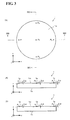
- a GaN substrate stored in a storage method of the present embodying mode has, referring to Fig. 2 and Fig. 3 , a planar first principal face 1 m , and its plane orientation in an arbitrary point P along the first principal face 1 m and separated 3 mm or more from the outer edge thereof (e.g., Point P c , Point P 1 , Point P 2 , Point P 3 , Point P 4 , etc.) has an off-inclination angle ⁇ of-10° or more, 10° or less with respect to the plane orientation of an arbitrarily designated crystalline plane 1 a that is inclined 50° or more, 90° or less (in Fig. 2 , inclination angle ⁇ ) with respect to a plane 1 c , being either the (0001) plane or the (000 1 ) plane, through the arbitrary point P .
- a GaN substrate in the present embodying mode because (i) it has a planar first principal face 1 m , and (ii) its plane orientation in an arbitrary point along the first principal face 1 m and separated 3 mm or more from the outer edge thereof has an off-inclination angle ⁇ of-10° or more, 10° or less with respect to the plane orientation of an arbitrarily designated crystalline plane 1 a that is inclined 50° or more, 90° or less with respect to a plane 1 c , being either the (0001) plane or the (000 1 ) plane, through the arbitrary point, by growing an at least single-lamina semiconductor layer onto the first principal face 1 m , a semiconductor device of minimal blue shift in photoemission and high emission efficiency is obtained.
- the off-inclination angle ⁇ of its plane orientation in an arbitrary point along the first principal face 1 m and separated 3 mm or more from the outer edge thereof is small, in the aforedescribed storing of the GaN substrate, inside the storing device reacting of oxygen and water vapor with the surfaces of the GaN substrate is controlled to a minimum, and the amount of oxygen and water-vapor adsorption onto the GaN substrate surfaces is reduced, whereby high-emission-efficiency semiconductor devices is obtained.
- the average roughness Ra of the first principal face 1 m is not greater than 20 nm, and the average roughness Ra of the second principal face 1 n is not greater than 20 ⁇ m. From such perspectives, it is more preferable that the average roughness Ra of the first principal face 1 m be 5 nm or less, and that the average roughness Ra of the second principal face 1 n be 10 ⁇ m or less.
- first principal face 1 m means the principal face on which semiconductor layers are grown
- second principal face 1 n means the principal face on the side opposite from said first principal face 1 m .
- average roughness Ra of a surface means arithmetic mean roughness Ra stipulated in JIS B 0601:200I, and refers to a value in which a predetermined reference surface area is chosen from the roughness topography along its average plane, and the absolute values of the deviation from the average plane of the chosen portion to the profiling topography are summed and the total is averaged in the reference surface area.
- Such surface average roughness Ra can be measured employing a non-contact interferometer, 3D-SEM (three-dimensional scanning electron micrometer), AFM (atomic-force microscope), or the like.
- the plane orientation of the foregoing arbitrarily designated crystalline plane 1 a preferably is ⁇ 20 2 1 ⁇ .
- a GaN substrate 1 in which the plane orientation in an arbitrary point P along the first principal face 1 m of the GaN substrate 1 and separated 3 mm or more from the outer edge thereof has an off-inclination angle ⁇ of -10° or more, 10° or less with respect to ⁇ 20 2 1 ⁇ , because semiconductor layers of high crystalline quality can be grown stably onto its first principal face 1 m , a semiconductor device of minimal blue shift in photoemission and high emission efficiency is obtained.
- the plane orientation in an arbitrary point P along the first principal face 1 m and separated 3 mm or more from the outer edge thereof e.g., Point P c , Point P 1 , Point P 2 , Point P 3 and Point P 4
- the plane orientation in an arbitrary point P along the first principal face 1 m and separated 3 mm or more from the outer edge thereof has an off-inclination angle ⁇ of-10° or more, 10° or less in a ⁇ 1 2 10> direction, and of -10° or more, 10° or less in a direction perpendicular to a ⁇ 20 2 1> direction and to a ⁇ 1 2 10> direction, more preferably has an off-inclination angle ⁇ of -3° or more, 3° or less in a ⁇ 1 2 10> direction with respect to ⁇ 20 2 1 ⁇ ,
- the off-inclination angle ⁇ between ⁇ 20 2 1 ⁇ and the plane orientation in an arbitrary point along the first principal face of the GaN substrate and separated 3 mm or more from the outer edge thereof can be measured by an XRD (x-ray diffraction) technique.
- the GaN substrates 1 can be stored by sealing the GaN substrates 1 into a (not-illustrated) storage container (e.g., an aluminum pouch or the like) that shuts out oxygen and water vapor. Further, GaN substrates hermetically sealed in a storage container can be taken out of the storing device 10 and stored.
- a (not-illustrated) storage container e.g., an aluminum pouch or the like
- GaN crystal 110 in which the off-angle between the plane orientation of the principal face of a sectional region 110 p of the GaN crystal 110 that grows onto the GaN parent-crystal piece 100 p , and the plane orientation of the principal face of a sectional region 110 q of the GaN crystal 110 that grows onto the GaN parent-crystal piece 100 q is -10° or more, 10° or less can be grown.
- the sectional regions 110 p and 110 q of the GaN crystal 110 are regions of the GaN crystal partitioned by planes (referred to as extension planes 110 t hereinafter) extending, into the GaN crystal 110 interior, the lateral sides 100 pt and 100 qt where the GaN parent-crystal pieces 100 p and 100 q adjoin each other.
- the off-inclination angle with respect to the aforementioned plane orientation ⁇ hkil ⁇ of the principal faces 100 pm and 100 qm of the plurality of GaN parent-crystal pieces 100 p and 100 q preferably is -10° or more, 10° or less, more preferably -3° or more, 3° or less, still more preferably -0.5° or more, 0.5° or less.
- the average roughness Ra of the principal faces 100 pm and 100 qm and lateral sides 100 pt and 100 qt of the GaN parent-crystal pieces 100 p and 100 q preferably is not grater than 50 nm, more preferably not greater than 5 nm.
- the method for growing the GaN crystal 110 while not particularly limited preferably is, from the perspective of growing GaN crystal of high crystalline quality, a vapor-phase method such as an HVPE (hydride vapor-phase epitaxy) technique, an MOCVD (metalorganic chemical vapor deposition) technique or an MBE (molecular-beam epitaxy) technique, or a liquid-phase method such as flux growth. From the perspective of the crystal growth rate being considerable, an HVPE technique is further preferable.
- HVPE hydrogen vapor-phase epitaxy
- MOCVD metalorganic chemical vapor deposition
- MBE molecular-beam epitaxy
- the crystal-growth conditions preferably are that the crystal-growth temperature is 950°C or more, 1200°C or less, and the crystal-growth rate is 30 ⁇ m/hr or more, 300 ⁇ m/hr or less.
- a step ( Fig. 6(D) ) of utilizing, as a GaN starting substrate 110 s , a GaN substrate 1 cut out from the grown GaN crystal 110 in planes 110 u and 110 v parallel to a plane of ⁇ hkil ⁇ plane orientation, and growing further GaN crystal 120 onto the principal face 110 pm of such GaN starting substrate 110 s , and a step ( Fig. 6(D) ) of cutting a GaN substrate 1 of Embodying Mode 1 out from the grown further GaN crystal 120 can further be included.
- further GaN crystal 120 in which the off-angle between the plane orientation of the principal face of a sectional region 120 p of the further GaN crystal 120 that grows onto the sectional region 110 p of the GaN starting substrate 110 s , and the plane orientation of the principal face of a sectional region 120 q of the further GaN crystal 120 that grows onto the sectional region 110 q of the GaN starting substrate 110 s is -10° or more, 10° or less can be grown.
- the sectional regions 120p and 120 q of the further GaN crystal 120 are regions of the further GaN crystal partitioned by planes (referred to as extension planes 120 t hereinafter) extending, into the further GaN crystal 120 interior, the extension planes 110 t of the GaN starting substrate 110 s .
- a GaN substrate 1 having a planar first principal face 1 m , and whose plane orientation in an arbitrary point along the first principal face 1 m and separated 3 mm or more from the outer edge thereof has an off-inclination angle of -10° or more, 10° or less with respect to the plane orientation of an arbitrarily designated crystalline plane that is inclined 50° or more, 90° or less with respect to a plane, being either the (0001) plane or the (000 1 ) plane, through the arbitrary point is obtained.
- the method for growing the further GaN crystal 120 while not particularly, limited preferably is, from the perspective of growing GaN crystal of high crystalline quality, a vapor-phase method such as an HVPE technique, an MOCVD technique or an MBE technique, or a liquid-phase method such as flux growth. From the perspective of the crystal growth rate being considerable, an HVPE technique is further preferable.
- the crystal-growth conditions preferably are that the crystal-growth temperature is 950°C or more, 1200°C or less, and the crystal-growth rate is 30 ⁇ m/hr or more, 300 ⁇ m/ hr or less.
- One mode of embodying a GaN substrate involving the present invention is a GaN substrate 1, stored within an atmosphere in which the oxygen concentration is not greater than 15 vol. % and the water-vapor concentration is not greater than 20 g/m 3 , having a planar first principal face 1 m , and whose plane orientation in an arbitrary point along the first principal face 1 m and separated 3 mm or more from the outer edge thereof has an off-inclination angle ⁇ of-10° or more, 10° or less with respect to the plane orientation of an arbitrarily designated crystalline plane 1 a that is inclined 50° or more, 90° or less with respect to a plane 1 c , being either the (0001) plane or the (000 1 ) plane, through the arbitrary point.
- One mode of embodying a semiconductor device involving the present invention includes a GaN substrate 1 of Embodying Mode 2, stored by a method of Embodying Mode 1, and an at least single-lamina semiconductor layer 210 formed onto the first principal face 1 m of the GaN substrate 1.
- a semiconductor device of the present embodying mode because a semiconductor layer 210 of high crystalline quality is formed onto the first principal face 1 m of a GaN substrate 1 in which oxidation of its surfaces has been kept to a minimum, a semiconductor device of superior properties is obtained.
- the semiconductor layer 210 formed onto the GaN substrate 1 there are no particular limitations on the semiconductor layer 210 formed onto the GaN substrate 1, but in view of the crystal lattices being highly coordinate, a Group III nitride semiconductor layer such as an Al x Ga y In 1- x-y N (0 ⁇ x, 0 ⁇ y , x + y ⁇ 1) layer is preferable.
- a Group III nitride semiconductor layer such as an Al x Ga y In 1- x-y N (0 ⁇ x, 0 ⁇ y , x + y ⁇ 1) layer is preferable.
- the semiconductor-layer formation method from the perspective of forming a semiconductor layer 210 of high crystalline quality onto the GaN substrate 1, it is preferable to employ an HVPE technique, an MOCVD technique or an MBE technique. From the viewpoint of allowing precise control of the thickness and chemical composition of the semiconductor layer 210 formed onto the GaN substrate 1, an MOCVD technique is further preferable.
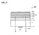
- an n -type GaN lamina 211, an In 0.2 Ga 0.8 N lamina 212, an Al 0.2 Ga 0.8 N lamina 213, and a p -type GaN lamina 214 are formed as the at least single-lamina semiconductor layer 210 in order onto the first principal face 1 m of a GaN substrate 1 of Embodying Mode 2, and further, onto the second principal face 1 n of the GaN substrate 1, an n -side electrode 221 is formed, and onto the principal face of the p -type GaN layer 214 a p -side electrode 222 is, wherein photoemission 230 is put out.
- One mode of embodying a method, involving the present invention, of manufacturing a semiconductor device includes a step of preparing a GaN substrate 1 of Embodying Mode 2, stored by a method of Embodying Mode 1, and a step of growing an at least single-lamina semiconductor layer 210 onto the first principal face 1 m of the GaN substrate 1. By such steps a semiconductor device of superior properties is obtained.
- a semiconductor-device manufacturing method of the present embodying mode includes the step of preparing a GaN substrate 1 of Embodying Mode 2, stored by a method of Embodying Mode 1. Such step of preparing a GaN substrate 1 is as set forth in Embodying Mode 1 and Embodying Mode 2.
- a semiconductor-device manufacturing method of the present embodying mode includes the step of growing an at least single-lamina semiconductor layer 210 onto the first principal face 1 m of the GaN substrate 1.
- the semiconductor layer 210 grown onto the GaN substrate while not particularly limited, preferably is, in view of the crystal lattices being highly coordinate, a Group III nitride semiconductor layer such as an Al x Ga y In 1- x - y N (0 ⁇ x, 0 ⁇ y, x + y ⁇ 1) layer.
- the semiconductor-layer growth method from the perspective of epitaxially growing the semiconductor layer 210 with ease onto the GaN substrate 1, it is preferable to employ an HVPE technique, an MOCVD technique or an MBE technique. From the viewpoint of allowing precise control of the thickness and chemical composition of the semiconductor layer 210 grown onto the GaN substrate 1, an MOCVD technique is further preferable.
- a semiconductor device manufacturing method of the present embodying mode referring to Fig. 4 and Fig. 5 , by for example growing, by means of an MOCVD technique, in order onto the first principal face 1 m of the GaN substrate 1 of Embodying Mode 2, an n -type GaN lamina 211, an In 0.2 Ga 0.8 N lamina 212, an Al 0.2 Ga 0.8 N lamina 213, and a p -type GaN lamina 214, as the at least single-lamina semiconductor layer 210, a semiconductor layer wafer 200 u is obtained.
- a semiconductor device 200 is obtained.
- the thus-obtained semiconductor device 200 puts out photoemission 230.
- Fig. 6(A) The (0001) side and the (0001) side-the two principal faces-of a GaN parent crystal 100 of 50.8 mm diameter and 3mm thickness, produced by an HVPE technique, were ground and polished to an average roughness Ra of the two principal faces of 5 nm.
- the average roughness Ra of the surfaces was characterized employing AFM.
- the GaN parent crystal 100 with the average roughness Ra of its two principal faces having been made 5 nm was sliced in a plurality of planes perpendicular to ⁇ 20 2 1> directions, whereby a plurality of GaN parent-crystal pieces 100 p and 100 q , having ⁇ 20 2 1 ⁇ principal faces, of 3.1 mm width, 20 to 50.8 mm length, and 1 mm thickness were cut from it.
- the not-ground and not-polished four sides of each cut-out GaN parent-crystal piece were ground and polished to bring the average roughness Ra of the four sides to 5 nm.
- GaN parent-crystal pieces whose ⁇ 20 2 1 ⁇ principal-face average roughness Ra was 5 nm were obtained.
- GaN parent-crystal pieces were GaN parent-crystal pieces whose principal-face plane orientation did not coincide with ⁇ 20 2 1 ⁇ , but even with any of such GaN parent-crystal pieces the off-inclination angle of its principal-face plane orientation with respect to ⁇ 20 2 1 ⁇ was -0.1 ° or more, 0.4° or less.
- the off-inclination angle was measured by x-ray diffractometry.
- these GaN parent-crystal pieces were arranged adjoining each other sideways inside the crystal-growth chamber of an HVPE apparatus, in such a way that the ⁇ 20 2 1 ⁇ principal faces 100 pm and 100 qm of the plurality of GaN parent-crystal pieces 100 p and 100 q paralleled each other, and in such a way that the [0001] directions of the GaN parent-crystal pieces 100 p and 100 q were identical.
- the average roughness Ra of the mutually adjoining lateral sides 100 pt and 100 qt of the plurality of GaN parent-crystal pieces 100 p and 100 q was 5 nm.
- the diameter of a circle inscribed on the outer periphery of, as whole, the plurality of GaN parent-crystal pieces 100 p and 100 q arranged in this way was 50.8 mm.
- the ⁇ 20 2 1 ⁇ principal faces 100 pm and 100 qm of the plurality of GaN parent-crystal pieces 100 p and 100 q arranged inside the crystal-growth chamber of the HVPE apparatus were treated two hours at 800°C under a mixed-gas atmosphere of 10 vol. % gaseous hydrogen chloride (NCl) and 90 vol.
- NCl gaseous hydrogen chloride
- the thickness of the obtained GaN crystal 110 was measured by a contact thickness gauge (a "Digimatic Indicator,” Mitutoyo Corp. mfr.), whereupon it was 4 mm. That meant that the crystal growth rate was 80 ⁇ m/hr. Referring to Fig. 6(C) , Fig. 2 and Fig.
- GaN substrates By cutting eight GaN substrates out of this GaN crystal 110 in planes 110 u and 1 10v parallel to a ⁇ 20 2 1 ⁇ plane, and carrying out grinding and polishing processes on their two principal faces, eight GaN substrates were obtained, of 50.8 mm diameter ⁇ 400 ⁇ m thickness, whose first principal-face 1 m average roughness Ra was 3 nm and whose second principal-face 1 n average roughness Ra was 8 ⁇ m, and whose off-inclination angle toward a ⁇ 1 2 10> direction (the x-axis direction in Fig. 3 ) and whose off-inclination angle toward a direction (the y-axis direction in Fig.
- Point P c is a point in the middle of the GaN substrate 1 on its first principal face 1 m
- Point P 1 , Point P 2 , Point P 3 and Point P 4 are each a point on the first principal face and separated 3 mm from the outer edge thereof, with Point P 1 , Point P c and Point P 2 lying in that order on a straight line in a ⁇ 1 2 10> direction and Point P 3 , Point P c and Point P 4 lying in that order on a straight line in a direction perpendicular to a ⁇ 20 2 1> direction and a ⁇ 1 2 10> direction.
- Each of seven GaN substrates within the eight GaN substrates obtained as above-described was washed and then stored for six months within an atmosphere having the oxygen concentrations and water-vapor concentrations set forth in Table 1-within atmospheres being a gaseous mixture of gaseous nitrogen as an inert gas, gaseous oxygen, and water vapor (Ex. I-1 through Ex. I-6 and Ex. I-R1).
- atmospheres being a gaseous mixture of gaseous nitrogen as an inert gas, gaseous oxygen, and water vapor.
- the remaining single GaN substrate, without undergoing storage of this sort, after the aforementioned production and washing of the GaN substrate was within 10 minutes placed inside the crystal-growth reaction chamber of an MOCVD apparatus, and semiconductor devices were fabricated as in the following (Ex. I-S).
- Point Q c , Point Q 1 , Point Q 2 , Point Q 3 and Point Q 4 on the principal face of the semiconductor layer 210 in the semiconductor wafer 200u are each positioned on a line normal to its first principal face through the Point P c , Point P 1 , Point P 2 , Point P 3 and Point P 4 on the first principal face 1 m of the GaN substrate 1.
- a 100-nm thick p-side electrode 222 was formed onto the principal face of the p-type GaN lamina 214, and then an 80- ⁇ m diameter x 100-nm thick n-side electrode 221 was formed onto the second principal face of the GaN substrate, to yield, as semiconductor devices 200, ten in each neighbor region for a total 40 LEDs of 500 ⁇ m ⁇ 500 ⁇ m geometry.
- the photoemission intensity of the 40 LEDs obtained in this way was measured by means of a spectral photometer, and their average photoemission intensities were computed.
- a plurality of GaN parent-crystal pieces was cut from a GaN parent crystal. With any of the cut-out GaN parent-crystal pieces, the off-inclination angle of its principal-face plane orientation with respect to ⁇ 20 2 1 ⁇ was -2° or more, 2° or less.
- the plurality of GaN parent crystals was arranged in the same way as with Embodiment Example I, and GaN crystal was grown by an HVPE technique onto their principal face.
- the GaN crystal was grown 40 hours under conditions in which the partial pressure of the hydrogen chloride gas that reacts with the Ga melt to generate the Ga chloride gas that is the Ga source-material gas was 3.3 kPa, the partial pressure of the ammonia (NH 3 ) gas that is the nitrogen source-material gas was 15.6 kPa, and the crystal-growth temperature was 1080°C.
- the obtained GaN crystal had 5 mm thickness. That meant that the crystal growth rate was 125 ⁇ m/hr.
- Each of seven GaN substrates within the eight GaN substrates obtained as above-described was washed and then stored for six months within an atmosphere having the oxygen concentrations and water-vapor concentrations set forth in Table II-within atmospheres being a gaseous mixture of gaseous nitrogen as an inert gas, gaseous oxygen, and water vapor (Ex. II-1 through Ex. II-6 and Ex. II-R1).
- the remaining single GaN substrate, without undergoing storage of this sort, after the aforementioned production and washing of the GaN substrate was within 10 minutes placed inside the crystal-growth reaction chamber of an MOCVD apparatus, and semiconductor devices were fabricated as in the following (Ex. II-S).
- a plurality of GaN parent-crystal pieces was cut from a GaN parent crystal. With any of the cut-out GaN parent-crystal pieces, the off-inclination angle of its principal-face plane orientation with respect to ⁇ 20 2 1 ⁇ was -5° or more, 5° or less.
- the plurality of GaN parent crystals was arranged in the same way as with Embodiment Example I, and GaN crystal was grown by an HVPE technique onto their principal face.
- the GaN crystal was grown 40 hours under conditions in which the partial pressure of the hydrogen chloride gas that reacts with the Ga melt to generate the Ga chloride gas that is the Ga source-material gas was 4.3 kPa, the partial pressure of the ammonia (NH 3 ) gas that is the nitrogen source-material gas was 15.6 kPa, and the crystal-growth temperature was 1080°C.
- the obtained GaN crystal had 6 mm thickness. That meant that the crystal growth rate was 150 ⁇ m/hr.
- Each of seven GaN substrates within the eight GaN substrates obtained as above-described was washed and then stored for six months within an atmosphere having the oxygen concentrations and water-vapor concentrations set forth in Table III-within atmospheres being a gaseous mixture of gaseous nitrogen as an inert gas, gaseous oxygen, and water vapor (Ex. III-1 through Ex. III-6 and Ex. III-R1).
- the remaining single GaN substrate, without undergoing storage of this sort, after the aforementioned production and washing of the GaN substrate was within 10 minutes placed inside the crystal-growth reaction chamber of an MOCVD apparatus, and semiconductor devices were fabricated as in the following (Ex. III-S).
- a plurality of GaN parent-crystal pieces was cut from a GaN parent crystal. With any of the cut-out GaN parent-crystal pieces, the off-inclination angle of its principal-face plane orientation with respect to ⁇ 20 2 1 ⁇ was -9° or more, 9° or less.
- the plurality of GaN parent crystals was arranged in the same way as with Embodiment Example I, and GaN crystal was grown by an HVPE technique onto their principal face.
- the GaN crystal was grown 40 hours under conditions in which the partial pressure of the hydrogen chloride gas that reacts with the Ga melt to generate the Ga chloride gas that is the Ga source-material gas was 6.4 kPa, the partial pressure of the ammonia (NH 3 ) gas that is the nitrogen source-material gas was 15.6 kPa, and the crystal-growth temperature was 1080°C.
- the obtained GaN crystal had 8 mm thickness. That meant that the crystal growth rate was 200 ⁇ m/hr.
- Each of seven GaN substrates within the eight GaN substrates obtained as above-described was washed and then stored for six months within an atmosphere having the oxygen concentrations and water-vapor concentrations set forth in Table IV-within atmospheres being a gaseous mixture of gaseous nitrogen as an inert gas, gaseous oxygen, and water vapor (Ex. IV-1 through Ex. IV-6 and Ex. IV-R1).
- the remaining single GaN substrate, without undergoing storage of this sort, after the aforementioned production and washing of the GaN substrate was within 10 minutes placed inside the crystal-growth reaction chamber of an MOCVD apparatus, and semiconductor devices were fabricated as in the following (Ex. IV-S).
- 1 GaN substrate; 1 a : crystalline plane; 1 c : plane being either the (0001) plane or the (0001) plane; 1 m , 1 n, 100 pm, 100 qm, 110 pm: principal faces; 10 : storing device; 20: gas introduction line; 23, 43: gases; 29: gas introduction valve; 31: oxygen scavenger; 32: dehydrating agent; 40: gas exhaust line; 49: gas exhaust valve; 100: GaN parent crystal; 100 p , 100 q : GaN parent-crystal pieces; 100 pt , 100 qt: lateral sides; 110, 120: GaN crystal; 110 p, 110 q , 120 p, 120q: sectional regions; 110 s : GaN starting substrate; 110 t, 120 t : extension planes; 110 u , 110 v, 120 u, 120 v : parallel planes; 200: semiconductor device; 200 u : semiconductor wafer; 210 : semiconductor layer; 211 n -type Ga
Landscapes
- Chemical & Material Sciences (AREA)
- Engineering & Computer Science (AREA)
- Crystallography & Structural Chemistry (AREA)
- Materials Engineering (AREA)
- Metallurgy (AREA)
- Organic Chemistry (AREA)
- Inorganic Chemistry (AREA)
- Crystals, And After-Treatments Of Crystals (AREA)
- Chemical Vapour Deposition (AREA)
- Led Devices (AREA)
Abstract
Description
- The present invention relates to methods of storing GaN substrates whose principal-face plane orientation is other than (0001) or (000
1 ), used to manufacture semiconductor devices, to such GaN substrates stored by the storing methods, to semiconductor devices in which an at least single-lamina semiconductor layer is formed onto the GaN substrates, and to methods of manufacturing such semiconductor devices. - Of late, in order to sustain, at a high level, photoemission efficiency in which blue-shift in the emission from LEDs (light-emitting diodes), LDs (laser diodes) and like semiconductor devices has been reduced, semipolar or nonpolar GaN substrates, whose principal-face plane orientation is other than (0001) or (0001), are being employed as the substrates for these semiconductor devices. "Nonpolar GaN substrates" signify GaN substrates having nonpolar faces as the principal faces, and specifically mean GaN substrates having principal faces of plane orientation inclined 90° (i.e., perpendicular) to the plane-either the (0001) plane or the (000
1 ) plane-that is the polar plane. "Semipolar GaN substrates" mean, specifically, GaN substrates having principal faces of plane orientation inclined greater than 0° and less than 90°to the plane-either the (0001) plane or the (0001 ) plane-that is the polar plane. - Therein, with the process whereby the GaN substrates are manufactured ordinarily being a process separate from the process whereby the manufactured GaN substrates are used to produce semiconductor devices, the manufactured GaN substrates are stored for a fixed time period, and thereafter used for producing the semiconductor devices. Therefore, in Japanese Unexamined Patent App. Pub. No.
2000-355392 - Therefore, in Japanese Unexamined Patent App. Pub. No.
2007-335583 1 ) plane-within an atmosphere in which the oxygen concentration and water-vapor concentration in air are controlled has been proposed. But if the aforementioned semipolar or nonpolar GaN substrates are stored by the method set forth in Japanese Unexamined Patent App. Pub. No.2007-335583 -
- PTL 1: Japanese Unexamined Pat. App. Pub. No.
2000-355392 - PTL 2: Japanese Unexamined Pat. App. Pub. No.
2007-335583 - An object of the present invention, to solve the problems discussed above, is to make available: a method of storing GaN substrates whose principal-face plane orientation is other than (0001) or (000
1 ), with which semiconductor devices of favorable properties can be manufactured; such GaN substrates stored by the storing method; semiconductor devices in which an at least single-lamina semiconductor layer is formed onto the GaN substrates; and a method of manufacturing such semiconductor devices. - The present invention, in accordance with a certain aspect thereof, is a GaN substrate storage method of storing, within an atmosphere in which the oxygen concentration is not greater than 15 vol. % and the water-vapor concentration is not greater than 20 g / m3, a GaN substrate having a planar first principal face, and whose plane orientation in an arbitrary point along the first principal face and separated 3 mm or more from the outer edge thereof has an off-inclination angle of-10° or more, 10° or less with respect to the plane orientation of an arbitrarily designated crystalline plane that is inclined 50° or more, 90° or less with respect to a plane, being either the (0001) plane or the (000
1 ) plane, through the arbitrary point. - In a GaN substrate storage method involving the present invention, the oxygen concentration can be made 10 vol. % or less, and the water-vapor concentration 15 g/m3 or less. Furthermore, the oxygen concentration can be brought to 6 vol. % or less, and the water-vapor concentration to 5 g/m3 or less. Likewise, the atmosphere under which the GaN substrates are stored can be formed from a gaseous mixture containing an inert gas, gaseous oxygen, and water vapor, with the oxygen concentration being made not less than 0.05 vol. % and the water-vapor concentration not less than 0.1 g/m3.
- Additionally, in a GaN substrate stored by a storing method involving the present invention, the average roughness Ra of a first principal face thereof can be made 20 nm or less, while the average roughness Ra of a second principal face thereof can be made 20 µm or less. Furthermore, the average roughness Ra of the first principal face can be brought to 5 nm or less, and the average roughness Ra of the second principal face to 10 µm or less.
- And in a GaN substrate stored by a storage method involving the present invention, it is possible to have the plane orientation of the arbitrarily designated crystalline plane be {20
2 1}. Therein, the plane orientation in an arbitrary point along the first principal face and separated 3 mm or more from the outer edge thereof can have an off-inclination angle of -10° or more, 10° or less in a <12 10> direction with respect to {202 1}, and of -10° or more, 10° or less in a direction perpendicular to a <202 1> direction and to a <12 10> direction. Likewise, the plane orientation in an arbitrary point along the first principal face and separated 3 mm or more from the outer edge thereof can have an off-inclination angle of-3° or more, 3° or less in a <12 10> direction with respect to {202 1}, and of -3° or more, 3° or less in a direction perpendicular to a <202 1> direction and to a <12 10> direction. Furthermore, the plane orientation in an arbitrary point along the first principal face and separated 3 mm or more from the outer edge thereof can have an off-inclination angle of-0.5° or more, 0.5° or less in a <12 10> direction with respect to {202 1}, and of -0.5° or more, 0.5° or less in a direction perpendicular to a <202 1> direction and to a <12 10> direction. - The present invention in accordance with a separate aspect is a GaN substrate stored within an atmosphere in which the oxygen concentration is not greater than 15 vol. % and the water-vapor concentration is not greater than 20 g / m3, having a planar first principal face, and whose plane orientation in an arbitrary point along the first principal face and separated 3 mm or more from the outer edge thereof has an off-inclination angle of -10° or more, 10° or less with respect to the plane orientation of an arbitrarily designated crystalline plane that is inclined 50° or more, 90° or less with respect to a plane, being either the (0001) plane or the (000
1 ) plane, through the arbitrary point. - And the present invention in accordance with a still separate aspect is a semiconductor device including an above-described GaN substrate, and an at least single-lamina semiconductor layer formed onto the first principal face of the GaN substrate. The present invention is also a semiconductor device manufacturing method including a step of preparing an above-described GaN substrate, and a step of growing an at least single-lamina semiconductor layer onto the first principal face of the GaN substrate.
- The present invention affords: a method of storing GaN substrates whose principal-face plane orientation is other than (0001) or (000
1 ), with which semiconductor devices of favorable properties can be manufactured; such GaN substrates stored by the storing method; semiconductor devices in which an at least single-lamina semiconductor layer is formed onto the GaN substrates; and a method of manufacturing such semiconductor devices. -
-
Fig. 1 is a schematic diagram representing one mode of embodying a GaN substrate storage method involving the present invention. -
Fig. 2 is a schematic diagram representing one mode of embodying a GaN substrate involving the present invention. -
Fig. 3 is a simplified diagram specifically representing one mode of embodying a GaN substrate involving the present invention. Therein, (A) depicts a simplified plan view of the GaN substrate, (B) depicts a simplified sectional view along IIIB - IIIB in (A), and (C) depicts a simplified sectional view along IIIC - IIIC in (A). -
Fig. 4 is a simplified diagram specifically representing one mode of embodying a semiconductor device including a GaN substrate involving the present invention. Therein, (A) depicts a simplified plan view of the GaN substrate, and (B) depicts a simplified sectional view along IVB - IVB in (A). -
Fig. 5 is a simplified sectional diagram representing one mode of embodying a semiconductor device involving the present invention. -
Fig. 6 is a simplified diagram representing a method of manufacturing a GaN substrate involving the present invention. Therein, (A) represents an operation of cutting a plurality of GaN parent-crystal pieces from a GaN parent crystal, (B) represents an operation of arranging a plurality of GaN parent-crystal pieces adjoining each other sideways, (C) represents an operation of growing GaN crystal onto the plurality of parent-crystal GaN pieces and cutting out a GaN substrate, and (D) represents a further operation of growing GaN crystal and cutting out a GaN substrate. -
Fig. 7 is a graph charting one example of the relationship between semiconductor device properties, and oxygen concentration and water-vapor concentration in an atmosphere for storing GaN substrates. -
Fig. 8 is a graph charting another example of the relationship between semiconductor device properties, and oxygen concentration and water-vapor concentration in an atmosphere for storing GaN substrates. -
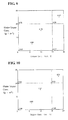
Fig. 9 is a graph charting a further example of the relationship between semiconductor device properties, and oxygen concentration and water-vapor concentration in an atmosphere for storing GaN substrates. -
Fig. 10 is a graph charting a still further example of the relationship between semiconductor device properties, and oxygen concentration and water-vapor concentration in an atmosphere for storing GaN substrates. - In crystallography, in order to express the plane orientation of crystalline planes, notation (Miller notation) such as (hkl) or (hkil) is used. The plane orientation of crystalline planes in Group 111-nitride crystal and other hexagonal-system crystal constituting GaN parent crystal, GaN parent-crystal pieces, GaN crystal, GaN substrates, etc., is expressed by (hkil). Herein, h, k, i and l are integers referred to as Miller indices, and have the relationship i = -(h + k). A plane of (hkil) plane orientation is called an (hkil) plane. Likewise, the direction perpendicular to the (hkil) plane (the direction normal to the (hkil) plane) is called the [hkil] direction. And {hkil} signifies a family of plane orientations that includes (hkil) and the individual plane orientations that are its crystallographic equivalent, while <hkil> signifies a family of directions that includes [hkik] and the individual directions that are its crystallographic equivalent.
- Reference is made to
Fig. 1 and Fig. 2 : One mode of embodying a GaN substrate storage method involving the present invention stores, within an atmosphere in which the oxygen concentration is not greater than 15 vol. % and the water-vapor concentration is not greater than 20 g/m3, aGaN substrate 1 having a planar firstprincipal face 1m, and whose plane orientation in an arbitrary point P along the firstprincipal face 1m and separated 3 mm or more from the outer edge thereof has an off-inclination angle (inFig. 2 , off-inclination angle Δα) of-10° or more, 10° or less with respect to the plane orientation of an arbitrarily designatedcrystalline plane 1a that is inclined 50° or more, 90° or less (inFig. 2 , inclination angle α) with respect to a plane, being either the (0001) plane or the (0001 ) plane, through the arbitrary point P. - Storing the aforedescribed GaN substrates under the atmosphere in which the oxygen concentration is not greater than 15 vol. % and the water-vapor concentration is not greater than 20 g/m3 makes it possible to keep oxidation of the GaN substrate surfaces to a minimum, enabling the manufacture of semiconductor devices of favorable properties. From such perspectives, the oxygen concentration is preferably not greater than 10 vol. % and the water-vapor concentration not greater than 15 g/m3, and more preferably, the oxygen concentration is not greater than 6 vol. % and the water-vapor concentration is not greater than 5 g / m3. On the other hand, from the perspective of reducing the cost of creating the atmosphere for storing the GaN substrates, preferably the oxygen concentration is 0.05 vol. % or more and the water-vapor concentration is 0.1 g/m3 or more.
- Herein, the technique whereby in the atmosphere for storing the above-described GaN substrates the oxygen concentration is made not greater than 15 vol. % and the water-vapor concentration is made not greater than 20 g/m3 is not particularly limited, wherein a
storing device 10 as represented inFig. 1 may for example be employed. Therein, the storingdevice 10 inFig. 1 is equipped with agas introduction line 20, agas introduction valve 29, agas exhaust line 40, and agas exhaust valve 49. - As a way to have the oxygen concentration be no more than 15 vol. % and the water-vapor concentration be no more than 20 g /m3 in an atmosphere for storing the aforedescribed GaN substrates, one technique (referred to as "Technique I"-likewise below) is, with
GaN substrates 1 placed inside the storingdevice 10, to introducelow gas 23 of oxygen concentration not greater than 15 vol. % and water-vapor concentration not greater than 20 g/m3 into the storingdevice 10, exhaustinggas 43 of oxygen concentration higher than 15 vol. % as well as water-vapor concentration higher than 20 g/m3. Another technique (referred to as "Technique II"-likewise below) is to place, together with theGaN substrates 1, anoxygen scavenger 31 and a dehydrating agent 32 a inside the storingdevice 10. Moreover, Technique I and Technique II can be employed in tandem. - Herein, the gas whose oxygen concentration and water-vapor concentration are, respectively, not greater than 15 vol. % and not greater than 20 g/m3 is not particularly limited, but from the perspective of not causing chemical reactions with the surfaces of the GaN substrates, other than an inert gas such as gaseous nitrogen or gaseous argon, gaseous mixtures containing these inert gases and a predetermined quantity or less of gaseous oxygen and water vapor are preferable. In particular, from a low-cost perspective, a just-mentioned gaseous mixture of an inert gas and gaseous oxygen and water vapor, being a gaseous mixture whose oxygen concentration and water-vapor concentration are, respectively, not greater than 15 vol. % and not greater than 20 g/m3, is preferable. Also, the oxygen scavenger is not particularly limited, but from the perspective of not causing chemical reactions with the GaN substrate surfaces, active iron oxide, activated carbon, or the like is preferable. Likewise, while the dehydrating agent is not particularly limited, from the perspective of not causing chemical reactions with the GaN substrate surfaces, silica gel, activated carbon, or the like is preferable.
- Furthermore, the measuring of the oxygen concentration is not particularly limited, but can be carried out by means of a galvanic oxygen analyzer. Likewise, the measuring of the water-vapor concentration is not particularly limited, but may be carried out by means of a dielectric aquameter or a Karl Fischer moisture analyzer.
- The temperature of the atmosphere for storing the GaN substrates is also not particularly limited, but from the perspective of not causing chemical reactions with the surface of the GaN substrates, it is preferably not greater than 60°C, with not greater than 40°C being more preferable. In addition, from the perspective of preventing condensation, 5°C or greater is preferable, with 10°C or greater being more preferable.
- A GaN substrate stored in a storage method of the present embodying mode has, referring to
Fig. 2 andFig. 3 , a planar firstprincipal face 1m, and its plane orientation in an arbitrary point P along the firstprincipal face 1m and separated 3 mm or more from the outer edge thereof (e.g., Point Pc , Point P1 , Point P2 , Point P3 , Point P4 , etc.) has an off-inclination angle Δα of-10° or more, 10° or less with respect to the plane orientation of an arbitrarily designatedcrystalline plane 1a that is inclined 50° or more, 90° or less (inFig. 2 , inclination angle α) with respect to aplane 1c, being either the (0001) plane or the (0001 ) plane, through the arbitrary point P. - With a GaN substrate in the present embodying mode, because (i) it has a planar first
principal face 1m, and (ii) its plane orientation in an arbitrary point along the firstprincipal face 1m and separated 3 mm or more from the outer edge thereof has an off-inclination angle Δα of-10° or more, 10° or less with respect to the plane orientation of an arbitrarily designatedcrystalline plane 1a that is inclined 50° or more, 90° or less with respect to aplane 1c, being either the (0001) plane or the (0001 ) plane, through the arbitrary point, by growing an at least single-lamina semiconductor layer onto the firstprincipal face 1m, a semiconductor device of minimal blue shift in photoemission and high emission efficiency is obtained. In particular, because the off-inclination angle Δα of its plane orientation in an arbitrary point along the firstprincipal face 1m and separated 3 mm or more from the outer edge thereof is small, in the aforedescribed storing of the GaN substrate, inside the storing device reacting of oxygen and water vapor with the surfaces of the GaN substrate is controlled to a minimum, and the amount of oxygen and water-vapor adsorption onto the GaN substrate surfaces is reduced, whereby high-emission-efficiency semiconductor devices is obtained. - Furthermore, as for GaN substrates of the present embodying mode, from the perspectives of keeping reaction of oxygen and water vapor inside the storing device with the GaN substrate surfaces under control, and of reducing the amount of oxygen and water-vapor adsorption into the GaN substrate surfaces, preferably the average roughness Ra of the first
principal face 1m is not greater than 20 nm, and the average roughness Ra of the secondprincipal face 1n is not greater than 20 µm. From such perspectives, it is more preferable that the average roughness Ra of the firstprincipal face 1m be 5 nm or less, and that the average roughness Ra of the secondprincipal face 1n be 10 µm or less. Although the relationship between the average roughness Ra of firstprincipal face 1m and secondprincipal face 1n of theGaN substrate 1 and the reactivity and adsorptivity of oxygen and water vapor with these principal faces 1m and 1n of theGaN substrate 1 is not clear, the reduction in surface area from lessening the average roughness Ra is believed to be relevant as one causative factor. Herein, the "firstprincipal face 1m" means the principal face on which semiconductor layers are grown, while the "secondprincipal face 1n" means the principal face on the side opposite from said firstprincipal face 1m. Furthermore, "average roughness Ra of a surface" means arithmetic mean roughness Ra stipulated in JIS B 0601:200I, and refers to a value in which a predetermined reference surface area is chosen from the roughness topography along its average plane, and the absolute values of the deviation from the average plane of the chosen portion to the profiling topography are summed and the total is averaged in the reference surface area. Such surface average roughness Ra can be measured employing a non-contact interferometer, 3D-SEM (three-dimensional scanning electron micrometer), AFM (atomic-force microscope), or the like. - With further regard to a GaN substrate of the present embodying mode, referring to
Fig. 2 , the plane orientation of the foregoing arbitrarily designatedcrystalline plane 1a preferably is {202 1}. With aGaN substrate 1 in which the plane orientation in an arbitrary point P along the firstprincipal face 1m of theGaN substrate 1 and separated 3 mm or more from the outer edge thereof has an off-inclination angle Δα of -10° or more, 10° or less with respect to {202 1}, because semiconductor layers of high crystalline quality can be grown stably onto its firstprincipal face 1m, a semiconductor device of minimal blue shift in photoemission and high emission efficiency is obtained. - Further in respect of a GaN substrate of the present embodying mode, referring to
Fig. 2 andFig. 3 , from the perspectives of keeping oxygen and water vapor inside the storing device from reacting with the GaN substrate surfaces, and of reducing the amount of oxygen and water-vapor adsorption into the GaN substrate surfaces, preferably the plane orientation in an arbitrary point P along the first principal face 1m and separated 3 mm or more from the outer edge thereof (e.g., Point Pc , Point P1 , Point P2 , Point P3 and Point P4 ) has an off-inclination angle Δα of-10° or more, 10° or less in a <12 10> direction, and of -10° or more, 10° or less in a direction perpendicular to a <202 1> direction and to a <12 10> direction, more preferably has an off-inclination angle Δα of -3° or more, 3° or less in a <12 10> direction with respect to {202 1}, and of-3° or more, 3° or less in a direction perpendicular to a <202 1> direction and to a <1 2 10> direction, and still more preferably has an off-inclination angle of-0.5° or more, 0.5° or less in a <12 10> direction with respect to {202 1}, and of -0.5° or more, 0.5° or less in a direction perpendicular to a <202 1> direction and to a <12 10> direction. - While the relationship between the off-inclination angle Δα between {20
2 1} and the plane orientation in an arbitrary point along the firstprincipal face 1m of theGaN substrate 1 and separated 3 mm or more from the outer edge thereof, and the reactivity and adsorptivity of oxygen and water vapor with respect to the firstprincipal face 1m of theGaN substrate 1 is not clear, what is believed to be relevant as one causative factor is that having a predetermined off-inclination angle Δα varies the number of sites along the firstprincipal face 1m of theGaN substrate 1 where oxygen and water vapor may bond. The off-inclination angle Δα between {202 1} and the plane orientation in an arbitrary point along the first principal face of the GaN substrate and separated 3 mm or more from the outer edge thereof can be measured by an XRD (x-ray diffraction) technique. - Here, in the present embodying mode, referring to
Fig. 1 , with the atmosphere inside the storingdevice 10 in which theGaN substrates 1 are housed having been rendered storing conditions in the invention of the present application (for example, that the oxygen concentration be not greater than 15 vol. % and the water-vapor concentration be not greater than 20 g / m3), theGaN substrates 1 can be stored by sealing theGaN substrates 1 into a (not-illustrated) storage container (e.g., an aluminum pouch or the like) that shuts out oxygen and water vapor. Further, GaN substrates hermetically sealed in a storage container can be taken out of the storingdevice 10 and stored. - With reference to
Fig. 6 , in a GaN substrate manufacturing method of the present embodying mode, while not particularly limited, included are: a step (Fig. 6(A) ) of cutting from a GaN parent crystal 100 a plurality of GaN parent-crystal pieces 100p and 100q having principal faces 100pm and 100qm whose off-inclination angle is -5° or more, 5° or less with respect to a plane orientation {hkil} having an inclination angle α of 50° or more, 90° or less with respect to a plane, being either the (0001) plane or the (0001 ) plane, of the GaN parent crystal; a step (Fig. 6(B) ) of arranging the GaN parent-crystal pieces 100p and 100q adjoining each other sideways in such a way that the principal faces 100pm and 100qm of the GaN parent-crystal pieces 100p and 100q parallel each other, and the [0001] directions of the GaN parent-crystal pieces 100p and 100q are identical; a step (Fig. 6(C) ) of growing GaN crystal 110 onto the principal faces 100pm and 100qm of the GaN parent-crystal pieces 100p and 100q; and a step (Fig. 6(C) ) of cutting out a GaN substrate 1 of Embodying Mode 1 from the grown GaN crystal 110. - In the above-described steps,
GaN crystal 110 in which the off-angle between the plane orientation of the principal face of asectional region 110p of theGaN crystal 110 that grows onto the GaN parent-crystal piece 100p, and the plane orientation of the principal face of asectional region 110q of theGaN crystal 110 that grows onto the GaN parent-crystal piece 100q is -10° or more, 10° or less can be grown. Herein, thesectional regions GaN crystal 110 are regions of the GaN crystal partitioned by planes (referred to as extension planes 110t hereinafter) extending, into theGaN crystal 110 interior, the lateral sides 100pt and 100qt where the GaN parent-crystal pieces - By cutting the thus-obtained
GaN crystal 110 inplanes GaN substrate 1 having a planar firstprincipal face 1m, and whose plane orientation in an arbitrary point along the firstprincipal face 1m and separated 3 mm or more from the outer edge thereof has an off-inclination angle of -10° or more, 10° or less with respect to the plane orientation of an arbitrarily designated crystalline plane that is inclined 50° or more, 90° or less with respect to a plane, being either the (0001) plane or the (0001 ) plane, through the arbitrary point is obtained. - Therein, from the perspective of making the off-inclination angle through the aforementioned arbitrary point in the
GaN substrate 1 small, the off-inclination angle with respect to the aforementioned plane orientation {hkil} of the principal faces 100pm and 100qm of the plurality of GaN parent-crystal pieces crystal pieces - And the method for growing the
GaN crystal 110, while not particularly limited preferably is, from the perspective of growing GaN crystal of high crystalline quality, a vapor-phase method such as an HVPE (hydride vapor-phase epitaxy) technique, an MOCVD (metalorganic chemical vapor deposition) technique or an MBE (molecular-beam epitaxy) technique, or a liquid-phase method such as flux growth. From the perspective of the crystal growth rate being considerable, an HVPE technique is further preferable. If theGaN crystal 110 is grown by an HVPE technique, from the perspective of making the off-inclination angle through the aforementioned arbitrary point in theGaN substrate 1 small, the crystal-growth conditions preferably are that the crystal-growth temperature is 950°C or more, 1200°C or less, and the crystal-growth rate is 30 µm/hr or more, 300 µm/hr or less. - In a method of manufacturing a GaN substrate of the present embodying mode, a step (
Fig. 6(D) ) of utilizing, as aGaN starting substrate 110s, aGaN substrate 1 cut out from the grownGaN crystal 110 inplanes further GaN crystal 120 onto the principal face 110pm of suchGaN starting substrate 110s, and a step (Fig. 6(D) ) of cutting aGaN substrate 1 of EmbodyingMode 1 out from the grownfurther GaN crystal 120 can further be included. - By the above-described steps,
further GaN crystal 120 in which the off-angle between the plane orientation of the principal face of asectional region 120p of thefurther GaN crystal 120 that grows onto thesectional region 110p of theGaN starting substrate 110s, and the plane orientation of the principal face of asectional region 120q of thefurther GaN crystal 120 that grows onto thesectional region 110q of theGaN starting substrate 110s is -10° or more, 10° or less can be grown. Herein, thesectional regions further GaN crystal 120 are regions of the further GaN crystal partitioned by planes (referred to as extension planes 120t hereinafter) extending, into thefurther GaN crystal 120 interior, the extension planes 110t of theGaN starting substrate 110s. - By cutting the thus-obtained
further GaN crystal 120 inplanes GaN substrate 1 having a planar firstprincipal face 1m, and whose plane orientation in an arbitrary point along the firstprincipal face 1m and separated 3 mm or more from the outer edge thereof has an off-inclination angle of -10° or more, 10° or less with respect to the plane orientation of an arbitrarily designated crystalline plane that is inclined 50° or more, 90° or less with respect to a plane, being either the (0001) plane or the (0001 ) plane, through the arbitrary point is obtained. - The method for growing the
further GaN crystal 120, while not particularly, limited preferably is, from the perspective of growing GaN crystal of high crystalline quality, a vapor-phase method such as an HVPE technique, an MOCVD technique or an MBE technique, or a liquid-phase method such as flux growth. From the perspective of the crystal growth rate being considerable, an HVPE technique is further preferable. If thefurther GaN crystal 120 is grown by an HVPE technique, from the perspective of making the off-inclination angle through the aforementioned arbitrary point in theGaN substrate 1 small, the crystal-growth conditions preferably are that the crystal-growth temperature is 950°C or more, 1200°C or less, and the crystal-growth rate is 30 µm/hr or more, 300 µm/ hr or less. - Reference is made to
Fig. 1 through Fig. 3 : One mode of embodying a GaN substrate involving the present invention is aGaN substrate 1, stored within an atmosphere in which the oxygen concentration is not greater than 15 vol. % and the water-vapor concentration is not greater than 20 g/m3, having a planar firstprincipal face 1m, and whose plane orientation in an arbitrary point along the firstprincipal face 1m and separated 3 mm or more from the outer edge thereof has an off-inclination angle Δα of-10° or more, 10° or less with respect to the plane orientation of an arbitrarily designatedcrystalline plane 1a that is inclined 50° or more, 90° or less with respect to aplane 1c, being either the (0001) plane or the (0001 ) plane, through the arbitrary point. With a GaN substrate of the present embodying mode, stored by a method of EmbodyingMode 1, because surface oxidation is kept to a minimum, by growing an at least single-lamina semiconductor layer onto the firstprincipal face 1m, a semiconductor device of superior properties is obtained. - Reference is made to
Fig. 4 andFig. 5 : One mode of embodying a semiconductor device involving the present invention includes aGaN substrate 1 of Embodying Mode 2, stored by a method of EmbodyingMode 1, and an at least single-lamina semiconductor layer 210 formed onto the firstprincipal face 1m of theGaN substrate 1. With a semiconductor device of the present embodying mode, because asemiconductor layer 210 of high crystalline quality is formed onto the firstprincipal face 1m of aGaN substrate 1 in which oxidation of its surfaces has been kept to a minimum, a semiconductor device of superior properties is obtained. - There are no particular limitations on the
semiconductor layer 210 formed onto theGaN substrate 1, but in view of the crystal lattices being highly coordinate, a Group III nitride semiconductor layer such as an Al x Ga y In1-x-y N (0 ≤ x, 0 ≤ y, x + y ≤ 1) layer is preferable. Likewise, while there are no particular limitations on the semiconductor-layer formation method, from the perspective of forming asemiconductor layer 210 of high crystalline quality onto theGaN substrate 1, it is preferable to employ an HVPE technique, an MOCVD technique or an MBE technique. From the viewpoint of allowing precise control of the thickness and chemical composition of thesemiconductor layer 210 formed onto theGaN substrate 1, an MOCVD technique is further preferable. - With a semiconductor device of the present embodying mode, referring to
Fig. 4 andFig. 5 , specifically an n-type GaN lamina 211, an In0.2Ga0.8N lamina 212, an Al0.2Ga0.8N lamina 213, and a p-type GaN lamina 214 are formed as the at least single-lamina semiconductor layer 210 in order onto the firstprincipal face 1m of aGaN substrate 1 of Embodying Mode 2, and further, onto the secondprincipal face 1n of theGaN substrate 1, an n-side electrode 221 is formed, and onto the principal face of the p-type GaN layer 214 a p-side electrode 222 is, whereinphotoemission 230 is put out. - Reference is made to
Fig. 3 through Fig. 5 : One mode of embodying a method, involving the present invention, of manufacturing a semiconductor device includes a step of preparing aGaN substrate 1 of Embodying Mode 2, stored by a method of EmbodyingMode 1, and a step of growing an at least single-lamina semiconductor layer 210 onto the firstprincipal face 1m of theGaN substrate 1. By such steps a semiconductor device of superior properties is obtained. - A semiconductor-device manufacturing method of the present embodying mode, referring to
Fig. 3 through Fig. 5 , includes the step of preparing aGaN substrate 1 of Embodying Mode 2, stored by a method of EmbodyingMode 1. Such step of preparing aGaN substrate 1 is as set forth in EmbodyingMode 1 and Embodying Mode 2. - A semiconductor-device manufacturing method of the present embodying mode, referring to
Fig. 4 andFig. 5 , includes the step of growing an at least single-lamina semiconductor layer 210 onto the firstprincipal face 1m of theGaN substrate 1. Thesemiconductor layer 210 grown onto theGaN substrate 1, while not particularly limited, preferably is, in view of the crystal lattices being highly coordinate, a Group III nitride semiconductor layer such as an Al x Ga y In1-x-y N (0 ≤ x, 0 ≤ y, x + y ≤ 1) layer. Likewise, while there are no particular limitations on the semiconductor-layer growth method, from the perspective of epitaxially growing thesemiconductor layer 210 with ease onto theGaN substrate 1, it is preferable to employ an HVPE technique, an MOCVD technique or an MBE technique. From the viewpoint of allowing precise control of the thickness and chemical composition of thesemiconductor layer 210 grown onto theGaN substrate 1, an MOCVD technique is further preferable. - With a semiconductor device manufacturing method of the present embodying mode, referring to
Fig. 4 andFig. 5 , by for example growing, by means of an MOCVD technique, in order onto the firstprincipal face 1m of theGaN substrate 1 of Embodying Mode 2, an n-type GaN lamina 211, an In0.2Ga0.8N lamina 212, an Al0.2Ga0.8N lamina 213, and a p-type GaN lamina 214, as the at least single-lamina semiconductor layer 210, asemiconductor layer wafer 200u is obtained. Subsequently, by forming an n-side electrode 221 onto the secondprincipal face 1n of theGaN substrate 1 in thesemiconductor layer wafer 200u, and forming a p-side electrode 222 onto the principal face of the p-type GaN layer 214, asemiconductor device 200 is obtained. The thus-obtainedsemiconductor device 200 puts outphotoemission 230. - Reference is made to
Fig. 6(A) : The (0001) side and the (0001) side-the two principal faces-of aGaN parent crystal 100 of 50.8 mm diameter and 3mm thickness, produced by an HVPE technique, were ground and polished to an average roughness Ra of the two principal faces of 5 nm. Herein, the average roughness Ra of the surfaces was characterized employing AFM. - Subsequently, the
GaN parent crystal 100 with the average roughness Ra of its two principal faces having been made 5 nm was sliced in a plurality of planes perpendicular to <202 1> directions, whereby a plurality of GaN parent-crystal pieces 2 1} principal faces, of 3.1 mm width, 20 to 50.8 mm length, and 1 mm thickness were cut from it. Following that, the not-ground and not-polished four sides of each cut-out GaN parent-crystal piece were ground and polished to bring the average roughness Ra of the four sides to 5 nm. Thus, a plurality of GaN parent-crystal pieces whose {202 1} principal-face average roughness Ra was 5 nm were obtained. Among these GaN parent-crystal pieces were GaN parent-crystal pieces whose principal-face plane orientation did not coincide with {202 1}, but even with any of such GaN parent-crystal pieces the off-inclination angle of its principal-face plane orientation with respect to {202 1} was -0.1 ° or more, 0.4° or less. Herein, the off-inclination angle was measured by x-ray diffractometry. - Next, referring to
Fig. 6(B) , these GaN parent-crystal pieces were arranged adjoining each other sideways inside the crystal-growth chamber of an HVPE apparatus, in such a way that the {202 1} principal faces 100pm and 100qm of the plurality of GaN parent-crystal pieces crystal pieces crystal pieces crystal pieces - Next, referring to
Fig. 6(C) , the {202 1} principal faces 100pm and 100qm of the plurality of GaN parent-crystal pieces GaN crystal 110 was grown 50 hours by an HVPE technique onto the principal faces 100pm and 100qm under conditions in which the partial pressure of the hydrogen chloride gas that reacts with the Ga melt to generate the Ga chloride gas that is the Ga source-material gas was 2.2 kPa, the partial pressure of the ammonia (NH3) gas that is the nitrogen source-material gas was 15.6 kPa, and the crystal-growth temperature was 1080°C. - The thickness of the obtained
GaN crystal 110 was measured by a contact thickness gauge (a "Digimatic Indicator," Mitutoyo Corp. mfr.), whereupon it was 4 mm. That meant that the crystal growth rate was 80 µm/hr. Referring toFig. 6(C) ,Fig. 2 andFig. 3 : By cutting eight GaN substrates out of thisGaN crystal 110 inplanes 2 1} plane, and carrying out grinding and polishing processes on their two principal faces, eight GaN substrates were obtained, of 50.8 mm diameter × 400 µm thickness, whose first principal-face 1m average roughness Ra was 3 nm and whose second principal-face 1n average roughness Ra was 8 µm, and whose off-inclination angle toward a <12 10> direction (the x-axis direction inFig. 3 ) and whose off-inclination angle toward a direction (the y-axis direction inFig. 3 ) perpendicular to a <2022 1> direction and a <12 10> direction-being the off-inclination angles between the first principal face and a {202 1} plane in each of points, along the firstprincipal face 1m, Point Pc, Point P 1, Point P2 , Point P3 and Point P4 -are each entered in Table I. - Herein, referring to
Fig. 3 , Point Pc, is a point in the middle of theGaN substrate 1 on its firstprincipal face 1m, while Point P1 , Point P2 , Point P3 and Point P4 are each a point on the first principal face and separated 3 mm from the outer edge thereof, with Point P1 , Point Pc and Point P2 lying in that order on a straight line in a <12 10> direction and Point P3 , Point Pc and Point P4 lying in that order on a straight line in a direction perpendicular to a <202 1> direction and a <12 10> direction. - Each of seven GaN substrates within the eight GaN substrates obtained as above-described was washed and then stored for six months within an atmosphere having the oxygen concentrations and water-vapor concentrations set forth in Table 1-within atmospheres being a gaseous mixture of gaseous nitrogen as an inert gas, gaseous oxygen, and water vapor (Ex. I-1 through Ex. I-6 and Ex. I-R1). The remaining single GaN substrate, without undergoing storage of this sort, after the aforementioned production and washing of the GaN substrate was within 10 minutes placed inside the crystal-growth reaction chamber of an MOCVD apparatus, and semiconductor devices were fabricated as in the following (Ex. I-S).
- Referring to
Fig. 4 andFig. 5 : The foregoing seven GaN substrates following storage (Ex. I-1 through Ex. I-6 and Ex. I-R1) and the non-stored single GaN substrate (Ex. I-S) were each placed inside the crystal-growth reaction chamber of an MOCVD apparatus, and a 5-µm thick n-type GaN lamina 211, a 3-nm thick In0.2Ga0.8N lamina 212, a 60-nm thick Al0.2Ga0.8N lamina 213, and a 150-nm thick p-type GaN lamina 214 were grown in order, as thesemiconductor layer 210, onto the firstprincipal face 1m of eachGaN substrate 1 to yield asemiconductor wafer 200u. Herein, Point Qc, Point Q1, Point Q2 , Point Q3 and Point Q4 on the principal face of thesemiconductor layer 210 in thesemiconductor wafer 200u are each positioned on a line normal to its first principal face through the Point Pc, Point P1 , Point P2 , Point P3 and Point P4 on the firstprincipal face 1m of theGaN substrate 1. - As indicated in
Fig. 4 , in four neighbor regions of Point Q1 , Point Q2 , Point Q3 and Point Q4 of 5 mm width, separated 3 mm to 10 mm from the outer edge of the principal face of thesemiconductor wafer 200u, a 100-nm thick p-side electrode 222 was formed onto the principal face of the p-type GaN lamina 214, and then an 80-µm diameter x 100-nm thick n-side electrode 221 was formed onto the second principal face of the GaN substrate, to yield, assemiconductor devices 200, ten in each neighbor region for a total 40 LEDs of 500 µm × 500 µm geometry. The photoemission intensity of the 40 LEDs obtained in this way was measured by means of a spectral photometer, and their average photoemission intensities were computed. The relative average photoemission intensities of Ex. I-S, Ex. I-1 through Ex. I-6 and Ex. I-R1, letting the average photoemission intensity of semiconductor device Ex. I-S be 1.00, were tabulated in Table I.
- Referring to Table I, with regard to semiconductor devices in which an at least single-lamina semiconductor layer was formed onto the first principal face of a GaN substrate whose plane orientation in an arbitrary point (e.g., Point P1 , Point P2 , Point P3 or Point P4 ) along the first principal face and separated 3 mm or more from the outer edge thereof had an off-inclination angle of -0.5° or more, 0.5° or less in a <1
2 10> direction with respect to {202 1} and -0.5° or more, 0.5° or less in a direction perpendicular to a <202 1> direction and a <12 10> direction, the following was understood. The relative average photoemission intensity of semiconductor devices (Ex. I-1 through Ex. I-6) utilizing GaN substrates stored within an atmosphere ranging from an oxygen concentration of 0.05 vol. % and water-vapor concentration of 0.1 g/m3 to an oxygen concentration of 15 vol. % and water-vapor concentration of 20 was sustained at a high 0.75 to 1.00 with respect to the relative average photoemission intensity of the semiconductor device (Ex. I-S) employing the post-formation not-stored GaN substrate. - In the same way as with Embodiment Example I, a plurality of GaN parent-crystal pieces was cut from a GaN parent crystal. With any of the cut-out GaN parent-crystal pieces, the off-inclination angle of its principal-face plane orientation with respect to {20
2 1} was -2° or more, 2° or less. Next, the plurality of GaN parent crystals was arranged in the same way as with Embodiment Example I, and GaN crystal was grown by an HVPE technique onto their principal face. The GaN crystal was grown 40 hours under conditions in which the partial pressure of the hydrogen chloride gas that reacts with the Ga melt to generate the Ga chloride gas that is the Ga source-material gas was 3.3 kPa, the partial pressure of the ammonia (NH3) gas that is the nitrogen source-material gas was 15.6 kPa, and the crystal-growth temperature was 1080°C. The obtained GaN crystal had 5 mm thickness. That meant that the crystal growth rate was 125 µm/hr. Next, in the same way as with Embodiment Example I, by cutting eight GaN substrates out of the GaN crystal and grinding and polishing their two principal faces, eight GaN substrates were obtained, of 50.8 mm diameter × 400 µm thickness, whose first principal-face average roughness Ra was 4.3 nm and whose second principal-face average roughness Ra was 9.3 µm, and whose off-inclination angle toward a <1210> direction and whose off-inclination angle toward a direction perpendicular to a <202 1> direction and a <12 10> direction-being the off-inclination angles between the first principal face and a {202 1} plane in each of points, along the first principal face, Point Pc , Point P1 , Point P2, Point P3 and Point P4 -are each entered in Table II. - Each of seven GaN substrates within the eight GaN substrates obtained as above-described was washed and then stored for six months within an atmosphere having the oxygen concentrations and water-vapor concentrations set forth in Table II-within atmospheres being a gaseous mixture of gaseous nitrogen as an inert gas, gaseous oxygen, and water vapor (Ex. II-1 through Ex. II-6 and Ex. II-R1). The remaining single GaN substrate, without undergoing storage of this sort, after the aforementioned production and washing of the GaN substrate was within 10 minutes placed inside the crystal-growth reaction chamber of an MOCVD apparatus, and semiconductor devices were fabricated as in the following (Ex. II-S).
- On each of the foregoing seven GaN substrates following storage (Ex. II-1 through Ex. II-6 and Ex. II-R1) and the non-stored single GaN substrate (Ex. II-S), in the same way as with Embodiment Example I, 40 LEDs, being semiconductor devices, were fabricated. The relative average photoemission intensities of Ex. II-1 through Ex. II-6 and Ex. II-R1, letting the average photoemission intensity of semiconductor device Ex. II-S be 1.00, were tabulated in Table II.

- Referring to Table II, with regard to semiconductor devices in which an at least single-lamina semiconductor layer was formed onto the first principal face of a GaN substrate whose plane orientation in an arbitrary point (e.g., Point P1, Point P2 , Point P3 or Point P4 ) along the first principal face and separated 3 mm or more from the outer edge thereof had an off-inclination angle of -3.0° or more, 3.0° or less in a <1
2 10> direction with respect to {202 1} and -3.0° or more, 3.0° or less in a direction perpendicular to a <202 1> direction and a <12 10> direction, the following was understood. The relative average photoemission intensity of semiconductor devices (Ex. II-1 through Ex. II-6) utilizing GaN substrates stored within an atmosphere ranging from an oxygen concentration of 0.05 vol. % and water-vapor concentration of 0.1g/m3 to an oxygen concentration of 15 vol. % and water-vapor concentration of 20 was sustained at a high 0.66 to 0.97 with respect to the relative average photoemission intensity of the semiconductor device (Ex. II-S) employing the post-formation not-stored GaN substrate. - In the same way as with Embodiment Example I, a plurality of GaN parent-crystal pieces was cut from a GaN parent crystal. With any of the cut-out GaN parent-crystal pieces, the off-inclination angle of its principal-face plane orientation with respect to {20
2 1} was -5° or more, 5° or less. Next, the plurality of GaN parent crystals was arranged in the same way as with Embodiment Example I, and GaN crystal was grown by an HVPE technique onto their principal face. The GaN crystal was grown 40 hours under conditions in which the partial pressure of the hydrogen chloride gas that reacts with the Ga melt to generate the Ga chloride gas that is the Ga source-material gas was 4.3 kPa, the partial pressure of the ammonia (NH3) gas that is the nitrogen source-material gas was 15.6 kPa, and the crystal-growth temperature was 1080°C. The obtained GaN crystal had 6 mm thickness. That meant that the crystal growth rate was 150 µm/hr. Next, in the same way as with Embodiment Example I, by cutting eight GaN substrates out of the GaN crystal and grinding and polishing their two principal faces, eight GaN substrates were obtained, of 50.8 mm diameter × 400 µm thickness, whose first principal-face average roughness Ra was 2.3 nm and whose second principal-face average roughness Ra was 3.1 µm, and whose off-inclination angle toward a <12 210> direction and whose off-inclination angle toward a direction perpendicular to a <202 1> direction and a <12 10> direction-being the off-inclination angles between the first principal face and a {202 1} plane in each of points, along the first principal face, Point Pc , Point P1 , Point P2 , Point P3 and Point P4 -are each entered in Table III. - Each of seven GaN substrates within the eight GaN substrates obtained as above-described was washed and then stored for six months within an atmosphere having the oxygen concentrations and water-vapor concentrations set forth in Table III-within atmospheres being a gaseous mixture of gaseous nitrogen as an inert gas, gaseous oxygen, and water vapor (Ex. III-1 through Ex. III-6 and Ex. III-R1). The remaining single GaN substrate, without undergoing storage of this sort, after the aforementioned production and washing of the GaN substrate was within 10 minutes placed inside the crystal-growth reaction chamber of an MOCVD apparatus, and semiconductor devices were fabricated as in the following (Ex. III-S).
- On each of the foregoing seven GaN substrates following storage (Ex. III-1 through Ex. III-6 and Ex. III-R1) and the non-stored single GaN substrate (Ex. III-S), in the same way as with Embodiment Example I, 40 LEDs, being semiconductor devices, were fabricated. The relative average photoemission intensities of Ex. III-1 through Ex. III-6 and Ex. III-R1, letting the average photoemission intensity of semiconductor device Ex. III-S be 1.00, were tabulated in Table III.

- Referring to Table III, with regard to semiconductor devices in which an at least single-lamina semiconductor layer was formed onto the first principal face of a GaN substrate whose plane orientation in an arbitrary point (e.g., Point P1 , Point P2 , Point P3 or Point P4 ) along the first principal face and separated 3 mm or more from the outer edge thereof had an off-inclination angle of -6.0° or more, 6.0° or less in a <1
2 10> direction with respect to {202 1} and -6.0° or more, 6.0° or less in a direction perpendicular to a <202 1> direction and a <12 10> direction, the following was understood. The relative average photoemission intensity of semiconductor devices (Ex. III-1 through Ex. III-6) utilizing GaN substrates stored within an atmosphere ranging from an oxygen concentration of 0.05 vol. % and water-vapor concentration of 0.1 g / m3 to an oxygen concentration of 15 vol. % and water-vapor concentration of 20 was sustained at a high 0.59 to 0.95 with respect to the relative average photoemission intensity of the semiconductor device (Ex. III-S) employing the post-formation not-stored GaN substrate. - In the same way as with Embodiment Example I, a plurality of GaN parent-crystal pieces was cut from a GaN parent crystal. With any of the cut-out GaN parent-crystal pieces, the off-inclination angle of its principal-face plane orientation with respect to {20
2 1} was -9° or more, 9° or less. Next, the plurality of GaN parent crystals was arranged in the same way as with Embodiment Example I, and GaN crystal was grown by an HVPE technique onto their principal face. The GaN crystal was grown 40 hours under conditions in which the partial pressure of the hydrogen chloride gas that reacts with the Ga melt to generate the Ga chloride gas that is the Ga source-material gas was 6.4 kPa, the partial pressure of the ammonia (NH3) gas that is the nitrogen source-material gas was 15.6 kPa, and the crystal-growth temperature was 1080°C. The obtained GaN crystal had 8 mm thickness. That meant that the crystal growth rate was 200 µm/hr. Next, in the same way as with Embodiment Example I, by cutting eight GaN substrates out of the GaN crystal and grinding and polishing their two principal faces, eight GaN substrates were obtained, of 50.8 mm diameter × 400 µm thickness, whose first principal-face average roughness Ra was 0.6 nm and whose second principal-face average roughness Ra was 0.8 µm, and whose off-inclination angle toward a <12 10> direction and whose off-inclination angle toward a direction perpendicular to a <202 1> direction and a <12 10> direction-being the off-inclination angles between the first principal face and a {202 1} plane in each of points, along the first principal face, Point Pc , Point P1 , Point P2 , Point P3 and Point P4 -are each entered in Table IV. - Each of seven GaN substrates within the eight GaN substrates obtained as above-described was washed and then stored for six months within an atmosphere having the oxygen concentrations and water-vapor concentrations set forth in Table IV-within atmospheres being a gaseous mixture of gaseous nitrogen as an inert gas, gaseous oxygen, and water vapor (Ex. IV-1 through Ex. IV-6 and Ex. IV-R1). The remaining single GaN substrate, without undergoing storage of this sort, after the aforementioned production and washing of the GaN substrate was within 10 minutes placed inside the crystal-growth reaction chamber of an MOCVD apparatus, and semiconductor devices were fabricated as in the following (Ex. IV-S).
- On each of the foregoing seven GaN substrates following storage (Ex. IV-1 through Ex. IV-6 and Ex. IV-R1) and the non-stored single GaN substrate (Ex. IV-S), in the same way as with Embodiment Example I, 40 LEDs, being semiconductor devices, were fabricated. The relative average photoemission intensities of Ex. IV-1 through Ex. IV-6 and Ex. IV-R1, letting the average photoemission intensity of semiconductor device Ex. IV-S be 1.00, were tabulated in Table IV.

- Referring to Table IV, with regard to semiconductor devices in which an at least single-lamina semiconductor layer was formed onto the first principal face of a GaN substrate whose plane orientation in an arbitrary point (e.g., Point P1 , Point P2 , Point P3 or Point P4 ) along the first principal face and separated 3 mm or more from the outer edge thereof had an off-inclination angle of-10.0° or more, 10.0° or less in a <1
2 10> direction with respect to {202 1} and -10.0° or more, 10.0° or less in a direction perpendicular to a <202 1> direction and a <12 10> direction, the following was understood. The relative average photoemission intensity of semiconductor devices (Ex. IV-1 through Ex. IV-6) utilizing GaN substrates stored within an atmosphere ranging from an oxygen concentration of 0.05 vol. % and water-vapor concentration of 0.1 g/m3 to an oxygen concentration of 15 vol. % and water-vapor concentration of 20 was sustained at a high 0.51 to 0.90 with respect to the relative average photoemission intensity of the semiconductor device (Ex. IV-S) employing the post-formation not-stored GaN substrate. - It should be noted that although in the foregoing Embodiment Example I through Embodiment Example IV the storing term is in each case 6 months, it has been verified that the effects obtained do not change if the storing term is under 6 months or exceeds 6 months.
- The embodying modes and embodiment examples disclosed at this time should in all respects be considered to be illustrative and not limiting. The scope of the present invention is set forth not by the foregoing description but by the scope of the claims, and is intended to include meanings equivalent to the scope of the claims and all modifications within the scope.
- 1: GaN substrate; 1a : crystalline plane; 1c : plane being either the (0001) plane or the (0001) plane; 1m, 1n, 100pm, 100qm, 110pm: principal faces; 10: storing device; 20: gas introduction line; 23, 43: gases; 29: gas introduction valve; 31: oxygen scavenger; 32: dehydrating agent; 40: gas exhaust line; 49: gas exhaust valve; 100: GaN parent crystal; 100p, 100q: GaN parent-crystal pieces; 100pt, 100qt: lateral sides; 110, 120: GaN crystal; 110p, 110q, 120p, 120q: sectional regions; 110s: GaN starting substrate; 110t, 120t: extension planes; 110u, 110v, 120u, 120v: parallel planes; 200: semiconductor device; 200u : semiconductor wafer; 210: semiconductor layer; 211: n-type GaN lamina; 212: In0.2Ga0.8N lamina; 213: Al0.2Ga0.8N lamina; 214: p-type GaN lamina: 221: n-slide electrode; 222: p-side electrode; 230: photoemission
Claims (13)
- A GaN substrate storage method of storing, within an atmosphere in which the oxygen concentration is not greater than 15 vol. % and the water-vapor concentration is not greater than 20 g/m3, a GaN substrate (1) having a planar first principal face (1m), and whose plane orientation in an arbitrary point along the first principal face (1m) and separated 3 mm or more from the outer edge thereof has an off-inclination angle of-10° or more, 10° or less with respect to the plane orientation of an arbitrarily designated crystalline plane (1a) that is inclined 50° or more, 90° or less with respect to a plane (1c), being either the (0001) plane or the (000
1 ) plane, through the arbitrary point. - The GaN substrate storage method set forth in claim 1, wherein the oxygen concentration is not greater than 10 vol. % and the water-vapor concentration not greater than 15g/m3.
- The GaN substrate storage method set forth in claim 1, wherein the oxygen concentration is not greater than 6 vol. % and the water-vapor concentration is not greater than 5 g/m3.
- The GaN substrate storage method set forth in claim 1, wherein the atmosphere under which the GaN substrate is stored is formed from a gaseous mixture containing an inert gas, gaseous oxygen, and water vapor, with the oxygen concentration being not less than 0.05 vol. % and the water-vapor concentration being not less than 0.1 g /m3.
- The GaN substrate storage method set forth in claim 1, wherein the average roughness Ra of the first principal face (1m) is 20 nm or less, and the average roughness Ra of the second principal face (1n) is 20 µm or less.
- The GaN substrate storage method set forth in claim 1, wherein the average roughness Ra of the first principal face (1m) is 5 nm or less, and the average roughness Ra of the second principal face (1n) is 10 µm or less.
- The GaN substrate storage method set forth in claim 1, wherein the plane orientation of the arbitrarily designated crystalline plane (1a) is {20
2 1}. - The GaN substrate storage method set forth in claim 7, wherein the plane orientation in an arbitrary point along the first principal face (1m) and separated 3 mm or more from the outer edge thereof has an off-inclination angle of-10° or more, 10° or less in a <1
2 10> direction with respect to {202 1}, and of -10° or more, 10° or less in a direction perpendicular to a <202 1> direction and to a <12 10> direction. - The GaN substrate storage method set forth in claim 7, wherein the plane orientation in an arbitrary point along the first principal face (1m) and separated 3 mm or more from the outer edge thereof has an off-inclination angle of-3° or more, 3° or less in a <1
2 10> direction with respect to {202 1}, and of-3° or more, 3° or less in a direction perpendicular to a <202 1> direction and to a <12 10> direction. - The GaN substrate storage method set forth in claim 7, wherein the plane orientation in an arbitrary point along the first principal face (1m) and separated 3 mm or more from the outer edge thereof has an off-inclination angle of -0.5° or more, 0.5° or less in a <1 2 10> direction with respect to {2021}, and of -0.5° or more, 0.5° or less in a direction perpendicular to a <2021> direction and to a <1
2 10> direction. - A GaN substrate stored within an atmosphere in which the oxygen concentration is not greater than 15 vol. % and the water-vapor concentration is not greater than 20 g/m3, having a planar first principal face (1m), and whose plane orientation in an arbitrary point along the first principal face (1m) and separated 3 mm or more from the outer edge thereof has an off-inclination angle of -10° or more, 10° or less with respect to the plane orientation of an arbitrarily designated crystalline plane (1a) that is inclined 50° or more, 90° or less with respect to a plane (1c), being either the (0001) plane or the (000
1 ) plane, through the arbitrary point. - A semiconductor device including a GaN substrate (1) of claim 11, and an at least single-lamina semiconductor layer (210) formed onto the first principal face (1m) of the GaN substrate (1).
- A semiconductor device manufacturing method including a step of preparing a GaN substrate (1) of claim 11, and a step of growing an at least single-lamina semiconductor layer (210) onto the first principal face (1m) of the GaN substrate (1).
Applications Claiming Priority (2)
| Application Number | Priority Date | Filing Date | Title |
|---|---|---|---|
| JP2009227437A JP5056824B2 (en) | 2009-09-30 | 2009-09-30 | GaN substrate storage method, GaN substrate-enclosed storage container, and semiconductor device manufacturing method |
| PCT/JP2010/061811 WO2011040106A1 (en) | 2009-09-30 | 2010-07-13 | Method for preserving a gallium nitride substrate, preserved gallium nitride substrate, semiconductor device, and manufacturing method therefor |
Publications (3)
| Publication Number | Publication Date |
|---|---|
| EP2484817A1 true EP2484817A1 (en) | 2012-08-08 |
| EP2484817A4 EP2484817A4 (en) | 2014-03-12 |
| EP2484817B1 EP2484817B1 (en) | 2019-10-02 |
Family
ID=43825941
Family Applications (1)
| Application Number | Title | Priority Date | Filing Date |
|---|---|---|---|
| EP10820226.8A Active EP2484817B1 (en) | 2009-09-30 | 2010-07-13 | Method for preserving a gallium nitride substrate |
Country Status (4)
| Country | Link |
|---|---|
| EP (1) | EP2484817B1 (en) |
| JP (1) | JP5056824B2 (en) |
| CN (1) | CN102471932A (en) |
| WO (1) | WO2011040106A1 (en) |
Families Citing this family (2)
| Publication number | Priority date | Publication date | Assignee | Title |
|---|---|---|---|---|
| JP5678653B2 (en) * | 2010-12-28 | 2015-03-04 | 三菱化学株式会社 | Method for producing hexagonal semiconductor plate crystal |
| JP7016032B2 (en) * | 2019-09-24 | 2022-02-04 | 日亜化学工業株式会社 | Manufacturing method of semiconductor device |
Family Cites Families (7)
| Publication number | Priority date | Publication date | Assignee | Title |
|---|---|---|---|---|
| JPH02204400A (en) * | 1989-01-30 | 1990-08-14 | Mitsubishi Metal Corp | Method for storing wafer after etching |
| JP4514948B2 (en) * | 2000-12-28 | 2010-07-28 | パナソニック株式会社 | Manufacturing method of imaging element module with lens |
| CN1215547C (en) * | 2002-06-10 | 2005-08-17 | 京元电子股份有限公司 | Low-oxygen and low-humidity storage method and device |
| JP2005029233A (en) * | 2003-07-09 | 2005-02-03 | Dowa Mining Co Ltd | Packaging method and package of substrate with exposed surface of material |
| JP4915128B2 (en) * | 2005-04-11 | 2012-04-11 | 日亜化学工業株式会社 | Nitride semiconductor wafer and method for manufacturing the same |
| JP4714087B2 (en) * | 2006-06-14 | 2011-06-29 | 住友電気工業株式会社 | GaN substrate storage method and semiconductor device manufacturing method |
| JP2008285364A (en) * | 2007-05-17 | 2008-11-27 | Sumitomo Electric Ind Ltd | GaN substrate, epitaxial substrate and semiconductor light emitting device using the same |
-
2009
- 2009-09-30 JP JP2009227437A patent/JP5056824B2/en active Active
-
2010
- 2010-07-13 EP EP10820226.8A patent/EP2484817B1/en active Active
- 2010-07-13 WO PCT/JP2010/061811 patent/WO2011040106A1/en not_active Ceased
- 2010-07-13 CN CN2010800296180A patent/CN102471932A/en active Pending
Also Published As
| Publication number | Publication date |
|---|---|
| JP2011077309A (en) | 2011-04-14 |
| WO2011040106A1 (en) | 2011-04-07 |
| EP2484817A4 (en) | 2014-03-12 |
| JP5056824B2 (en) | 2012-10-24 |
| EP2484817B1 (en) | 2019-10-02 |
| CN102471932A (en) | 2012-05-23 |
Similar Documents
| Publication | Publication Date | Title |
|---|---|---|
| US10604865B2 (en) | Process for large-scale ammonothermal manufacturing of semipolar gallium nitride boules | |
| CA2464083C (en) | Substrate for epitaxy | |
| US7364619B2 (en) | Process for obtaining of bulk monocrystalline gallium-containing nitride | |
| JP3788104B2 (en) | Gallium nitride single crystal substrate and manufacturing method thereof | |
| US7998847B2 (en) | III-nitride crystal manufacturing method, III-nitride crystal substrate, and III-nitride semiconductor device | |
| EP2067884B1 (en) | III Nitride crystal substrate, and light-emitting device and method of its manufacture | |
| EP2439316A1 (en) | Nitride semiconductor crystal and method for manufacturing same | |
| US12224172B2 (en) | Group III nitride substrate with oxygen gradient, method of making, and method of use | |
| JP4981602B2 (en) | Method for manufacturing gallium nitride substrate | |
| CN1237795A (en) | Gallium nitride monocrystal substrate and its manufacturing method | |
| JP2009234914A (en) | METHOD OF PRODUCING LIGHT-EMITTING DEVICE, LIGHT-EMITTING DEVICE, METHOD FOR PRODUCTION OF GaN SUBSTRATE, AND GaN SUBSTRATE | |
| EP2484817B1 (en) | Method for preserving a gallium nitride substrate | |
| US8227826B2 (en) | Method of storing GaN substrate, stored substrate, and semiconductor device and method of its manufacture | |
| JP2013082611A (en) | Group iii nitride semiconductor crystal and production method thereof, and group iii nitride substrate | |
| US20250129513A1 (en) | Production method for nitride crystal substrate and nitride crystal substrate | |
| US8772787B2 (en) | Prepared and stored GaN substrate | |
| JP2006290697A (en) | Nitride semiconductor substrate and manufacturing method thereof | |
| JP4562000B2 (en) | Method of doping oxygen into gallium nitride crystal and oxygen-doped n-type gallium nitride single crystal substrate | |
| JP4562001B2 (en) | Gallium nitride single crystal substrate and manufacturing method thereof | |
| JP2006193422A (en) | Gallium nitride single crystal substrate and manufacturing method thereof | |
| JP5672261B2 (en) | Gallium nitride crystal | |
| JP2012136418A (en) | Group iii nitride semiconductor substrate and method for producing the same | |
| HK1024097A (en) | Gallium nitride single grystal substrate and method of producing same |
Legal Events
| Date | Code | Title | Description |
|---|---|---|---|
| PUAI | Public reference made under article 153(3) epc to a published international application that has entered the european phase |
Free format text: ORIGINAL CODE: 0009012 |
|
| 17P | Request for examination filed |
Effective date: 20111228 |
|
| AK | Designated contracting states |
Kind code of ref document: A1 Designated state(s): AL AT BE BG CH CY CZ DE DK EE ES FI FR GB GR HR HU IE IS IT LI LT LU LV MC MK MT NL NO PL PT RO SE SI SK SM TR |
|
| DAX | Request for extension of the european patent (deleted) | ||
| A4 | Supplementary search report drawn up and despatched |
Effective date: 20140211 |
|
| RIC1 | Information provided on ipc code assigned before grant |
Ipc: C30B 33/00 20060101ALI20140205BHEP Ipc: H01L 21/205 20060101ALI20140205BHEP Ipc: C23C 16/34 20060101ALI20140205BHEP Ipc: C30B 29/38 20060101AFI20140205BHEP Ipc: H01L 33/32 20100101ALI20140205BHEP |
|
| 17Q | First examination report despatched |
Effective date: 20160405 |
|
| STAA | Information on the status of an ep patent application or granted ep patent |
Free format text: STATUS: EXAMINATION IS IN PROGRESS |
|
| GRAP | Despatch of communication of intention to grant a patent |
Free format text: ORIGINAL CODE: EPIDOSNIGR1 |
|
| RIC1 | Information provided on ipc code assigned before grant |
Ipc: H01L 33/16 20100101ALN20190321BHEP Ipc: C30B 29/38 20060101AFI20190321BHEP Ipc: H01L 33/46 20100101ALN20190321BHEP Ipc: C30B 33/00 20060101ALI20190321BHEP Ipc: H01L 33/32 20100101ALI20190321BHEP Ipc: C23C 16/34 20060101ALI20190321BHEP Ipc: H01L 21/205 20060101ALI20190321BHEP |
|
| STAA | Information on the status of an ep patent application or granted ep patent |
Free format text: STATUS: GRANT OF PATENT IS INTENDED |
|
| INTG | Intention to grant announced |
Effective date: 20190425 |
|
| RIN1 | Information on inventor provided before grant (corrected) |
Inventor name: NAKAHATA, SEIJI |
|
| GRAS | Grant fee paid |
Free format text: ORIGINAL CODE: EPIDOSNIGR3 |
|
| GRAA | (expected) grant |
Free format text: ORIGINAL CODE: 0009210 |
|
| STAA | Information on the status of an ep patent application or granted ep patent |
Free format text: STATUS: THE PATENT HAS BEEN GRANTED |
|
| AK | Designated contracting states |
Kind code of ref document: B1 Designated state(s): AL AT BE BG CH CY CZ DE DK EE ES FI FR GB GR HR HU IE IS IT LI LT LU LV MC MK MT NL NO PL PT RO SE SI SK SM TR |
|
| REG | Reference to a national code |
Ref country code: GB Ref legal event code: FG4D |
|
| REG | Reference to a national code |
Ref country code: CH Ref legal event code: EP Ref country code: AT Ref legal event code: REF Ref document number: 1186266 Country of ref document: AT Kind code of ref document: T Effective date: 20191015 |
|
| REG | Reference to a national code |
Ref country code: DE Ref legal event code: R096 Ref document number: 602010061358 Country of ref document: DE |
|
| REG | Reference to a national code |
Ref country code: IE Ref legal event code: FG4D |
|
| REG | Reference to a national code |
Ref country code: NL Ref legal event code: MP Effective date: 20191002 |
|
| REG | Reference to a national code |
Ref country code: LT Ref legal event code: MG4D |
|
| REG | Reference to a national code |
Ref country code: AT Ref legal event code: MK05 Ref document number: 1186266 Country of ref document: AT Kind code of ref document: T Effective date: 20191002 |
|
| PG25 | Lapsed in a contracting state [announced via postgrant information from national office to epo] |
Ref country code: AT Free format text: LAPSE BECAUSE OF FAILURE TO SUBMIT A TRANSLATION OF THE DESCRIPTION OR TO PAY THE FEE WITHIN THE PRESCRIBED TIME-LIMIT Effective date: 20191002 Ref country code: NL Free format text: LAPSE BECAUSE OF FAILURE TO SUBMIT A TRANSLATION OF THE DESCRIPTION OR TO PAY THE FEE WITHIN THE PRESCRIBED TIME-LIMIT Effective date: 20191002 Ref country code: LV Free format text: LAPSE BECAUSE OF FAILURE TO SUBMIT A TRANSLATION OF THE DESCRIPTION OR TO PAY THE FEE WITHIN THE PRESCRIBED TIME-LIMIT Effective date: 20191002 Ref country code: SE Free format text: LAPSE BECAUSE OF FAILURE TO SUBMIT A TRANSLATION OF THE DESCRIPTION OR TO PAY THE FEE WITHIN THE PRESCRIBED TIME-LIMIT Effective date: 20191002 Ref country code: PL Free format text: LAPSE BECAUSE OF FAILURE TO SUBMIT A TRANSLATION OF THE DESCRIPTION OR TO PAY THE FEE WITHIN THE PRESCRIBED TIME-LIMIT Effective date: 20191002 Ref country code: NO Free format text: LAPSE BECAUSE OF FAILURE TO SUBMIT A TRANSLATION OF THE DESCRIPTION OR TO PAY THE FEE WITHIN THE PRESCRIBED TIME-LIMIT Effective date: 20200102 Ref country code: GR Free format text: LAPSE BECAUSE OF FAILURE TO SUBMIT A TRANSLATION OF THE DESCRIPTION OR TO PAY THE FEE WITHIN THE PRESCRIBED TIME-LIMIT Effective date: 20200103 Ref country code: LT Free format text: LAPSE BECAUSE OF FAILURE TO SUBMIT A TRANSLATION OF THE DESCRIPTION OR TO PAY THE FEE WITHIN THE PRESCRIBED TIME-LIMIT Effective date: 20191002 Ref country code: ES Free format text: LAPSE BECAUSE OF FAILURE TO SUBMIT A TRANSLATION OF THE DESCRIPTION OR TO PAY THE FEE WITHIN THE PRESCRIBED TIME-LIMIT Effective date: 20191002 Ref country code: BG Free format text: LAPSE BECAUSE OF FAILURE TO SUBMIT A TRANSLATION OF THE DESCRIPTION OR TO PAY THE FEE WITHIN THE PRESCRIBED TIME-LIMIT Effective date: 20200102 Ref country code: FI Free format text: LAPSE BECAUSE OF FAILURE TO SUBMIT A TRANSLATION OF THE DESCRIPTION OR TO PAY THE FEE WITHIN THE PRESCRIBED TIME-LIMIT Effective date: 20191002 Ref country code: PT Free format text: LAPSE BECAUSE OF FAILURE TO SUBMIT A TRANSLATION OF THE DESCRIPTION OR TO PAY THE FEE WITHIN THE PRESCRIBED TIME-LIMIT Effective date: 20200203 |
|
| PG25 | Lapsed in a contracting state [announced via postgrant information from national office to epo] |
Ref country code: IS Free format text: LAPSE BECAUSE OF FAILURE TO SUBMIT A TRANSLATION OF THE DESCRIPTION OR TO PAY THE FEE WITHIN THE PRESCRIBED TIME-LIMIT Effective date: 20200224 Ref country code: CZ Free format text: LAPSE BECAUSE OF FAILURE TO SUBMIT A TRANSLATION OF THE DESCRIPTION OR TO PAY THE FEE WITHIN THE PRESCRIBED TIME-LIMIT Effective date: 20191002 Ref country code: HR Free format text: LAPSE BECAUSE OF FAILURE TO SUBMIT A TRANSLATION OF THE DESCRIPTION OR TO PAY THE FEE WITHIN THE PRESCRIBED TIME-LIMIT Effective date: 20191002 |
|
| PG25 | Lapsed in a contracting state [announced via postgrant information from national office to epo] |
Ref country code: AL Free format text: LAPSE BECAUSE OF FAILURE TO SUBMIT A TRANSLATION OF THE DESCRIPTION OR TO PAY THE FEE WITHIN THE PRESCRIBED TIME-LIMIT Effective date: 20191002 |
|
| REG | Reference to a national code |
Ref country code: DE Ref legal event code: R097 Ref document number: 602010061358 Country of ref document: DE |
|
| PG2D | Information on lapse in contracting state deleted |
Ref country code: IS |
|
| PG25 | Lapsed in a contracting state [announced via postgrant information from national office to epo] |
Ref country code: DK Free format text: LAPSE BECAUSE OF FAILURE TO SUBMIT A TRANSLATION OF THE DESCRIPTION OR TO PAY THE FEE WITHIN THE PRESCRIBED TIME-LIMIT Effective date: 20191002 Ref country code: EE Free format text: LAPSE BECAUSE OF FAILURE TO SUBMIT A TRANSLATION OF THE DESCRIPTION OR TO PAY THE FEE WITHIN THE PRESCRIBED TIME-LIMIT Effective date: 20191002 Ref country code: RO Free format text: LAPSE BECAUSE OF FAILURE TO SUBMIT A TRANSLATION OF THE DESCRIPTION OR TO PAY THE FEE WITHIN THE PRESCRIBED TIME-LIMIT Effective date: 20191002 Ref country code: IS Free format text: LAPSE BECAUSE OF FAILURE TO SUBMIT A TRANSLATION OF THE DESCRIPTION OR TO PAY THE FEE WITHIN THE PRESCRIBED TIME-LIMIT Effective date: 20200202 |
|
| PLBE | No opposition filed within time limit |
Free format text: ORIGINAL CODE: 0009261 |
|
| STAA | Information on the status of an ep patent application or granted ep patent |
Free format text: STATUS: NO OPPOSITION FILED WITHIN TIME LIMIT |
|
| PG25 | Lapsed in a contracting state [announced via postgrant information from national office to epo] |
Ref country code: IT Free format text: LAPSE BECAUSE OF FAILURE TO SUBMIT A TRANSLATION OF THE DESCRIPTION OR TO PAY THE FEE WITHIN THE PRESCRIBED TIME-LIMIT Effective date: 20191002 Ref country code: SK Free format text: LAPSE BECAUSE OF FAILURE TO SUBMIT A TRANSLATION OF THE DESCRIPTION OR TO PAY THE FEE WITHIN THE PRESCRIBED TIME-LIMIT Effective date: 20191002 Ref country code: SM Free format text: LAPSE BECAUSE OF FAILURE TO SUBMIT A TRANSLATION OF THE DESCRIPTION OR TO PAY THE FEE WITHIN THE PRESCRIBED TIME-LIMIT Effective date: 20191002 |
|
| 26N | No opposition filed |
Effective date: 20200703 |
|
| PG25 | Lapsed in a contracting state [announced via postgrant information from national office to epo] |
Ref country code: SI Free format text: LAPSE BECAUSE OF FAILURE TO SUBMIT A TRANSLATION OF THE DESCRIPTION OR TO PAY THE FEE WITHIN THE PRESCRIBED TIME-LIMIT Effective date: 20191002 |
|
| PG25 | Lapsed in a contracting state [announced via postgrant information from national office to epo] |
Ref country code: MC Free format text: LAPSE BECAUSE OF FAILURE TO SUBMIT A TRANSLATION OF THE DESCRIPTION OR TO PAY THE FEE WITHIN THE PRESCRIBED TIME-LIMIT Effective date: 20191002 |
|
| REG | Reference to a national code |
Ref country code: CH Ref legal event code: PL |
|
| GBPC | Gb: european patent ceased through non-payment of renewal fee |
Effective date: 20200713 |
|
| REG | Reference to a national code |
Ref country code: BE Ref legal event code: MM Effective date: 20200731 |
|
| PG25 | Lapsed in a contracting state [announced via postgrant information from national office to epo] |
Ref country code: LI Free format text: LAPSE BECAUSE OF NON-PAYMENT OF DUE FEES Effective date: 20200731 Ref country code: CH Free format text: LAPSE BECAUSE OF NON-PAYMENT OF DUE FEES Effective date: 20200731 Ref country code: LU Free format text: LAPSE BECAUSE OF NON-PAYMENT OF DUE FEES Effective date: 20200713 Ref country code: GB Free format text: LAPSE BECAUSE OF NON-PAYMENT OF DUE FEES Effective date: 20200713 |
|
| PG25 | Lapsed in a contracting state [announced via postgrant information from national office to epo] |
Ref country code: BE Free format text: LAPSE BECAUSE OF NON-PAYMENT OF DUE FEES Effective date: 20200731 |
|
| PG25 | Lapsed in a contracting state [announced via postgrant information from national office to epo] |
Ref country code: IE Free format text: LAPSE BECAUSE OF NON-PAYMENT OF DUE FEES Effective date: 20200713 |
|
| PG25 | Lapsed in a contracting state [announced via postgrant information from national office to epo] |
Ref country code: TR Free format text: LAPSE BECAUSE OF FAILURE TO SUBMIT A TRANSLATION OF THE DESCRIPTION OR TO PAY THE FEE WITHIN THE PRESCRIBED TIME-LIMIT Effective date: 20191002 Ref country code: MT Free format text: LAPSE BECAUSE OF FAILURE TO SUBMIT A TRANSLATION OF THE DESCRIPTION OR TO PAY THE FEE WITHIN THE PRESCRIBED TIME-LIMIT Effective date: 20191002 Ref country code: CY Free format text: LAPSE BECAUSE OF FAILURE TO SUBMIT A TRANSLATION OF THE DESCRIPTION OR TO PAY THE FEE WITHIN THE PRESCRIBED TIME-LIMIT Effective date: 20191002 |
|
| PG25 | Lapsed in a contracting state [announced via postgrant information from national office to epo] |
Ref country code: MK Free format text: LAPSE BECAUSE OF FAILURE TO SUBMIT A TRANSLATION OF THE DESCRIPTION OR TO PAY THE FEE WITHIN THE PRESCRIBED TIME-LIMIT Effective date: 20191002 |
|
| P01 | Opt-out of the competence of the unified patent court (upc) registered |
Effective date: 20230515 |
|
| REG | Reference to a national code |
Ref country code: DE Ref legal event code: R081 Ref document number: 602010061358 Country of ref document: DE Owner name: MITSUBISHI CHEMICAL CORPORATION, JP Free format text: FORMER OWNER: SUMITOMO ELECTRIC INDUSTRIES, LTD., OSAKA, JP |
|
| PGFP | Annual fee paid to national office [announced via postgrant information from national office to epo] |
Ref country code: FR Payment date: 20250610 Year of fee payment: 16 |
|
| PGFP | Annual fee paid to national office [announced via postgrant information from national office to epo] |
Ref country code: DE Payment date: 20250528 Year of fee payment: 16 |