EP2484804A1 - Catalytic cvd device, method for formation of film, process for production of solar cell, and substrate holder - Google Patents
Catalytic cvd device, method for formation of film, process for production of solar cell, and substrate holder Download PDFInfo
- Publication number
- EP2484804A1 EP2484804A1 EP10820724A EP10820724A EP2484804A1 EP 2484804 A1 EP2484804 A1 EP 2484804A1 EP 10820724 A EP10820724 A EP 10820724A EP 10820724 A EP10820724 A EP 10820724A EP 2484804 A1 EP2484804 A1 EP 2484804A1
- Authority
- EP
- European Patent Office
- Prior art keywords
- film
- substrate
- catalytic
- holder
- catalytic cvd
- Prior art date
- Legal status (The legal status is an assumption and is not a legal conclusion. Google has not performed a legal analysis and makes no representation as to the accuracy of the status listed.)
- Granted
Links
Images



Classifications
-
- C—CHEMISTRY; METALLURGY
- C23—COATING METALLIC MATERIAL; COATING MATERIAL WITH METALLIC MATERIAL; CHEMICAL SURFACE TREATMENT; DIFFUSION TREATMENT OF METALLIC MATERIAL; COATING BY VACUUM EVAPORATION, BY SPUTTERING, BY ION IMPLANTATION OR BY CHEMICAL VAPOUR DEPOSITION, IN GENERAL; INHIBITING CORROSION OF METALLIC MATERIAL OR INCRUSTATION IN GENERAL
- C23C—COATING METALLIC MATERIAL; COATING MATERIAL WITH METALLIC MATERIAL; SURFACE TREATMENT OF METALLIC MATERIAL BY DIFFUSION INTO THE SURFACE, BY CHEMICAL CONVERSION OR SUBSTITUTION; COATING BY VACUUM EVAPORATION, BY SPUTTERING, BY ION IMPLANTATION OR BY CHEMICAL VAPOUR DEPOSITION, IN GENERAL
- C23C16/00—Chemical coating by decomposition of gaseous compounds, without leaving reaction products of surface material in the coating, i.e. chemical vapour deposition [CVD] processes
- C23C16/44—Chemical coating by decomposition of gaseous compounds, without leaving reaction products of surface material in the coating, i.e. chemical vapour deposition [CVD] processes characterised by the method of coating
-
- C—CHEMISTRY; METALLURGY
- C23—COATING METALLIC MATERIAL; COATING MATERIAL WITH METALLIC MATERIAL; CHEMICAL SURFACE TREATMENT; DIFFUSION TREATMENT OF METALLIC MATERIAL; COATING BY VACUUM EVAPORATION, BY SPUTTERING, BY ION IMPLANTATION OR BY CHEMICAL VAPOUR DEPOSITION, IN GENERAL; INHIBITING CORROSION OF METALLIC MATERIAL OR INCRUSTATION IN GENERAL
- C23C—COATING METALLIC MATERIAL; COATING MATERIAL WITH METALLIC MATERIAL; SURFACE TREATMENT OF METALLIC MATERIAL BY DIFFUSION INTO THE SURFACE, BY CHEMICAL CONVERSION OR SUBSTITUTION; COATING BY VACUUM EVAPORATION, BY SPUTTERING, BY ION IMPLANTATION OR BY CHEMICAL VAPOUR DEPOSITION, IN GENERAL
- C23C16/00—Chemical coating by decomposition of gaseous compounds, without leaving reaction products of surface material in the coating, i.e. chemical vapour deposition [CVD] processes
- C23C16/22—Chemical coating by decomposition of gaseous compounds, without leaving reaction products of surface material in the coating, i.e. chemical vapour deposition [CVD] processes characterised by the deposition of inorganic material, other than metallic material
- C23C16/24—Deposition of silicon only
-
- C—CHEMISTRY; METALLURGY
- C23—COATING METALLIC MATERIAL; COATING MATERIAL WITH METALLIC MATERIAL; CHEMICAL SURFACE TREATMENT; DIFFUSION TREATMENT OF METALLIC MATERIAL; COATING BY VACUUM EVAPORATION, BY SPUTTERING, BY ION IMPLANTATION OR BY CHEMICAL VAPOUR DEPOSITION, IN GENERAL; INHIBITING CORROSION OF METALLIC MATERIAL OR INCRUSTATION IN GENERAL
- C23C—COATING METALLIC MATERIAL; COATING MATERIAL WITH METALLIC MATERIAL; SURFACE TREATMENT OF METALLIC MATERIAL BY DIFFUSION INTO THE SURFACE, BY CHEMICAL CONVERSION OR SUBSTITUTION; COATING BY VACUUM EVAPORATION, BY SPUTTERING, BY ION IMPLANTATION OR BY CHEMICAL VAPOUR DEPOSITION, IN GENERAL
- C23C16/00—Chemical coating by decomposition of gaseous compounds, without leaving reaction products of surface material in the coating, i.e. chemical vapour deposition [CVD] processes
- C23C16/22—Chemical coating by decomposition of gaseous compounds, without leaving reaction products of surface material in the coating, i.e. chemical vapour deposition [CVD] processes characterised by the deposition of inorganic material, other than metallic material
- C23C16/30—Deposition of compounds, mixtures or solid solutions, e.g. borides, carbides, nitrides
- C23C16/32—Carbides
- C23C16/325—Silicon carbide
-
- C—CHEMISTRY; METALLURGY
- C23—COATING METALLIC MATERIAL; COATING MATERIAL WITH METALLIC MATERIAL; CHEMICAL SURFACE TREATMENT; DIFFUSION TREATMENT OF METALLIC MATERIAL; COATING BY VACUUM EVAPORATION, BY SPUTTERING, BY ION IMPLANTATION OR BY CHEMICAL VAPOUR DEPOSITION, IN GENERAL; INHIBITING CORROSION OF METALLIC MATERIAL OR INCRUSTATION IN GENERAL
- C23C—COATING METALLIC MATERIAL; COATING MATERIAL WITH METALLIC MATERIAL; SURFACE TREATMENT OF METALLIC MATERIAL BY DIFFUSION INTO THE SURFACE, BY CHEMICAL CONVERSION OR SUBSTITUTION; COATING BY VACUUM EVAPORATION, BY SPUTTERING, BY ION IMPLANTATION OR BY CHEMICAL VAPOUR DEPOSITION, IN GENERAL
- C23C16/00—Chemical coating by decomposition of gaseous compounds, without leaving reaction products of surface material in the coating, i.e. chemical vapour deposition [CVD] processes
- C23C16/22—Chemical coating by decomposition of gaseous compounds, without leaving reaction products of surface material in the coating, i.e. chemical vapour deposition [CVD] processes characterised by the deposition of inorganic material, other than metallic material
- C23C16/30—Deposition of compounds, mixtures or solid solutions, e.g. borides, carbides, nitrides
- C23C16/34—Nitrides
- C23C16/345—Silicon nitride
-
- C—CHEMISTRY; METALLURGY
- C23—COATING METALLIC MATERIAL; COATING MATERIAL WITH METALLIC MATERIAL; CHEMICAL SURFACE TREATMENT; DIFFUSION TREATMENT OF METALLIC MATERIAL; COATING BY VACUUM EVAPORATION, BY SPUTTERING, BY ION IMPLANTATION OR BY CHEMICAL VAPOUR DEPOSITION, IN GENERAL; INHIBITING CORROSION OF METALLIC MATERIAL OR INCRUSTATION IN GENERAL
- C23C—COATING METALLIC MATERIAL; COATING MATERIAL WITH METALLIC MATERIAL; SURFACE TREATMENT OF METALLIC MATERIAL BY DIFFUSION INTO THE SURFACE, BY CHEMICAL CONVERSION OR SUBSTITUTION; COATING BY VACUUM EVAPORATION, BY SPUTTERING, BY ION IMPLANTATION OR BY CHEMICAL VAPOUR DEPOSITION, IN GENERAL
- C23C16/00—Chemical coating by decomposition of gaseous compounds, without leaving reaction products of surface material in the coating, i.e. chemical vapour deposition [CVD] processes
- C23C16/44—Chemical coating by decomposition of gaseous compounds, without leaving reaction products of surface material in the coating, i.e. chemical vapour deposition [CVD] processes characterised by the method of coating
- C23C16/4401—Means for minimising impurities, e.g. dust, moisture or residual gas, in the reaction chamber
- C23C16/4404—Coatings or surface treatment on the inside of the reaction chamber or on parts thereof
-
- C—CHEMISTRY; METALLURGY
- C23—COATING METALLIC MATERIAL; COATING MATERIAL WITH METALLIC MATERIAL; CHEMICAL SURFACE TREATMENT; DIFFUSION TREATMENT OF METALLIC MATERIAL; COATING BY VACUUM EVAPORATION, BY SPUTTERING, BY ION IMPLANTATION OR BY CHEMICAL VAPOUR DEPOSITION, IN GENERAL; INHIBITING CORROSION OF METALLIC MATERIAL OR INCRUSTATION IN GENERAL
- C23C—COATING METALLIC MATERIAL; COATING MATERIAL WITH METALLIC MATERIAL; SURFACE TREATMENT OF METALLIC MATERIAL BY DIFFUSION INTO THE SURFACE, BY CHEMICAL CONVERSION OR SUBSTITUTION; COATING BY VACUUM EVAPORATION, BY SPUTTERING, BY ION IMPLANTATION OR BY CHEMICAL VAPOUR DEPOSITION, IN GENERAL
- C23C16/00—Chemical coating by decomposition of gaseous compounds, without leaving reaction products of surface material in the coating, i.e. chemical vapour deposition [CVD] processes
- C23C16/44—Chemical coating by decomposition of gaseous compounds, without leaving reaction products of surface material in the coating, i.e. chemical vapour deposition [CVD] processes characterised by the method of coating
- C23C16/48—Chemical coating by decomposition of gaseous compounds, without leaving reaction products of surface material in the coating, i.e. chemical vapour deposition [CVD] processes characterised by the method of coating by irradiation, e.g. photolysis, radiolysis, particle radiation
- C23C16/481—Chemical coating by decomposition of gaseous compounds, without leaving reaction products of surface material in the coating, i.e. chemical vapour deposition [CVD] processes characterised by the method of coating by irradiation, e.g. photolysis, radiolysis, particle radiation by radiant heating of the substrate
-
- H—ELECTRICITY
- H10—SEMICONDUCTOR DEVICES; ELECTRIC SOLID-STATE DEVICES NOT OTHERWISE PROVIDED FOR
- H10F—INORGANIC SEMICONDUCTOR DEVICES SENSITIVE TO INFRARED RADIATION, LIGHT, ELECTROMAGNETIC RADIATION OF SHORTER WAVELENGTH OR CORPUSCULAR RADIATION
- H10F19/00—Integrated devices, or assemblies of multiple devices, comprising at least one photovoltaic cell covered by group H10F10/00, e.g. photovoltaic modules
-
- H—ELECTRICITY
- H10—SEMICONDUCTOR DEVICES; ELECTRIC SOLID-STATE DEVICES NOT OTHERWISE PROVIDED FOR
- H10P—GENERIC PROCESSES OR APPARATUS FOR THE MANUFACTURE OR TREATMENT OF DEVICES COVERED BY CLASS H10
- H10P14/00—Formation of materials, e.g. in the shape of layers or pillars
- H10P14/20—Formation of materials, e.g. in the shape of layers or pillars of semiconductor materials
- H10P14/24—Formation of materials, e.g. in the shape of layers or pillars of semiconductor materials using chemical vapour deposition [CVD]
-
- H—ELECTRICITY
- H10—SEMICONDUCTOR DEVICES; ELECTRIC SOLID-STATE DEVICES NOT OTHERWISE PROVIDED FOR
- H10P—GENERIC PROCESSES OR APPARATUS FOR THE MANUFACTURE OR TREATMENT OF DEVICES COVERED BY CLASS H10
- H10P72/00—Handling or holding of wafers, substrates or devices during manufacture or treatment thereof
- H10P72/70—Handling or holding of wafers, substrates or devices during manufacture or treatment thereof for supporting or gripping
- H10P72/76—Handling or holding of wafers, substrates or devices during manufacture or treatment thereof for supporting or gripping using mechanical means, e.g. clamps or pinches
- H10P72/7604—Handling or holding of wafers, substrates or devices during manufacture or treatment thereof for supporting or gripping using mechanical means, e.g. clamps or pinches the wafers being placed on a susceptor, stage or support
- H10P72/7616—Handling or holding of wafers, substrates or devices during manufacture or treatment thereof for supporting or gripping using mechanical means, e.g. clamps or pinches the wafers being placed on a susceptor, stage or support characterised by a coating, a hardness or a material
-
- Y—GENERAL TAGGING OF NEW TECHNOLOGICAL DEVELOPMENTS; GENERAL TAGGING OF CROSS-SECTIONAL TECHNOLOGIES SPANNING OVER SEVERAL SECTIONS OF THE IPC; TECHNICAL SUBJECTS COVERED BY FORMER USPC CROSS-REFERENCE ART COLLECTIONS [XRACs] AND DIGESTS
- Y02—TECHNOLOGIES OR APPLICATIONS FOR MITIGATION OR ADAPTATION AGAINST CLIMATE CHANGE
- Y02E—REDUCTION OF GREENHOUSE GAS [GHG] EMISSIONS, RELATED TO ENERGY GENERATION, TRANSMISSION OR DISTRIBUTION
- Y02E10/00—Energy generation through renewable energy sources
- Y02E10/50—Photovoltaic [PV] energy
Definitions
- the present invention relates to a catalytic CVD equipment which is employed in a catalytic CVD technique, a method for formation of film, a process for production of solar cell, and a substrate holder.
- a CVD technique (a Chemical Vapor Deposition technique) is conventionally known.
- a catalytic CVD technique utilizing Catalytic Chemical Vapor Deposition has been discussed (Patent Document 1, for example).
- a raw material gas to be supplied into a reaction chamber is decomposed by employing a catalytic wire that is made of heated tungsten, molybdenum or the like and then a deposited film is formed on a substrate that is held on a holder.
- the catalytic CVD technique is expected as a method for formation of film, by which a substrate surface or a deposited film surface is less adversely affected, since such plasma discharge in a plasma CVD technique is not utilized.
- Patent Document 1 Japanese Unexamined Patent Application Publication No. 2005-327995
- a catalytic wire is heated up to the order of about 1,600 degrees Centigrade to 2,000 degrees Centigrade.
- a radiant ray (such as an infrared ray or a visible ray, for example) is ejected from the catalytic wire, and a substrate absorbs the radiant ray by itself, and is thereby heated.
- the substrate is easily overheated up to a temperature which is higher than a preferred temperature to form a quality film by absorbing the radiant ray that passes through the substrate and then is reflected by means of the holder. If a film is deposited on the substrate in such a state, the film quality of the deposited film may be degraded. In addition, such a problem does not occur with only a semiconductor device, but can generally occur in a case where a deposited film is formed by means of the catalytic CVD technique.
- the present invention has been made in view of the above-described circumstance, and it is an object of the present invention to provide a catalytic CVD equipment, a method for formation of film, a process for production of solar cell, and a substrate holder that are capable of restraining overheating of a substrate.
- a catalytic CVD equipment for performing formation of film by supplying a raw material gas to a catalytic wire that is installed and heated in a reaction chamber and then depositing generated decomposed species on a substrate that is held on a holder in the reaction chamber, the holder including an antireflective structure for preventing reflection of a radiant ray that is ejected from the catalytic wire.
- the antireflective structure may include an antireflective film.
- the antireflective film may include a silicon-containing film.
- the silicon-containing film may have at least one structure of an amorphous structure and a crystalline structure.
- the antireflective film may include a mixed crystal film.
- the antireflective structure may have a concave-convex structure that is provided so as to be opposed to the substrate.
- a catalytic CVD equipment is summarized as a catalytic CVD equipment for performing formation of film by supplying a raw material gas to a catalytic wire that is instated and heated in a reaction chamber and then depositing generated decomposed species on a substrate that is held on a holder in the reaction chamber, the holder including a silicon-containing film that is formed on a holding face for holding the substrate.
- a method of formation of a film according to the present invention is summarized as a method of formation of a film, said method including the step of depositing a film on a substrate to perform formation of film, wherein formation of film of the film is performed by employing the catalytic CVD equipment according to the foregoing present invention.
- a process for production of a solar cell according to the present invention is summarized as a process for production of a solar cell, said process including the step of depositing a film on a substrate to perform formation of film, wherein formation of film of the film is performed by employing the catalytic CVD equipment according to the foregoing present invention.
- a substrate holder according to the present invention is summarized as a substrate holder for performing formation of film by supplying a raw material gas to a catalytic wire that is installed and heated in a reaction chamber and then depositing generated decomposed species on a substrate that is held on a holder in the reaction chamber, the holder including an antireflective structure for preventing reflection of a radiant ray that is ejected from the catalytic wire.
- a catalytic CVD equipment that is capable of restraining overheating of a substrate and easily controlling a temperature of the substrate in a preferred temperature range.
- a method for formation of film and a process for production of solar cell which are capable of providing a deposited film with its good film quality and solar cell with its good solar cell property, by employing the catalytic CVD equipment.
- a substrate holder that is capable of restraining overheating of a substrate in a case where the holder is employed in the catalytic CVD equipment.
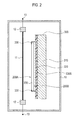
- Fig. 1 is a schematic diagram showing a configuration of a catalytic CVD equipment 100.
- the catalytic CVD equipment 100 is a device that performs formation of film by supplying a raw material gas to a heated catalytic wire which is instated in a reaction chamber, and depositing generated decomposed species onto a substrate held on a holder in the reaction chamber.
- the catalytic CVD equipment 100 is provided with a reaction chamber 10, a gas supply pipe 20, and a gas exhaust pipe 30.
- the reaction chamber 10 is provided with a catalytic wire 11 and a mount portion 12.
- a holder 300 for holding a substrate 200 is housed.
- the catalytic wire 11 is heated to thereby decompose a raw material gas to be supplied into the reaction chamber 10. Both ends of the catalytic wire 11 are mounted on the mount portion 12, and are disposed perpendicular to a bottom face of the reaction chamber 10. The catalytic wire 11 is disposed so as to be opposed to a holding face whose side is to hold the substrate 200 of the holder 300. While a distance between the catalytic wire 11 and a film-formed face of the substrate 200 is appropriately set, for example, the distance is set on the order of 100 mm to 140 mm.
- the catalytic wire 11 is electrically powered to be thereby heated to a temperature to an extent such that the raw material gas can be decomposed (for example, 1,600 degrees Centigrade to 2,000 degrees Centigrade).
- the raw material gas is decomposed by means of the catalytic wire 11 and then the decomposed species reaches the top of a first main face 200A of the substrate 200, whereby a deposited film (such as a semiconductor film or a SiN film, for example) is formed on the substrate 200.
- a deposited film such as a semiconductor film or a SiN film, for example
- the catalytic wire 11 can be made of a material such as Ta, Mo, or W.
- the catalytic wire 11 may have different kinds of layers on surface.
- One example of such layer includes a tantalum wire of which a borate layer is formed on surface.
- the catalytic wire 11 whose diameter is 0.3 mm to 2.0 mm, preferably 0.5 mm to 1.0 mm, is employed.
- the mount portion 12 is made of a material having its electrical conductivity.
- a terminal 13 that is electrically connected to the mount portion 12 is connected to a power source, although not shown.
- a power source there can be employed a constant current power source, a constant voltage power source, or constant current/constant voltage power source that is capable of both of constant current control and constant power control.
- the gas supply pipe 20 communicates with the reaction chamber 10 and a gas cylinder (not shown) containing a raw material gas (such as SiH 4 and H 2 ).
- the gas supply pipe 20 is a flow path for supplying the raw material gas into the reaction chamber 10.
- the gas exhaust pipe 30 is a flow path for discharging the raw material gas from the inside of the reaction chamber 10.
- the gas exhaust pipe 30 is capable of discharging the gas that remains in the reaction chamber 10 in order to keep the inside of the reaction chamber 10 in a vacuumed state.
- Fig. 2 is a side view of the holder 300 that is disposed in the reaction chamber 10.
- the holder 300 has a holding face 300S, a substrate portion 310, an antireflective film 320, and a holding structure 330.
- the substrate portion 310 is a substrate for holding the substrate 200 on the holding face 300S.
- the substrate 310 can be made of a metal material with its good thermal conductivity such as aluminum or stainless steel.
- the substrate 200 is a substrate on which a deposited film is to be formed.
- the substrate 200 is formed in a plate-like shape, for example, and has: a first main face 200A on which a deposited film is to be formed; and a second main face 200B that is provided at the opposite side of the first main face 200A. As shown in Fig. 2 , the second main face 200B of the substrate 200 is opposed to the holding face 300S.
- a concave-convex structure is formed on the holding face 300S.
- the size of the concave-convex structure is on the order of 2 microns to 5 microns in height and on the order of 2 microns to 5 microns in pitches, for example.
- Such a concave-convex structure can be formed by applying blast treatment to the holding face 300S, for example.
- the concave-convex structure may be formed in a substantially full area of the holding face 300S, it is preferable that the structure be formed in at least an area that is opposite to the second main face 200B of the substrate 200 of the holding face 300S.
- the holding structure 330 is mounted on the substrate portion 310. It is sufficient if the holding structure 330 hold the substrate 200 on the holding face 300S, for example, a configuration of a substrate press mask and a mask mount member can be employed. The holding structure 330 may be detachable from the substrate portion 310.
- the antireflective film 320 is formed on the holding face 300S.
- the antireflective film 320 covers a concave-convex structure that is formed on the holding face 300S.
- the antireflective film 320 reduces reflection of a radiant ray toward the side of the substrate 200 due to the substrate portion 310 by performing absorption or the like of the radiant ray that is ejected from the catalytic wire 11 and then passes through the substrate 200 (such as an infrared ray or a visible ray, for example).
- the antireflective film 320 can be made of a silicon-containing film that contains silicon. According to such a silicon-containing film, a radiant ray permeating through the substrate 200 can be absorbed, thus making it possible to reduce reflection of the radiant ray toward the side of the substrate 200 by means of the substrate portion 310.
- Fig. 3 is a view showing a reflective index of a sample 1 that is fabricated by forming an amorphous silicon film with its thickness of 3 microns on an aluminum film with its thickness of 250 nm, the aluminum film being formed on a glass substrate, by employing a plasma CVD technique.
- Fig. 4 is a view showing a reflective index of a sample 2 fabricated by forming an amorphous silicon film with its thickness of 50 microns on an aluminum film with its thickness of 250 nm, the aluminum film being formed on a glass substrate, by employing a plasma CVD technique.
- Fig. 3 is a view showing a reflective index of a sample 1 that is fabricated by forming an amorphous silicon film with its thickness of 3 microns on an aluminum film with its thickness of 250 nm, the aluminum film being formed on a glass substrate, by employing a plasma CVD technique.
- FIG. 5 is a view showing a reflective index of a sample 3 without an amorphous silicon film, the sample being fabricated by forming an aluminum film with its thickness of 250 nm on a glass substrate. From these figures, it is found that the reflective index of each of the samples 1 and 2 with an amorphous silicon film is smaller than that of the sample 3 without an amorphous silicon film.
- a silicon-containing film there can be employed a film substantially entirely containing an amorphous structure as seen in amorphous silicon film or a film partially containing a crystalline structure as seen in finely crystalline silicon film.
- the silicon-containing film may substantially entirely contain a crystalline structure.
- a material of silicon-containing film there can be employed the one containing a silicon alloy such as silicon germanium or silicon carbide without being limitative to silicon.
- a silicon-containing film may or may not contain impurities for valence electron control.
- the abovementioned catalytic CVD equipment 100 can be employed; and therefore, the catalytic CVD technique is preferable in particular. It is sufficient if the antireflective film 320 have a thickness of about 1.5 microns to 3 microns, for example.
- the antireflective film 320 can be formed by employing a mixed crystal film such as alumina, titania, and chrome oxide.
- a mixed crystal film such as alumina, titania, and chrome oxide.
- the radiant ray that permeates through the substrate 200 is scattered on a crystalline interface, thus making it possible to change an incident angle of the radiant ray to the antireflective film 320. Therefore, the radiant ray that permeates through the substrate 200 can be confined in the antireflective film 320, thus making it possible to reduce reflection of the radiant ray toward the side of the substrate 200.
- such mixed crystal film can be fabricated by means of a variety of methods such as vapor deposition technique, plasma thermal spraying technique or reactive sputtering technique.
- a mixed crystal film of alumina can be formed.
- oxygen is employed as an activation gas
- a plasma jet with its high temperature and high speed exceeding 10,000 degrees Centigrade is generated between an anode and a cathode by means of direct current arc discharge
- aluminum powder is entered into the plasma jet, melting and acceleration is performed, and a film is formed, whereby a mixed crystal film of alumina can be formed.
- the reactive sputtering technique oxygen is introduced at the time of sputtering employing an aluminum target, whereby a mixed crystal film of alumina can be formed. Further, by employing such a mixed crystal film, even in a case of employing the holder 300 on which an amorphous silicon film cannot be formed, the antireflective film 320 can be formed on the holding face 300S.
- the antireflective film 320 may be formed in a substantially full area of the holding face 300S, it is preferable that the film be formed in at least an area that is opposite to the second main face 200B of the holding face 300S.
- the antireflective film 320 that is formed on the holding face 300S is provided as one example of an “antireflective structure” according to the present invention.
- the "antireflective structure” used here denotes a structure for preventing reflection toward the side of the substrate 200 by means of the substrate portion 310 of the radiant ray that is ejected from the catalytic wire 11 and permeates through the substrate 200.
- the holder 300 has the antireflective film 320 as an antireflective structure for preventing reflection toward the side of the substrate 200 by means of the substrate portion 310 of the radiant ray that is ejected from the catalytic wire 11.
- a deposited film is formed on the first main face 200A of the substrate 200
- reflection of the radiant ray such as an infrared ray or a visible ray, for example
- part of the energy of the radiant ray is transmitted as a heat to the substrate portion 310 with its good thermal conductivity.
- the substrate 200 is restrained from being overheated, and a temperature of the substrate 200 is easily controlled in a preferred temperature range, thus making it possible to form a deposited film having its good film quality.
- a deposited film is formed by employing such a holder 300, thereby making it possible to obtain its good film property.
- the antireflective structure has a concave-convex structure that is formed on the holding face 300S.
- an optical path length in the antireflective film 320 of the radiant ray that is reflected on the holding face 300S can be increased, thus making it possible to absorb or confine the radiant ray more effectively.
- overheat of the substrate 200 can be restrained more significantly.
- adhesion between the holding face 300S and the antireflective film 320 can be improved, thus making it possible to restrain release of the antireflective film 320 from the holding face 3005.
- a concave-convex structure was formed on the holding face 300S, such concavities and convexities may not be formed. That is, as shown in Fig. 6 , there may be employed a holder 400 in which an antireflective film 420 is formed on a flat holding face 400S of a substrate portion 410.
- the antireflective structure of the holder 300 was formed by means of the antireflective film 320 this structure is not limitative thereto.
- the holder 300 may be a structure having an opening that is formed in an area that is opposite to the second main face 200B, that is, in an area that is opposite to the catalytic wire 11 while the substrate 200 is sandwiched therebetween.
- the radiant ray that is ejected from the catalytic wire 11 and permeates through the substrate 200 passes through an opening of the holder 300; and therefore, the radiant ray that is reflected by means of the holder 300 can be reduced.
- the antireflective structure was formed integrally with the holder 300, this structure is not limitative thereto.
- the antireflective structure may be a structure that is formed independently of the holder 300, and this structure may be mounted to the holder 300.
- the catalytic CVD equipment 100 and the holder 300 can be employed to form a film other than a semiconductor film such as an amorphous Si film or a semiconductor film such as a SiN film.
- the catalytic CVD equipment 100 and the holder 300 can be employed in a process of production of semiconductor devices such as solar cells that are provided with at least one of a semiconductor film and another non-semiconductor film.
- the substrate 200 is restrained from being overheated, and a temperature of the substrate 200 can be controlled in a preferred temperature range, thus making it possible to produce a film or a solar cell having its good property.
- the catalytic CVD equipment 100 was arranged so as to be provided with only one reaction chamber 10, this device is not limitative thereto.
- the catalytic CVD equipment 100 may be provided with a plurality of reaction chambers. In this manner, films of a same kind or films of different kinds can be formed to be superimposed on the substrate 200.
- an aluminum plate was prepared, the plate having a flat holding face and an amorphous silicon layer with its thickness of about 2 microns, the layer being formed on the holding face by means of a catalytic CVD technique.
- an aluminum plate was prepared, the plate having a holding face on which a concave-convex structure is formed and an amorphous silicon layer with its thickness of about 2 microns, the layer being formed on the holding face by means of the catalytic CVD technique, was prepared.
- an aluminum plate was prepared, the plate having a flat holding face and an amorphous silicon layer with its thickness of about 1 micron, the layer being formed on the holding face by means of a catalytic CVD technique, was prepared.
- silicon plates were held as substrates on the respective holders in Example 1 and Comparative Example.
- each of the holders was transported into a reaction chamber in which a catalytic wire was arranged, and the substrate and the catalytic wire were disposed so as to be opposed to each other.
- the catalytic wire was heated up to the order of 1,600 degrees Centigrade to 2,000 degrees Centigrade, and thereafter, in this state, the heated catalytic wire was left as is, for 300 seconds.
- the measured surface temperature of the substrate that was held on the holder of Example 1 was 300 degrees Centigrade, whereas the measured surface temperature of the substrate that was held on the holder of Comparative Example was about 400 degrees Centigrade.
- each of the holders was transported in a reaction chamber in which a catalytic wire was arranged, and the substrate and the catalytic wire were disposed so as to be opposed to each other.
- Fig. 7 is a graph depicting a change in each of the surface temperatures of the substrates that are held on the holders in Example 2, Example 3, and Comparative Example.
- Example 2 the surface temperature of the substrate that was held on the holder in Example 2 is gently increased in comparison with the surface temperature of the substrate that was held on the holder in Example 3.
- Example 2 has an amorphous silicon layer with its greater thickness in comparison with that of the holder in Example 3, and that a concave-convex structure is formed on a holding face, whereby reflection of the radiant ray ejected from the catalytic wire on the holding face could be restrained more effectively.
- overheat of the substrate temperature can be restrained according to the present invention; and therefore, it was found that the substrate temperature can be controlled in an appropriate temperature range.
- a deposited film with its good film quality and a solar cell with its good solar cell property can be produced by employing the present invention.
- a catalytic CVD equipment is capable of restraining overheating of a substrate, and is capable of controlling a temperature of the substrate in a preferred temperature range; and therefore, this device is useful in the field of forming a film such as the field of production of solar cell.
- a method for formation of film and a process for production of solar cell are capable of providing a deposited film with its good film quality and a solar cell with its good solar cell property; and therefore, the method and process are useful in the field of production of solar cell.
- a substrate holder according to the present invention is useful in the field of production of solar cell, since overheat of the substrate is restrained.
Landscapes
- Chemical & Material Sciences (AREA)
- General Chemical & Material Sciences (AREA)
- Chemical Kinetics & Catalysis (AREA)
- Engineering & Computer Science (AREA)
- Materials Engineering (AREA)
- Mechanical Engineering (AREA)
- Metallurgy (AREA)
- Organic Chemistry (AREA)
- Inorganic Chemistry (AREA)
- Health & Medical Sciences (AREA)
- Toxicology (AREA)
- Chemical Vapour Deposition (AREA)
Abstract
Description
- The present invention relates to a catalytic CVD equipment which is employed in a catalytic CVD technique, a method for formation of film, a process for production of solar cell, and a substrate holder.
- As a method for forming a predetermined deposited film on a substrate at the time of producing a variety of semiconductor devices such as solar cells, in general, a CVD technique (a Chemical Vapor Deposition technique) is conventionally known. As one kind of such CVD technique, in recent years, a catalytic CVD technique utilizing Catalytic Chemical Vapor Deposition has been discussed (Patent Document 1, for example).
- In the catalytic CVD technique, a raw material gas to be supplied into a reaction chamber is decomposed by employing a catalytic wire that is made of heated tungsten, molybdenum or the like and then a deposited film is formed on a substrate that is held on a holder. The catalytic CVD technique is expected as a method for formation of film, by which a substrate surface or a deposited film surface is less adversely affected, since such plasma discharge in a plasma CVD technique is not utilized.
- Patent Document 1: Japanese Unexamined Patent Application Publication No.
2005-327995 - In the abovementioned catalytic CVD technique, a catalytic wire is heated up to the order of about 1,600 degrees Centigrade to 2,000 degrees Centigrade. In this duration, a radiant ray (such as an infrared ray or a visible ray, for example) is ejected from the catalytic wire, and a substrate absorbs the radiant ray by itself, and is thereby heated.
- At this time, the substrate is easily overheated up to a temperature which is higher than a preferred temperature to form a quality film by absorbing the radiant ray that passes through the substrate and then is reflected by means of the holder. If a film is deposited on the substrate in such a state, the film quality of the deposited film may be degraded. In addition, such a problem does not occur with only a semiconductor device, but can generally occur in a case where a deposited film is formed by means of the catalytic CVD technique.
- The present invention has been made in view of the above-described circumstance, and it is an object of the present invention to provide a catalytic CVD equipment, a method for formation of film, a process for production of solar cell, and a substrate holder that are capable of restraining overheating of a substrate.
- A catalytic CVD equipment according to the present invention, is summarized as a catalytic CVD equipment for performing formation of film by supplying a raw material gas to a catalytic wire that is installed and heated in a reaction chamber and then depositing generated decomposed species on a substrate that is held on a holder in the reaction chamber, the holder including an antireflective structure for preventing reflection of a radiant ray that is ejected from the catalytic wire.
- In a catalytic CVD equipment according to the present invention, the antireflective structure may include an antireflective film.
- In a catalytic CVD equipment according to the present invention, the antireflective film may include a silicon-containing film.
- In a catalytic CVD equipment according to the present invention, the silicon-containing film may have at least one structure of an amorphous structure and a crystalline structure.
- In a catalytic CVD equipment according to the present invention, the antireflective film may include a mixed crystal film.
- In a catalytic CVD equipment according to the present invention, the antireflective structure may have a concave-convex structure that is provided so as to be opposed to the substrate.
- A catalytic CVD equipment according to the present invention is summarized as a catalytic CVD equipment for performing formation of film by supplying a raw material gas to a catalytic wire that is instated and heated in a reaction chamber and then depositing generated decomposed species on a substrate that is held on a holder in the reaction chamber, the holder including a silicon-containing film that is formed on a holding face for holding the substrate.
- A method of formation of a film according to the present invention is summarized as a method of formation of a film, said method including the step of depositing a film on a substrate to perform formation of film, wherein formation of film of the film is performed by employing the catalytic CVD equipment according to the foregoing present invention.
- A process for production of a solar cell according to the present invention is summarized as a process for production of a solar cell, said process including the step of depositing a film on a substrate to perform formation of film, wherein formation of film of the film is performed by employing the catalytic CVD equipment according to the foregoing present invention.
- A substrate holder according to the present invention is summarized as a substrate holder for performing formation of film by supplying a raw material gas to a catalytic wire that is installed and heated in a reaction chamber and then depositing generated decomposed species on a substrate that is held on a holder in the reaction chamber, the holder including an antireflective structure for preventing reflection of a radiant ray that is ejected from the catalytic wire.
- According to the present invention, there can be provided a catalytic CVD equipment that is capable of restraining overheating of a substrate and easily controlling a temperature of the substrate in a preferred temperature range. In addition, there can be provided a method for formation of film and a process for production of solar cell, which are capable of providing a deposited film with its good film quality and solar cell with its good solar cell property, by employing the catalytic CVD equipment. Further, there can be provided a substrate holder that is capable of restraining overheating of a substrate in a case where the holder is employed in the catalytic CVD equipment.
-
- [
Fig. 1] Fig. 1 is a schematic diagram showing a configuration of acatalytic CVD equipment 100 according to an embodiment. - [
Fig. 2] Fig. 2 is a schematic diagram showing a configuration of aholder 300 according to the embodiment. - [
Fig. 3] Fig. 3 is a view showing a reflective index of a sample 1 according to the embodiment. - [
Fig. 4] Fig. 4 is a view showing a reflective index of asample 2 according to the embodiment. - [
Fig. 5] Fig. 5 is a view showing a reflective index of a sample 3according to the embodiment. - [
Fig. 6] Fig. 6 is a schematic diagram showing a configuration of aholder 400 according to the embodiment. - [
Fig. 7] Fig. 7 is a graph depicting a change of each of the surface temperatures of substrates that are held on holders of Example 2, Example 3, and Comparative Example. - Hereinafter, a catalytic CVD equipment according to an embodiment of the present invention will be described with reference to the drawings. It is to be noted that, in the following description of drawings, the same or similar constituent elements are designated by the same or similar reference numerals.
- However, it should be kept in mind that the drawings are schematic, and a rate of each dimension is different from actual one. Therefore, specific dimensions or the like should be determined in consideration of the following description. In addition, it is a matter of course that portions with their different dimensional interrelationships or rates are included in the drawings.
- Hereinafter, a configuration of a catalytic CVD equipment employed in the embodiment will be described with reference to the drawings.
Fig. 1 is a schematic diagram showing a configuration of acatalytic CVD equipment 100. Thecatalytic CVD equipment 100 is a device that performs formation of film by supplying a raw material gas to a heated catalytic wire which is instated in a reaction chamber, and depositing generated decomposed species onto a substrate held on a holder in the reaction chamber. As shown inFig. 1 , thecatalytic CVD equipment 100 is provided with areaction chamber 10, agas supply pipe 20, and agas exhaust pipe 30. - The
reaction chamber 10 is provided with acatalytic wire 11 and amount portion 12. In thereaction chamber 10, aholder 300 for holding asubstrate 200 is housed. - The
catalytic wire 11 is heated to thereby decompose a raw material gas to be supplied into thereaction chamber 10. Both ends of thecatalytic wire 11 are mounted on themount portion 12, and are disposed perpendicular to a bottom face of thereaction chamber 10. Thecatalytic wire 11 is disposed so as to be opposed to a holding face whose side is to hold thesubstrate 200 of theholder 300. While a distance between thecatalytic wire 11 and a film-formed face of thesubstrate 200 is appropriately set, for example, the distance is set on the order of 100 mm to 140 mm. Thecatalytic wire 11 is electrically powered to be thereby heated to a temperature to an extent such that the raw material gas can be decomposed (for example, 1,600 degrees Centigrade to 2,000 degrees Centigrade). The raw material gas is decomposed by means of thecatalytic wire 11 and then the decomposed species reaches the top of a firstmain face 200A of thesubstrate 200, whereby a deposited film (such as a semiconductor film or a SiN film, for example) is formed on thesubstrate 200. - The
catalytic wire 11 can be made of a material such as Ta, Mo, or W. In addition, thecatalytic wire 11 may have different kinds of layers on surface. One example of such layer includes a tantalum wire of which a borate layer is formed on surface. Further, thecatalytic wire 11 whose diameter is 0.3 mm to 2.0 mm, preferably 0.5 mm to 1.0 mm, is employed. - The
mount portion 12 is made of a material having its electrical conductivity. Aterminal 13 that is electrically connected to themount portion 12 is connected to a power source, although not shown. As a power source, there can be employed a constant current power source, a constant voltage power source, or constant current/constant voltage power source that is capable of both of constant current control and constant power control. - The
gas supply pipe 20 communicates with thereaction chamber 10 and a gas cylinder (not shown) containing a raw material gas (such as SiH4 and H2). Thegas supply pipe 20 is a flow path for supplying the raw material gas into thereaction chamber 10. - The
gas exhaust pipe 30 is a flow path for discharging the raw material gas from the inside of thereaction chamber 10. In addition, thegas exhaust pipe 30 is capable of discharging the gas that remains in thereaction chamber 10 in order to keep the inside of thereaction chamber 10 in a vacuumed state. - Next, a configuration of the
holder 300 will be described with reference toFig. 2. Fig. 2 is a side view of theholder 300 that is disposed in thereaction chamber 10. - As shown in
Fig. 2 , theholder 300 has a holdingface 300S, asubstrate portion 310, anantireflective film 320, and a holdingstructure 330. - The
substrate portion 310 is a substrate for holding thesubstrate 200 on the holdingface 300S. Thesubstrate 310 can be made of a metal material with its good thermal conductivity such as aluminum or stainless steel. - The
substrate 200 is a substrate on which a deposited film is to be formed. Thesubstrate 200 is formed in a plate-like shape, for example, and has: a firstmain face 200A on which a deposited film is to be formed; and a secondmain face 200B that is provided at the opposite side of the firstmain face 200A. As shown inFig. 2 , the secondmain face 200B of thesubstrate 200 is opposed to the holdingface 300S. - Here, a concave-convex structure is formed on the holding
face 300S. The size of the concave-convex structure is on the order of 2 microns to 5 microns in height and on the order of 2 microns to 5 microns in pitches, for example. Such a concave-convex structure can be formed by applying blast treatment to the holdingface 300S, for example. - Although the concave-convex structure may be formed in a substantially full area of the holding
face 300S, it is preferable that the structure be formed in at least an area that is opposite to the secondmain face 200B of thesubstrate 200 of the holdingface 300S. - The holding
structure 330 is mounted on thesubstrate portion 310. It is sufficient if the holdingstructure 330 hold thesubstrate 200 on the holdingface 300S, for example, a configuration of a substrate press mask and a mask mount member can be employed. The holdingstructure 330 may be detachable from thesubstrate portion 310. - The
antireflective film 320 is formed on the holdingface 300S. In the embodiment, theantireflective film 320 covers a concave-convex structure that is formed on the holdingface 300S. Theantireflective film 320 reduces reflection of a radiant ray toward the side of thesubstrate 200 due to thesubstrate portion 310 by performing absorption or the like of the radiant ray that is ejected from thecatalytic wire 11 and then passes through the substrate 200 (such as an infrared ray or a visible ray, for example). - In addition, the
antireflective film 320 can be made of a silicon-containing film that contains silicon. According to such a silicon-containing film, a radiant ray permeating through thesubstrate 200 can be absorbed, thus making it possible to reduce reflection of the radiant ray toward the side of thesubstrate 200 by means of thesubstrate portion 310. -
Fig. 3 is a view showing a reflective index of a sample 1 that is fabricated by forming an amorphous silicon film with its thickness of 3 microns on an aluminum film with its thickness of 250 nm, the aluminum film being formed on a glass substrate, by employing a plasma CVD technique.Fig. 4 is a view showing a reflective index of asample 2 fabricated by forming an amorphous silicon film with its thickness of 50 microns on an aluminum film with its thickness of 250 nm, the aluminum film being formed on a glass substrate, by employing a plasma CVD technique.Fig. 5 is a view showing a reflective index of asample 3 without an amorphous silicon film, the sample being fabricated by forming an aluminum film with its thickness of 250 nm on a glass substrate. From these figures, it is found that the reflective index of each of thesamples 1 and 2 with an amorphous silicon film is smaller than that of thesample 3 without an amorphous silicon film. - It is to be noted that, as a silicon-containing film, there can be employed a film substantially entirely containing an amorphous structure as seen in amorphous silicon film or a film partially containing a crystalline structure as seen in finely crystalline silicon film. Alternatively, the silicon-containing film may substantially entirely contain a crystalline structure. In addition, as a material of silicon-containing film, there can be employed the one containing a silicon alloy such as silicon germanium or silicon carbide without being limitative to silicon. Further, a silicon-containing film may or may not contain impurities for valence electron control. While such a silicon-containing film can be formed by means of a catalytic CVD technique, a plasma CVD technique, or a vacuum vapor deposition technique, the abovementioned
catalytic CVD equipment 100 can be employed; and therefore, the catalytic CVD technique is preferable in particular. It is sufficient if theantireflective film 320 have a thickness of about 1.5 microns to 3 microns, for example. - In addition, the
antireflective film 320 can be formed by employing a mixed crystal film such as alumina, titania, and chrome oxide. According to theantireflective film 320 employing such a mixed crystal film, the radiant ray that permeates through thesubstrate 200 is scattered on a crystalline interface, thus making it possible to change an incident angle of the radiant ray to theantireflective film 320. Therefore, the radiant ray that permeates through thesubstrate 200 can be confined in theantireflective film 320, thus making it possible to reduce reflection of the radiant ray toward the side of thesubstrate 200. It is to be noted that such mixed crystal film can be fabricated by means of a variety of methods such as vapor deposition technique, plasma thermal spraying technique or reactive sputtering technique. For example, by employing the vapor deposition technique, aluminum that is housed in melting pot is heated and evaporated in an oxygen atmosphere, whereby a mixed crystal film of alumina can be formed. In addition, by employing the plasma thermal spraying technique, oxygen is employed as an activation gas, a plasma jet with its high temperature and high speed exceeding 10,000 degrees Centigrade is generated between an anode and a cathode by means of direct current arc discharge, aluminum powder is entered into the plasma jet, melting and acceleration is performed, and a film is formed, whereby a mixed crystal film of alumina can be formed. Alternatively, by employing the reactive sputtering technique, oxygen is introduced at the time of sputtering employing an aluminum target, whereby a mixed crystal film of alumina can be formed. Further, by employing such a mixed crystal film, even in a case of employing theholder 300 on which an amorphous silicon film cannot be formed, theantireflective film 320 can be formed on the holdingface 300S. - Although the
antireflective film 320 may be formed in a substantially full area of the holdingface 300S, it is preferable that the film be formed in at least an area that is opposite to the secondmain face 200B of the holdingface 300S. - Herein, the
antireflective film 320 that is formed on the holdingface 300S is provided as one example of an "antireflective structure" according to the present invention. The "antireflective structure" used here denotes a structure for preventing reflection toward the side of thesubstrate 200 by means of thesubstrate portion 310 of the radiant ray that is ejected from thecatalytic wire 11 and permeates through thesubstrate 200. - In the
catalytic CVD equipment 100 according to the embodiment, theholder 300 has theantireflective film 320 as an antireflective structure for preventing reflection toward the side of thesubstrate 200 by means of thesubstrate portion 310 of the radiant ray that is ejected from thecatalytic wire 11. - Therefore, in a case where a deposited film is formed on the first
main face 200A of thesubstrate 200, reflection of the radiant ray (such as an infrared ray or a visible ray, for example) that is ejected from thecatalytic wire 11 and permeates through thesubstrate 200 is reduced by means of theantireflective film 320, and part of the energy of the radiant ray is transmitted as a heat to thesubstrate portion 310 with its good thermal conductivity. Thus, thesubstrate 200 is restrained from being overheated, and a temperature of thesubstrate 200 is easily controlled in a preferred temperature range, thus making it possible to form a deposited film having its good film quality. Accordingly, a deposited film is formed by employing such aholder 300, thereby making it possible to obtain its good film property. - In addition, in the embodiment, the antireflective structure has a concave-convex structure that is formed on the holding
face 300S. In this case, an optical path length in theantireflective film 320 of the radiant ray that is reflected on the holdingface 300S can be increased, thus making it possible to absorb or confine the radiant ray more effectively. As a result, overheat of thesubstrate 200 can be restrained more significantly. - Further, adhesion between the holding
face 300S and theantireflective film 320 can be improved, thus making it possible to restrain release of theantireflective film 320 from the holding face 3005. - While the present invention was described by way of the foregoing embodiment, it should not be understood that the statements and drawings forming part of this disclosure limit this invention. From this disclosure, a variety of substitute embodiments, examples, and operating techniques would have been self-evident to one skilled in the art.
- For example, while, in the foregoing embodiment, a concave-convex structure was formed on the holding
face 300S, such concavities and convexities may not be formed. That is, as shown inFig. 6 , there may be employed aholder 400 in which anantireflective film 420 is formed on aflat holding face 400S of asubstrate portion 410. - In addition, while, in the foregoing embodiment, the antireflective structure of the
holder 300 was formed by means of theantireflective film 320 this structure is not limitative thereto. For example, in the antireflective structure, theholder 300 may be a structure having an opening that is formed in an area that is opposite to the secondmain face 200B, that is, in an area that is opposite to thecatalytic wire 11 while thesubstrate 200 is sandwiched therebetween. In this case, the radiant ray that is ejected from thecatalytic wire 11 and permeates through thesubstrate 200 passes through an opening of theholder 300; and therefore, the radiant ray that is reflected by means of theholder 300 can be reduced. - Further, while, in the foregoing embodiment, the antireflective structure was formed integrally with the
holder 300, this structure is not limitative thereto. For example, the antireflective structure may be a structure that is formed independently of theholder 300, and this structure may be mounted to theholder 300. - Furthermore, although not specifically mentioned in the foregoing embodiment, the
catalytic CVD equipment 100 and theholder 300, according to the present invention, can be employed to form a film other than a semiconductor film such as an amorphous Si film or a semiconductor film such as a SiN film. Moreover, thecatalytic CVD equipment 100 and theholder 300 can be employed in a process of production of semiconductor devices such as solar cells that are provided with at least one of a semiconductor film and another non-semiconductor film. Thus, by employing thecatalytic CVD equipment 100 or theholder 300 according to the present invention, thesubstrate 200 is restrained from being overheated, and a temperature of thesubstrate 200 can be controlled in a preferred temperature range, thus making it possible to produce a film or a solar cell having its good property. - Still furthermore, while, in the foregoing embodiment, the
catalytic CVD equipment 100 was arranged so as to be provided with only onereaction chamber 10, this device is not limitative thereto. Thecatalytic CVD equipment 100 may be provided with a plurality of reaction chambers. In this manner, films of a same kind or films of different kinds can be formed to be superimposed on thesubstrate 200. - While Examples of the holder according to the present invention will be specifically described hereinafter, the present invention is not limitative to the descriptive matter set forth in the following Examples, and the present invention can be appropriately modified and carried out without departing from the spirit and scope of the invention.
- As a holder according to Example 1, an aluminum plate was prepared, the plate having a flat holding face and an amorphous silicon layer with its thickness of about 2 microns, the layer being formed on the holding face by means of a catalytic CVD technique.
- As a holder according to Example 2, an aluminum plate was prepared, the plate having a holding face on which a concave-convex structure is formed and an amorphous silicon layer with its thickness of about 2 microns, the layer being formed on the holding face by means of the catalytic CVD technique, was prepared.
- As a holder according to Example 3, an aluminum plate was prepared, the plate having a flat holding face and an amorphous silicon layer with its thickness of about 1 micron, the layer being formed on the holding face by means of a catalytic CVD technique, was prepared.
- As a holder according to Comparative Example, an aluminum plate having a flat holding face was prepared.
- First, silicon plates were held as substrates on the respective holders in Example 1 and Comparative Example.
- Next, each of the holders was transported into a reaction chamber in which a catalytic wire was arranged, and the substrate and the catalytic wire were disposed so as to be opposed to each other.
- Next, the catalytic wire was heated up to the order of 1,600 degrees Centigrade to 2,000 degrees Centigrade, and thereafter, in this state, the heated catalytic wire was left as is, for 300 seconds.
- Next, when surface temperatures of the substrates were measured, the measured surface temperature of the substrate that was held on the holder of Example 1 was 300 degrees Centigrade, whereas the measured surface temperature of the substrate that was held on the holder of Comparative Example was about 400 degrees Centigrade.
- It is deemed that a reason why such a result was obtained is that, in the holder of Example 1, reflection of the radiant ray permeating through the substrate and hitting against the holder toward the side of the substrate could be restrained by means of the antireflective structure included in the holder.
- First, silicon plates were held as substrates on the respective the holders in Example 2, Comparative Example, and Example 3.
- Next, each of the holders was transported in a reaction chamber in which a catalytic wire was arranged, and the substrate and the catalytic wire were disposed so as to be opposed to each other.
- Next, a change in the surface temperature of the substrate was measured while the catalytic wire was heated up to the order of 1,600 degrees Centigrade to 2,000 degrees Centigrade.
Fig. 7 is a graph depicting a change in each of the surface temperatures of the substrates that are held on the holders in Example 2, Example 3, and Comparative Example. - As shown in
Fig. 7 , it was found that the surface temperatures of the substrates that were held on the holders in Example 2 and Example 3 are gently increased in comparison with the surface temperature of the substrate that was held on the holder in Comparative Example. - It is deemed that a reason why such a result was obtained is that, in the holders of Example 2 and Example 3, reflection of the radiant ray that permeates through the substrate and hits against the holders toward the side of the substrate could be restrained by means of the antireflective structure included in the holders.
- In addition, it was found that the surface temperature of the substrate that was held on the holder in Example 2 is gently increased in comparison with the surface temperature of the substrate that was held on the holder in Example 3.
- It is deemed that a reason for this finding is that the holder in Example 2 has an amorphous silicon layer with its greater thickness in comparison with that of the holder in Example 3, and that a concave-convex structure is formed on a holding face, whereby reflection of the radiant ray ejected from the catalytic wire on the holding face could be restrained more effectively.
- From the foregoing, overheat of the substrate temperature can be restrained according to the present invention; and therefore, it was found that the substrate temperature can be controlled in an appropriate temperature range. In addition, it is deemed that a deposited film with its good film quality and a solar cell with its good solar cell property can be produced by employing the present invention.
- It is to be noted that the entire contents of Japanese Patent Application No.
2009-230589 (filed on October 2, 2009 - As described above, a catalytic CVD equipment according to the present invention is capable of restraining overheating of a substrate, and is capable of controlling a temperature of the substrate in a preferred temperature range; and therefore, this device is useful in the field of forming a film such as the field of production of solar cell. In addition, a method for formation of film and a process for production of solar cell, according to the present invention, are capable of providing a deposited film with its good film quality and a solar cell with its good solar cell property; and therefore, the method and process are useful in the field of production of solar cell. Further, a substrate holder according to the present invention is useful in the field of production of solar cell, since overheat of the substrate is restrained.
-
- 10...
- Reaction chamber
- 11...
- Catalytic wire
- 12...
- Mount portion
- 13...
- Terminal
- 20...
- Gas supply pipe
- 30...
- Gas exhaust pipe
- 100...
- Catalytic CVD equipment
- 200...
- Substrate
- 200A...
- First main face
- 200B...
- Second main face
- 300...
- Holder
- 3005...
- Holding face
- 310...
- Substrate portion
- 320...
- Antireflective film
- 330...
- Holding structure
- 400...
- Holder
- 4005...
- Holding face
- 410...
- Substrate portion
- 420...
- Antireflective film
Claims (10)
- A catalytic CVD equipment for performing formation of film by supplying a raw material gas to a catalytic wire that is installed and heated in a reaction chamber and then depositing generated decomposed species on a substrate that is held on a holder in the reaction chamber,
the holder including an antireflective structure for preventing reflection of a radiant ray that is ejected from the catalytic wire. - The catalytic CVD equipment according to claim 1, wherein the antireflective structure includes an antireflective film.
- The catalytic CVD equipment according to claim 2, wherein the antireflective film includes a silicon-containing film.
- The catalytic CVD equipment according to claim 3, wherein the silicon-containing film has at least one structure of an amorphous structure and a crystalline structure.
- The catalytic CVD equipment according to claim 2, wherein the antireflective film includes a mixed crystal film.
- The catalytic CVD equipment according to any one of claims 1 to 4, wherein the antireflective structure has a concave-convex structure that is provided so as to be opposed to the substrate.
- A catalytic CVD equipment for performing formation of film by supplying a raw material gas to a catalytic wire that is instated and heated in a reaction chamber and then depositing generated decomposed species on a substrate that is held on a holder in the reaction chamber,
the holder including a silicon-containing film that is formed on a holding face for holding the substrate. - A method of formation of a film, said method including the step of depositing a film on a substrate to perform formation of film, wherein formation of film of the film is performed by employing the catalytic CVD equipment according to any one of claims 1 to 6.
- A process for production of a solar cell, said process including the step of depositing a film on a substrate to perform formation of film,
wherein formation of film of the film is performed by employing the catalytic CVD equipment according to any one of claims 1 to 6. - A substrate holder for performing formation of film by supplying a raw material gas to a catalytic wire that is installed and heated in a reaction chamber and then depositing generated decomposed species on a substrate that is held on a holder in the reaction chamber,
the holder including an antireflective structure for preventing reflection of a radiant ray that is ejected from the catalytic wire.
Applications Claiming Priority (2)
| Application Number | Priority Date | Filing Date | Title |
|---|---|---|---|
| JP2009230589A JP5357689B2 (en) | 2009-10-02 | 2009-10-02 | Catalytic CVD apparatus, film forming method, solar cell manufacturing method, and substrate holder |
| PCT/JP2010/067285 WO2011040610A1 (en) | 2009-10-02 | 2010-10-01 | Catalytic cvd device, method for formation of film, process for production of solar cell, and substrate holder |
Publications (3)
| Publication Number | Publication Date |
|---|---|
| EP2484804A1 true EP2484804A1 (en) | 2012-08-08 |
| EP2484804A4 EP2484804A4 (en) | 2017-03-22 |
| EP2484804B1 EP2484804B1 (en) | 2018-12-05 |
Family
ID=43826413
Family Applications (1)
| Application Number | Title | Priority Date | Filing Date |
|---|---|---|---|
| EP10820724.2A Active EP2484804B1 (en) | 2009-10-02 | 2010-10-01 | Catalytic cvd device, method for formation of film, process for production of solar cell, and substrate holder |
Country Status (6)
| Country | Link |
|---|---|
| US (1) | US8957351B2 (en) |
| EP (1) | EP2484804B1 (en) |
| JP (1) | JP5357689B2 (en) |
| KR (1) | KR101462321B1 (en) |
| CN (1) | CN102575343B (en) |
| WO (1) | WO2011040610A1 (en) |
Cited By (1)
| Publication number | Priority date | Publication date | Assignee | Title |
|---|---|---|---|---|
| WO2020018333A1 (en) * | 2018-07-17 | 2020-01-23 | Varian Semiconductor Equipment Associates, Inc. | Anti-reflective coating for transparent end effectors |
Families Citing this family (1)
| Publication number | Priority date | Publication date | Assignee | Title |
|---|---|---|---|---|
| US20120312326A1 (en) * | 2011-06-10 | 2012-12-13 | Applied Materials, Inc. | Methods for cleaning a surface of a substrate using a hot wire chemical vapor deposition (hwcvd) chamber |
Family Cites Families (10)
| Publication number | Priority date | Publication date | Assignee | Title |
|---|---|---|---|---|
| US5444217A (en) * | 1993-01-21 | 1995-08-22 | Moore Epitaxial Inc. | Rapid thermal processing apparatus for processing semiconductor wafers |
| US6120660A (en) * | 1998-02-11 | 2000-09-19 | Silicon Genesis Corporation | Removable liner design for plasma immersion ion implantation |
| JP2001156311A (en) * | 1999-11-30 | 2001-06-08 | Sharp Corp | Thin film solar cell and method of manufacturing the same |
| JP4710187B2 (en) * | 2000-08-30 | 2011-06-29 | ソニー株式会社 | Method for growing polycrystalline silicon layer and method for epitaxial growth of single crystal silicon layer |
| JP3868324B2 (en) * | 2002-04-15 | 2007-01-17 | 三菱電機株式会社 | Silicon nitride film forming method, film forming apparatus, and semiconductor device manufacturing method |
| CN100390105C (en) * | 2003-03-26 | 2008-05-28 | 圣戈本陶瓷及塑料股份有限公司 | Silicon carbide ceramic component with oxide layer |
| JP4374278B2 (en) | 2004-05-17 | 2009-12-02 | 株式会社アルバック | Catalytic CVD equipment |
| JP4970887B2 (en) * | 2006-10-06 | 2012-07-11 | 株式会社アルバック | Method for recycling equipment components |
| JP4856010B2 (en) * | 2007-06-04 | 2012-01-18 | 株式会社アルバック | Catalytic chemical vapor deposition system |
| JP4597205B2 (en) | 2008-03-24 | 2010-12-15 | シャープ株式会社 | Printing system |
-
2009
- 2009-10-02 JP JP2009230589A patent/JP5357689B2/en active Active
-
2010
- 2010-10-01 EP EP10820724.2A patent/EP2484804B1/en active Active
- 2010-10-01 KR KR1020127011213A patent/KR101462321B1/en active Active
- 2010-10-01 CN CN201080044569.8A patent/CN102575343B/en active Active
- 2010-10-01 WO PCT/JP2010/067285 patent/WO2011040610A1/en not_active Ceased
-
2012
- 2012-03-30 US US13/435,646 patent/US8957351B2/en active Active
Non-Patent Citations (1)
| Title |
|---|
| See references of WO2011040610A1 * |
Cited By (2)
| Publication number | Priority date | Publication date | Assignee | Title |
|---|---|---|---|---|
| WO2020018333A1 (en) * | 2018-07-17 | 2020-01-23 | Varian Semiconductor Equipment Associates, Inc. | Anti-reflective coating for transparent end effectors |
| US10669430B2 (en) | 2018-07-17 | 2020-06-02 | Varian Semiconductor Equipment Associates, Inc. | Anti-reflective coating for transparent end effectors |
Also Published As
| Publication number | Publication date |
|---|---|
| WO2011040610A1 (en) | 2011-04-07 |
| KR20120073318A (en) | 2012-07-04 |
| CN102575343B (en) | 2014-04-16 |
| JP5357689B2 (en) | 2013-12-04 |
| EP2484804A4 (en) | 2017-03-22 |
| CN102575343A (en) | 2012-07-11 |
| JP2011080095A (en) | 2011-04-21 |
| US8957351B2 (en) | 2015-02-17 |
| KR101462321B1 (en) | 2014-11-14 |
| US20120190149A1 (en) | 2012-07-26 |
| EP2484804B1 (en) | 2018-12-05 |
Similar Documents
| Publication | Publication Date | Title |
|---|---|---|
| KR100907165B1 (en) | P-type semiconductor zinc oxide films process for preparation thereof, and pulsed laser deposition method using transparent substrates | |
| KR20100029126A (en) | Reactive flow deposition and synthesis of inorganic foils | |
| TWI804809B (en) | Method for bonding substrates | |
| WO2008013942A2 (en) | Methods and systems for manufacturing polycrystalline silicon and silicon-germanium solar cells | |
| US8765036B2 (en) | Method of producing a semiconductor | |
| US20090208725A1 (en) | Layer transfer for large area inorganic foils | |
| US8957351B2 (en) | Catalytic CVD equipment, method for formation of film, process for production of solar cell, and substrate holder | |
| Ohdaira et al. | Formation of several-micrometer-thick polycrystalline silicon films on soda lime glass by flash lamp annealing | |
| US20140026815A1 (en) | Separating Device and Method for Producing A Crucible For Said Separating Device | |
| TW200824140A (en) | Methods and systems for manufacturing polycrystalline silicon and silicon-germanium solar cells | |
| JP2015030918A (en) | Coating device, and method for manufacturing coating device | |
| US9620664B2 (en) | Coating of graphite tooling for manufacture of semiconductors | |
| Tveryanovich et al. | Production of nanodispersed materials and thin films by laser ablation techniques in liquid and in vacuum | |
| Bobela et al. | Epitaxial crystal silicon absorber layers and solar cells grown at 1.8 microns per minute | |
| Gromball et al. | High rate deposition and in situ doping of silicon films for solar cells on glass | |
| JP2009088029A (en) | Manufacturing method of solar cell | |
| JPH0716451A (en) | Method for producing ultrafine particle dispersed material | |
| US8658246B2 (en) | Manufacturing method of group of whiskers | |
| WO2010141045A1 (en) | Process for synthesizing a thin film or composition layer via non-contact pressure containment | |
| Heemeier et al. | Thin film technology for electron beam crystallized silicon solar cells on low cost substrates | |
| JPH06208960A (en) | Manufacture of silicon lamination body | |
| Ito et al. | Purification of Silicon Thin Films Containing Nitrogen and Oxygen Impurities using Aluminum-Induced Crystallization | |
| JP2002141530A (en) | Method for forming photovoltaic element, photovoltaic element, semiconductor element, and liquid phase growth method |
Legal Events
| Date | Code | Title | Description |
|---|---|---|---|
| PUAI | Public reference made under article 153(3) epc to a published international application that has entered the european phase |
Free format text: ORIGINAL CODE: 0009012 |
|
| 17P | Request for examination filed |
Effective date: 20120330 |
|
| AK | Designated contracting states |
Kind code of ref document: A1 Designated state(s): AL AT BE BG CH CY CZ DE DK EE ES FI FR GB GR HR HU IE IS IT LI LT LU LV MC MK MT NL NO PL PT RO RS SE SI SK SM TR |
|
| DAX | Request for extension of the european patent (deleted) | ||
| RA4 | Supplementary search report drawn up and despatched (corrected) |
Effective date: 20170220 |
|
| RIC1 | Information provided on ipc code assigned before grant |
Ipc: H01L 21/205 20060101ALI20170214BHEP Ipc: C23C 16/24 20060101ALI20170214BHEP Ipc: C23C 16/48 20060101ALI20170214BHEP Ipc: H01L 21/687 20060101ALI20170214BHEP Ipc: C23C 16/34 20060101ALI20170214BHEP Ipc: C23C 16/44 20060101AFI20170214BHEP Ipc: C23C 16/32 20060101ALI20170214BHEP |
|
| GRAP | Despatch of communication of intention to grant a patent |
Free format text: ORIGINAL CODE: EPIDOSNIGR1 |
|
| STAA | Information on the status of an ep patent application or granted ep patent |
Free format text: STATUS: GRANT OF PATENT IS INTENDED |
|
| INTG | Intention to grant announced |
Effective date: 20180704 |
|
| GRAS | Grant fee paid |
Free format text: ORIGINAL CODE: EPIDOSNIGR3 |
|
| GRAA | (expected) grant |
Free format text: ORIGINAL CODE: 0009210 |
|
| GRAA | (expected) grant |
Free format text: ORIGINAL CODE: 0009210 |
|
| STAA | Information on the status of an ep patent application or granted ep patent |
Free format text: STATUS: THE PATENT HAS BEEN GRANTED |
|
| AK | Designated contracting states |
Kind code of ref document: B1 Designated state(s): AL AT BE BG CH CY CZ DE DK EE ES FI FR GB GR HR HU IE IS IT LI LT LU LV MC MK MT NL NO PL PT RO RS SE SI SK SM TR |
|
| REG | Reference to a national code |
Ref country code: GB Ref legal event code: FG4D |
|
| REG | Reference to a national code |
Ref country code: CH Ref legal event code: EP |
|
| REG | Reference to a national code |
Ref country code: AT Ref legal event code: REF Ref document number: 1073167 Country of ref document: AT Kind code of ref document: T Effective date: 20181215 |
|
| REG | Reference to a national code |
Ref country code: IE Ref legal event code: FG4D |
|
| REG | Reference to a national code |
Ref country code: DE Ref legal event code: R096 Ref document number: 602010055668 Country of ref document: DE |
|
| REG | Reference to a national code |
Ref country code: NL Ref legal event code: MP Effective date: 20181205 |
|
| REG | Reference to a national code |
Ref country code: AT Ref legal event code: MK05 Ref document number: 1073167 Country of ref document: AT Kind code of ref document: T Effective date: 20181205 |
|
| REG | Reference to a national code |
Ref country code: LT Ref legal event code: MG4D |
|
| PG25 | Lapsed in a contracting state [announced via postgrant information from national office to epo] |
Ref country code: ES Free format text: LAPSE BECAUSE OF FAILURE TO SUBMIT A TRANSLATION OF THE DESCRIPTION OR TO PAY THE FEE WITHIN THE PRESCRIBED TIME-LIMIT Effective date: 20181205 Ref country code: AT Free format text: LAPSE BECAUSE OF FAILURE TO SUBMIT A TRANSLATION OF THE DESCRIPTION OR TO PAY THE FEE WITHIN THE PRESCRIBED TIME-LIMIT Effective date: 20181205 Ref country code: LT Free format text: LAPSE BECAUSE OF FAILURE TO SUBMIT A TRANSLATION OF THE DESCRIPTION OR TO PAY THE FEE WITHIN THE PRESCRIBED TIME-LIMIT Effective date: 20181205 Ref country code: NO Free format text: LAPSE BECAUSE OF FAILURE TO SUBMIT A TRANSLATION OF THE DESCRIPTION OR TO PAY THE FEE WITHIN THE PRESCRIBED TIME-LIMIT Effective date: 20190305 Ref country code: FI Free format text: LAPSE BECAUSE OF FAILURE TO SUBMIT A TRANSLATION OF THE DESCRIPTION OR TO PAY THE FEE WITHIN THE PRESCRIBED TIME-LIMIT Effective date: 20181205 Ref country code: BG Free format text: LAPSE BECAUSE OF FAILURE TO SUBMIT A TRANSLATION OF THE DESCRIPTION OR TO PAY THE FEE WITHIN THE PRESCRIBED TIME-LIMIT Effective date: 20190305 Ref country code: HR Free format text: LAPSE BECAUSE OF FAILURE TO SUBMIT A TRANSLATION OF THE DESCRIPTION OR TO PAY THE FEE WITHIN THE PRESCRIBED TIME-LIMIT Effective date: 20181205 Ref country code: LV Free format text: LAPSE BECAUSE OF FAILURE TO SUBMIT A TRANSLATION OF THE DESCRIPTION OR TO PAY THE FEE WITHIN THE PRESCRIBED TIME-LIMIT Effective date: 20181205 |
|
| PG25 | Lapsed in a contracting state [announced via postgrant information from national office to epo] |
Ref country code: RS Free format text: LAPSE BECAUSE OF FAILURE TO SUBMIT A TRANSLATION OF THE DESCRIPTION OR TO PAY THE FEE WITHIN THE PRESCRIBED TIME-LIMIT Effective date: 20181205 Ref country code: AL Free format text: LAPSE BECAUSE OF FAILURE TO SUBMIT A TRANSLATION OF THE DESCRIPTION OR TO PAY THE FEE WITHIN THE PRESCRIBED TIME-LIMIT Effective date: 20181205 Ref country code: SE Free format text: LAPSE BECAUSE OF FAILURE TO SUBMIT A TRANSLATION OF THE DESCRIPTION OR TO PAY THE FEE WITHIN THE PRESCRIBED TIME-LIMIT Effective date: 20181205 Ref country code: GR Free format text: LAPSE BECAUSE OF FAILURE TO SUBMIT A TRANSLATION OF THE DESCRIPTION OR TO PAY THE FEE WITHIN THE PRESCRIBED TIME-LIMIT Effective date: 20190306 |
|
| PG25 | Lapsed in a contracting state [announced via postgrant information from national office to epo] |
Ref country code: NL Free format text: LAPSE BECAUSE OF FAILURE TO SUBMIT A TRANSLATION OF THE DESCRIPTION OR TO PAY THE FEE WITHIN THE PRESCRIBED TIME-LIMIT Effective date: 20181205 |
|
| PG25 | Lapsed in a contracting state [announced via postgrant information from national office to epo] |
Ref country code: PL Free format text: LAPSE BECAUSE OF FAILURE TO SUBMIT A TRANSLATION OF THE DESCRIPTION OR TO PAY THE FEE WITHIN THE PRESCRIBED TIME-LIMIT Effective date: 20181205 Ref country code: IT Free format text: LAPSE BECAUSE OF FAILURE TO SUBMIT A TRANSLATION OF THE DESCRIPTION OR TO PAY THE FEE WITHIN THE PRESCRIBED TIME-LIMIT Effective date: 20181205 Ref country code: CZ Free format text: LAPSE BECAUSE OF FAILURE TO SUBMIT A TRANSLATION OF THE DESCRIPTION OR TO PAY THE FEE WITHIN THE PRESCRIBED TIME-LIMIT Effective date: 20181205 Ref country code: PT Free format text: LAPSE BECAUSE OF FAILURE TO SUBMIT A TRANSLATION OF THE DESCRIPTION OR TO PAY THE FEE WITHIN THE PRESCRIBED TIME-LIMIT Effective date: 20190405 |
|
| PG25 | Lapsed in a contracting state [announced via postgrant information from national office to epo] |
Ref country code: SK Free format text: LAPSE BECAUSE OF FAILURE TO SUBMIT A TRANSLATION OF THE DESCRIPTION OR TO PAY THE FEE WITHIN THE PRESCRIBED TIME-LIMIT Effective date: 20181205 Ref country code: SM Free format text: LAPSE BECAUSE OF FAILURE TO SUBMIT A TRANSLATION OF THE DESCRIPTION OR TO PAY THE FEE WITHIN THE PRESCRIBED TIME-LIMIT Effective date: 20181205 Ref country code: EE Free format text: LAPSE BECAUSE OF FAILURE TO SUBMIT A TRANSLATION OF THE DESCRIPTION OR TO PAY THE FEE WITHIN THE PRESCRIBED TIME-LIMIT Effective date: 20181205 Ref country code: RO Free format text: LAPSE BECAUSE OF FAILURE TO SUBMIT A TRANSLATION OF THE DESCRIPTION OR TO PAY THE FEE WITHIN THE PRESCRIBED TIME-LIMIT Effective date: 20181205 Ref country code: IS Free format text: LAPSE BECAUSE OF FAILURE TO SUBMIT A TRANSLATION OF THE DESCRIPTION OR TO PAY THE FEE WITHIN THE PRESCRIBED TIME-LIMIT Effective date: 20190405 |
|
| REG | Reference to a national code |
Ref country code: DE Ref legal event code: R097 Ref document number: 602010055668 Country of ref document: DE |
|
| PLBE | No opposition filed within time limit |
Free format text: ORIGINAL CODE: 0009261 |
|
| STAA | Information on the status of an ep patent application or granted ep patent |
Free format text: STATUS: NO OPPOSITION FILED WITHIN TIME LIMIT |
|
| PG25 | Lapsed in a contracting state [announced via postgrant information from national office to epo] |
Ref country code: SI Free format text: LAPSE BECAUSE OF FAILURE TO SUBMIT A TRANSLATION OF THE DESCRIPTION OR TO PAY THE FEE WITHIN THE PRESCRIBED TIME-LIMIT Effective date: 20181205 Ref country code: DK Free format text: LAPSE BECAUSE OF FAILURE TO SUBMIT A TRANSLATION OF THE DESCRIPTION OR TO PAY THE FEE WITHIN THE PRESCRIBED TIME-LIMIT Effective date: 20181205 |
|
| 26N | No opposition filed |
Effective date: 20190906 |
|
| PG25 | Lapsed in a contracting state [announced via postgrant information from national office to epo] |
Ref country code: TR Free format text: LAPSE BECAUSE OF FAILURE TO SUBMIT A TRANSLATION OF THE DESCRIPTION OR TO PAY THE FEE WITHIN THE PRESCRIBED TIME-LIMIT Effective date: 20181205 |
|
| PG25 | Lapsed in a contracting state [announced via postgrant information from national office to epo] |
Ref country code: MC Free format text: LAPSE BECAUSE OF FAILURE TO SUBMIT A TRANSLATION OF THE DESCRIPTION OR TO PAY THE FEE WITHIN THE PRESCRIBED TIME-LIMIT Effective date: 20181205 |
|
| REG | Reference to a national code |
Ref country code: CH Ref legal event code: PL |
|
| PG25 | Lapsed in a contracting state [announced via postgrant information from national office to epo] |
Ref country code: LI Free format text: LAPSE BECAUSE OF NON-PAYMENT OF DUE FEES Effective date: 20191031 Ref country code: LU Free format text: LAPSE BECAUSE OF NON-PAYMENT OF DUE FEES Effective date: 20191001 Ref country code: CH Free format text: LAPSE BECAUSE OF NON-PAYMENT OF DUE FEES Effective date: 20191031 |
|
| REG | Reference to a national code |
Ref country code: BE Ref legal event code: MM Effective date: 20191031 |
|
| PG25 | Lapsed in a contracting state [announced via postgrant information from national office to epo] |
Ref country code: BE Free format text: LAPSE BECAUSE OF NON-PAYMENT OF DUE FEES Effective date: 20191031 |
|
| GBPC | Gb: european patent ceased through non-payment of renewal fee |
Effective date: 20191001 |
|
| PG25 | Lapsed in a contracting state [announced via postgrant information from national office to epo] |
Ref country code: IE Free format text: LAPSE BECAUSE OF NON-PAYMENT OF DUE FEES Effective date: 20191001 Ref country code: GB Free format text: LAPSE BECAUSE OF NON-PAYMENT OF DUE FEES Effective date: 20191001 Ref country code: FR Free format text: LAPSE BECAUSE OF NON-PAYMENT OF DUE FEES Effective date: 20191031 |
|
| PG25 | Lapsed in a contracting state [announced via postgrant information from national office to epo] |
Ref country code: CY Free format text: LAPSE BECAUSE OF FAILURE TO SUBMIT A TRANSLATION OF THE DESCRIPTION OR TO PAY THE FEE WITHIN THE PRESCRIBED TIME-LIMIT Effective date: 20181205 |
|
| PG25 | Lapsed in a contracting state [announced via postgrant information from national office to epo] |
Ref country code: MT Free format text: LAPSE BECAUSE OF FAILURE TO SUBMIT A TRANSLATION OF THE DESCRIPTION OR TO PAY THE FEE WITHIN THE PRESCRIBED TIME-LIMIT Effective date: 20181205 Ref country code: HU Free format text: LAPSE BECAUSE OF FAILURE TO SUBMIT A TRANSLATION OF THE DESCRIPTION OR TO PAY THE FEE WITHIN THE PRESCRIBED TIME-LIMIT; INVALID AB INITIO Effective date: 20101001 |
|
| PG25 | Lapsed in a contracting state [announced via postgrant information from national office to epo] |
Ref country code: MK Free format text: LAPSE BECAUSE OF FAILURE TO SUBMIT A TRANSLATION OF THE DESCRIPTION OR TO PAY THE FEE WITHIN THE PRESCRIBED TIME-LIMIT Effective date: 20181205 |
|
| REG | Reference to a national code |
Ref country code: DE Ref legal event code: R081 Ref document number: 602010055668 Country of ref document: DE Owner name: ULVAC, INC., CHIGASAKI-SHI, JP Free format text: FORMER OWNERS: SANYO ELECTRIC CO., LTD., MORIGUCHI-SHI, OSAKA, JP; ULVAC, INC., CHIGASAKI-SHI, KANAGAWA, JP Ref country code: DE Ref legal event code: R081 Ref document number: 602010055668 Country of ref document: DE Owner name: ULVAC, INC., CHIGASAKI-SHI, JP Free format text: FORMER OWNER: SANYO ELECTRIC CO., LTD., MORIGUCHI-SHI, OSAKA, JP |
|
| PGFP | Annual fee paid to national office [announced via postgrant information from national office to epo] |
Ref country code: DE Payment date: 20250902 Year of fee payment: 16 |