EP2479480A1 - Light source device and surface illuminating device using same light source device - Google Patents
Light source device and surface illuminating device using same light source device Download PDFInfo
- Publication number
- EP2479480A1 EP2479480A1 EP10817291A EP10817291A EP2479480A1 EP 2479480 A1 EP2479480 A1 EP 2479480A1 EP 10817291 A EP10817291 A EP 10817291A EP 10817291 A EP10817291 A EP 10817291A EP 2479480 A1 EP2479480 A1 EP 2479480A1
- Authority
- EP
- European Patent Office
- Prior art keywords
- light source
- housing
- plate
- reflective
- illuminating device
- Prior art date
- Legal status (The legal status is an assumption and is not a legal conclusion. Google has not performed a legal analysis and makes no representation as to the accuracy of the status listed.)
- Granted
Links
Images


Classifications
-
- F—MECHANICAL ENGINEERING; LIGHTING; HEATING; WEAPONS; BLASTING
- F21—LIGHTING
- F21K—NON-ELECTRIC LIGHT SOURCES USING LUMINESCENCE; LIGHT SOURCES USING ELECTROCHEMILUMINESCENCE; LIGHT SOURCES USING CHARGES OF COMBUSTIBLE MATERIAL; LIGHT SOURCES USING SEMICONDUCTOR DEVICES AS LIGHT-GENERATING ELEMENTS; LIGHT SOURCES NOT OTHERWISE PROVIDED FOR
- F21K9/00—Light sources using semiconductor devices as light-generating elements, e.g. using light-emitting diodes [LED] or lasers
- F21K9/20—Light sources comprising attachment means
-
- F—MECHANICAL ENGINEERING; LIGHTING; HEATING; WEAPONS; BLASTING
- F21—LIGHTING
- F21V—FUNCTIONAL FEATURES OR DETAILS OF LIGHTING DEVICES OR SYSTEMS THEREOF; STRUCTURAL COMBINATIONS OF LIGHTING DEVICES WITH OTHER ARTICLES, NOT OTHERWISE PROVIDED FOR
- F21V11/00—Screens not covered by groups F21V1/00, F21V3/00, F21V7/00 or F21V9/00
- F21V11/08—Screens not covered by groups F21V1/00, F21V3/00, F21V7/00 or F21V9/00 using diaphragms containing one or more apertures
- F21V11/14—Screens not covered by groups F21V1/00, F21V3/00, F21V7/00 or F21V9/00 using diaphragms containing one or more apertures with many small apertures
-
- F—MECHANICAL ENGINEERING; LIGHTING; HEATING; WEAPONS; BLASTING
- F21—LIGHTING
- F21K—NON-ELECTRIC LIGHT SOURCES USING LUMINESCENCE; LIGHT SOURCES USING ELECTROCHEMILUMINESCENCE; LIGHT SOURCES USING CHARGES OF COMBUSTIBLE MATERIAL; LIGHT SOURCES USING SEMICONDUCTOR DEVICES AS LIGHT-GENERATING ELEMENTS; LIGHT SOURCES NOT OTHERWISE PROVIDED FOR
- F21K9/00—Light sources using semiconductor devices as light-generating elements, e.g. using light-emitting diodes [LED] or lasers
- F21K9/60—Optical arrangements integrated in the light source, e.g. for improving the colour rendering index or the light extraction
- F21K9/68—Details of reflectors forming part of the light source
-
- F—MECHANICAL ENGINEERING; LIGHTING; HEATING; WEAPONS; BLASTING
- F21—LIGHTING
- F21V—FUNCTIONAL FEATURES OR DETAILS OF LIGHTING DEVICES OR SYSTEMS THEREOF; STRUCTURAL COMBINATIONS OF LIGHTING DEVICES WITH OTHER ARTICLES, NOT OTHERWISE PROVIDED FOR
- F21V15/00—Protecting lighting devices from damage
- F21V15/01—Housings, e.g. material or assembling of housing parts
-
- F—MECHANICAL ENGINEERING; LIGHTING; HEATING; WEAPONS; BLASTING
- F21—LIGHTING
- F21Y—INDEXING SCHEME ASSOCIATED WITH SUBCLASSES F21K, F21L, F21S and F21V, RELATING TO THE FORM OR THE KIND OF THE LIGHT SOURCES OR OF THE COLOUR OF THE LIGHT EMITTED
- F21Y2101/00—Point-like light sources
-
- F—MECHANICAL ENGINEERING; LIGHTING; HEATING; WEAPONS; BLASTING
- F21—LIGHTING
- F21Y—INDEXING SCHEME ASSOCIATED WITH SUBCLASSES F21K, F21L, F21S and F21V, RELATING TO THE FORM OR THE KIND OF THE LIGHT SOURCES OR OF THE COLOUR OF THE LIGHT EMITTED
- F21Y2105/00—Planar light sources
-
- F—MECHANICAL ENGINEERING; LIGHTING; HEATING; WEAPONS; BLASTING
- F21—LIGHTING
- F21Y—INDEXING SCHEME ASSOCIATED WITH SUBCLASSES F21K, F21L, F21S and F21V, RELATING TO THE FORM OR THE KIND OF THE LIGHT SOURCES OR OF THE COLOUR OF THE LIGHT EMITTED
- F21Y2105/00—Planar light sources
- F21Y2105/10—Planar light sources comprising a two-dimensional array of point-like light-generating elements
- F21Y2105/14—Planar light sources comprising a two-dimensional array of point-like light-generating elements characterised by the overall shape of the two-dimensional array
- F21Y2105/16—Planar light sources comprising a two-dimensional array of point-like light-generating elements characterised by the overall shape of the two-dimensional array square or rectangular, e.g. for light panels
-
- F—MECHANICAL ENGINEERING; LIGHTING; HEATING; WEAPONS; BLASTING
- F21—LIGHTING
- F21Y—INDEXING SCHEME ASSOCIATED WITH SUBCLASSES F21K, F21L, F21S and F21V, RELATING TO THE FORM OR THE KIND OF THE LIGHT SOURCES OR OF THE COLOUR OF THE LIGHT EMITTED
- F21Y2115/00—Light-generating elements of semiconductor light sources
- F21Y2115/10—Light-emitting diodes [LED]
-
- F—MECHANICAL ENGINEERING; LIGHTING; HEATING; WEAPONS; BLASTING
- F21—LIGHTING
- F21Y—INDEXING SCHEME ASSOCIATED WITH SUBCLASSES F21K, F21L, F21S and F21V, RELATING TO THE FORM OR THE KIND OF THE LIGHT SOURCES OR OF THE COLOUR OF THE LIGHT EMITTED
- F21Y2115/00—Light-generating elements of semiconductor light sources
- F21Y2115/30—Semiconductor lasers
Definitions
- the present invention relates to a light source device and a surface illuminating device using same light source device, and more in detail, to a light source device that can emit substantially uniform illumination light while using a point light source having high directionality as a light source, and surface illuminating device using same light source device.
- a illuminating device using a point light source having high directionality such as a light-emitting diode (hereinafter called LED) or a laser diode (hereinafter called LD), has been developed and is beginning to be used in a display device and the like.
- the LED has excellent features such as being more power-saving, longer-lived, and smaller than other illuminating devices such as the incandescent light bulbs and the fluorescent lamps.
- the LED however, has drawbacks such as having an extremely small illumination area due to high directionality, and giving damage to eyes looking directly at the light emitted from the LED.
- Patent Document 1 listed below describes a surface light-emitting device that enables to provide surface light by mounting, on an LED, light control means that controls light emitted from the LED.
- This surface light-emitting device includes: LEDs; a rectangular solid-shaped case that houses the LEDs; light control means mounted on an external surface of a lens of each of the LEDs; and a diffusion panel that covers an opening of the case.
- the case is structured as follows: a reflector is arranged in the case; the plurality of LEDs are arranged on a bottom of the reflector at predetermined intervals each other; the light control means is mounted on each of the LEDs; and the opening of the case is covered by the diffusion panel.
- the light control means is composed of a main reflective portion that is located in a position corresponding to the center of the LED, and reflects and transmits the light emitted from the LED at a greater reflection amount than a transmission amount, of a reflective/transmissive portion that is located around the main reflective portion and transmits a greater amount of light than that of the main reflective portion, and of a holder portion provided at the main reflective portion.
- Patent Document 2 listed below describes a surface lighting light source device, and a surface illuminating device using the surface lighting light source device.
- This surface lighting light source device is composed of an LED, of a box-shaped casing that has a bottom surface portion provided at a central part thereof with the LED, side face portions arranged in a standing manner from a periphery of the bottom surface portion, and a side defining an opening provided facing the bottom surface portion, and of an optical reflective plate that covers the opening and makes the light from the LED substantially uniform.
- the surface illuminating device uses a plurality of such surface lighting light source devices which are adjacently connected with each other.
- Patent Document 3 listed below discloses a surface illuminating device in which the adjacently connected portions are provided at sidewall portions thereof with sidewall holes. The sidewall holes are communicated to the opening. Note that Patent Documents 2 and 3 listed below are the patent applications filed by the applicant of the present application.
- All of the surface light-emitting devices and the surface illuminating devices of Patent Documents 1 to 3 have a structure in which a plurality of light source devices are closely in contact with each other without a space between the adjacent devices.
- a light-emitting surface that is an illumination area
- more of the light source devices are to be installed.
- the area of the light-emitting surface cannot be increased as much as an increase in cost for the additional installation. That is, the area of the light-emitting surface is at most the total of areas of the light-emitting surfaces of the light source devices thus increased.
- the light source device using the LED has advantages such as being power-saving, long-lived, and small-sized thanks to the features of the LED in recent years. Examples of applications of such a light source device are therefore not limited to the use cases as described above in Patent Documents 1 to 3 but also may include these devices embedded in an automatic vending machine or a large-size game machine. However, when embedded without any special consideration, the light source device provides only a limited illumination area because it has the light-emitting surface only on one face, that is, only on the top face. Thus, such a light source device cannot be used when a peripheral area needs to be illuminated.
- the methods include: to degrade the quality of the LED and/or the reflective plate, to stop using the diffusion plate, and to reduce the size of the illumination surface, for example.
- degrading the quality of the LED leads to an increase in failure rate, or a failure in obtaining uniform light emission. Therefore, the life as a illuminating device is shortened and a variation in brightness of the illumination light increases. Degrading the quality of the reflective plate leads to occurrence of disadvantages, such as difficulty in obtaining uniform illumination light due to insufficient reflection, and darkening of the illumination light.
- the reflective plate If the reflective plate is not used, it is also difficult to obtain uniform illumination light, in the same manner as in the case of degrading quality of the reflective plate. Though reducing the size of the illumination surface leads to a cost reduction, it becomes impossible to illuminate an intended area. In this case, such illuminating device does not fulfill its role.
- a light source device of a first aspect of the present invention includes: a point light source having high directionality; a housing that has a housing bottom plate arranged with the point light source, housing side plates arranged in a standing manner from a periphery of the housing bottom plate to a predetermined height, and a side defining an opening provided facing the housing bottom plate, and that is formed on inner wall surfaces thereof with reflective surfaces; and an optical reflective plate that covers the opening and emits light from the point light source as substantially uniform illumination light, each of at least some of the housing side plates being provided with a side central reflective portion having a high optical reflectance and a low optical transmittance in a side plate region nearest to the point light source, and provided, in outer side plate regions of the side central reflective portion, with side outer reflective portions that have an optical reflectance decreasing and an optical transmittance increasing as being distant from the side central reflective portion.
- the housing bottom plate have a rectangular shape, and at least one of the housing side plates arranged in a standing manner from the periphery of the rectangular shape be provided with the side central reflective portion and the side outer reflective portions.
- the side central reflective portion be provided with grooves formed by half-cutting the housing side plate or with fine holes, and the side outer reflective portions be provided with through-holes that penetrate the housing side plate and have a predetermined opening area.
- the point light source be a light-emitting diode or a laser diode.
- a surface illuminating device of a second aspect of the present invention includes one or more of the light source devices, a container case that is provided with an opening and a size capable of containing one or more of the light source devices, and a diffusion plate that covers the opening.
- the container case is a box body including a case bottom plate that has a larger area than a total of bottom areas of the contained number of the light source devices, case side plates that are arranged in a standing manner from a periphery of the case bottom plate to a height larger than that of the housing side plates of the light source device, and a side defining the opening provided facing the case bottom plate, with inner wall surfaces of the box body formed with reflective surfaces.
- the light source device is arranged in the container case with a clearance (D1) that allows the illumination light to pass between the inner wall surface and the light source device.
- the case side plates be inclined outward at 90° to 150° from a flat surface of the case bottom plate.
- the container case contain the plurality of light source devices with adjacent light source devices being arranged with a predetermined clearance (D2) between each other, and the diffusion plate be arranged with a predetermined clearance (D3) from the optical reflective plate of each of the plurality of light source devices.
- the clearance (D2) be a half or more of a maximum distance (W) between opposed side plates of the light source device
- the clearance (D1) be a half or more of the clearance (D2)
- the clearance (D3) be a half or less of the distance (D2).
- a surface illuminating device of a third aspect of the present invention includes a point light source, light source devices each of which has a box-shaped housing provided with a housing bottom plate whose inner surface side on which the point light source is fixed is reflective, with housing side plates that are arranged in a standing manner from a periphery of the housing bottom plate to a predetermined height and are reflective on the inner and outer surface sides thereof, with a side defining an opening provided facing the housing bottom plate, and with an optical reflective plate that covers the opening of the housing, and that reflects and transmits light from the point light source; a container case with an opening that is reflective on the inner surface side thereof and contains the plurality of light source device; and a diffusion plate that covers the opening of the container case.
- Adjacent light source devices among the light source devices are arranged with a predetermined clearance (D2) between each other, and the diffusion plate is arranged with a predetermined clearance (D3) from each of the optical reflective plates of the plurality of light
- the predetermined clearance (D2) be a half or less of a maximum distance (W) between opposed side plates of the light source devices.
- the predetermined clearance (D3) be a half or more of the predetermined clearance (D2).
- the housing side plate may be provided with an opening that allows part of light to be transmitted.
- the optical reflective plate have a transmittance increasing and a reflectance decreasing as a distance increases from the point light source.
- the housing and the optical reflective plate include ultrafinely foamed optical reflective members.
- the housing have any one of a rectangular shape, a triangular shape, a circular shape, and a honeycomb shape in a plan view.
- the container case have a similar shape to the housing.
- the light from the point light source can be emitted not only from the surface of the optical reflective plate but also from the surface of the housing side plate substantially uniformly.
- the light-emitting surface becomes multifaceted and the light emission area increases.
- the light source device can be used in the surface illuminating device so as to enlarge the illumination area, and can also be embedded in equipment such as an automatic vending machine or a large-size game machine without any special consideration so as to enlarge the illumination area.
- the side central reflective portion is provided with grooves formed by half-cutting the side plate or with fine holes, and the side outer reflective portion is provided with through-holes that penetrate the side plate and have a predetermined opening area. Therefore, the side central reflective portion and the side outer reflective portions can be produced easily.
- the light source device of the first aspect of the present invention can provide uniform illumination light even with the point light source having high directionality, such as an LED or an LD, eliminating the possibility of leaving a bright spot at a central part or darkening a part directly above the point light source.
- the point light source having high directionality such as an LED or an LD
- the respective effects of the light source device according to the above descriptions can be provided, and in addition, by arranging the plurality of light source devices, it is possible to obtain a surface illuminating device that can achieve illumination light having a uniform illuminance distribution covering a wider area.
- the case side plates are inclined outward. Therefore, the area of the case opening is larger than that of the case bottom plate, and in addition, the light radiated from the side of the light source device can be efficiently reflected toward the case opening.
- the light source devices are not arranged adjacent to each other in the container case. Therefore, it is possible to obtain uniform illumination light over a large screen while minimizing a reduction in luminance by using a smaller number of the point light sources.
- the light source devices are not arranged adjacent to each other in the container case. Therefore, it is possible to obtain uniform illumination light over a large screen while minimizing a reduction in luminance.
- the surface illuminating device of the third aspect of the present invention it is possible to appropriately determine a distance between the light source devices and a clearance between the optical reflective plate and the diffusion member.
- the housing bottom plate, the housing side plates, and the optical reflective plate that are made of the same material. Using these plates of the same material makes production of them easy because the housing can be formed of a single material.
- the surface illuminating device of the present invention it is possible to provide variously shaped surface illuminating devices that can provide uniform illumination light.
- Embodiments of the present invention will be described below. It should be noted that the embodiments presented below are for exemplifying a light source device and a surface illuminating device using same light source device for realizing the technological concept of the present invention, and are not intended to limit the present invention to those devices exemplified below, but the present invention can be equally applied to other embodiments included in the scope of the claims.
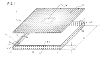
- Fig. 1 is an exploded perspective view of the light source device according to the first embodiment of the present invention.
- the light source device 1 is composed of a point light source 2, a box-shaped housing 3 that is provided, at a bottom plate thereof, with the point light source and is open at top, and an optical reflective plate 4 that covers the opening of the housing and reflects and transmits light from the point light source 2.
- a single piece of LED or an LED assembly of a plurality of LED elements (these are hereinafter collectively called LED), or an LD is used.
- the LED may be not only in one of the three primary colors R, G, and B, but also in another color.
- the LED or the LD may be equipped with a lens. In the present embodiment, examples using the LED will be described.
- the housing 3 has a box shape that includes a housing bottom plate 3a to substantially central part of which an LED 2 is fixed, housing side plates 3b to 3e that are arranged in a standing manner from a periphery of the housing bottom plate to a predetermined height, and a side defining an opening 3f provided facing the housing bottom plate.
- Inner wall surfaces of the housing 3 are formed with reflective surfaces.
- External wall surfaces of the housing side plates 3b to 3e are preferable to be also formed with reflective surfaces.
- the housing 3 is formed of a reflective plate material, such as an ultrafinely foamed optical reflective plate, that has a high optical reflectance, a low optical transmittance, and a low optical absorptance.
- a type of the ultrafinely foamed optical reflective plate material having an optical reflectance of 98%, an optical transmittance of 1%, and an optical absorptance of 1% is available, and preferable to be used.
- the material to be used for the housing is obviously not limited to this material.
- a transparent substrate on which reflective material is coated or printed may be used. Such a material is formed, for example, by coating or screen-printing an emulsion of fine particles of titanium white or an emulsion of fine particles of polytetrafluoroethylene.
- the housing bottom plate 3a has a substantially square shape with a side length of L1 (for example, 200 mm), and formed, at the substantially central part thereof, with an exposing hole that exposes a light-emitting part of the LED 2.
- the LED 2 is fixed to a mounting board (not illustrated), which in turn is arranged on the backside of the bottom plate so as to expose the light-emitting part of the LED through the exposing hole.
- the housing side plates 3b to 3e are formed of vertical plates that are arranged in a standing manner from the periphery of the substantially square-shaped bottom plate 3a to a predetermined height of h1 (for example, 15 mm). That is, side plates 3b to 3e are formed of four vertical plates.
- the housing side plates stand vertically, they may be inclined outward at a predetermined angle from the periphery of the housing bottom plate 3a.
- the inclination angle is preferably approximately more than 90° and not more than 150° between the side plate and a flat surface of the housing bottom plate 3a. With the inclination, the opening can be enlarged, and the LED light can be efficiently emitted to the opening side by using the inclined surfaces.
- All, one, or some of the four housing side plates 3b to 3e are each provided thereon with an optical reflective portion that emits the LED light to an outer surface side of the housing side plate substantially uniformly. A structure of the optical reflective portion will be described later.
- Fig. 2 illustrates the optical reflective plates constituting the light source device of Fig. 1 , with Fig. 2A being a top view, and Fig. 2B being a top view of a variation of the optical reflective plate.
- the optical reflective plate 4 is formed of a square plate-shaped body that closes the opening 3f of the housing 3.
- the optical reflective plate 4 is formed of the square plate-shaped body that has a predetermined thickness and identical side lengths of L1. That is, opposed sides 4a and 4b have the same length as that of 4c and 4d.
- the optical reflective plate 4 is provided with a central reflective portion 5A at a central part of the plate, and an outer reflective portion 5B around the outer perimeter of the central reflective portion, and is formed of a reflective plate, such as an ultrafinely foamed optical reflective plate material, that has a high optical reflectance, a low optical transmittance, and a low optical absorptance.
- a type of the ultrafinely foamed optical reflective plate material having an optical reflectance of 98%, an optical transmittance of 1%, and an optical absorptance of 1% is available, and preferable to be used.
- the central reflective portion 5A is located directly above the LED 2 when the optical reflective plate 4 is mounted at the opening 3f of the housing 3, and is composed of a central reflecting area 5a that has a small area and faces a vertically top portion of the light-emitting part of the LED, and of a pericentral reflecting area 5b that has a slightly enlarged area and is located at a predetermined distance apart from the central reflecting area 5a. Because of light distribution characteristics thereof, the LED 2 irradiates the strongest light to the central reflecting area 5a, and second strongest light to the pericentral reflecting area 5b.
- the central reflecting area 5a is adjusted to have the highest optical reflectance and the lowest optical transmittance
- the pericentral reflecting area 5b is adjusted to have a slightly lower optical reflectance and a slightly higher optical transmittance than those of the central reflecting area 5a. Because the central reflecting area 5a has the highest reflectance and the lowest optical transmittance, this area can be prevented from producing a high-luminance illumination spot while not being darkened.
- the optical reflectance and the optical transmittance are adjusted by processing the reflective plate.
- the optical reflectance and the optical transmittance are adjusted by applying processing such as providing a fine groove group composed of a plurality of fine grooves (longitudinal grooves, transverse grooves, and ring-shaped grooves) on the reflective plate material, or adjusting the plate thickness.
- the optical reflectance and the optical transmittance are adjusted by providing, for example, a fine hole group composed of a plurality of fine holes (through-holes having a diameter of, for example, 1.0 mm or less).
- the outer reflective portion 5B is provided with a plurality of through-holes 51 to 53 that have opening areas different from each other and are arranged with predetermined regularity from the pericentral reflecting area 5b toward the sides 4a to 4d.
- openings of the through-holes 51 to 53 the through-hole 51 located nearest to the pericentral reflecting area has the smallest opening area, and the opening area increases in the order of the through-holes 52 and 53 as the through-hole departs from the pericentral reflecting area.
- the through-holes having these openings are formed at places where parallel lines in parallel with the side 4a and vertical lines in parallel with the side 4b perpendicular to the side 4a intersect with each other. That is, the openings of these through-holes are arranged with regularity at even intervals in an orthogonal grid pattern.
- This optical reflective plate 4 had at four corners thereof through-holes each having a predetermined opening. However, it was found that, if the corner portions have the openings, the surface illuminating device is slightly dark at places corresponding to the corner portions when the light source device is embedded in the surface illuminating device described later. Therefore, an optical reflective plate 4A is provided with no openings in the predetermined areas at corner portions 6, as illustrated in Fig. 2B . By not providing the openings at the corner portions, more amount of reflected light is emitted from the optical reflective portions of the side plates corresponding to the corner portions. Thus, the above-described disadvantage is eliminated.
- the ultrafinely foamed optical reflective plate material has been exemplified as raw material of the optical reflective plate, the raw material is not limited to this material. Instead, a transparent substrate may be used on which reflective material is coated or printed except at the opening portions described above. Such a material is formed, for example, by coating or screen-printing an emulsion of fine particles of titanium white or an emulsion of fine particles of polytetrafluoroethylene.
- Fig. 3 illustrates the optical reflective portion of the side plate constituting the light source device of Fig. 1 , with Fig. 3A being one side view of Fig. 1 , and Figs. 3B to 3D being side views of respective variations of the optical reflective portion.
- the optical reflective portion 7A is composed of a side central reflective portion 7a that faces the LED 2 and is provided in an area nearest to the LED, and of a side outer reflective portion 7b that is provided in an area extended in the longitudinal direction from the side central reflective portion.
- the side central reflective portion 7a is provided with a plurality of fine holes so as to have a low optical transmittance while reflecting the outgoing light from the LED at a high optical reflectance.
- the side outer reflective portion 7b is provided with through-holes each of which has an opening that gradually reduces the optical reflectance and increases the optical transmittance as the through-hole departs from the side central reflective portion 7a.
- the fine holes and the through-holes are formed using substantially the same methods as those for the central reflective portion 5A and the outer reflective portion 5B of the optical reflective plate 4.
- the optical reflective portion 7A may be rougher than and not so elaborate as the optical reflective plate 4. This is because the light irradiated to the housing side plate is weaker than that directly above the LED due to the light distribution characteristics of the LED 2.
- the optical reflective portion is not limited to the optical reflective portion 7A, but may be changed variously.
- a side central reflective portion 7a1 and a side outer reflective portion 7b1 are provided with slits, each of which is changed in area so as to give a predetermined opening ratio (refer to Fig. 3B ).
- An optical reflective portion 7C is structured to be provided with no slit at a side central reflective portion 7a2, but is provided with a relatively long slit with an opening area thereof enlarged in the longitudinal direction at a side outer reflective portion 7b2 (refer to Fig. 3C ).
- An optical reflective portion 7D is structured to be provided with no notch at a side central reflective portion 7a3, but is provided with a notch that is wider as it goes outward in the longitudinal direction at a side outer reflective portion 7b3 (refer to Fig. 3C ).
- the optical reflective portion is provided on each of the four housing side plates 3b to 3e.
- the optical reflective portion need not be provided on every one of the side plates, but may be provided on one or several of the side plates depending on the necessity of illumination light from the side faces.
- the optical reflective portion is provided with the through-holes, the slits, and the notch that have the predetermined openings. Because these openings penetrate the side plate, dust or the like may enter from these portions depending on the use environment. In such a use environment, it is preferable to use a transparent substrate for the housing side plate, and to structure the side plate by coating or printing the reflective material on the substrate.
- the light source device 1 can emit the light from the LED 2 not only through the surface of the optical reflective plate 4 but also through the surfaces of the side plates of the housing 3 substantially uniformly, the light source device 1 can be used by being embedded not only in the surface illuminating device to be described later but also in an automatic vending machine or a large-size game machine.
- Fig. 4 is a schematic top view of the surface illuminating device according to the second embodiment of the present invention
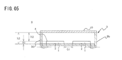
- Fig. 5 is a cross-sectional view obtained by cutting along a line V-V of Fig. 4 .
- Fig. 4 illustrates the surface illuminating device with a diffusion plate removed so that the inside can be seen.
- a surface illuminating device 8 includes four light source devices 1, a container case 9 that contains the light source devices, and a diffusion plate 10 that closes an opening of the container case and diffuses outgoing light from the light source devices.
- the surface illuminating device 8 is structured such that the four light source devices 1 are arranged in the container case 9 with a predetermined clearance (distance) between each other, and the opening of the container case 9 is covered with the diffusion plate 10.
- the container case 9 includes a case bottom plate 9a that has a larger area than a total area obtained by summing a bottom area of each of the light source devices 1, case side plates 9b to 9e that are arranged in a standing manner from a periphery of the case bottom plate, and a side defining an opening 9f provided facing the case bottom plate. Inner wall surfaces of the container case 9 are formed with reflective surfaces.
- the case bottom plate 9a has a larger area than a total area obtained by summing a bottom plate area of each of four housings 3 constituting the light source devices 1.
- the length of a side of the case bottom plate 9a is greater than a total length obtained by summing the length L1 in the longitudinal direction of each of the housing side plates.
- a height h3 of the case side plate is greater than the height h1 of the housing side plate, as illustrated in Fig. 5 .
- the height h2 is denoted as a clearance D3 between the diffusion plate and the optical reflective plate of the light source device.
- the surface illuminating device 8 is embedded as follows: In the container case 9, the four light source devices 1 are arranged with a predetermined clearance (distance) G1 between adjacent devices and with a clearance (distance) G2 between the device and the case side plate, and then, the opening 9f is covered with the diffusion plate 10, which is then fixed.
- G1 is denoted as a clearance D2 between the light source devices
- G2 is denoted as a clearance D1 that allows the illumination light to be emitted between the inner wall surfaces and the light source devices.
- the clearance (distance) h2 is formed between a light-emitting surface of each of the light source devices 1 and the diffusion plate 10.
- the relationships among the distances G1, G2, and h2 are important for obtaining uniform illumination light from an outer surface of the diffusion plate 10. That is, increasing the distances G1 and G2 darkens the area between the adjacent light source devices 1 and the area between the case side plate of the container case 9 and the light source devices 1, and increasing the height h2 makes it impossible to obtain a desired illuminance.
- the housing side plates of the light source device are provided with the optical reflective portions.
- the area of the light-emitting surface can be larger, and the device can be shorter in height than in the above case (a). That is, each of the light source devices 1 emits substantially uniform LED light from the housing side plates 4b to 4e thereof through the optical reflective portions 7, and the emitted light is reflected in the clearance between the adjacent devices and by the inner wall surfaces of the container case 9 and then goes out from the diffusion plate 10. Consequently, the clearances G1 and G2 can be larger than those in the above case (a).
- G1 can be set to a half or more of the maximum distance W between opposed side plates of the light source device 1 (refer to Fig.
- G2 can be set to a half or more of G1; and h2 can be set to a half or less of G1.
- the side plates 9b to 9e of the container case 9 are arranged in a vertically standing manner from the case bottom plate 9a.
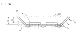
- the side plates may be inclined outward at a predetermined angle from the periphery of the case bottom plate 9a as illustrated by a surface illuminating device 8A (refer to Fig. 6 ).
- the inclination angle is preferably approximately more than 90° and not more than 150° between the side plate and a flat surface of the case bottom plate 9a. With this inclination, the opening and a diffusion plate 10A are enlarged, and thus, a light emission area is increased.
- a height h2' can be smaller (h2' ⁇ h2).
- the side plates of the container case have a flat plate shape, they may be curved toward the inside of the case. In this case, if the inner walls of the container case are formed with reflective surfaces such as mirror surfaces, the light can be radiated more efficiently from the opening of the container case.
- the side plates can also have a corrugated shape or other shapes instead of the flat plate shape.
- the surface illuminating devices 8 and 8A of the above-described embodiment are composed of the four light source devices 1.
- the number of the devices can be changed corresponding to the purpose of use.
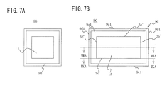
- the surface illuminating device may be structured by containing a single piece of the light source device 1 in a container case 9B for one device like a surface illuminating device 8B (in Fig. 7A ).
- the surface illuminating devices 8, 8A, and 8B of the above-described embodiment are structured such that the light source device 1 has a substantially square shape, and the container cases 9, 9A, and 9B containing the light source device(s) have a substantially square shape. However, they may have any shape, such as a non-square rectangular shape as illustrated in Fig. 7B .
- FIG. 7B is a schematic top view of the surface illuminating device.
- Fig. 8A is a cross-sectional view along a line VIIIA-VIIIA of Fig. 7B
- Figs. 8B and 8C are side views of optical reflective portions provided on side plates. Note that Fig. 7B illustrates the surface illuminating device with a diffusion plate removed so that the inside can be seen.
- a surface illuminating device 8C is composed of a light source device 1A having a non-square rectangular shape, a container case 9C that contains the light source device, and a diffusion plate 10B (refer to Fig. 8A ) that covers an opening of the container case.
- the light source device 1A, the container case 9C, and the diffusion plate 10B are the same in structure as, though different in shape from, the light source device 1, the container case 9, and the diffusion plate 10 of the surface illuminating device 8 described above. Therefore, descriptions thereof will be omitted.
- the light source device 1A includes a pair of opposed short housing side plates 3b' and 3d' and a pair of opposed long housing side plates 3c' and 3e'. These housing side plates are each provided with an optical reflective portion.
- the housing side plates 3b' and 3d' and the housing side plates 3c' and 3e' have mutually different approach distances to the LED 2. Therefore, the long housing side plates 3c' and 3e' are each provided with an optical reflective portion 7A' that is composed of a side central reflective portion 7a' and side outer reflective portions 7b'. Because the short housing side plates 3b' and 3d' are farther from the LED 2, no processing is required to form reflective portions such as the side central reflective portion 7a' and the side outer reflective portion 7b'. Instead, an optical reflective portion 7E is provided that is provided with through-holes having the same opening area as each other.
- FIG. 9 illustrates a light source device and a surface illuminating device using same light source device according to the third embodiment of the present invention, with Fig. 9A being a schematic top view, Fig. 9B being one side view of the surface illuminating device of Fig. 9A , and Fig. 9C being a cross-sectional view along a line IXC-IXC of Fig. 9A .
- Fig. 10 illustrates a variation of the surface illuminating device of Fig. 9A , with Fig. 10A being a top view, and Fig. 10B being a cross-sectional view along a line XB-XB of Fig. 10A .
- Figs. 9A and 10A each show the surface illuminating device with a diffusion plate removed so that the inside can be seen.
- a part of the structure of each of the light source devices 1 and 1A, and the surface illuminating devices 8, 8B, and 8C that use the light source device(s) is changed corresponding to the purpose of use.
- a surface illuminating device 8D is composed of a light source device 1B, a container case 9D that contains the light source device 1B, and a diffusion plate (not illustrated) that covers an opening of the container case. Note that this surface illuminating device is obtained by cutting the surface illuminating device 8C of Fig. 7B along a line 1XA-IXA and by changing a part of the structure thereof.
- the light source device 1B has four housing side plates 3b1 to 3e1.
- the housing side plates 3e1, 3b1, and 3d1 of the housing side plates 3b1 to 3e1 are each provided with an optical reflective portion.
- the housing side plate 3c1 is formed of only a plate body without being provided with an optical reflective portion.
- the container case 9D includes a case bottom plate 9a, case side plates 9b1 to 9e1 that are arranged in a standing manner from a periphery of the case bottom plate, and a side defining an opening 9f provided facing the case bottom plate. Inner wall surfaces of the container case 9D are formed with reflective surfaces.
- One side plate 9c1 of the case side plates is provided with a slit 9c1' that allows light from the light source device 1B to pass therethrough.
- the slit 9c1' is provided with an opening area defined by a length equal to or slightly greater than that of a long side plate of the light source device and by a predetermined width.
- the illumination light is also irradiated from the slit 9c1'.
- the surface illuminating device 8D is used by being embedded in, for example, a game machine.
- the case side plates 9b1 to 9e1 of the container case 9 are arranged in a vertically standing manner from the case bottom plate 9a1.
- Case side plates 9b1', 9d1', and 9e1' of a container case 9E may be inclined outward at a predetermined angle from the periphery of the case bottom plate 9a1 as illustrated by a surface illuminating device 8E (refer to Figs. 10A and 10B ).
- the inclination angle is preferably approximately more than 90° and not more than 150° between the side plate and a flat surface of the case bottom plate 9a1. With this inclination, the opening and the diffusion plate 10B are enlarged, and thus, the light emission area is increased.
- case height h2' can be further decreased (h2' ⁇ h2).
- the side plate 9c1 is arranged in a vertically standing manner from the case bottom plate 9a1 because the side plate 9c1 is not provided with a reflective portion but provided with the slit 9c1'.
- FIG. 11 is an external perspective view of a light source device used in a surface illuminating device according to a fourth embodiment of the present invention.
- a box-shaped housing 3 is provided with a housing bottom plate 3a whose inner surface is formed with a reflective member, provided with housing side plates 3b to 3e that are arranged in a standing manner from a periphery of the housing bottom plate 3a and are formed on the inner and outer surfaces thereof with reflective members, and provided with a side defining an opening provided facing the housing bottom plate 3a.
- a light source device 1C is composed of the housing 3, a point light source 2 that is fixed to the housing bottom plate 3a, and an optical reflective plate 4 that covers the opening of the housing 3, and reflects and transmits light from the point light source 2.
- the four housing side plates 3b, 3c, 3d, and 3e are arranged in a vertically standing manner from the housing bottom plate 3a.
- the light source device 1C has a height of h1, and the housing side plates 3b, 3c, 3d, and 3e have the same length of L1.
- the housing 3 and the optical reflective plate 4 are each formed of a material, such as an ultrafinely foamed transmissive/reflective member, that has a high optical reflectance, a low optical transmittance, and a low optical absorptance.
- a type of the ultrafinely foamed transmissive/reflective member having an optical reflectance of 98%, an optical transmittance of 1%, and an optical absorptance of 1% is available.
- Other usable materials include a material formed by coating or screen-printing an emulsion of fine particles of titanium white or an emulsion of fine particles of polytetrafluoroethylene.
- a coated film containing fine particles of titanium white or polytetrafluoroethylene is also suitable.
- an LED or an LED group composed of a plurality of LEDs, or an LD is used as the point light source 2 used in the light source device 1C.
- the LED and the LD has high directionality, but uniform illumination light can be obtained at the top face by adjusting the transmittance of the optical reflective plate 4. Because the optical reflective plate 4 used in the present fourth embodiment is the same as that used in the first embodiment, descriptions thereof will be omitted.
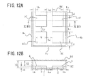
- Fig. 12A is a top view of the surface illuminating device according to the fourth embodiment
- Fig. 12B is a cross-sectional view obtained by cutting along a line XIIB-XIIB of Fig. 12A
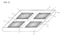
- Fig. 13 is an external perspective view of the surface illuminating device according to the fourth embodiment of the present invention.
- the light source devices are arranged in the container case 9 with predetermined distances La and Lc between each other.
- the distances La and Lc have the same value of a half or less of a maximum distance W between opposed side plates of the light source device. A distance of more than this value makes it difficult to obtain uniform illumination light.
- distances Lb and Ld are provided between the light source devices and container case side faces 9a, 9b, 9c, and 9d.
- the distances Lb and Ld have the same value of a half of the distances La and Lc. This is because the container case side faces 9a to 9d have no light source and hence illumination from the side faces is not obtained.
- the light emitted from the outer reflective portion 5B illuminates above the outer part of the light source device and a top surface S of a face where the light source device is not placed.
- the light from the central reflective portion 5A of the light source device illuminates above the central part of the surface illuminating device. Because the light from the outer reflective portion 5B illuminates the top surface S, the illuminance of the top surface S increases whereas the illuminance above the outer part of the light source device decreases, and thus, the illuminance of the surface illuminating device becomes uniform as a whole.
- the overall illuminance is further uniformed by providing the diffusion plate 10.
- the diffusion plate 10 is provided at a predetermined clearance h2 from the optical reflective plate 4.
- the clearance h2 between the diffusion plate 10 and the optical reflective plate 4 is preferably a half or more of the predetermined distances La and Lc between the light source devices.
- light is noticeably uneven with the clearance h2 that is a half or less of the predetermined distances La and Lc.
- optical reflective plate 4 used in the fourth embodiment described above can provide uniform illumination light
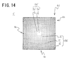
- Fig. 14 is a front view of the optical reflective plate 4' in a light source device (not illustrated) used in a light source device of a fifth embodiment of the present invention.
- the optical reflective plate 4' has almost the same structure as that of the optical reflective plate 4 in the fourth embodiment, and thus, descriptions of the same parts will be omitted.
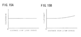
- FIG. 15A is a graph showing a relationship between a distance from the light source and the illuminance in the case in which the optical reflective plate 4 is used
- Fig. 15B is a graph showing a relationship between the distance from the light source and the illuminance in the case in which the optical reflective plate 4' is used.
- the size of the opening of light source device 1' of the fifth embodiment is determined so that the illuminance is higher as the distance is longer from the light source.
- the optical reflective plate 4 which can provide uniform illumination light over the entire light source device, the illumination light hardly reaches the top surface above the place where the light source device 1C is not located. Accordingly, when the diffusion plate 10 is arranged at a near place, the surface illuminating device gives a slightly unevenly distributed illumination as an entire surface illuminating device in which the light source devices 1C are arranged side by side. Therefore, in the fifth embodiment, the optical reflective plate 4' is used that is processed so that the illuminance is higher in the outer part than in the central part.
- the obtained illumination light can be uniform as that of an entire surface illuminating device even if a single light source device emits uneven illumination light.
- Fig. 16 is an external perspective view of a light source device 1D in a sixth embodiment
- Fig. 17 is an external perspective view of a surface illuminating device in which the light source devices ID in the present embodiment are arranged side by side.
- sidewall portions 30b, 30c, 30d, and 30e of the light source device 1D are each provided with openings H1, H2, and H3.
- sidewall portions 90a, 90b, 90c, and 90d of a container case are arranged in a standing manner not vertically but obliquely at an inclination angle of approximately 45 degrees from the vertical direction.
- the sidewall portions 90a to 90d are each formed of a material, such as an ultrafinely foamed transmissive/reflective member, that has a high optical reflectance, a low optical transmittance, and a low optical absorptance.
- a material such as an ultrafinely foamed transmissive/reflective member, that has a high optical reflectance, a low optical transmittance, and a low optical absorptance.
- a type of the ultrafinely foamed transmissive/reflective member having an optical reflectance of 98%, an optical transmittance of 1%, and an optical absorptance of 1% is available.
- Other materials may be used, such as an emulsion of fine particles of titanium white and an emulsion of fine particles of polytetrafluoroethylene. These materials may be coated or screen-printed on the housing.
- Part of light is transmitted through the openings H1, H2, and H3, and reflected by the sidewall portions 90a to 90d of the container case. Thereby, a top surface S of a face where the light source device is not placed is illuminated, and thus, more uniform illumination light can be obtained.
- the housing has a rectangular shape in a plan view.
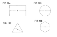
- the housing is not necessarily limited to have a rectangular shape, but can have various shapes, such as a triangular shape, a honeycomb shape, and a circular shape, in a plan view as illustrated in Fig. 18.
- Fig. 18 illustrates top views of light source devices that can be used in surface illuminating devices of variations in the embodiments 4 to 6 of the present invention.
- a predetermined distances La and Lc between the light source devices are also a half or less of a maximum distance W between opposed side plates of the light source device in the same manner as in the above-described embodiments.
- a clearance h2 between the diffusion plate and the light source device is also a half or more of the predetermined distances La and Lc.
Abstract
Description
- The present invention relates to a light source device and a surface illuminating device using same light source device, and more in detail, to a light source device that can emit substantially uniform illumination light while using a point light source having high directionality as a light source, and surface illuminating device using same light source device.
- In recent years, as an alternative to traditional incandescent light bulbs and fluorescent lamps, a illuminating device using a point light source having high directionality, such as a light-emitting diode (hereinafter called LED) or a laser diode (hereinafter called LD), has been developed and is beginning to be used in a display device and the like. The LED has excellent features such as being more power-saving, longer-lived, and smaller than other illuminating devices such as the incandescent light bulbs and the fluorescent lamps. The LED, however, has drawbacks such as having an extremely small illumination area due to high directionality, and giving damage to eyes looking directly at the light emitted from the LED. Consequently, in order to use the LED for illumination light, a technology for efficiently diffusing the light is required. Therefore, in order to use such a point light source for illumination light, there are proposed illuminating devices in which various contrivances are used (refer to, for example,
Patent Documents 1 and 2 bellow). - For example, Patent Document 1 listed below describes a surface light-emitting device that enables to provide surface light by mounting, on an LED, light control means that controls light emitted from the LED.
- This surface light-emitting device includes: LEDs; a rectangular solid-shaped case that houses the LEDs; light control means mounted on an external surface of a lens of each of the LEDs; and a diffusion panel that covers an opening of the case. The case is structured as follows: a reflector is arranged in the case; the plurality of LEDs are arranged on a bottom of the reflector at predetermined intervals each other; the light control means is mounted on each of the LEDs; and the opening of the case is covered by the diffusion panel. The light control means is composed of a main reflective portion that is located in a position corresponding to the center of the LED, and reflects and transmits the light emitted from the LED at a greater reflection amount than a transmission amount, of a reflective/transmissive portion that is located around the main reflective portion and transmits a greater amount of light than that of the main reflective portion, and of a holder portion provided at the main reflective portion.
-
Patent Document 2 listed below describes a surface lighting light source device, and a surface illuminating device using the surface lighting light source device. - This surface lighting light source device is composed of an LED, of a box-shaped casing that has a bottom surface portion provided at a central part thereof with the LED, side face portions arranged in a standing manner from a periphery of the bottom surface portion, and a side defining an opening provided facing the bottom surface portion, and of an optical reflective plate that covers the opening and makes the light from the LED substantially uniform. The surface illuminating device uses a plurality of such surface lighting light source devices which are adjacently connected with each other.
- When the plurality of surface lighting light source devices are adjacently connected with each other, adjacently connected portions are dark. Therefore, for example, Patent Document 3 listed below discloses a surface illuminating device in which the adjacently connected portions are provided at sidewall portions thereof with sidewall holes. The sidewall holes are communicated to the opening. Note that
Patent Documents 2 and 3 listed below are the patent applications filed by the applicant of the present application. -
- Patent Document 1: Japanese Patent Application Publication No.
2004-006317 Fig. 1 ) - Patent Document 2: Japanese Patent Application Publication No.
2008-027886 Fig. 1 ) - Patent Document 3: Japanese Patent Application Publication No.
2009-110696 Fig. 8 ) - All of the surface light-emitting devices and the surface illuminating devices of Patent Documents 1 to 3 have a structure in which a plurality of light source devices are closely in contact with each other without a space between the adjacent devices. In order to increase an area of a light-emitting surface, that is an illumination area, of these surface illuminating devices, more of the light source devices are to be installed. In such additional installation, if a plurality of additional light source devices are installed closely in contact with each other as have been installed before, the area of the light-emitting surface cannot be increased as much as an increase in cost for the additional installation. That is, the area of the light-emitting surface is at most the total of areas of the light-emitting surfaces of the light source devices thus increased. It can be contrived to arrange the light source devices not in contact with each other but with a predetermined space between the adjacent light source devices. However, in that case, the space is dark, and the dark portion is projected on a diffusion plate. Thus, dark lines or the like appear on the light-emitting surface. In order to solve this problem, the diffusion plate arranged above the light source device must be raised, that is, the distance of the diffusion plate from the light-emitting surface must be increased. As a result, problems arise such that the surface illuminating device becomes tall. This problem cannot be solved even with the surface illuminating device of Patent Document 3 described above. In the case of additional installation of the surface light-emitting devices of Patent Document 1 described above, the rectangular solid-shaped cases housing the reflector are to be added. Therefore, the number of the LEDs cannot be adjusted in the additional installation.
- The light source device using the LED has advantages such as being power-saving, long-lived, and small-sized thanks to the features of the LED in recent years. Examples of applications of such a light source device are therefore not limited to the use cases as described above in Patent Documents 1 to 3 but also may include these devices embedded in an automatic vending machine or a large-size game machine. However, when embedded without any special consideration, the light source device provides only a limited illumination area because it has the light-emitting surface only on one face, that is, only on the top face. Thus, such a light source device cannot be used when a peripheral area needs to be illuminated.
- In addition to the above-described problems, in the inventions disclosed by
Patent Documents 1 and 2, there has been the following problem. The surface lighting light source devices are arranged without a space between each other. Therefore, when the surface to be illuminated is large, a very large number of the surface lighting light source devices are arranged, thus resulting in high cost. - In order to reduce such cost, various methods can be considered. The methods include: to degrade the quality of the LED and/or the reflective plate, to stop using the diffusion plate, and to reduce the size of the illumination surface, for example.
- However, degrading the quality of the LED leads to an increase in failure rate, or a failure in obtaining uniform light emission. Therefore, the life as a illuminating device is shortened and a variation in brightness of the illumination light increases. Degrading the quality of the reflective plate leads to occurrence of disadvantages, such as difficulty in obtaining uniform illumination light due to insufficient reflection, and darkening of the illumination light.
- If the reflective plate is not used, it is also difficult to obtain uniform illumination light, in the same manner as in the case of degrading quality of the reflective plate. Though reducing the size of the illumination surface leads to a cost reduction, it becomes impossible to illuminate an intended area. In this case, such illuminating device does not fulfill its role.
- In order to solve the problems of the conventional technologies described above, it is an object of the present invention to provide a light source device that can be used for multiple purposes by enabling to emit illumination light from multiple faces.
- It is another object of the present invention to provide a surface illuminating device at low cost that can provide uniform illumination light over a large area without increasing a thickness (that is, a height from the light source) of the surface illuminating device, by using the above-described light source device.
- It is still another object of the present invention to provide a low-cost surface illuminating device that can provide uniform illumination light over a large screen while minimizing a reduction in luminance, when arranging a plurality of such light source devices, not by adjacently arranging the light source devices, but by arranging them at a predetermined distance apart from each other as well as by arranging the diffusion plate at a larger distance from the light source device than in the case of a conventional diffusion plate.
- In order to achieve the above-described objectives, a light source device of a first aspect of the present invention includes: a point light source having high directionality; a housing that has a housing bottom plate arranged with the point light source, housing side plates arranged in a standing manner from a periphery of the housing bottom plate to a predetermined height, and a side defining an opening provided facing the housing bottom plate, and that is formed on inner wall surfaces thereof with reflective surfaces; and an optical reflective plate that covers the opening and emits light from the point light source as substantially uniform illumination light, each of at least some of the housing side plates being provided with a side central reflective portion having a high optical reflectance and a low optical transmittance in a side plate region nearest to the point light source, and provided, in outer side plate regions of the side central reflective portion, with side outer reflective portions that have an optical reflectance decreasing and an optical transmittance increasing as being distant from the side central reflective portion.
- In the light source device of the first aspect of the present invention, it is preferable that, in the housing, the housing bottom plate have a rectangular shape, and at least one of the housing side plates arranged in a standing manner from the periphery of the rectangular shape be provided with the side central reflective portion and the side outer reflective portions.
- In the light source device of the first aspect of the present invention, it is also preferable that the side central reflective portion be provided with grooves formed by half-cutting the housing side plate or with fine holes, and the side outer reflective portions be provided with through-holes that penetrate the housing side plate and have a predetermined opening area.
- In the light source device of the first aspect of the present invention, it is also preferable that the point light source be a light-emitting diode or a laser diode.
- In addition, in order to achieve the above-described objectives, a surface illuminating device of a second aspect of the present invention includes one or more of the light source devices, a container case that is provided with an opening and a size capable of containing one or more of the light source devices, and a diffusion plate that covers the opening. The container case is a box body including a case bottom plate that has a larger area than a total of bottom areas of the contained number of the light source devices, case side plates that are arranged in a standing manner from a periphery of the case bottom plate to a height larger than that of the housing side plates of the light source device, and a side defining the opening provided facing the case bottom plate, with inner wall surfaces of the box body formed with reflective surfaces. The light source device is arranged in the container case with a clearance (D1) that allows the illumination light to pass between the inner wall surface and the light source device.
- In the surface illuminating device of the second aspect of the present invention, it is preferable that the case side plates be inclined outward at 90° to 150° from a flat surface of the case bottom plate.
- In the surface illuminating device of the second aspect of the present invention, it is also preferable that the container case contain the plurality of light source devices with adjacent light source devices being arranged with a predetermined clearance (D2) between each other, and the diffusion plate be arranged with a predetermined clearance (D3) from the optical reflective plate of each of the plurality of light source devices.
- In the surface illuminating device of the second aspect of the present invention, it is also preferable that the clearance (D2) be a half or more of a maximum distance (W) between opposed side plates of the light source device, the clearance (D1) be a half or more of the clearance (D2), and the clearance (D3) be a half or less of the distance (D2).
- Furthermore, in order to achieve the above-described objectives, a surface illuminating device of a third aspect of the present invention includes a point light source, light source devices each of which has a box-shaped housing provided with a housing bottom plate whose inner surface side on which the point light source is fixed is reflective, with housing side plates that are arranged in a standing manner from a periphery of the housing bottom plate to a predetermined height and are reflective on the inner and outer surface sides thereof, with a side defining an opening provided facing the housing bottom plate, and with an optical reflective plate that covers the opening of the housing, and that reflects and transmits light from the point light source; a container case with an opening that is reflective on the inner surface side thereof and contains the plurality of light source device; and a diffusion plate that covers the opening of the container case. Adjacent light source devices among the light source devices are arranged with a predetermined clearance (D2) between each other, and the diffusion plate is arranged with a predetermined clearance (D3) from each of the optical reflective plates of the plurality of light source devices.
- In the surface illuminating device of the third aspect of the present invention, it is preferable that the predetermined clearance (D2) be a half or less of a maximum distance (W) between opposed side plates of the light source devices.
- In the surface illuminating device of the third aspect of the present invention, it is also preferable that the predetermined clearance (D3) be a half or more of the predetermined clearance (D2).
- In the surface illuminating device of the present invention, the housing side plate may be provided with an opening that allows part of light to be transmitted.
- In the surface illuminating device of the third aspect of the present invention, it is also preferable that the optical reflective plate have a transmittance increasing and a reflectance decreasing as a distance increases from the point light source.
- In the surface illuminating device of the third aspect of the present invention, it is also preferable that the housing and the optical reflective plate include ultrafinely foamed optical reflective members.
- In the surface illuminating device of the third aspect of the present invention, it is also preferable that the housing have any one of a rectangular shape, a triangular shape, a circular shape, and a honeycomb shape in a plan view.
- In the surface illuminating device of the third aspect of the present invention, it is also preferable that the container case have a similar shape to the housing.
- With the light source device of the first aspect of the present invention, the light from the point light source can be emitted not only from the surface of the optical reflective plate but also from the surface of the housing side plate substantially uniformly. As a result, the light-emitting surface becomes multifaceted and the light emission area increases. Accordingly, the light source device can be used in the surface illuminating device so as to enlarge the illumination area, and can also be embedded in equipment such as an automatic vending machine or a large-size game machine without any special consideration so as to enlarge the illumination area.
- Also, with the light source device of the first aspect of the present invention, the side central reflective portion is provided with grooves formed by half-cutting the side plate or with fine holes, and the side outer reflective portion is provided with through-holes that penetrate the side plate and have a predetermined opening area. Therefore, the side central reflective portion and the side outer reflective portions can be produced easily.
- In addition, the light source device of the first aspect of the present invention can provide uniform illumination light even with the point light source having high directionality, such as an LED or an LD, eliminating the possibility of leaving a bright spot at a central part or darkening a part directly above the point light source.
- With the surface illuminating device of the second aspect of the present invention, the respective effects of the light source device according to the above descriptions can be provided, and in addition, by arranging the plurality of light source devices, it is possible to obtain a surface illuminating device that can achieve illumination light having a uniform illuminance distribution covering a wider area.
- Also, with the surface illuminating device of the second aspect of the present invention, the case side plates are inclined outward. Therefore, the area of the case opening is larger than that of the case bottom plate, and in addition, the light radiated from the side of the light source device can be efficiently reflected toward the case opening.
- In addition, with the surface illuminating device of the second aspect of the present invention, the light source devices are not arranged adjacent to each other in the container case. Therefore, it is possible to obtain uniform illumination light over a large screen while minimizing a reduction in luminance by using a smaller number of the point light sources.
- With the surface illuminating device of the third aspect of the present invention, the light source devices are not arranged adjacent to each other in the container case. Therefore, it is possible to obtain uniform illumination light over a large screen while minimizing a reduction in luminance.
- Also, with the surface illuminating device of the third aspect of the present invention, it is possible to appropriately determine a distance between the light source devices and a clearance between the optical reflective plate and the diffusion member.
- In addition, with the surface illuminating device of the third aspect of the present invention, unevenness of light is suppressed even if the diffusion member is located closer, and thus, more uniform illumination light can be obtained.
- In the surface illuminating device of the present invention, it is possible to use the housing bottom plate, the housing side plates, and the optical reflective plate that are made of the same material. Using these plates of the same material makes production of them easy because the housing can be formed of a single material.
- Also, with the surface illuminating device of the present invention, it is possible to provide variously shaped surface illuminating devices that can provide uniform illumination light.
-
- [
Fig. 1] Fig. 1 is an exploded perspective view of a light source device according to a first embodiment of the present invention. - [
Fig. 2] Fig. 2A is a top view of an optical reflective plate constituting the light source device ofFig. 1 , andFig. 2B is a top view of a variation of the optical reflective plate. - [
Fig. 3] Fig. 3A is one side view of an optical reflective portion of a side plate constituting the light source device ofFig. 1 , andFigs. 3B to 3D are side views of respective variations of the optical reflective portion of the side plate. - [
Fig. 4] Fig. 4 is a schematic top view of a surface illuminating device according to a second embodiment of the present invention. - [
Fig. 5] Fig. 5 is a cross-sectional view obtained by cutting along a line V-V ofFig. 4 . - [
Fig. 6] Fig. 6 is a cross-sectional view illustrating a variation of the surface illuminating device ofFig. 4 . - [
Fig. 7] Figs. 7A and 7B are schematic top views of respective variations of the surface illuminating device ofFig. 4 . - [
Fig. 8] Fig. 8A is a cross-sectional view along a line VIIIA-VIIIA ofFig. 7B , andFigs. 8B and 8C are side views of optical reflective portions provided on side plates. - [
Fig. 9] Fig. 9A is a schematic top view of a light source device and a surface illuminating device using same light source device according to a third embodiment of the present invention,Fig. 9B is one side view of the surface illuminating device ofFig. 9A , and Fig. 9C is a cross-sectional view along a line IXC-IXC ofFig. 9A . - [
Fig. 10] Fig. 10A is a top view of a variation of the surface illuminating device ofFig. 9A , andFig. 10B is a cross-sectional view along a line XB-XB ofFig. 10A . - [
Fig. 11] Fig. 11 is an external perspective view of a surface lighting light source device used in a surface illuminating device according to a fourth embodiment of the present invention. - [
Fig. 12] Fig. 12A is a top view of the surface illuminating device according to the fourth embodiment of the present invention, andFig. 12B is a cross-sectional view obtained by cutting along a line XIIB-XIIB ofFig. 12A . - [
Fig. 13] Fig. 13 is an external perspective view of the surface illuminating device according to the fourth embodiment of the present invention. - [
Fig. 14] Fig. 14 is a front view of an optical reflective plate used in a light source device of a fifth embodiment of the present invention. - [
Fig. 15] Fig. 15A is a graph showing a relationship between a distance from a light source and illuminance in the case in which an ordinary optical reflective plate is used, andFig. 15B is a graph showing a relationship between the distance from the light source and illuminance in the case in which an optical reflective plate used is processed so that illuminance is higher in a peripheral part than in a central part. - [
Fig. 16] Fig. 16 is an external perspective view of a light source device used in a surface illuminating device according to a sixth embodiment of the present invention. - [
Fig. 17] Fig. 17 is an external perspective view of the surface illuminating device according to the sixth embodiment of the present invention. - [
Fig. 18] Fig. 18 illustrates top views of light source devices that can be used in surface illuminating devices of variations in theembodiments 4 to 6 of the present invention. - Embodiments of the present invention will be described below. It should be noted that the embodiments presented below are for exemplifying a light source device and a surface illuminating device using same light source device for realizing the technological concept of the present invention, and are not intended to limit the present invention to those devices exemplified below, but the present invention can be equally applied to other embodiments included in the scope of the claims.
- An outline of a light source device according to a first embodiment of the present invention will be described with reference to
Fig. 1. Fig. 1 is an exploded perspective view of the light source device according to the first embodiment of the present invention. - The light source device 1 is composed of a point
light source 2, a box-shaped housing 3 that is provided, at a bottom plate thereof, with the point light source and is open at top, and an opticalreflective plate 4 that covers the opening of the housing and reflects and transmits light from the pointlight source 2. - As the point
light source 2, a single piece of LED or an LED assembly of a plurality of LED elements (these are hereinafter collectively called LED), or an LD is used. The LED may be not only in one of the three primary colors R, G, and B, but also in another color. In addition, the LED or the LD may be equipped with a lens. In the present embodiment, examples using the LED will be described. - The housing 3 has a box shape that includes a
housing bottom plate 3a to substantially central part of which anLED 2 is fixed,housing side plates 3b to 3e that are arranged in a standing manner from a periphery of the housing bottom plate to a predetermined height, and a side defining anopening 3f provided facing the housing bottom plate. Inner wall surfaces of the housing 3 are formed with reflective surfaces. External wall surfaces of thehousing side plates 3b to 3e are preferable to be also formed with reflective surfaces. When a surface illuminating device is produced using same light source device 1 in which the external wall surfaces are formed with the reflective surfaces, LED light is reflected between the external wall surfaces and inner wall surfaces of a container case of the surface illuminating device, and thus, the light can be efficiently emitted to a diffusion plate side. The surface illuminating device will be described later. The housing 3 is formed of a reflective plate material, such as an ultrafinely foamed optical reflective plate, that has a high optical reflectance, a low optical transmittance, and a low optical absorptance. A type of the ultrafinely foamed optical reflective plate material having an optical reflectance of 98%, an optical transmittance of 1%, and an optical absorptance of 1% is available, and preferable to be used. The material to be used for the housing is obviously not limited to this material. A transparent substrate on which reflective material is coated or printed may be used. Such a material is formed, for example, by coating or screen-printing an emulsion of fine particles of titanium white or an emulsion of fine particles of polytetrafluoroethylene. - The
housing bottom plate 3a has a substantially square shape with a side length of L1 (for example, 200 mm), and formed, at the substantially central part thereof, with an exposing hole that exposes a light-emitting part of theLED 2. TheLED 2 is fixed to a mounting board (not illustrated), which in turn is arranged on the backside of the bottom plate so as to expose the light-emitting part of the LED through the exposing hole. Thehousing side plates 3b to 3e are formed of vertical plates that are arranged in a standing manner from the periphery of the substantially square-shapedbottom plate 3a to a predetermined height of h1 (for example, 15 mm). That is,side plates 3b to 3e are formed of four vertical plates. Note that, although the housing side plates stand vertically, they may be inclined outward at a predetermined angle from the periphery of thehousing bottom plate 3a. The inclination angle is preferably approximately more than 90° and not more than 150° between the side plate and a flat surface of thehousing bottom plate 3a. With the inclination, the opening can be enlarged, and the LED light can be efficiently emitted to the opening side by using the inclined surfaces. All, one, or some of the fourhousing side plates 3b to 3e are each provided thereon with an optical reflective portion that emits the LED light to an outer surface side of the housing side plate substantially uniformly. A structure of the optical reflective portion will be described later. - The optical reflective plate mounted at the opening of the housing will be described with reference to
Figs. 1 and2 . Note thatFig. 2 illustrates the optical reflective plates constituting the light source device ofFig. 1 , withFig. 2A being a top view, andFig. 2B being a top view of a variation of the optical reflective plate. - As illustrated in
Figs. 1 and2A , the opticalreflective plate 4 is formed of a square plate-shaped body that closes theopening 3f of the housing 3. The opticalreflective plate 4 is formed of the square plate-shaped body that has a predetermined thickness and identical side lengths of L1. That is,opposed sides reflective plate 4 is provided with a centralreflective portion 5A at a central part of the plate, and an outerreflective portion 5B around the outer perimeter of the central reflective portion, and is formed of a reflective plate, such as an ultrafinely foamed optical reflective plate material, that has a high optical reflectance, a low optical transmittance, and a low optical absorptance. A type of the ultrafinely foamed optical reflective plate material having an optical reflectance of 98%, an optical transmittance of 1%, and an optical absorptance of 1% is available, and preferable to be used. - The central
reflective portion 5A is located directly above theLED 2 when the opticalreflective plate 4 is mounted at theopening 3f of the housing 3, and is composed of a central reflectingarea 5a that has a small area and faces a vertically top portion of the light-emitting part of the LED, and of apericentral reflecting area 5b that has a slightly enlarged area and is located at a predetermined distance apart from the central reflectingarea 5a. Because of light distribution characteristics thereof, theLED 2 irradiates the strongest light to the central reflectingarea 5a, and second strongest light to thepericentral reflecting area 5b. Therefore, the central reflectingarea 5a is adjusted to have the highest optical reflectance and the lowest optical transmittance, and thepericentral reflecting area 5b is adjusted to have a slightly lower optical reflectance and a slightly higher optical transmittance than those of the central reflectingarea 5a. Because the central reflectingarea 5a has the highest reflectance and the lowest optical transmittance, this area can be prevented from producing a high-luminance illumination spot while not being darkened. - The optical reflectance and the optical transmittance are adjusted by processing the reflective plate. In the central reflecting
area 5a, the optical reflectance and the optical transmittance are adjusted by applying processing such as providing a fine groove group composed of a plurality of fine grooves (longitudinal grooves, transverse grooves, and ring-shaped grooves) on the reflective plate material, or adjusting the plate thickness. In thepericentral reflecting area 5b, the optical reflectance and the optical transmittance are adjusted by providing, for example, a fine hole group composed of a plurality of fine holes (through-holes having a diameter of, for example, 1.0 mm or less). - The outer
reflective portion 5B is provided with a plurality of through-holes 51 to 53 that have opening areas different from each other and are arranged with predetermined regularity from thepericentral reflecting area 5b toward thesides 4a to 4d. As for openings of the through-holes 51 to 53, the through-hole 51 located nearest to the pericentral reflecting area has the smallest opening area, and the opening area increases in the order of the through-holes side 4a and vertical lines in parallel with theside 4b perpendicular to theside 4a intersect with each other. That is, the openings of these through-holes are arranged with regularity at even intervals in an orthogonal grid pattern. - This optical
reflective plate 4 had at four corners thereof through-holes each having a predetermined opening. However, it was found that, if the corner portions have the openings, the surface illuminating device is slightly dark at places corresponding to the corner portions when the light source device is embedded in the surface illuminating device described later. Therefore, an opticalreflective plate 4A is provided with no openings in the predetermined areas atcorner portions 6, as illustrated inFig. 2B . By not providing the openings at the corner portions, more amount of reflected light is emitted from the optical reflective portions of the side plates corresponding to the corner portions. Thus, the above-described disadvantage is eliminated. - Although the ultrafinely foamed optical reflective plate material has been exemplified as raw material of the optical reflective plate, the raw material is not limited to this material. Instead, a transparent substrate may be used on which reflective material is coated or printed except at the opening portions described above. Such a material is formed, for example, by coating or screen-printing an emulsion of fine particles of titanium white or an emulsion of fine particles of polytetrafluoroethylene.
- Next, the optical reflective portion formed on the side plate will be described with reference to
Fig. 3 . Note thatFig. 3 illustrates the optical reflective portion of the side plate constituting the light source device ofFig. 1 , withFig. 3A being one side view ofFig. 1 , andFigs. 3B to 3D being side views of respective variations of the optical reflective portion. - Each of the four
housing side plates 3b to 3e is provided with an opticalreflective portion 7A. The opticalreflective portion 7A is composed of a side centralreflective portion 7a that faces theLED 2 and is provided in an area nearest to the LED, and of a side outerreflective portion 7b that is provided in an area extended in the longitudinal direction from the side central reflective portion. The side centralreflective portion 7a is provided with a plurality of fine holes so as to have a low optical transmittance while reflecting the outgoing light from the LED at a high optical reflectance. The side outerreflective portion 7b is provided with through-holes each of which has an opening that gradually reduces the optical reflectance and increases the optical transmittance as the through-hole departs from the side centralreflective portion 7a. The fine holes and the through-holes are formed using substantially the same methods as those for the centralreflective portion 5A and the outerreflective portion 5B of the opticalreflective plate 4. The opticalreflective portion 7A may be rougher than and not so elaborate as the opticalreflective plate 4. This is because the light irradiated to the housing side plate is weaker than that directly above the LED due to the light distribution characteristics of theLED 2. - The optical reflective portion is not limited to the optical
reflective portion 7A, but may be changed variously. In an opticalreflective portion 7B, a side central reflective portion 7a1 and a side outer reflective portion 7b1 are provided with slits, each of which is changed in area so as to give a predetermined opening ratio (refer toFig. 3B ). An opticalreflective portion 7C is structured to be provided with no slit at a side central reflective portion 7a2, but is provided with a relatively long slit with an opening area thereof enlarged in the longitudinal direction at a side outer reflective portion 7b2 (refer toFig. 3C ). An optical reflective portion 7D is structured to be provided with no notch at a side central reflective portion 7a3, but is provided with a notch that is wider as it goes outward in the longitudinal direction at a side outer reflective portion 7b3 (refer toFig. 3C ). - In the present embodiment, the optical reflective portion is provided on each of the four
housing side plates 3b to 3e. However, the optical reflective portion need not be provided on every one of the side plates, but may be provided on one or several of the side plates depending on the necessity of illumination light from the side faces. The optical reflective portion is provided with the through-holes, the slits, and the notch that have the predetermined openings. Because these openings penetrate the side plate, dust or the like may enter from these portions depending on the use environment. In such a use environment, it is preferable to use a transparent substrate for the housing side plate, and to structure the side plate by coating or printing the reflective material on the substrate. - Because the light source device 1 can emit the light from the
LED 2 not only through the surface of the opticalreflective plate 4 but also through the surfaces of the side plates of the housing 3 substantially uniformly, the light source device 1 can be used by being embedded not only in the surface illuminating device to be described later but also in an automatic vending machine or a large-size game machine. - Next, a surface illuminating device according to a second embodiment of the present invention will be described with reference to
Fig. 4. Fig. 4 is a schematic top view of the surface illuminating device according to the second embodiment of the present invention, andFig. 5 is a cross-sectional view obtained by cutting along a line V-V ofFig. 4 . Note thatFig. 4 illustrates the surface illuminating device with a diffusion plate removed so that the inside can be seen. - As illustrated in
Figs. 4 and5 , asurface illuminating device 8 includes four light source devices 1, acontainer case 9 that contains the light source devices, and adiffusion plate 10 that closes an opening of the container case and diffuses outgoing light from the light source devices. Thesurface illuminating device 8 is structured such that the four light source devices 1 are arranged in thecontainer case 9 with a predetermined clearance (distance) between each other, and the opening of thecontainer case 9 is covered with thediffusion plate 10. - The
container case 9 includes a casebottom plate 9a that has a larger area than a total area obtained by summing a bottom area of each of the light source devices 1,case side plates 9b to 9e that are arranged in a standing manner from a periphery of the case bottom plate, and a side defining anopening 9f provided facing the case bottom plate. Inner wall surfaces of thecontainer case 9 are formed with reflective surfaces. The casebottom plate 9a has a larger area than a total area obtained by summing a bottom plate area of each of four housings 3 constituting the light source devices 1. The length of a side of the casebottom plate 9a is greater than a total length obtained by summing the length L1 in the longitudinal direction of each of the housing side plates. A height h3 of the case side plate is greater than the height h1 of the housing side plate, as illustrated inFig. 5 . A height (distance) of a clearance between the opticalreflective plate 4 of the light source device 1 and thediffusion plate 10 is denoted as h2, and a relation holds that h3 = h1 + h2. Note that, in the claims, the height h2 is denoted as a clearance D3 between the diffusion plate and the optical reflective plate of the light source device. - As illustrated in
Fig. 4 , thesurface illuminating device 8 is embedded as follows: In thecontainer case 9, the four light source devices 1 are arranged with a predetermined clearance (distance) G1 between adjacent devices and with a clearance (distance) G2 between the device and the case side plate, and then, theopening 9f is covered with thediffusion plate 10, which is then fixed. Note that, in the claims, G1 is denoted as a clearance D2 between the light source devices, and G2 is denoted as a clearance D1 that allows the illumination light to be emitted between the inner wall surfaces and the light source devices. By this assembly, the clearance (distance) h2 is formed between a light-emitting surface of each of the light source devices 1 and thediffusion plate 10. The relationships among the distances G1, G2, and h2 are important for obtaining uniform illumination light from an outer surface of thediffusion plate 10. That is, increasing the distances G1 and G2 darkens the area between the adjacent light source devices 1 and the area between the case side plate of thecontainer case 9 and the light source devices 1, and increasing the height h2 makes it impossible to obtain a desired illuminance. - These relationships are set as follows depending on the existence of the optical
reflective portions 7 of the housing side plates. Note that the following settings were confirmed by experiment. - (a) The housing side plates of the light source device are not provided with the optical reflective portions.
The distance G1 between the adjacent light source devices is set to a half or less of a maximum distance W between opposed side plates of the light source device 1 (refer toFig. 4 ); G2 is set to a half or less of G1; and h2 is set to a half or more of G1. When these relationships are satisfied, the clearance area is not dark, and a desired illuminance can be obtained. When these relationships are not satisfied, uniform illumination light is hardly obtained. - (b) The housing side plates of the light source device are provided with the optical reflective portions.
When the housing side plates are provided with the optical reflective portions, the area of the light-emitting surface can be larger, and the device can be shorter in height than in the above case (a). That is, each of the light source devices 1 emits substantially uniform LED light from thehousing side plates 4b to 4e thereof through the opticalreflective portions 7, and the emitted light is reflected in the clearance between the adjacent devices and by the inner wall surfaces of thecontainer case 9 and then goes out from thediffusion plate 10. Consequently, the clearances G1 and G2 can be larger than those in the above case (a). Thus, G1 can be set to a half or more of the maximum distance W between opposed side plates of the light source device 1 (refer toFig. 4 ); G2 can be set to a half or more of G1; and h2 can be set to a half or less of G1. As a result, the area of the light-emitting surface of the surface illuminating device can be increased and the device height can be decreased. - In the
surface illuminating device 8, theside plates 9b to 9e of thecontainer case 9 are arranged in a vertically standing manner from the casebottom plate 9a. However, the side plates may be inclined outward at a predetermined angle from the periphery of the casebottom plate 9a as illustrated by a surface illuminating device 8A (refer toFig. 6 ). The inclination angle is preferably approximately more than 90° and not more than 150° between the side plate and a flat surface of the casebottom plate 9a. With this inclination, the opening and adiffusion plate 10A are enlarged, and thus, a light emission area is increased. In addition, a height h2' can be smaller (h2' < h2). Here, h3' < h3 because h3' = h1 + h2'. Thus, it is possible to obtain a surface illuminating device having a smaller height of the case side plates, that is, a thinner surface illuminating device. - Note that, although the side plates of the container case have a flat plate shape, they may be curved toward the inside of the case. In this case, if the inner walls of the container case are formed with reflective surfaces such as mirror surfaces, the light can be radiated more efficiently from the opening of the container case. The side plates can also have a corrugated shape or other shapes instead of the flat plate shape. By thus changing the shape of the side plates of the container case, it is possible to adjust an irradiation area of the surface illuminating device and uniformity of brightness in the irradiation area in accordance with the purpose of use of the surface illuminating device.
- The
surface illuminating devices 8 and 8A of the above-described embodiment are composed of the four light source devices 1. The number of the devices, however, can be changed corresponding to the purpose of use. For example, the surface illuminating device may be structured by containing a single piece of the light source device 1 in acontainer case 9B for one device like asurface illuminating device 8B (inFig. 7A ). - The
surface illuminating devices container cases Fig. 7B . - A surface illuminating device having a non-square rectangular shape will be described as a variation with reference to
Figs. 7B and8 .Fig. 7B is a schematic top view of the surface illuminating device.Fig. 8A is a cross-sectional view along a line VIIIA-VIIIA ofFig. 7B , andFigs. 8B and 8C are side views of optical reflective portions provided on side plates. Note thatFig. 7B illustrates the surface illuminating device with a diffusion plate removed so that the inside can be seen. - A
surface illuminating device 8C is composed of alight source device 1A having a non-square rectangular shape, a container case 9C that contains the light source device, and adiffusion plate 10B (refer toFig. 8A ) that covers an opening of the container case. Thelight source device 1A, the container case 9C, and thediffusion plate 10B are the same in structure as, though different in shape from, the light source device 1, thecontainer case 9, and thediffusion plate 10 of thesurface illuminating device 8 described above. Therefore, descriptions thereof will be omitted. - The
light source device 1A includes a pair of opposed shorthousing side plates 3b' and 3d' and a pair of opposed longhousing side plates 3c' and 3e'. These housing side plates are each provided with an optical reflective portion. Thehousing side plates 3b' and 3d' and thehousing side plates 3c' and 3e' have mutually different approach distances to theLED 2. Therefore, the longhousing side plates 3c' and 3e' are each provided with an opticalreflective portion 7A' that is composed of a side centralreflective portion 7a' and side outerreflective portions 7b'. Because the shorthousing side plates 3b' and 3d' are farther from theLED 2, no processing is required to form reflective portions such as the side centralreflective portion 7a' and the side outerreflective portion 7b'. Instead, an opticalreflective portion 7E is provided that is provided with through-holes having the same opening area as each other. - A surface illuminating device according to a third embodiment of the present invention will be described with reference to
Figs. 9 and10 .Fig. 9 illustrates a light source device and a surface illuminating device using same light source device according to the third embodiment of the present invention, withFig. 9A being a schematic top view,Fig. 9B being one side view of the surface illuminating device ofFig. 9A , and Fig. 9C being a cross-sectional view along a line IXC-IXC ofFig. 9A .Fig. 10 illustrates a variation of the surface illuminating device ofFig. 9A , withFig. 10A being a top view, andFig. 10B being a cross-sectional view along a line XB-XB ofFig. 10A . Note thatFigs. 9A and10A each show the surface illuminating device with a diffusion plate removed so that the inside can be seen. - A part of the structure of each of the
light source devices 1 and 1A, and thesurface illuminating devices - As illustrated in
Fig. 9A , a surface illuminating device 8D according to the third embodiment of the present invention is composed of alight source device 1B, a container case 9D that contains thelight source device 1B, and a diffusion plate (not illustrated) that covers an opening of the container case. Note that this surface illuminating device is obtained by cutting thesurface illuminating device 8C ofFig. 7B along a line 1XA-IXA and by changing a part of the structure thereof. - The
light source device 1B has four housing side plates 3b1 to 3e1. The housing side plates 3e1, 3b1, and 3d1 of the housing side plates 3b1 to 3e1 are each provided with an optical reflective portion. The housing side plate 3c1 is formed of only a plate body without being provided with an optical reflective portion. The container case 9D includes a casebottom plate 9a, case side plates 9b1 to 9e1 that are arranged in a standing manner from a periphery of the case bottom plate, and a side defining anopening 9f provided facing the case bottom plate. Inner wall surfaces of the container case 9D are formed with reflective surfaces. One side plate 9c1 of the case side plates is provided with a slit 9c1' that allows light from thelight source device 1B to pass therethrough. The slit 9c1' is provided with an opening area defined by a length equal to or slightly greater than that of a long side plate of the light source device and by a predetermined width. The illumination light is also irradiated from the slit 9c1'. The surface illuminating device 8D is used by being embedded in, for example, a game machine. - In the
surface illuminating device 8, the case side plates 9b1 to 9e1 of thecontainer case 9 are arranged in a vertically standing manner from the case bottom plate 9a1. Case side plates 9b1', 9d1', and 9e1' of acontainer case 9E, however, may be inclined outward at a predetermined angle from the periphery of the case bottom plate 9a1 as illustrated by a surface illuminating device 8E (refer toFigs. 10A and 10B ). The inclination angle is preferably approximately more than 90° and not more than 150° between the side plate and a flat surface of the case bottom plate 9a1. With this inclination, the opening and thediffusion plate 10B are enlarged, and thus, the light emission area is increased. In addition, the case height h2' can be further decreased (h2' < h2). Note that the side plate 9c1 is arranged in a vertically standing manner from the case bottom plate 9a1 because the side plate 9c1 is not provided with a reflective portion but provided with the slit 9c1'. - Next, a light source device used in surface illuminating devices according to fourth to sixth embodiments of the present invention will be described with reference to
Fig. 11. Fig. 11 is an external perspective view of a light source device used in a surface illuminating device according to a fourth embodiment of the present invention. A box-shaped housing 3 is provided with ahousing bottom plate 3a whose inner surface is formed with a reflective member, provided withhousing side plates 3b to 3e that are arranged in a standing manner from a periphery of thehousing bottom plate 3a and are formed on the inner and outer surfaces thereof with reflective members, and provided with a side defining an opening provided facing thehousing bottom plate 3a. Alight source device 1C is composed of the housing 3, a pointlight source 2 that is fixed to thehousing bottom plate 3a, and an opticalreflective plate 4 that covers the opening of the housing 3, and reflects and transmits light from the pointlight source 2.
The fourhousing side plates housing bottom plate 3a. Thelight source device 1C has a height of h1, and thehousing side plates - The housing 3 and the optical
reflective plate 4 are each formed of a material, such as an ultrafinely foamed transmissive/reflective member, that has a high optical reflectance, a low optical transmittance, and a low optical absorptance. A type of the ultrafinely foamed transmissive/reflective member having an optical reflectance of 98%, an optical transmittance of 1%, and an optical absorptance of 1% is available. Other usable materials include a material formed by coating or screen-printing an emulsion of fine particles of titanium white or an emulsion of fine particles of polytetrafluoroethylene. - In addition, as a member for use in the housing 3 and the optical
reflective plate 4, a coated film containing fine particles of titanium white or polytetrafluoroethylene is also suitable. - As the point
light source 2 used in thelight source device 1C, an LED or an LED group composed of a plurality of LEDs, or an LD is used. The LED and the LD has high directionality, but uniform illumination light can be obtained at the top face by adjusting the transmittance of the opticalreflective plate 4. Because the opticalreflective plate 4 used in the present fourth embodiment is the same as that used in the first embodiment, descriptions thereof will be omitted. - Next, the surface illuminating device using same
light source device 1C will be described usingFigs. 12 and13 .Fig. 12A is a top view of the surface illuminating device according to the fourth embodiment, andFig. 12B is a cross-sectional view obtained by cutting along a line XIIB-XIIB ofFig. 12A .Fig. 13 is an external perspective view of the surface illuminating device according to the fourth embodiment of the present invention. - As illustrated in
Fig. 12 , the light source devices are arranged in thecontainer case 9 with predetermined distances La and Lc between each other. The distances La and Lc have the same value of a half or less of a maximum distance W between opposed side plates of the light source device. A distance of more than this value makes it difficult to obtain uniform illumination light.
In addition, distances Lb and Ld are provided between the light source devices and container case side faces 9a, 9b, 9c, and 9d. The distances Lb and Ld have the same value of a half of the distances La and Lc. This is because the container case side faces 9a to 9d have no light source and hence illumination from the side faces is not obtained. - The light emitted from the outer
reflective portion 5B illuminates above the outer part of the light source device and a top surface S of a face where the light source device is not placed. The light from the centralreflective portion 5A of the light source device illuminates above the central part of the surface illuminating device. Because the light from the outerreflective portion 5B illuminates the top surface S, the illuminance of the top surface S increases whereas the illuminance above the outer part of the light source device decreases, and thus, the illuminance of the surface illuminating device becomes uniform as a whole. The overall illuminance is further uniformed by providing thediffusion plate 10. Thediffusion plate 10 is provided at a predetermined clearance h2 from the opticalreflective plate 4. - The clearance h2 between the
diffusion plate 10 and the opticalreflective plate 4 is preferably a half or more of the predetermined distances La and Lc between the light source devices. The longer the clearance h2 is, the more easily the illuminance can be uniformed, but the lower the illuminance is. By contrast, light is noticeably uneven with the clearance h2 that is a half or less of the predetermined distances La and Lc. - Although the optical
reflective plate 4 used in the fourth embodiment described above can provide uniform illumination light, it is possible to use an optical reflective plate 4' that is provided, in the outerreflective portion 5B, with larger openings than those of the opticalreflective plate 4, and thus, that cannot obtain uniform illumination light as a single light source device. -
Fig. 14 is a front view of the optical reflective plate 4' in a light source device (not illustrated) used in a light source device of a fifth embodiment of the present invention. The optical reflective plate 4' has almost the same structure as that of the opticalreflective plate 4 in the fourth embodiment, and thus, descriptions of the same parts will be omitted. - An opening provided at an outer
reflective portion 5B' is formed in a larger size than that of the opticalreflective plate 4 in thelight source device 1C used in the surface illuminating device of the fourth embodiment. The optical reflective plate 4' according to the fifth embodiment is processed so that the illuminance is higher in a peripheral part than in a central part.Fig. 15A is a graph showing a relationship between a distance from the light source and the illuminance in the case in which the opticalreflective plate 4 is used, andFig. 15B is a graph showing a relationship between the distance from the light source and the illuminance in the case in which the optical reflective plate 4' is used. As is found by comparingFig. 15A withFig. 15B , the size of the opening of light source device 1' of the fifth embodiment is determined so that the illuminance is higher as the distance is longer from the light source. - In the case of using the optical
reflective plate 4 which can provide uniform illumination light over the entire light source device, the illumination light hardly reaches the top surface above the place where thelight source device 1C is not located. Accordingly, when thediffusion plate 10 is arranged at a near place, the surface illuminating device gives a slightly unevenly distributed illumination as an entire surface illuminating device in which thelight source devices 1C are arranged side by side. Therefore, in the fifth embodiment, the optical reflective plate 4' is used that is processed so that the illuminance is higher in the outer part than in the central part. - That is, by changing the size of the opening provided in the optical reflective plate depending on the place, the obtained illumination light can be uniform as that of an entire surface illuminating device even if a single light source device emits uneven illumination light.
- In the fourth and fifth embodiments, explanation has been made of the surface illuminating device that obtains uniform illumination light by using the processed optical
reflective plate 4. Instead of changing the size of the openings of the opticalreflective plate 4, theside face portions 3b to 3e may be provided with openings. -
Fig. 16 is an external perspective view of a light source device 1D in a sixth embodiment, andFig. 17 is an external perspective view of a surface illuminating device in which the light source devices ID in the present embodiment are arranged side by side.
As illustrated inFig. 16 ,sidewall portions Fig. 17 ,sidewall portions - Part of light is transmitted through the openings H1, H2, and H3, and reflected by the sidewall portions 90a to 90d of the container case. Thereby, a top surface S of a face where the light source device is not placed is illuminated, and thus, more uniform illumination light can be obtained.
- In the above-described embodiments, the housing has a rectangular shape in a plan view. However, the housing is not necessarily limited to have a rectangular shape, but can have various shapes, such as a triangular shape, a honeycomb shape, and a circular shape, in a plan view as illustrated in
Fig. 18. Fig. 18 illustrates top views of light source devices that can be used in surface illuminating devices of variations in theembodiments 4 to 6 of the present invention. In this case, a predetermined distances La and Lc between the light source devices are also a half or less of a maximum distance W between opposed side plates of the light source device in the same manner as in the above-described embodiments. In the same manner, a clearance h2 between the diffusion plate and the light source device is also a half or more of the predetermined distances La and Lc. -
- 1, 1A, 1B, 1C, 1D
- Light source device
- 2
- Point light source
- 3
- Housing
- 3a
- Housing bottom plate
- 3b to 3e
- Housing side plate
- 4
- Optical reflective plate
- 7, 7A', 7A to 7E
- Optical reflective portion
- 7a, 7a1, 7a2, 7a3
- Side central reflective portion
- 7b, 7b1, 7b2, 7b3
- Side outer reflective portion
- 8, 8A to 8E
- Surface illuminating device
- 9, 9A to 9E
- Container case
- 9a
- Case bottom plate
- 9b to 3e
- Case side plate
- 10, 10A to 10C
- Diffusion plate
Claims (16)
- A light source device comprising:a point light source having high directionality;a housing that has a housing bottom plate arranged with the point light source, housing side plates arranged in a standing manner from a periphery of the housing bottom plate to a predetermined height, and a side defining an opening provided facing the housing bottom plate, and that is formed on inner wall surfaces thereof with reflective surfaces; andan optical reflective plate that covers the opening and emits light from the point light source as substantially uniform illumination light,each of at least some of the housing side plates being provided with a side central reflective portion having a high optical reflectance and a low optical transmittance in a side plate region nearest to the point light source, and provided, in outer side plate regions of the side central reflective portion, with side outer reflective portions that have an optical reflectance decreasing and an optical transmittance increasing as being distant from the side central reflective portion.
- The light source device according to claim 1, wherein the housing, the housing bottom plate has a rectangular shape, and at least one of the housing side plates arranged in a standing manner from the periphery of the rectangular shape is provided with the side central reflective portion and the side outer reflective portions.
- The light source device according to claim 1, wherein the side central reflective portion is provided with grooves formed by half-cutting the housing side plate or with fine holes, and the side outer reflective portions are provided with through-holes that penetrate the housing side plate and have a predetermined opening area.
- The light source device according to any one of claims 1 to 3, wherein the point light source is a light-emitting diode or a laser diode.
- A surface illuminating device comprising:one or more of the light source devices according to any one of claims 1 to 4;a container case that is provided with an opening and a size capable of containing one or more of the light source devices; anda diffusion plate that covers the opening,the container case being a box body including a case bottom plate that has a larger area than a total of bottom areas of the contained number of the light source devices, case side plates that are arranged in a standing manner from a periphery of the case bottom plate to a height larger than that of the housing side plates of the light source device, and a side defining the opening provided facing the case bottom plate, with inner wall surfaces of the box body formed with reflective surfaces, and the light source device being arranged in the container case with a clearance (D1) that allows the illumination light to pass between the inner wall surface and the light source device.
- The surface illuminating device according to claim 5, wherein the case side plates are inclined outward at 90° to 150° from a flat surface of the case bottom plate.
- The surface illuminating device according to claim 5, wherein the container case contains the plurality of light source devices with adjacent light source devices being arranged with a predetermined clearance (D2) between each other, and the diffusion plate is arranged with a predetermined clearance (D3) from the optical reflective plate of each of the plurality of light source devices.
- The surface illuminating device according to claim 7, wherein the clearance (D2) is a half or more of a maximum distance (W) between opposed side plates of the light source device, the clearance (D1) is a half or more of the clearance (D2), and the clearance (D3) is a half or less of the distance (D2).
- A surface illuminating device comprising:a point light source;light source devices each of which has a box-shaped housing provided with a housing bottom plate whose inner surface side on which the point light source is fixed is reflective, with housing side plates that are arranged in a standing manner from a periphery of the housing bottom plate to a predetermined height and are reflective on the inner and outer surface sides thereof, with a side defining an opening provided facing the housing bottom plate, and with an optical reflective plate that covers the opening of the housing, and that reflects and transmits light from the point light source;a container case provided with an opening that is reflective on the inner surface side thereof and contains the plurality of light source device; anda diffusion plate that covers the opening of the container case,adjacent light source devices among the light source devices being arranged with a predetermined clearance (D2) between each other, and the diffusion plate being arranged with a predetermined clearance (D3) from each of the optical reflective plates of the plurality of light source devices.
- The surface illuminating device according to claim 9, wherein the predetermined clearance (D2) is a half or less of a maximum distance (W) between opposed side plates of the light source devices.
- The surface illuminating device according to claim 10, wherein the predetermined clearance (D3) is a half or more of the predetermined clearance (D2).
- The surface illuminating device according to claim 9, wherein the housing side plate is provided with an opening that allows part of light to be transmitted.
- The surface illuminating device according to claim 9, wherein the optical reflective plate has a transmittance increasing and a reflectance decreasing as a distance increases from the point light source.
- The surface illuminating device according to claim 9, wherein the housing and the optical reflective plate include ultrafinely foamed optical reflective members.
- The surface illuminating device according to claim 9, wherein the housing has any one of a rectangular shape, a triangular shape, a circular shape, and a honeycomb shape in a plan view.
- The surface illuminating device according to any one of claims 9 to 15, wherein the container case has a similar shape to the housing.
Applications Claiming Priority (2)
| Application Number | Priority Date | Filing Date | Title |
|---|---|---|---|
| JP2009218115A JP5320599B2 (en) | 2009-09-18 | 2009-09-18 | Light source device and surface illumination device using the light source device |
| PCT/JP2010/066226 WO2011034178A1 (en) | 2009-09-18 | 2010-09-17 | Light source device and surface illuminating device using same light source device |
Publications (3)
| Publication Number | Publication Date |
|---|---|
| EP2479480A1 true EP2479480A1 (en) | 2012-07-25 |
| EP2479480A4 EP2479480A4 (en) | 2018-01-31 |
| EP2479480B1 EP2479480B1 (en) | 2018-10-31 |
Family
ID=43758776
Family Applications (1)
| Application Number | Title | Priority Date | Filing Date |
|---|---|---|---|
| EP10817291.7A Not-in-force EP2479480B1 (en) | 2009-09-18 | 2010-09-17 | Light source device and surface illuminating device using same light source device |
Country Status (5)
| Country | Link |
|---|---|
| EP (1) | EP2479480B1 (en) |
| JP (1) | JP5320599B2 (en) |
| KR (1) | KR101731661B1 (en) |
| CN (1) | CN102498336B (en) |
| WO (1) | WO2011034178A1 (en) |
Cited By (5)
| Publication number | Priority date | Publication date | Assignee | Title |
|---|---|---|---|---|
| EP2562473A1 (en) * | 2010-04-23 | 2013-02-27 | Opto Design, Inc. | Surface illumination fixture and surface illumination device |
| DE102012205188A1 (en) * | 2012-03-30 | 2013-10-02 | Tridonic Gmbh & Co. Kg | LED lamp has perforated plate that is provided with several holes which are filled with transparent material, and light exit opening is provided at front of housing, through which primary light of main light beam of LED is made to pass |
| EP2816279A1 (en) * | 2013-06-17 | 2014-12-24 | Toshiba Lighting & Technology Corporation | Luminaire |
| EP2719939A4 (en) * | 2011-06-09 | 2015-07-01 | Opto Design Inc | Illumination device |
| US10731808B2 (en) | 2014-03-27 | 2020-08-04 | Signify Holding B.V. | Luminaire with multiple light emissive surfaces |
Families Citing this family (7)
| Publication number | Priority date | Publication date | Assignee | Title |
|---|---|---|---|---|
| JP5837374B2 (en) * | 2011-09-09 | 2015-12-24 | 株式会社エンプラス | Luminous flux control member and lighting device |
| CN102506327A (en) * | 2011-11-08 | 2012-06-20 | 上海亚明灯泡厂有限公司 | LED (light emitting diode) area light source module and method for obtaining uniform area light source white light |
| KR101902394B1 (en) | 2011-12-12 | 2018-09-28 | 엘지이노텍 주식회사 | illumination unit and display apparatus for using the same |
| CN104806906A (en) * | 2015-04-01 | 2015-07-29 | 欧普照明股份有限公司 | Lamp and dodging component thereof |
| KR102566497B1 (en) * | 2016-04-15 | 2023-08-16 | 엘지이노텍 주식회사 | Light Emitting apparatus and illumination apparatus including the apparatus |
| US11112085B2 (en) | 2017-12-15 | 2021-09-07 | Signify Holding B.V. | Lighting device housing, luminaire and method of manufacture |
| JP2019129066A (en) * | 2018-01-24 | 2019-08-01 | シャープ株式会社 | Illumination device and display device |
Family Cites Families (10)
| Publication number | Priority date | Publication date | Assignee | Title |
|---|---|---|---|---|
| JPH09236803A (en) * | 1996-02-28 | 1997-09-09 | Victor Co Of Japan Ltd | Back light for liquid crystal display |
| JP2004006317A (en) | 2002-04-17 | 2004-01-08 | Box:Kk | Surface light-emitting device |
| JP4459573B2 (en) * | 2003-08-22 | 2010-04-28 | 基晴 鈴木 | Lighting device |
| CN100416317C (en) * | 2004-02-11 | 2008-09-03 | 皇家飞利浦电子股份有限公司 | Luminous body |
| JP2006164625A (en) * | 2004-12-03 | 2006-06-22 | Seiko Instruments Inc | Luminaire and display device provided with it |
| JP4280283B2 (en) * | 2006-01-27 | 2009-06-17 | 株式会社オプトデザイン | Surface illumination light source device and surface illumination device using the same |
| JP4858241B2 (en) * | 2007-03-07 | 2012-01-18 | パナソニック株式会社 | Lighting unit and lighting device |
| JP4764962B2 (en) * | 2007-06-22 | 2011-09-07 | 株式会社オプトデザイン | Surface illumination light source device and surface illumination device |
| JP4491540B2 (en) * | 2007-07-23 | 2010-06-30 | 株式会社オプトデザイン | Optical reflector, surface illumination light source device, and surface illumination device |
| JP4538675B2 (en) * | 2007-10-26 | 2010-09-08 | 株式会社オプトデザイン | Surface illumination unit, surface illumination light source device, and surface illumination device |
-
2009
- 2009-09-18 JP JP2009218115A patent/JP5320599B2/en not_active Expired - Fee Related
-
2010
- 2010-09-17 KR KR1020127006631A patent/KR101731661B1/en active IP Right Grant
- 2010-09-17 CN CN201080041443.5A patent/CN102498336B/en not_active Expired - Fee Related
- 2010-09-17 WO PCT/JP2010/066226 patent/WO2011034178A1/en active Application Filing
- 2010-09-17 EP EP10817291.7A patent/EP2479480B1/en not_active Not-in-force
Cited By (7)
| Publication number | Priority date | Publication date | Assignee | Title |
|---|---|---|---|---|
| EP2562473A1 (en) * | 2010-04-23 | 2013-02-27 | Opto Design, Inc. | Surface illumination fixture and surface illumination device |
| EP2562473A4 (en) * | 2010-04-23 | 2015-02-18 | Opto Design Inc | Surface illumination fixture and surface illumination device |
| EP2719939A4 (en) * | 2011-06-09 | 2015-07-01 | Opto Design Inc | Illumination device |
| DE102012205188A1 (en) * | 2012-03-30 | 2013-10-02 | Tridonic Gmbh & Co. Kg | LED lamp has perforated plate that is provided with several holes which are filled with transparent material, and light exit opening is provided at front of housing, through which primary light of main light beam of LED is made to pass |
| EP2816279A1 (en) * | 2013-06-17 | 2014-12-24 | Toshiba Lighting & Technology Corporation | Luminaire |
| US9512981B2 (en) | 2013-06-17 | 2016-12-06 | Toshiba Lighting & Technology Corporation | Luminaire for interior lamp provided in automobile |
| US10731808B2 (en) | 2014-03-27 | 2020-08-04 | Signify Holding B.V. | Luminaire with multiple light emissive surfaces |
Also Published As
| Publication number | Publication date |
|---|---|
| EP2479480B1 (en) | 2018-10-31 |
| JP2011065971A (en) | 2011-03-31 |
| EP2479480A4 (en) | 2018-01-31 |
| WO2011034178A1 (en) | 2011-03-24 |
| KR101731661B1 (en) | 2017-04-28 |
| CN102498336A (en) | 2012-06-13 |
| KR20120083330A (en) | 2012-07-25 |
| CN102498336B (en) | 2015-02-18 |
| JP5320599B2 (en) | 2013-10-23 |
Similar Documents
| Publication | Publication Date | Title |
|---|---|---|
| EP2479480B1 (en) | Light source device and surface illuminating device using same light source device | |
| US8640368B2 (en) | Light source device, lighting device, and display device | |
| WO2009034762A9 (en) | Illuminating device | |
| JP5450778B2 (en) | Edge light type surface light source device and illumination device | |
| KR20170045064A (en) | LED illumination having an edge type light guide plate structure | |
| JP2010067439A (en) | Surface light-emitting device, and display device | |
| US9546761B2 (en) | LED lighting device which has stable structure and is easily assembled and disassembled | |
| WO2010004610A1 (en) | Light guide plate unit and lighting apparatus using the light guide plate unit | |
| JP5417568B2 (en) | Surface illumination light source device and surface illumination device in which a plurality of surface illumination light source devices are arranged | |
| JP2004342587A (en) | Backlight and liquid crystal display using it | |
| KR20060076220A (en) | Backlight system | |
| JP2010009785A (en) | Hollow type surface lighting device | |
| JP2010157444A (en) | Illumination unit using shell-type led and surface light emitting device | |
| TW201307753A (en) | Planar illumination light source apparatus using light emitter | |
| JP6198120B2 (en) | Light emitting module and lighting device using the same | |
| JPH11306831A (en) | Surface light source unit | |
| JP5597091B2 (en) | Lighting device | |
| JP2012243680A (en) | Lighting system | |
| JP2012243679A (en) | Lighting system | |
| KR20220098713A (en) | Lighting apparatus | |
| KR20120128484A (en) | Surface lighting device | |
| KR20130095051A (en) | Ligout source package and backlight unit including the same | |
| CN209762867U (en) | Lighting apparatus | |
| KR101824150B1 (en) | Lighting Device | |
| KR20190052916A (en) | Lighting apparatus |
Legal Events
| Date | Code | Title | Description |
|---|---|---|---|
| PUAI | Public reference made under article 153(3) epc to a published international application that has entered the european phase |
Free format text: ORIGINAL CODE: 0009012 |
|
| 17P | Request for examination filed |
Effective date: 20120316 |
|
| AK | Designated contracting states |
Kind code of ref document: A1 Designated state(s): AL AT BE BG CH CY CZ DE DK EE ES FI FR GB GR HR HU IE IS IT LI LT LU LV MC MK MT NL NO PL PT RO SE SI SK SM TR |
|
| DAX | Request for extension of the european patent (deleted) | ||
| RA4 | Supplementary search report drawn up and despatched (corrected) |
Effective date: 20180105 |
|
| RIC1 | Information provided on ipc code assigned before grant |
Ipc: F21V 7/00 20060101ALI20171222BHEP Ipc: F21S 2/00 20160101AFI20171222BHEP Ipc: F21V 11/14 20060101ALI20171222BHEP |
|
| GRAP | Despatch of communication of intention to grant a patent |
Free format text: ORIGINAL CODE: EPIDOSNIGR1 |
|
| STAA | Information on the status of an ep patent application or granted ep patent |
Free format text: STATUS: GRANT OF PATENT IS INTENDED |
|
| RIC1 | Information provided on ipc code assigned before grant |
Ipc: F21V 7/00 20060101ALI20180529BHEP Ipc: F21S 2/00 20060101AFI20180529BHEP Ipc: F21V 11/14 20060101ALI20180529BHEP |
|
| INTG | Intention to grant announced |
Effective date: 20180621 |
|
| RIN1 | Information on inventor provided before grant (corrected) |
Inventor name: SATO, EIICHI Inventor name: SATO, KEN Inventor name: SATO, HIROYASU |
|
| GRAS | Grant fee paid |
Free format text: ORIGINAL CODE: EPIDOSNIGR3 |
|
| GRAA | (expected) grant |
Free format text: ORIGINAL CODE: 0009210 |
|
| STAA | Information on the status of an ep patent application or granted ep patent |
Free format text: STATUS: THE PATENT HAS BEEN GRANTED |
|
| AK | Designated contracting states |
Kind code of ref document: B1 Designated state(s): AL AT BE BG CH CY CZ DE DK EE ES FI FR GB GR HR HU IE IS IT LI LT LU LV MC MK MT NL NO PL PT RO SE SI SK SM TR |
|
| REG | Reference to a national code |
Ref country code: CH Ref legal event code: EP Ref country code: GB Ref legal event code: FG4D |
|
| REG | Reference to a national code |
Ref country code: AT Ref legal event code: REF Ref document number: 1059828 Country of ref document: AT Kind code of ref document: T Effective date: 20181115 |
|
| REG | Reference to a national code |
Ref country code: DE Ref legal event code: R096 Ref document number: 602010054824 Country of ref document: DE |
|
| REG | Reference to a national code |
Ref country code: IE Ref legal event code: FG4D |
|
| REG | Reference to a national code |
Ref country code: NL Ref legal event code: MP Effective date: 20181031 |
|
| REG | Reference to a national code |
Ref country code: LT Ref legal event code: MG4D |
|
| REG | Reference to a national code |
Ref country code: AT Ref legal event code: MK05 Ref document number: 1059828 Country of ref document: AT Kind code of ref document: T Effective date: 20181031 |
|
| PG25 | Lapsed in a contracting state [announced via postgrant information from national office to epo] |
Ref country code: FI Free format text: LAPSE BECAUSE OF FAILURE TO SUBMIT A TRANSLATION OF THE DESCRIPTION OR TO PAY THE FEE WITHIN THE PRESCRIBED TIME-LIMIT Effective date: 20181031 Ref country code: NO Free format text: LAPSE BECAUSE OF FAILURE TO SUBMIT A TRANSLATION OF THE DESCRIPTION OR TO PAY THE FEE WITHIN THE PRESCRIBED TIME-LIMIT Effective date: 20190131 Ref country code: AT Free format text: LAPSE BECAUSE OF FAILURE TO SUBMIT A TRANSLATION OF THE DESCRIPTION OR TO PAY THE FEE WITHIN THE PRESCRIBED TIME-LIMIT Effective date: 20181031 Ref country code: LV Free format text: LAPSE BECAUSE OF FAILURE TO SUBMIT A TRANSLATION OF THE DESCRIPTION OR TO PAY THE FEE WITHIN THE PRESCRIBED TIME-LIMIT Effective date: 20181031 Ref country code: IS Free format text: LAPSE BECAUSE OF FAILURE TO SUBMIT A TRANSLATION OF THE DESCRIPTION OR TO PAY THE FEE WITHIN THE PRESCRIBED TIME-LIMIT Effective date: 20190228 Ref country code: LT Free format text: LAPSE BECAUSE OF FAILURE TO SUBMIT A TRANSLATION OF THE DESCRIPTION OR TO PAY THE FEE WITHIN THE PRESCRIBED TIME-LIMIT Effective date: 20181031 Ref country code: ES Free format text: LAPSE BECAUSE OF FAILURE TO SUBMIT A TRANSLATION OF THE DESCRIPTION OR TO PAY THE FEE WITHIN THE PRESCRIBED TIME-LIMIT Effective date: 20181031 Ref country code: BG Free format text: LAPSE BECAUSE OF FAILURE TO SUBMIT A TRANSLATION OF THE DESCRIPTION OR TO PAY THE FEE WITHIN THE PRESCRIBED TIME-LIMIT Effective date: 20190131 Ref country code: PL Free format text: LAPSE BECAUSE OF FAILURE TO SUBMIT A TRANSLATION OF THE DESCRIPTION OR TO PAY THE FEE WITHIN THE PRESCRIBED TIME-LIMIT Effective date: 20181031 Ref country code: HR Free format text: LAPSE BECAUSE OF FAILURE TO SUBMIT A TRANSLATION OF THE DESCRIPTION OR TO PAY THE FEE WITHIN THE PRESCRIBED TIME-LIMIT Effective date: 20181031 |
|
| PG25 | Lapsed in a contracting state [announced via postgrant information from national office to epo] |
Ref country code: AL Free format text: LAPSE BECAUSE OF FAILURE TO SUBMIT A TRANSLATION OF THE DESCRIPTION OR TO PAY THE FEE WITHIN THE PRESCRIBED TIME-LIMIT Effective date: 20181031 Ref country code: SE Free format text: LAPSE BECAUSE OF FAILURE TO SUBMIT A TRANSLATION OF THE DESCRIPTION OR TO PAY THE FEE WITHIN THE PRESCRIBED TIME-LIMIT Effective date: 20181031 Ref country code: GR Free format text: LAPSE BECAUSE OF FAILURE TO SUBMIT A TRANSLATION OF THE DESCRIPTION OR TO PAY THE FEE WITHIN THE PRESCRIBED TIME-LIMIT Effective date: 20190201 Ref country code: NL Free format text: LAPSE BECAUSE OF FAILURE TO SUBMIT A TRANSLATION OF THE DESCRIPTION OR TO PAY THE FEE WITHIN THE PRESCRIBED TIME-LIMIT Effective date: 20181031 Ref country code: PT Free format text: LAPSE BECAUSE OF FAILURE TO SUBMIT A TRANSLATION OF THE DESCRIPTION OR TO PAY THE FEE WITHIN THE PRESCRIBED TIME-LIMIT Effective date: 20190301 |
|
| PG25 | Lapsed in a contracting state [announced via postgrant information from national office to epo] |
Ref country code: CZ Free format text: LAPSE BECAUSE OF FAILURE TO SUBMIT A TRANSLATION OF THE DESCRIPTION OR TO PAY THE FEE WITHIN THE PRESCRIBED TIME-LIMIT Effective date: 20181031 Ref country code: IT Free format text: LAPSE BECAUSE OF FAILURE TO SUBMIT A TRANSLATION OF THE DESCRIPTION OR TO PAY THE FEE WITHIN THE PRESCRIBED TIME-LIMIT Effective date: 20181031 Ref country code: DK Free format text: LAPSE BECAUSE OF FAILURE TO SUBMIT A TRANSLATION OF THE DESCRIPTION OR TO PAY THE FEE WITHIN THE PRESCRIBED TIME-LIMIT Effective date: 20181031 |
|
| REG | Reference to a national code |
Ref country code: DE Ref legal event code: R097 Ref document number: 602010054824 Country of ref document: DE |
|
| PG25 | Lapsed in a contracting state [announced via postgrant information from national office to epo] |
Ref country code: EE Free format text: LAPSE BECAUSE OF FAILURE TO SUBMIT A TRANSLATION OF THE DESCRIPTION OR TO PAY THE FEE WITHIN THE PRESCRIBED TIME-LIMIT Effective date: 20181031 Ref country code: SM Free format text: LAPSE BECAUSE OF FAILURE TO SUBMIT A TRANSLATION OF THE DESCRIPTION OR TO PAY THE FEE WITHIN THE PRESCRIBED TIME-LIMIT Effective date: 20181031 Ref country code: RO Free format text: LAPSE BECAUSE OF FAILURE TO SUBMIT A TRANSLATION OF THE DESCRIPTION OR TO PAY THE FEE WITHIN THE PRESCRIBED TIME-LIMIT Effective date: 20181031 Ref country code: SK Free format text: LAPSE BECAUSE OF FAILURE TO SUBMIT A TRANSLATION OF THE DESCRIPTION OR TO PAY THE FEE WITHIN THE PRESCRIBED TIME-LIMIT Effective date: 20181031 |
|
| PLBE | No opposition filed within time limit |
Free format text: ORIGINAL CODE: 0009261 |
|
| STAA | Information on the status of an ep patent application or granted ep patent |
Free format text: STATUS: NO OPPOSITION FILED WITHIN TIME LIMIT |
|
| 26N | No opposition filed |
Effective date: 20190801 |
|
| PG25 | Lapsed in a contracting state [announced via postgrant information from national office to epo] |
Ref country code: SI Free format text: LAPSE BECAUSE OF FAILURE TO SUBMIT A TRANSLATION OF THE DESCRIPTION OR TO PAY THE FEE WITHIN THE PRESCRIBED TIME-LIMIT Effective date: 20181031 |
|
| PGFP | Annual fee paid to national office [announced via postgrant information from national office to epo] |
Ref country code: DE Payment date: 20190923 Year of fee payment: 10 |
|
| PG25 | Lapsed in a contracting state [announced via postgrant information from national office to epo] |
Ref country code: TR Free format text: LAPSE BECAUSE OF FAILURE TO SUBMIT A TRANSLATION OF THE DESCRIPTION OR TO PAY THE FEE WITHIN THE PRESCRIBED TIME-LIMIT Effective date: 20181031 |
|
| PG25 | Lapsed in a contracting state [announced via postgrant information from national office to epo] |
Ref country code: MC Free format text: LAPSE BECAUSE OF FAILURE TO SUBMIT A TRANSLATION OF THE DESCRIPTION OR TO PAY THE FEE WITHIN THE PRESCRIBED TIME-LIMIT Effective date: 20181031 |
|
| REG | Reference to a national code |
Ref country code: CH Ref legal event code: PL |
|
| PG25 | Lapsed in a contracting state [announced via postgrant information from national office to epo] |
Ref country code: IE Free format text: LAPSE BECAUSE OF NON-PAYMENT OF DUE FEES Effective date: 20190917 Ref country code: LU Free format text: LAPSE BECAUSE OF NON-PAYMENT OF DUE FEES Effective date: 20190917 Ref country code: CH Free format text: LAPSE BECAUSE OF NON-PAYMENT OF DUE FEES Effective date: 20190930 Ref country code: LI Free format text: LAPSE BECAUSE OF NON-PAYMENT OF DUE FEES Effective date: 20190930 |
|
| REG | Reference to a national code |
Ref country code: BE Ref legal event code: MM Effective date: 20190930 |
|
| PG25 | Lapsed in a contracting state [announced via postgrant information from national office to epo] |
Ref country code: BE Free format text: LAPSE BECAUSE OF NON-PAYMENT OF DUE FEES Effective date: 20190930 |
|
| GBPC | Gb: european patent ceased through non-payment of renewal fee |
Effective date: 20190917 |
|
| PG25 | Lapsed in a contracting state [announced via postgrant information from national office to epo] |
Ref country code: FR Free format text: LAPSE BECAUSE OF NON-PAYMENT OF DUE FEES Effective date: 20190930 Ref country code: GB Free format text: LAPSE BECAUSE OF NON-PAYMENT OF DUE FEES Effective date: 20190917 |
|
| REG | Reference to a national code |
Ref country code: DE Ref legal event code: R119 Ref document number: 602010054824 Country of ref document: DE |
|
| PG25 | Lapsed in a contracting state [announced via postgrant information from national office to epo] |
Ref country code: CY Free format text: LAPSE BECAUSE OF FAILURE TO SUBMIT A TRANSLATION OF THE DESCRIPTION OR TO PAY THE FEE WITHIN THE PRESCRIBED TIME-LIMIT Effective date: 20181031 |
|
| PG25 | Lapsed in a contracting state [announced via postgrant information from national office to epo] |
Ref country code: DE Free format text: LAPSE BECAUSE OF NON-PAYMENT OF DUE FEES Effective date: 20210401 Ref country code: MT Free format text: LAPSE BECAUSE OF FAILURE TO SUBMIT A TRANSLATION OF THE DESCRIPTION OR TO PAY THE FEE WITHIN THE PRESCRIBED TIME-LIMIT Effective date: 20181031 Ref country code: HU Free format text: LAPSE BECAUSE OF FAILURE TO SUBMIT A TRANSLATION OF THE DESCRIPTION OR TO PAY THE FEE WITHIN THE PRESCRIBED TIME-LIMIT; INVALID AB INITIO Effective date: 20100917 |
|
| PG25 | Lapsed in a contracting state [announced via postgrant information from national office to epo] |
Ref country code: MK Free format text: LAPSE BECAUSE OF FAILURE TO SUBMIT A TRANSLATION OF THE DESCRIPTION OR TO PAY THE FEE WITHIN THE PRESCRIBED TIME-LIMIT Effective date: 20181031 |