EP2478629B1 - Betriebsgerät für leuchtmittel - Google Patents
Betriebsgerät für leuchtmittel Download PDFInfo
- Publication number
- EP2478629B1 EP2478629B1 EP10751969.6A EP10751969A EP2478629B1 EP 2478629 B1 EP2478629 B1 EP 2478629B1 EP 10751969 A EP10751969 A EP 10751969A EP 2478629 B1 EP2478629 B1 EP 2478629B1
- Authority
- EP
- European Patent Office
- Prior art keywords
- diode
- switch element
- voltage
- operating device
- ton
- Prior art date
- Legal status (The legal status is an assumption and is not a legal conclusion. Google has not performed a legal analysis and makes no representation as to the accuracy of the status listed.)
- Not-in-force
Links
- 239000004065 semiconductor Substances 0.000 claims description 28
- 239000003990 capacitor Substances 0.000 claims description 18
- 239000008186 active pharmaceutical agent Substances 0.000 claims description 8
- 230000005669 field effect Effects 0.000 claims description 5
- 229910052736 halogen Inorganic materials 0.000 claims description 5
- 150000002367 halogens Chemical class 0.000 claims description 5
- 230000008878 coupling Effects 0.000 claims description 2
- 238000010168 coupling process Methods 0.000 claims description 2
- 238000005859 coupling reaction Methods 0.000 claims description 2
- 230000000903 blocking effect Effects 0.000 description 5
- 238000004804 winding Methods 0.000 description 4
- 230000005540 biological transmission Effects 0.000 description 2
- 238000011156 evaluation Methods 0.000 description 2
- 230000002452 interceptive effect Effects 0.000 description 2
- 238000000034 method Methods 0.000 description 2
- 230000007704 transition Effects 0.000 description 2
- 230000006978 adaptation Effects 0.000 description 1
- 230000001276 controlling effect Effects 0.000 description 1
- 230000007423 decrease Effects 0.000 description 1
- 230000003111 delayed effect Effects 0.000 description 1
- 230000001419 dependent effect Effects 0.000 description 1
- 238000001914 filtration Methods 0.000 description 1
- 238000005259 measurement Methods 0.000 description 1
- 238000012544 monitoring process Methods 0.000 description 1
- 230000001105 regulatory effect Effects 0.000 description 1
- 230000033764 rhythmic process Effects 0.000 description 1
- 238000000926 separation method Methods 0.000 description 1
- 230000002123 temporal effect Effects 0.000 description 1
- 230000001131 transforming effect Effects 0.000 description 1
Images

Classifications
-
- H—ELECTRICITY
- H02—GENERATION; CONVERSION OR DISTRIBUTION OF ELECTRIC POWER
- H02M—APPARATUS FOR CONVERSION BETWEEN AC AND AC, BETWEEN AC AND DC, OR BETWEEN DC AND DC, AND FOR USE WITH MAINS OR SIMILAR POWER SUPPLY SYSTEMS; CONVERSION OF DC OR AC INPUT POWER INTO SURGE OUTPUT POWER; CONTROL OR REGULATION THEREOF
- H02M3/00—Conversion of DC power input into DC power output
- H02M3/02—Conversion of DC power input into DC power output without intermediate conversion into AC
- H02M3/04—Conversion of DC power input into DC power output without intermediate conversion into AC by static converters
- H02M3/10—Conversion of DC power input into DC power output without intermediate conversion into AC by static converters using discharge tubes with control electrode or semiconductor devices with control electrode
- H02M3/145—Conversion of DC power input into DC power output without intermediate conversion into AC by static converters using discharge tubes with control electrode or semiconductor devices with control electrode using devices of a triode or transistor type requiring continuous application of a control signal
- H02M3/155—Conversion of DC power input into DC power output without intermediate conversion into AC by static converters using discharge tubes with control electrode or semiconductor devices with control electrode using devices of a triode or transistor type requiring continuous application of a control signal using semiconductor devices only
- H02M3/156—Conversion of DC power input into DC power output without intermediate conversion into AC by static converters using discharge tubes with control electrode or semiconductor devices with control electrode using devices of a triode or transistor type requiring continuous application of a control signal using semiconductor devices only with automatic control of output voltage or current, e.g. switching regulators
- H02M3/158—Conversion of DC power input into DC power output without intermediate conversion into AC by static converters using discharge tubes with control electrode or semiconductor devices with control electrode using devices of a triode or transistor type requiring continuous application of a control signal using semiconductor devices only with automatic control of output voltage or current, e.g. switching regulators including plural semiconductor devices as final control devices for a single load
- H02M3/1588—Conversion of DC power input into DC power output without intermediate conversion into AC by static converters using discharge tubes with control electrode or semiconductor devices with control electrode using devices of a triode or transistor type requiring continuous application of a control signal using semiconductor devices only with automatic control of output voltage or current, e.g. switching regulators including plural semiconductor devices as final control devices for a single load comprising at least one synchronous rectifier element
-
- H—ELECTRICITY
- H05—ELECTRIC TECHNIQUES NOT OTHERWISE PROVIDED FOR
- H05B—ELECTRIC HEATING; ELECTRIC LIGHT SOURCES NOT OTHERWISE PROVIDED FOR; CIRCUIT ARRANGEMENTS FOR ELECTRIC LIGHT SOURCES, IN GENERAL
- H05B45/00—Circuit arrangements for operating light-emitting diodes [LED]
- H05B45/30—Driver circuits
- H05B45/37—Converter circuits
- H05B45/3725—Switched mode power supply [SMPS]
- H05B45/382—Switched mode power supply [SMPS] with galvanic isolation between input and output
-
- H—ELECTRICITY
- H05—ELECTRIC TECHNIQUES NOT OTHERWISE PROVIDED FOR
- H05B—ELECTRIC HEATING; ELECTRIC LIGHT SOURCES NOT OTHERWISE PROVIDED FOR; CIRCUIT ARRANGEMENTS FOR ELECTRIC LIGHT SOURCES, IN GENERAL
- H05B45/00—Circuit arrangements for operating light-emitting diodes [LED]
- H05B45/40—Details of LED load circuits
- H05B45/44—Details of LED load circuits with an active control inside an LED matrix
- H05B45/48—Details of LED load circuits with an active control inside an LED matrix having LEDs organised in strings and incorporating parallel shunting devices
-
- H—ELECTRICITY
- H02—GENERATION; CONVERSION OR DISTRIBUTION OF ELECTRIC POWER
- H02M—APPARATUS FOR CONVERSION BETWEEN AC AND AC, BETWEEN AC AND DC, OR BETWEEN DC AND DC, AND FOR USE WITH MAINS OR SIMILAR POWER SUPPLY SYSTEMS; CONVERSION OF DC OR AC INPUT POWER INTO SURGE OUTPUT POWER; CONTROL OR REGULATION THEREOF
- H02M1/00—Details of apparatus for conversion
- H02M1/0048—Circuits or arrangements for reducing losses
-
- Y—GENERAL TAGGING OF NEW TECHNOLOGICAL DEVELOPMENTS; GENERAL TAGGING OF CROSS-SECTIONAL TECHNOLOGIES SPANNING OVER SEVERAL SECTIONS OF THE IPC; TECHNICAL SUBJECTS COVERED BY FORMER USPC CROSS-REFERENCE ART COLLECTIONS [XRACs] AND DIGESTS
- Y02—TECHNOLOGIES OR APPLICATIONS FOR MITIGATION OR ADAPTATION AGAINST CLIMATE CHANGE
- Y02B—CLIMATE CHANGE MITIGATION TECHNOLOGIES RELATED TO BUILDINGS, e.g. HOUSING, HOUSE APPLIANCES OR RELATED END-USER APPLICATIONS
- Y02B20/00—Energy efficient lighting technologies, e.g. halogen lamps or gas discharge lamps
- Y02B20/30—Semiconductor lamps, e.g. solid state lamps [SSL] light emitting diodes [LED] or organic LED [OLED]
-
- Y—GENERAL TAGGING OF NEW TECHNOLOGICAL DEVELOPMENTS; GENERAL TAGGING OF CROSS-SECTIONAL TECHNOLOGIES SPANNING OVER SEVERAL SECTIONS OF THE IPC; TECHNICAL SUBJECTS COVERED BY FORMER USPC CROSS-REFERENCE ART COLLECTIONS [XRACs] AND DIGESTS
- Y02—TECHNOLOGIES OR APPLICATIONS FOR MITIGATION OR ADAPTATION AGAINST CLIMATE CHANGE
- Y02B—CLIMATE CHANGE MITIGATION TECHNOLOGIES RELATED TO BUILDINGS, e.g. HOUSING, HOUSE APPLIANCES OR RELATED END-USER APPLICATIONS
- Y02B70/00—Technologies for an efficient end-user side electric power management and consumption
- Y02B70/10—Technologies improving the efficiency by using switched-mode power supplies [SMPS], i.e. efficient power electronics conversion e.g. power factor correction or reduction of losses in power supplies or efficient standby modes
Definitions
- the invention relates to operating devices for lighting.
- the invention can be applied, for example, in operating devices ("converters”) for OLEDs, LEDs, or DC halogen lamps.
- the invention is therefore based on the object to provide a method and a circuit arrangement for rectifying an AC voltage, the / continue with Diodes works, in which, however, the forward losses of the diodes can be significantly reduced.
- a first aspect relates to an operating device for lamps, in particular LEDs, OLEDs or halogen lamps, comprising a circuit arrangement for rectifying an AC voltage with at least one diode (D1), wherein the diode is connected in parallel through an electronic switch element having a lower on-resistance than that Diode has, and that control means are provided for the switch element, which ensure that the passage duration of the switch element is within that of the diode.
- D1 diode
- the control means may further ensure that the transmission duration of the switching element ends sooner than that of the diode.
- the control means can control the switch element so that the passage duration of the switch element is dynamically adapted by evaluating the previous blocking periods of the diode.
- the control means may control the switch element so that the passage duration for the switch element is first measured short in comparison with the passage duration of the diode and then successively increased, and that the passage time for the switch element is shortened again when it ends later than the passage time of the diode.
- the control means may comprise a switching regulator which directly or indirectly measures the voltage across the diode and evaluates it for the control of the switching element.
- the control means may comprise the series connection of a series resistor, a further diode and a buffer capacitor, which is connected in parallel with the switch element.
- the one of the switching regulator is connected on the one hand to the connection point between the series resistor and the further diode and on the other hand to the connection point between the buffer capacitor and the switch element.
- the switching element may be a field-effect transistor whose source terminal is connected to one terminal of the former diode whose drain terminal is connected to the other terminal of the former diode and whose gate terminal is connected to the control terminal of the switching regulator.
- the former diode may be the body diode of the field effect transistor.
- the former diode, the switching element, the series resistor, the further diode and the switching regulator may belong to a semiconductor integrated switch unit, and that the buffer capacitor is an external device with respect to the semiconductor switch unit.
- integrated semiconductor switch units may be used in a center rectifier or in a bridge rectifier with coupling of the AC voltage via a transformer.
- a further aspect relates to an operating device for at least one light source, in particular an LED, wherein a mains voltage is first rectified in a first rectifier stage, wherein then the DC voltage thus generated is converted back to a higher frequency AC voltage than the mains voltage in a DC / AC converter, wherein the voltage value of the thus generated alternating voltage of higher frequency is transformed by transforming, wherein the transformer-reduced AC voltage in a second rectifier stage is rectified again to supply the at least one LED, and wherein the integrated semiconductor switch units are used at least in the second rectifier stage.
- the basic idea of the invention therefore consists in combining a diode with an actively controllable switch element connected in parallel therewith, which has a lower on-state resistance than the diode.
- the switch element is then controlled to largely accept the forward current when the diode transitions to the on state.
- the combination of actively controlled switch element with a diode also allows to overcome the above-mentioned difficulty, the exact To be able to determine switching times for the switch element. The latter are now determined on the basis of the measurable switching of the diode or evaluation of the history of the blocking periods of the diode.
- the on-time for the switch element is selected to be shorter than that of the diode, allowing it to start later and / or end sooner.
- the turn-on duration of the switch element is dynamically adapted such that the switch element is always switched to the blocking state before the current flow through it becomes zero or its polarity changes.
- the switching signal is output when it is determined that the diode transitions from the off-state to the on-state.
- a first possibility is to detect the frequency or timing of a past on / off cycle, evaluate and the switching signal for the next switching of the switch element with a safety margin apply.
- the margin of safety ensures that the switch element always times out before the diode.
- the invention makes it possible to create a novel semiconductor switch unit, which is characterized in that the switch element and the diode are integrated in it.
- the diode may be its body diode.
- Such a semiconductor switch unit may further include a - also integrated - switching regulator, which evaluates the current voltage across the diode to generate the switching signals for the switch element.
- the energy for operating the switching regulator and for generating the switching signals can be obtained by additional rectification from the DC voltage to be rectified.
- the working voltage obtained by this additional rectification can be stored in a buffer capacitor, which is preferably designed as an external component with respect to the integrated semiconductor switch unit.
- Semiconductor switch units of the type described above can be used in a variety of circuits for rectifying AC voltages in which a rectifier diode is provided (for example, in AC / DC converters, flyback converters, etc.). It is understood that they are especially there recommended for use where small voltages and high currents occur, for example in ballasts for operating LEDs, the power source being the mains.
- FIG. 1 there is a first diode D1, which is intended to rectify an alternating voltage, in a line carrying the alternating voltage.
- an electronic switch element S in the form of a MOS-FET, wherein the diode D1 may be the body diode of the MOS-FETs.
- the source terminal of the MOS-FET is connected to the one terminal of the diode D1 and the drain terminal of the MOS-FET is connected to the other terminal of the diode D1.
- the gate terminal of the MOS-FET is connected to the control signal output of a switching regulator 1. This is supplied via a series circuit of a series resistor R1, another diode D2 and a buffer capacitor C with voltage.
- the switching regulator 1 picks up the supply direct voltage VCC intended for it at the buffer capacitor C.
- the DC supply voltage VCC is obtained by means of the series resistor R1 and the other diode D2 by rectification of the rectified AC voltage and stored in the buffer capacitor C.
- the switching regulator 1 samples at the connection point between the series resistor R1 and the further D2 the voltage V sense , which corresponds to the voltage drop across the first diode D1 and provides information about when the diode D1 becomes conductive or non-conductive.
- the first diode D1, the switch element S, the switching regulator 1, the series resistor R1 and the second diode D2 form an integrated semiconductor switch unit DS or are integrated parts thereof.
- the buffer capacitor C is an external device with respect to the semiconductor integrated switch unit DS.
- the semiconductor switch unit is shown as a self-contained three-terminal switching symbol used in the circuit arrangements described below.
- FIG. 3 shows the measured by the switching regulator 1 to ground GND voltage V Sense . This shows that across the diode 1 alternately a voltage between -48V and + 0.8V drops.
- the diode will turn off.
- the diode D1 becomes conductive, and the voltage drop across the diode D1 does not drop below + 0.8V even if the AC voltage to be rectified becomes greater than + 0.8V.
- This has the consequence that on the diode D1 in the on state, a considerable power loss results, which results from the product of the current flowing through the diode D1 and the forward voltage of 0.8V. As described above, this power loss can be considerable and is undesirable in any case.
- a switch element S has been connected in parallel with the diode D1, which has a substantially lower flow voltage than the diode D1 in the on-state. This is equally significant that the on resistance of the switch element S is substantially lower than that of the diode D1.
- the difference between the flow tensions is in FIG. 3 labeled Vred.
- the reduction of the power loss results as a product of Vred and the current flowing through the combination of the diode D1 and the switch element S.
- the switching element S is now controlled so that its transmission time ton is within the passage duration Ton of the diode D1. That is, the passage duration of the switching element begins at the earliest and ends at the latest with the passage duration of the diode, but can also start later and / or end sooner.
- the passage duration ton of the switch element S begins by the delay time t1 later than the passage time Ton of the diode D1 and ends earlier than the margin time t2.
- the delay time t1 and the margin time t2 should be as short as possible (ideally 0, switching times included). However, they are necessary to ensure that the switch element S takes over the substantial current flow only when the diode is reliably conducting. It is particularly important that the switch element S is deactivated in the conductive state before the time at which the current is zero or the polarity changes. In this way, it is ensured that the current flow at the end of a rectifier cycle again via the diode, which has a natural rectifier behavior. This also ensures that the switch element S safely goes into the blocking state or that the channel completely blocks the semiconductor element forming the switch element S again.
- the determination of the individual switching times for the switch element S can be done in at least two different ways.
- the switching regulator 1 determines the switch-on for the beginning of the passage time of the switch element S by - delayed by t1 - then outputs a switch-on when the voltage V sense to ground GND is zero or the polarity changes.
- the passage time ton for the Switch element S sets the switching regulator 1 then due to the also taking place via V sense monitoring and evaluation of the previous passage periods tone of the diode D1 fixed.
- the history of the preceding switching operations of the diode D1 is also evaluated.
- the switching regulator 1 deactivates the switch element S for a few cycles. Thereafter, it switches the switch element 1 to passage only with a very short time period ton, and then successively increases tone with each cycle. This is continued as long as a rise in voltage at the end of tone can be detected via V Sense . If that is no longer the case, the passage time ton for the switch element S is reduced again until a voltage increase is measurable.
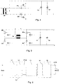
- FIG. 4 shows the use of two semiconductor switch units DS with buffer capacitors C in a known center-point rectifier.
- the AC voltage is coupled via a transformer with a primary winding and two symmetrical secondary windings.
- By rectifying a pulsating DC voltage is generated, which is smoothed by an electrolytic capacitor C2.
- the smaller capacitor C1 serves to suppress interfering harmonics.
- FIG. 5 shows the use of four semiconductor switch units DS with buffer capacitors C in a bridge rectifier known per se.
- the AC voltage is coupled via a transformer with a primary winding and a secondary windings, the latter lying in a bridge branch of the rectifier bridge formed by the four semiconductor switch units DS.
- By rectifying a pulsating DC voltage is generated, which is smoothed by an electrolytic capacitor C2.
- the smaller capacitor C1 serves to suppress interfering harmonics.
- FIG. 6 shows a per se known ballast 10 for operating at least one LED, OLED or DC halogen lamp or other DC-supplied light source starting from an AC voltage, eg. A mains voltage.
- the mains voltage is rectified in a first rectifier circuit part 12.
- the first rectifier circuit part 12 is still provided with an actively clocked PFC stage, which in turn ensures that the current drawn from the network is sinusoidal as possible.
- the first rectifier circuit part 12 generates a DC voltage Ubus regulated by the PFC stage. This is in a DC / AC converter 13 with transformer, which also provides a potential separation, again converted into an AC voltage whose voltage value is considerably less than that of the mains voltage and thus adjusted to the operating voltage value of the LED. Accordingly, the current is transformed up.
- the AC voltage thus generated is rectified again in a second rectifier circuit part 14.
- This second rectifier stage 14 must process small voltages but high currents.
- the use of the semiconductor switch units DS described above lends itself.
- the output voltage of the second rectifier stage 14 can be further processed, for example. Modulated, in particular PWM-modulated, before being supplied to the bulbs.
- the lighting means are thus supplied generally starting from the output voltage of the second rectifier stage 14.
Landscapes
- Engineering & Computer Science (AREA)
- Power Engineering (AREA)
- Circuit Arrangement For Electric Light Sources In General (AREA)
- Rectifiers (AREA)
- Dc-Dc Converters (AREA)
Description
- Die Erfindung betrifft Betriebsgeräte für Leuchtmittel. Die Erfindung kann Anwendung finden bspw. in Betriebsgeräten ("Konvertern") für OLEDs, LEDs, oder DC-Halogenlampen.
- Bekanntlich fällt über Dioden im Durchlass eine nicht unbeachtliche Durchflussspannung von beispielsweise 0,8V ab. Bei kleinen Ausgangsspannungen und entsprechend hohen Strömen entstehen dadurch beachtliche Gleichrichtungsverluste. So liegen die Verluste bei einem Mittelpunktsgleichrichter (2 Dioden) für einen 100W Konverter mit 8A bspw. bei etwa 6,4W. An einem 10 mOhm-Widerstand entsteht im Vergleich dazu bei einem Strom von 8A nur eine Verlustleistung von 0,64W.
- Es ist bereits aus der
DE 10012362A1 bekannt, zur Gleichrichtung von Wechselspannungen anstelle von Dioden elektronische Schalterelemente zu verwenden, die im Rhythmus der Wechselspannung so gesteuert werden, dass sie in der einen Polaritätsphase leitend und in der anderen nichtleitend sind. Bei derartig aktiv gesteuerten Schalterelementen ist es jedoch schwierig, allein durch Auswertung der gleichzurichtenden Wechselspannung die genauen Umschaltzeitpunkte zu bestimmen. -
US6992906 A1 ,US6535400 B2 undEP1148624 A1 stellen weiteren Stand der Technik für die vorliegende Anmeldung dar. - Der Erfindung liegt daher die Aufgabe zugrunde, ein Verfahren und eine Schaltungsanordnung zum Gleichrichten einer Wechselspannung anzugeben, das/die weiterhin mit Dioden arbeitet, bei dem/der aber die Vorwärtsverluste der Dioden signifikant reduziert werden können.
- Die Aufgabe wird gelöst durch die Merkmale der unabhängigen Ansprüche. Die abhängigen Ansprüche betreffen zweckmäßige Ausgestaltungen der Erfindung.
- Ein erster Aspekt betrifft ein Betriebsgerät für Leuchtmittel, insbesondere LEDs, OLEDs oder Halogenlampen, aufweisend eine Schaltungsanordnung zum Gleichrichten einer Wechselspannung mit mindestens einer Diode (D1), wobei zu der Diode ein durch ein elektronisches Schalterelement parallel geschaltet ist, das einen geringeren Durchlasswiderstand als die Diode hat, und dass Steuermittel für das Schalterelement vorgesehen sind, die gewährleisten, dass die Durchlassdauer des Schalterelementes innerhalb derjenigen der Diode liegt.
- Die Steuermittel können ferner gewährleisten, dass die Durchlassdauer des Schalterelementes früher als diejenige der Diode endet.
- Die Steuermittel können das Schalterelement so steuern, dass die Durchlassdauer des Schalterelementes unter Auswertung der vorangegangenen Sperrperioden der Diode dynamisch adaptiert wird.
- Die Steuermittel können das Schalterelement so steuern, dass die Durchlassdauer für das Schalterelement zunächst kurz im Vergleich zu der Durchlassdauer der Diodebemessen ist und dann sukzessive erhöht wird,
und dass die Durchlassdauer für das Schalterelement wieder verkürzt wird, wenn diese später als die Durchlasszeit der Diode endet. - Die Steuermittel können einen Schaltregler aufweisen, der die Spannung über der Diode direkt oder indirekt misst und sie für die Steuerung des Schalterelementes auswertet.
- Die Steuermittel können die Serienschaltung aus einem Vorwiderstand, einer weiteren Diode und einem Puffer-Kondensator aufweisen, die zu dem Schalterelement parallel geschaltet ist. Der der Schaltregler einerseits mit dem Verbindungspunkt zwischen dem Vorwiderstand und der weiteren Diode und andererseits mit dem Verbindungspunkt zwischen dem Puffer-Kondensator und dem Schalterelement verbunden ist.
- Das Schalterelement kann ein Feldeffekttransistor sein, dessen Source-Anschluss mit dem einen Anschluss der erstgenannten Diode verbunden ist, dessen Drain-Anschluss mit dem anderen Anschluss der erstgenannten Diode verbunden ist, und dessen Gate-Anschluss mit dem SteuerAusgang des Schaltreglers verbunden ist.
- Die erstgenannte Diode kann dabei die Body-Diode des Feldeffekttransistors sein.
- Die erstgenannte Diode, das Schalterelement, der Vorwiderstand, die weitere Diode und der Schaltregler können zu einer integrierten Halbleiter-Schaltereinheit gehören,
und dass der Puffer-Kondensator in Bezug auf die Halbleiter-Schaltereinheit ein externes Bauelement ist. - In dem Betriebsgerät können integrierte Halbleiter-Schaltereinheiten in einem Mittelpunktsgleichrichter oder in einem Brückengleichrichter mit Einkopplung der Wechselspannung über einen Transformator verwendet werden.
- Ein weiterer Aspekt betrifft ein Betriebsgerät für mindestens ein Leuchtmittel, insbesondere eine LED,
wobei eine Netzspannung zunächst in einer ersten Gleichrichter-Stufe gleichgerichtet wird,
wobei dann die so erzeugte Gleichspannung in einem DC/AC-Wandler wieder in eine Wechselspannung höherer Frequenz als die der Netzspannung umgewandelt wird,
wobei der Spannungswert der so erzeugten Wechselspannung höherer Frequenz transformatorisch reduziert wird,
wobei die transformatorisch reduzierte Wechselspannung in einer zweiten Gleichrichterstufe erneut zur Versorgung der mindestens einen LED gleichgerichtet wird, und wobei die integrierten Halbleiter-Schaltereinheiten zumindest in der zweiten Gleichrichterstufe eingesetzt sind. - Der Grundgedanke der Erfindung besteht also darin, eine Diode mit einem zu dieser parallel geschalteten aktiv steuerbaren Schalterelement zu kombinieren, das einen geringeren Durchlasswiderstand als die Diode hat. Das Schalterelement wird dann so gesteuert, dass es - wenn die Diode in den Durchlasszustand übergegangen ist - den Durchlassstrom weitgehend übernimmt.
- Die Kombination von aktiv gesteuertem Schalterelement mit einer Diode erlaubt es auch, die oben erwähnte Schwierigkeit zu überwinden, die genauen Umschaltzeitpunkte für das Schalterelement bestimmen zu können. Letztere werden nunmehr anhand der messbaren Umschaltung der Diode bzw. unter Auswertung der Historie der Sperrperioden der Diode bestimmt.
- Vorzugsweise wird die Einschaltdauer für das Schalterelement kürzer als die der Diode gewählt, was erlaubt, sie später beginnen und/oder früher enden zu lassen.
- Zweckmäßigerweise wird die Durchlassdauer des Schalterelementes dynamisch adaptiert, in der Weise, dass das Schalterelement immer in den Sperrzustand umgeschaltet wird, bevor der Stromfluss durch dieses Null wird oder seine Polarität wechselt.
- Beim Umschalten des Schalterelementes vom Sperrzustand auf Durchlass kann man zur Realisierung der gewünschten Einschaltverzögerung gegenüber der Diode die technisch bedingte Verzögerung ausnutzen, die bei dem Schalterelement natürlicherweise zwischen der Ausgabe des Umschaltsignals und dem tatsächlichen Umschalten auftritt. Das Umschaltsignal wird dann ausgegeben, wenn festgestellt wird, dass die Diode vom Sperrzustand in den Durchlasszustand übergeht.
- Für die Bestimmung des Zeitpunktes des Umschaltens des Schalterelementes vom Durchlasszustand in den Sperrzustand gibt es mehrere Möglichkeiten. Eine erste Möglichkeit ist die, die Frequenz bzw. zeitliche Taktung eines zurückliegenden Ein-/Aus-Zyklus zu erfassen, auszuwerten und das Umschaltsignal für die nächste Umschaltung des Schalterelementes mit einer Sicherheitsmarge zu beaufschlagen. Wenn sich die Frequenz der gleichzurichtenden Wechselspannung in relativ kleinen (inkrementellen) Schritten ändert, so gewährleistet die Sicherheitsmarge, dass das Schalterelement immer zeitlich vor der Diode in den Sperrzustand übergeht.
- Was die Schaltungsanordnung betrifft, so erlaubt es die Erfindung, eine neuartige Halbleiter-Schaltereinheit zu kreieren, die sich dadurch auszeichnet, dass das Schalterelement und die Diode in diesem integriert sind. Bei Ausbildung des Schalterelementes als Feldeffekttransistor kann die Diode dessen Body-Diode sein.
- Eine solche Halbleiter-Schaltereinheit kann ferner einen - ebenfalls integrierten - Schaltregler enthalten, der die aktuelle Spannung über der Diode auswertet, um die Umschaltsignale für das Schalterelement zu erzeugen. Die Energie zum Betreiben des Schaltreglers und zum Erzeugen der Umschaltsignale können durch zusätzliche Gleichrichtung aus der gleichzurichtenden Gleichspannung gewonnen werden. Die durch diese zusätzliche Gleichrichtung gewonnene Arbeitsspannung kann in einem Puffer-Kondensator gespeichert werden, der vorzugsweise in Bezug auf die integrierte Halbleiter-Schaltereinheit als externes Bauelement ausgeführt ist.
- Halbleiter-Schaltereinheiten der vorstehend angegebenen Art können in den verschiedensten Schaltungsanordnungen zur Gleichrichtung von Wechselspannungen Anwendung finden, bei denen eine Gleichrichter-Diode vorgesehen ist (beispielsweise in AC/DC-Wandlern, Flyback-Konvertern usw.). Es versteht sich, dass sie sich insbesondere dort für einen Einsatz empfehlen, wo kleine Spannungen und hohe Ströme auftreten, beispielsweise in Vorschaltgeräten zum Betreiben von LEDs, wobei die Spannungsquelle das Netz ist.
- Wenn derartige Halbleiter-Schaltereinheiten in mehrfacher Zahl beispielsweise in Mittelpunkts-Gleichrichtern oder Brückengleichrichtern eingesetzt werden, so empfiehlt es sich die Ansteuerung der einzelnen Halbleiter-Schaltereinheiten aufeinander abzustimmen bzw. zu synchronisieren, indem die Messergebnisse der Schaltregler simultan ausgewertet werden oder indem man die Halbleiter-Schaltereinheiten miteinander kommunizieren lässt. Dies alles mit dem Ziel, die Halbleiter-Schaltereinheiten innerhalb des Gesamtverbunds "sanft" zu- oder wegzuschalten.
- Ausführungsbeispiele der Erfindung werden nachfolgend anhand der Zeichnungen beschrieben.
- Es zeigen:
-
Figur 1 eine erfindungsgemäße Halbleiter-Schaltereinheit; -
Figur 2 die Halbleiter-Schaltereinheit gemäßFigur 1 als eigenständiges Schaltsymbol; -
Figur 3 eine Darstellung der durch den Schaltregler gemessenen Spannung VSense in Abhängigkeit von der Zeit; -
Figur 4 einen üblichen Mittelpunktsgleichrichter, hier allerdings unter Verwendung von Halbleiter-Schaltereinheiten gemäßFigur 1 bzw.Figur 2 ; -
Figur 5 einen üblichen Brückengleichrichter, hier allerdings unter Verwendung von Halbleiter-Schaltereinheiten gemäßFigur 1 bzw.Figur 2 ; -
Figur 6 ein mit Wechselspannung, insbesondere Netzspannung zu betreibendes Vorschaltgerät für eine oder mehrere LEDs, OLEDs oder DC-Halogenlampen, wobei das Vorschaltgerät zur Gleichrichtung Halbleiter-Schaltereinheiten gemäßFigur 1 bzw.Figur 2 verwendet. - In
Figur 1 befindet sich eine zur Gleichrichtung einer Wechselspannung bestimmte erste Diode D1 in einer die Wechselspannung führenden Leitung. Parallel zu der ersten Diode D1 liegt ein elektronisches Schalterelement S in Form eines MOS-FETs, wobei die Diode D1 die Body-Diode des MOS-FETs sein kann. Der Source-Anschluss des MOS-FETs ist mit dem einen Anschluss der Diode D1 und der Drain-Anschluss des MOS-FETS ist mit dem anderen Anschluss der Diode D1 verbunden. Der Gate- Anschluss des MOS-FETs ist mit dem Steuersignal-Ausgang eines Schaltreglers 1 verbunden. Dieser wird über eine Serienschaltung aus einem Vorwiderstand R1, einer weiteren Diode D2 und einem Puffer-Kondensator C mit Spannung versorgt. Dazu ist der eine Endpunkt der Serienschaltung mit dem einen Anschluss und der andere Endpunkt der Serienschaltung mit dem anderen Anschluss der ersten Diode D1 verbunden. Der Schaltregler 1 greift die für ihn bestimmte Versorgungsgleichspannung VCC an dem Puffer-Kondensator C ab. Die Versorgungsgleichspannung VCC wird mittels des Vorwiderstandes R1 und der weiteren Diode D2 durch Gleichrichtung der gleichzurichtenden Wechselspannung gewonnen und in dem Puffer-Kondensator C gespeichert. - Der Schaltregler 1 tastet an dem Verbindungspunkt zwischen dem Vorwiderstand R1 und der weiteren D2 die Spannung VSense ab, die der über der ersten Diode D1 abfallenden Spannung entspricht und Informationen darüber liefert, wann die Diode D1 leitend bzw. nichtleitend wird.
- Die erste Diode D1, das Schalterelement S, der Schaltregler 1, der Vorwiderstand R1 und die zweite Diode D2 bilden eine integriertes Halbleiter-Schaltereinheit DS bzw. sind integrierte Teile desselben. Der Puffer-Kondensator C ist in Bezug auf die integrierte Halbleiter-Schaltereinheit DS ein externes Bauelement.
- In
Figur 2 ist die Halbleiter-Schaltereinheit als eigenständiges Schaltsymbol mit drei Anschlüssen dargestellt, dass in den nachfolgend beschriebenen Schaltungsanordnungen verwendet ist. - Die Steuerung des Schalterelementes S durch den Schaltregler 1 wird nachfolgend anhand der in
Figur 3 dargestellten zeitlichen Spannungsverläufe beschrieben. -
Figur 3 zeigt die von dem Schaltregler 1 gegen Masse GND gemessene Spannung VSense. Diese zeigt, dass über der Diode 1 wechselweise eine Spannung zwischen -48V und +0,8V abfällt. Wenn die an der Diode D1 liegende Wechselspannung kleiner als +0,8V ist, sperrt die Diode. Wenn die Wechselspannung dagegen über +0,8V ansteigt, wird die Diode D1 leitend, wobei der Spannungsabfall über der Diode D1 auch dann nicht unter +0,8V sinkt, wenn die gleichzurichtende Wechselspannung einen Spannungswert von über +0,8V annimmt. Das hat zur Folge, dass an der Diode D1 im Durchlasszustand eine beachtliche Verlustleistung entsteht, die sich aus dem dem Produkt des durch die Diode D1 fließenden Stromes und der Durchflussspannung von 0,8V ergibt. Wie eingangs beschrieben, kann diese Verlustleistung beachtlich sein und ist in jedem Fall unerwünscht. - Um die Verlustleistung zu reduzieren, wurde zu der Diode D1 ein Schalterelement S parallel geschaltet, das über dem im Durchlass-Zustand eine wesentlich geringere Durchflussspannung abfällt, als an der Diode D1. Das ist gleich bedeutend damit, dass der Durchlasswiderstand des Schalterelementes S wesentlich geringer ist als der der Diode D1. Der Unterschied zwischen den Durchflussspannungen ist in
Figur 3 mit Vred bezeichnet. Die Reduzierung der Verlustleistung ergibt sich als Produkt aus Vred und dem durch die Kombination aus der Diode D1 und dem Schalterelement S fließenden Strom. - Das Schalterelement S wird nun so gesteuert, dass seine Durchlassdauer ton innerhalb der Durchlassdauer Ton der Diode D1 liegt. D.h. die Durchlassdauer des Schaltelements beginnt frühestens und endet spätestens mit der Durchlassdauer der Diode, kann aber auch später beginnen und/oder früher enden.
- Im Ausführungsbeispiel beginnt die Durchlassdauer ton des Schalterelementes S um die Verzögerungszeit t1 später als die Durchlassdauer Ton der Diode D1 und endet um die Margenzeit t2 früher als diese.
- Es versteht sich, dass die Verzögerungszeit t1 und die Margenzeit t2 möglichst kurz sein sollten (idealerweise 0, Schaltzeiten mitgerechnet). Sie sind aber notwendig, um zu gewährleisten, dass das Schalterelement S den wesentlichen Stromfluss nur dann übernimmt, wenn die Diode sicher leitend ist. Es ist insbesondere wichtig, dass das Schalterelement S im leitenden Zustand noch vor dem Zeitpunkt deaktiviert wird, an dem der Strom Null wird oder die Polarität wechselt. Auf diese Weise wird gewährleistet, dass der Stromfluss zum Ende eines Gleichrichterzyklus wieder über die Diode erfolgt, die ein natürliches Gleichrichterverhalten aufweist. Damit wird auch erreicht, dass das Schalterelement S sicher in den Sperrzustand übergeht bzw. dass der Kanal in dem das Schalterelement S bildenden Halbleiter wieder vollkommen sperrt.
- Die Bestimmung der einzelnen Schaltzeitpunkte für das Schalterelement S kann auf mindestens zwei verschiedene Weisen erfolgen.
- Bei Gleichrichtersystemen mit einem Tastverhältnis von 50% (beispielsweise bei Netzgleichrichtung) bestimmt der Schaltregler 1 den Einschaltzeitpunkt für den Beginn der Durchlasszeit des Schalterelementes S indem er - verzögert um t1 - dann ein Einschaltsignal abgibt, wenn die Messspannung VSense gegen Masse GND Null wird oder die Polarität wechselt. Die Durchlassdauer ton für das Schalterelement S legt der Schaltregler 1 dann aufgrund der ebenfalls über VSense erfolgenden Überwachung und Auswertung der vorangegangenen Durchlassperioden Ton der Diode D1 fest.
- Bei PWM-Systemen wird ebenfalls die Historie der vorangegangenen Umschaltvorgänge der Diode D1 ausgewertet. Der Schaltregler 1 deaktiviert dazu das Schalterelement S für einige Zyklen. Danach schaltet er das Schalterelement 1 nur mit einer sehr kurzen Zeitspanne ton auf Durchlass und erhöht ton dann sukzessive mit jedem Zyklus. Dies wird solange fortgesetzt, wie über VSense noch ein Spannungsanstieg am Ende von ton feststellbar ist. Wenn das nicht mehr der Fall ist, wird die Durchlasszeit ton für das Schalterelement S wieder reduziert bis wieder ein Spannungsanstieg messbar ist.
-
Figur 4 zeigt den Einsatz von zwei Halbleiter-Schaltereinheiten DS mit Puffer-Kondensatoren C in einem an sich bekannten Mittelpunkts-Gleichrichter. Die Wechselspannung wird über einen Transformator mir einer Primärwicklung und zwei symmetrischen Sekundärwicklungen eingekoppelt. Durch die Gleichrichtung wird eine pulsierende Gleichspannung erzeugt, die durch einen Elektrolytkondensator C2 geglättet wird. Der kleinere Kondensator C1 dient zur Unterdrückung von störenden Oberwellen. -
Figur 5 zeigt den Einsatz von vier Halbleiter-Schaltereinheiten DS mit Puffer-Kondensatoren C in einem an sich bekannten Brücken-Gleichrichter. Die Wechselspannung wird über einen Transformator mir einer Primärwicklung und einer Sekundärwicklungen eingekoppelt, wobei letztere in einem Brückenzweig der von den vier Halbleiter-Schalter-Einheiten DS gebildeten GleichrichterBrücke liegt. Durch die Gleichrichtung wird eine pulsierende Gleichspannung erzeugt, die durch einen Elektrolytkondensator C2 geglättet wird. Der kleinere Kondensator C1 dient zur Unterdrückung von störenden Oberwellen. -
Figur 6 zeigt ein an sich bekanntes Vorschaltgerät 10 zum Betreiben mindestens einer LED, OLED oder DC-Halogenlampe oder anderer DC versorgter Leuchtmittel ausgehend von einer Wechselspannung, bspw. einer Netzspannung. Die Netzspannung wird in einem ersten Gleichrichter-Schaltungsteil 12 gleichgerichtet. Zur Vermeidung der Rückstrahlung von bei der Gleichrichtung entstehenden unerwünschten Oberwellen in das Netz ist zwischen den ersten Gleichrichter-Schaltungsteil 12 und dem Netzeingang noch eine Oberwellenfilter eingefügt. Darüber hinaus ist der erste Gleichrichter-Schaltungsteil 12 noch mit einer aktiv getakteten PFC-Stufe versehen, die ihrerseits dafür sorgt, dass der dem Netz entnommene Strom möglichst sinusförmig ist. - Der erste Gleichrichter-Schaltungsteil 12 erzeugt eine durch die PFC-Stufe geregelte Gleichspannung Ubus. Diese wird in einem DC/AC-Wandler 13 mit Transformator, der auch für eine Potentialtrennung sorgt, wieder in eine Wechselspannung umgeformt, deren Spannungswert erheblich geringer als derjenige der Netzspannung und damit an den Betriebsspannungswert der LED angeglichen ist. Entsprechend wird der Strom hochtransformiert.
- Die so erzeugte Wechselspannung wird in einem zweiten Gleichrichter-Schaltungsteil 14 erneut gleichgerichtet. Diese zweite Gleichrichter-Stufe 14 muss kleine Spannungen, aber hohe Ströme verarbeiten. Hier bietet sich der Einsatz der oben beschriebenen Halbleiter-Schaltereinheiten DS an.
- Die Ausgangsspannung der zweiten Gleichrichter-Stufe 14 kann noch weiter aufbereitet, bspw. moduliert, insbesondere PWM-moduliert werden, bevor sie den Leuchtmitteln zugeführt wird. Die Leuchtmittel werden also allgemein ausgehend von der Ausgangsspannung der zweiten Gleichrichter-Stufe 14 versorgt.
- In einer letzten Stufe 15 erfolgt eine weitere Filterung auf Oberwellen sowie eine Anpassung an den Strombedarf der mit dem Vorschaltgerät zu betreibenden LED durch eine entsprechende Regelschaltung.
Claims (6)
- Betriebsgerät für Leuchtmittel, insbesondere LEDs, OLEDs oder Halogenlampen,
aufweisend:- einen DC/AC-Wandler mit Transformator zur Bereitstellung einer Wechselspannung, und- eine Schaltungsanordnung zum Gleichrichten der Wechselspannung mit mindestens einer Diode (D1),wobei zu der Diode (D1) ein elektronisches Schalterelement (S) parallel geschaltet ist, das einen geringeren Durchlasswiderstand als die Diode (D1) hat,
und Steuermittel für das Schalterelement (S) vorgesehen sind, die gewährleisten, dass die Durchlassdauer (ton) des Schalterelementes (S) innerhalb derjenigen (Ton) der Diode (D1) liegt, wobei das Steuermittel ein Schaltregler (1) ist, der eine Spannung (VSense), die der über der ersten Diode (D1) abfallenden Spannung entspricht, an einem Verbindungspunkt zwischen einem Vorwiderstand (R1) und einer weiteren Diode (D2) erfasst und auswertet und abhängig davon Umschaltsignale für das Schalterelement (S) erzeugt,
wobei der Schaltregler (1) über eine Serienschaltung aus dem Vorwiderstand (R1), der weiteren Diode (D2) und einem Puffer-Kondensator (C) mit Spannung versorgt ist,
wobei die Serienschaltung zu dem Schalterelement (S) parallel geschaltet ist, und
wobei die Steuermittel das Schalterelement (S) so steuern, dass die Durchlassdauer (ton) für das Schalterelement (S) zunächst kurz im Vergleich zu der Durchlassdauer (Ton) der Diode (D1) bemessen ist und dann sukzessive erhöht wird,
und dass die Durchlassdauer (ton) für das Schalterelement (S) wieder verkürzt wird, wenn diese später als die Durchlasszeit (Ton) der Diode (S) endet. - Betriebsgerät nach Anspruch 1,
dadurch gekennzeichnet,
dass zu den Steuermitteln die Serienschaltung aus dem Vorwiderstand (R1), der weiteren Diode (D2) und dem Puffer-Kondensator (C) gehört, die zu dem Schalterelement (S) parallel geschaltet ist,
dass der Schaltregler (1) einerseits mit dem Verbindungspunkt zwischen dem Vorwiderstand (R1) und der weiteren Diode (D2) und andererseits mit dem Verbindungspunkt zwischen dem Puffer-Kondensator (C) und dem Schalterelement (S) verbunden ist. - Betriebsgerät nach Anspruch 2,
dadurch gekennzeichnet,
dass das Schalterelement (S) ein Feldeffekttransistor ist, dessen Source-Anschluss mit dem einen Anschluss der erstgenannten Diode (D1) verbunden ist, dessen Drain-Anschluss mit dem anderen Anschluss der erstgenannten Diode (D1) verbunden ist, und dessen Gate-Anschluss mit dem SteuerAusgang des Schaltreglers (1) verbunden ist. - Betriebsgerät nach Anspruch 3,
dadurch gekennzeichnet,
dass die erstgenannte Diode die Body-Diode des Feldeffekttransistors ist - Betriebsgerät nach einem der Ansprüche 2 bis 4,
dadurch gekennzeichnet,
dass die erstgenannte Diode (D1), das Schalterelement (S), der Vorwiderstand (R1), die weitere Diode (D2) und der Schaltregler (S) zu einer integrierten Halbleiter-Schaltereinheit (DS) gehören,
und dass der Puffer-Kondensator (C) in Bezug auf die Halbleiter-Schaltereinheit (1) ein externes Bauelement ist. - Betriebsgerät nach einem der vorhergehenden Ansprüche, bei dem integrierte Halbleiter-Schaltereinheiten (DS) in einem Mittelpunkt-Gleichrichter oder in einem Brückengleichrichter mit Einkopplung der Wechselspannung über einen Transformator verwendet werden.
Applications Claiming Priority (2)
| Application Number | Priority Date | Filing Date | Title |
|---|---|---|---|
| DE102009041515A DE102009041515A1 (de) | 2009-09-14 | 2009-09-14 | Verfahren und Schaltungsanordnung zum Gleichrichten einer Wechselspannung |
| PCT/EP2010/063457 WO2011029953A1 (de) | 2009-09-14 | 2010-09-14 | Betriebsgerät für leuchtmittel |
Publications (2)
| Publication Number | Publication Date |
|---|---|
| EP2478629A1 EP2478629A1 (de) | 2012-07-25 |
| EP2478629B1 true EP2478629B1 (de) | 2018-06-13 |
Family
ID=43413798
Family Applications (1)
| Application Number | Title | Priority Date | Filing Date |
|---|---|---|---|
| EP10751969.6A Not-in-force EP2478629B1 (de) | 2009-09-14 | 2010-09-14 | Betriebsgerät für leuchtmittel |
Country Status (4)
| Country | Link |
|---|---|
| EP (1) | EP2478629B1 (de) |
| CN (1) | CN102577064B (de) |
| DE (1) | DE102009041515A1 (de) |
| WO (1) | WO2011029953A1 (de) |
Families Citing this family (2)
| Publication number | Priority date | Publication date | Assignee | Title |
|---|---|---|---|---|
| CN103944426B (zh) * | 2014-05-05 | 2017-08-08 | 广州金升阳科技有限公司 | 一种同步整流实现方法 |
| CN104582169B (zh) * | 2014-12-29 | 2017-03-15 | 浙江欧易新能源有限公司 | 一种变色温led光源的控制装置 |
Citations (6)
| Publication number | Priority date | Publication date | Assignee | Title |
|---|---|---|---|---|
| DE19946025A1 (de) * | 1999-09-25 | 2001-03-29 | Bosch Gmbh Robert | Vorrichtung zur Stromversorgung einer Ansteuerschaltung für ein getaktetes Schaltnetzteil |
| EP1148624A1 (de) * | 2000-04-10 | 2001-10-24 | STMicroelectronics S.r.l. | Verfahren und Vorrichtung zur digitaler Kontrolle der Ausschaltzeit der Synchrongleichrichter für Schaltnetzteile mit isolierten Topologien |
| US6535400B2 (en) * | 2001-03-30 | 2003-03-18 | Texas Instruments Incorporated | Control circuit for synchronous rectifiers in DC/DC converters to reduce body diode conduction losses |
| US20030193364A1 (en) * | 2002-04-16 | 2003-10-16 | Liu Kwang H. | Biasing system and method for low voltage DC-DC converters with built-in N-FETs |
| US6992906B1 (en) * | 2002-12-10 | 2006-01-31 | Edward Herbert | Synthetic rectifiers |
| US7196914B2 (en) * | 2004-11-19 | 2007-03-27 | Virginia Tech Intellectual Properties, Inc. | Power converters having capacitor resonant with transformer leakage inductance |
Family Cites Families (6)
| Publication number | Priority date | Publication date | Assignee | Title |
|---|---|---|---|---|
| US4924109A (en) * | 1987-11-02 | 1990-05-08 | Weber Harold J | Dim-down electric light time switch method and apparatus |
| DE20024005U1 (de) | 2000-03-14 | 2009-05-20 | Tridonicatco Gmbh & Co. Kg | Elektronischer Transformator |
| JP3624186B2 (ja) * | 2002-03-15 | 2005-03-02 | Tdk株式会社 | スイッチング電源装置用の制御回路及びこれを用いたスイッチング電源装置 |
| WO2005013468A1 (en) * | 2003-08-01 | 2005-02-10 | Philips Intellectual Property & Standards Gmbh | Output voltage control of a synchronous rectifier |
| DE10345929A1 (de) * | 2003-10-02 | 2005-04-21 | Bosch Gmbh Robert | Elektronischer Diodenschaltkreis |
| US7746042B2 (en) * | 2006-10-05 | 2010-06-29 | Advanced Analogic Technologies, Inc. | Low-noise DC/DC converter with controlled diode conduction |
-
2009
- 2009-09-14 DE DE102009041515A patent/DE102009041515A1/de not_active Withdrawn
-
2010
- 2010-09-14 CN CN201080040875.4A patent/CN102577064B/zh not_active Expired - Fee Related
- 2010-09-14 WO PCT/EP2010/063457 patent/WO2011029953A1/de not_active Ceased
- 2010-09-14 EP EP10751969.6A patent/EP2478629B1/de not_active Not-in-force
Patent Citations (6)
| Publication number | Priority date | Publication date | Assignee | Title |
|---|---|---|---|---|
| DE19946025A1 (de) * | 1999-09-25 | 2001-03-29 | Bosch Gmbh Robert | Vorrichtung zur Stromversorgung einer Ansteuerschaltung für ein getaktetes Schaltnetzteil |
| EP1148624A1 (de) * | 2000-04-10 | 2001-10-24 | STMicroelectronics S.r.l. | Verfahren und Vorrichtung zur digitaler Kontrolle der Ausschaltzeit der Synchrongleichrichter für Schaltnetzteile mit isolierten Topologien |
| US6535400B2 (en) * | 2001-03-30 | 2003-03-18 | Texas Instruments Incorporated | Control circuit for synchronous rectifiers in DC/DC converters to reduce body diode conduction losses |
| US20030193364A1 (en) * | 2002-04-16 | 2003-10-16 | Liu Kwang H. | Biasing system and method for low voltage DC-DC converters with built-in N-FETs |
| US6992906B1 (en) * | 2002-12-10 | 2006-01-31 | Edward Herbert | Synthetic rectifiers |
| US7196914B2 (en) * | 2004-11-19 | 2007-03-27 | Virginia Tech Intellectual Properties, Inc. | Power converters having capacitor resonant with transformer leakage inductance |
Also Published As
| Publication number | Publication date |
|---|---|
| WO2011029953A1 (de) | 2011-03-17 |
| CN102577064B (zh) | 2014-10-29 |
| DE102009041515A1 (de) | 2011-03-24 |
| EP2478629A1 (de) | 2012-07-25 |
| CN102577064A (zh) | 2012-07-11 |
Similar Documents
| Publication | Publication Date | Title |
|---|---|---|
| DE102015105488A1 (de) | System und verfahren für eine getaktete leistungsversorgung | |
| EP3350911B1 (de) | Pfc-modul für lückenden betrieb | |
| EP2837263A2 (de) | Verfahren zum steuern einer leistungsfaktorkorrekturschaltung, leistungsfaktorkorrekturschaltung und betriebsgerät für ein leuchtmittel | |
| EP3202235B1 (de) | Getakteter elektronischer energiewandler mit einstellbarer lückenzeit | |
| DE102017115474A1 (de) | System und Verfahren zum Steuern von Strom in einem Schaltregler | |
| DE102015118658A1 (de) | Sekundärseitige Steuerung von Resonanz-DC/DC-Wandlern | |
| EP3114898B1 (de) | Led-treiber | |
| DE102018126317B4 (de) | LED-Treiber und Ansteuerverfahren | |
| DE112012006360T5 (de) | Gleichstromversorgungskreis | |
| DE102012224212A1 (de) | Primärseitig gesteuerter Konstantstrom-Konverter für Beleuchtungseinrichtungen | |
| EP2478629A1 (de) | Betriebsgerät für leuchtmittel | |
| DE102017100427A1 (de) | Gleichstromversorgungsvorrichtung und Lichtsystem, das diese verwendet | |
| DE102014223377B4 (de) | Betriebsschaltung zur Versorgung eines Leuchtmittels, LED-Konverter, System und Verfahren zum Betreiben einer Betriebsschaltung | |
| AT15390U1 (de) | Verfahren zur Regelung eines LED-Moduls | |
| AT17184U1 (de) | Konverterschaltung für Leuchtmittel mit einem Messpunkt zur Erfassung kombinierter elektrischer Parameter | |
| DE102014221024A1 (de) | Betriebsschaltung für Leuchtmittel mit PFC-Steuereinheit | |
| EP3815469B1 (de) | Synchrone sperrwandlerschaltung zum betrieb einer leuchtmittelstrecke | |
| DE102014215835B4 (de) | LED Konverter, Verfahren zum Versorgen eines LED Strangs, Betätigungsvorrichtung mit dem LED Konverter, sowie LED Leuchte mit dem LED Konverter | |
| DE102015208774B4 (de) | Vorrichtung mit getaktetem Wandler zum Betrieb von Leuchtmitteln und Leuchte mit einer solchen Verwendung | |
| DE102020103921B4 (de) | Betriebsvorrichtung und Verfahren zum Betreiben einer Leuchtmittelanordnung | |
| AT16905U1 (de) | Schaltwandler mit zyklischer Frequenzänderung | |
| DE202017103713U1 (de) | Einstufige Konverterschaltungsanordnung mit Linearregler | |
| DE102007047725A1 (de) | Direkte Stromlieferung mit einem induktiven Abwärts- oder Aufwärtswandler zur Anwendung auf LED-Treiber | |
| DE102013105463B3 (de) | Betriebsvorrichtung und Verfahren zum Betreiben einer dimmbaren Leuchtmittelanordnung | |
| AT17617U1 (de) | Schaltungsanordnung zum Betreiben von Leuchtmitteln |
Legal Events
| Date | Code | Title | Description |
|---|---|---|---|
| PUAI | Public reference made under article 153(3) epc to a published international application that has entered the european phase |
Free format text: ORIGINAL CODE: 0009012 |
|
| 17P | Request for examination filed |
Effective date: 20120227 |
|
| AK | Designated contracting states |
Kind code of ref document: A1 Designated state(s): AL AT BE BG CH CY CZ DE DK EE ES FI FR GB GR HR HU IE IS IT LI LT LU LV MC MK MT NL NO PL PT RO SE SI SK SM TR |
|
| DAX | Request for extension of the european patent (deleted) | ||
| 17Q | First examination report despatched |
Effective date: 20140620 |
|
| STAA | Information on the status of an ep patent application or granted ep patent |
Free format text: STATUS: EXAMINATION IS IN PROGRESS |
|
| REG | Reference to a national code |
Ref country code: DE Ref legal event code: R079 Ref document number: 502010015077 Country of ref document: DE Free format text: PREVIOUS MAIN CLASS: H02M0003158000 Ipc: H05B0033080000 |
|
| GRAP | Despatch of communication of intention to grant a patent |
Free format text: ORIGINAL CODE: EPIDOSNIGR1 |
|
| STAA | Information on the status of an ep patent application or granted ep patent |
Free format text: STATUS: GRANT OF PATENT IS INTENDED |
|
| RIC1 | Information provided on ipc code assigned before grant |
Ipc: H05B 33/08 20060101AFI20180316BHEP Ipc: H02M 3/158 20060101ALI20180316BHEP |
|
| INTG | Intention to grant announced |
Effective date: 20180404 |
|
| GRAS | Grant fee paid |
Free format text: ORIGINAL CODE: EPIDOSNIGR3 |
|
| GRAA | (expected) grant |
Free format text: ORIGINAL CODE: 0009210 |
|
| STAA | Information on the status of an ep patent application or granted ep patent |
Free format text: STATUS: THE PATENT HAS BEEN GRANTED |
|
| AK | Designated contracting states |
Kind code of ref document: B1 Designated state(s): AL AT BE BG CH CY CZ DE DK EE ES FI FR GB GR HR HU IE IS IT LI LT LU LV MC MK MT NL NO PL PT RO SE SI SK SM TR |
|
| REG | Reference to a national code |
Ref country code: GB Ref legal event code: FG4D Free format text: NOT ENGLISH |
|
| REG | Reference to a national code |
Ref country code: CH Ref legal event code: EP Ref country code: AT Ref legal event code: REF Ref document number: 1009872 Country of ref document: AT Kind code of ref document: T Effective date: 20180615 |
|
| REG | Reference to a national code |
Ref country code: IE Ref legal event code: FG4D Free format text: LANGUAGE OF EP DOCUMENT: GERMAN |
|
| REG | Reference to a national code |
Ref country code: DE Ref legal event code: R096 Ref document number: 502010015077 Country of ref document: DE |
|
| REG | Reference to a national code |
Ref country code: FR Ref legal event code: PLFP Year of fee payment: 9 |
|
| REG | Reference to a national code |
Ref country code: NL Ref legal event code: MP Effective date: 20180613 |
|
| REG | Reference to a national code |
Ref country code: LT Ref legal event code: MG4D |
|
| PG25 | Lapsed in a contracting state [announced via postgrant information from national office to epo] |
Ref country code: ES Free format text: LAPSE BECAUSE OF FAILURE TO SUBMIT A TRANSLATION OF THE DESCRIPTION OR TO PAY THE FEE WITHIN THE PRESCRIBED TIME-LIMIT Effective date: 20180613 Ref country code: LT Free format text: LAPSE BECAUSE OF FAILURE TO SUBMIT A TRANSLATION OF THE DESCRIPTION OR TO PAY THE FEE WITHIN THE PRESCRIBED TIME-LIMIT Effective date: 20180613 Ref country code: NO Free format text: LAPSE BECAUSE OF FAILURE TO SUBMIT A TRANSLATION OF THE DESCRIPTION OR TO PAY THE FEE WITHIN THE PRESCRIBED TIME-LIMIT Effective date: 20180913 Ref country code: CY Free format text: LAPSE BECAUSE OF FAILURE TO SUBMIT A TRANSLATION OF THE DESCRIPTION OR TO PAY THE FEE WITHIN THE PRESCRIBED TIME-LIMIT Effective date: 20180613 Ref country code: BG Free format text: LAPSE BECAUSE OF FAILURE TO SUBMIT A TRANSLATION OF THE DESCRIPTION OR TO PAY THE FEE WITHIN THE PRESCRIBED TIME-LIMIT Effective date: 20180913 Ref country code: SE Free format text: LAPSE BECAUSE OF FAILURE TO SUBMIT A TRANSLATION OF THE DESCRIPTION OR TO PAY THE FEE WITHIN THE PRESCRIBED TIME-LIMIT Effective date: 20180613 Ref country code: FI Free format text: LAPSE BECAUSE OF FAILURE TO SUBMIT A TRANSLATION OF THE DESCRIPTION OR TO PAY THE FEE WITHIN THE PRESCRIBED TIME-LIMIT Effective date: 20180613 |
|
| PG25 | Lapsed in a contracting state [announced via postgrant information from national office to epo] |
Ref country code: HR Free format text: LAPSE BECAUSE OF FAILURE TO SUBMIT A TRANSLATION OF THE DESCRIPTION OR TO PAY THE FEE WITHIN THE PRESCRIBED TIME-LIMIT Effective date: 20180613 Ref country code: GR Free format text: LAPSE BECAUSE OF FAILURE TO SUBMIT A TRANSLATION OF THE DESCRIPTION OR TO PAY THE FEE WITHIN THE PRESCRIBED TIME-LIMIT Effective date: 20180914 Ref country code: LV Free format text: LAPSE BECAUSE OF FAILURE TO SUBMIT A TRANSLATION OF THE DESCRIPTION OR TO PAY THE FEE WITHIN THE PRESCRIBED TIME-LIMIT Effective date: 20180613 |
|
| PGFP | Annual fee paid to national office [announced via postgrant information from national office to epo] |
Ref country code: AT Payment date: 20180927 Year of fee payment: 9 |
|
| PG25 | Lapsed in a contracting state [announced via postgrant information from national office to epo] |
Ref country code: NL Free format text: LAPSE BECAUSE OF FAILURE TO SUBMIT A TRANSLATION OF THE DESCRIPTION OR TO PAY THE FEE WITHIN THE PRESCRIBED TIME-LIMIT Effective date: 20180613 |
|
| PG25 | Lapsed in a contracting state [announced via postgrant information from national office to epo] |
Ref country code: SK Free format text: LAPSE BECAUSE OF FAILURE TO SUBMIT A TRANSLATION OF THE DESCRIPTION OR TO PAY THE FEE WITHIN THE PRESCRIBED TIME-LIMIT Effective date: 20180613 Ref country code: PL Free format text: LAPSE BECAUSE OF FAILURE TO SUBMIT A TRANSLATION OF THE DESCRIPTION OR TO PAY THE FEE WITHIN THE PRESCRIBED TIME-LIMIT Effective date: 20180613 Ref country code: EE Free format text: LAPSE BECAUSE OF FAILURE TO SUBMIT A TRANSLATION OF THE DESCRIPTION OR TO PAY THE FEE WITHIN THE PRESCRIBED TIME-LIMIT Effective date: 20180613 Ref country code: IS Free format text: LAPSE BECAUSE OF FAILURE TO SUBMIT A TRANSLATION OF THE DESCRIPTION OR TO PAY THE FEE WITHIN THE PRESCRIBED TIME-LIMIT Effective date: 20181013 Ref country code: CZ Free format text: LAPSE BECAUSE OF FAILURE TO SUBMIT A TRANSLATION OF THE DESCRIPTION OR TO PAY THE FEE WITHIN THE PRESCRIBED TIME-LIMIT Effective date: 20180613 Ref country code: RO Free format text: LAPSE BECAUSE OF FAILURE TO SUBMIT A TRANSLATION OF THE DESCRIPTION OR TO PAY THE FEE WITHIN THE PRESCRIBED TIME-LIMIT Effective date: 20180613 |
|
| PG25 | Lapsed in a contracting state [announced via postgrant information from national office to epo] |
Ref country code: IT Free format text: LAPSE BECAUSE OF FAILURE TO SUBMIT A TRANSLATION OF THE DESCRIPTION OR TO PAY THE FEE WITHIN THE PRESCRIBED TIME-LIMIT Effective date: 20180613 Ref country code: SM Free format text: LAPSE BECAUSE OF FAILURE TO SUBMIT A TRANSLATION OF THE DESCRIPTION OR TO PAY THE FEE WITHIN THE PRESCRIBED TIME-LIMIT Effective date: 20180613 |
|
| REG | Reference to a national code |
Ref country code: DE Ref legal event code: R097 Ref document number: 502010015077 Country of ref document: DE |
|
| PLBE | No opposition filed within time limit |
Free format text: ORIGINAL CODE: 0009261 |
|
| STAA | Information on the status of an ep patent application or granted ep patent |
Free format text: STATUS: NO OPPOSITION FILED WITHIN TIME LIMIT |
|
| PG25 | Lapsed in a contracting state [announced via postgrant information from national office to epo] |
Ref country code: MC Free format text: LAPSE BECAUSE OF FAILURE TO SUBMIT A TRANSLATION OF THE DESCRIPTION OR TO PAY THE FEE WITHIN THE PRESCRIBED TIME-LIMIT Effective date: 20180613 |
|
| REG | Reference to a national code |
Ref country code: CH Ref legal event code: PL |
|
| 26N | No opposition filed |
Effective date: 20190314 |
|
| PG25 | Lapsed in a contracting state [announced via postgrant information from national office to epo] |
Ref country code: DK Free format text: LAPSE BECAUSE OF FAILURE TO SUBMIT A TRANSLATION OF THE DESCRIPTION OR TO PAY THE FEE WITHIN THE PRESCRIBED TIME-LIMIT Effective date: 20180613 Ref country code: SI Free format text: LAPSE BECAUSE OF FAILURE TO SUBMIT A TRANSLATION OF THE DESCRIPTION OR TO PAY THE FEE WITHIN THE PRESCRIBED TIME-LIMIT Effective date: 20180613 |
|
| REG | Reference to a national code |
Ref country code: BE Ref legal event code: MM Effective date: 20180930 |
|
| REG | Reference to a national code |
Ref country code: IE Ref legal event code: MM4A |
|
| PG25 | Lapsed in a contracting state [announced via postgrant information from national office to epo] |
Ref country code: LU Free format text: LAPSE BECAUSE OF NON-PAYMENT OF DUE FEES Effective date: 20180914 |
|
| PG25 | Lapsed in a contracting state [announced via postgrant information from national office to epo] |
Ref country code: IE Free format text: LAPSE BECAUSE OF NON-PAYMENT OF DUE FEES Effective date: 20180914 |
|
| PG25 | Lapsed in a contracting state [announced via postgrant information from national office to epo] |
Ref country code: CH Free format text: LAPSE BECAUSE OF NON-PAYMENT OF DUE FEES Effective date: 20180930 Ref country code: BE Free format text: LAPSE BECAUSE OF NON-PAYMENT OF DUE FEES Effective date: 20180930 Ref country code: LI Free format text: LAPSE BECAUSE OF NON-PAYMENT OF DUE FEES Effective date: 20180930 |
|
| REG | Reference to a national code |
Ref country code: DE Ref legal event code: R084 Ref document number: 502010015077 Country of ref document: DE |
|
| PGFP | Annual fee paid to national office [announced via postgrant information from national office to epo] |
Ref country code: FR Payment date: 20190926 Year of fee payment: 10 |
|
| REG | Reference to a national code |
Ref country code: DE Ref legal event code: R079 Ref document number: 502010015077 Country of ref document: DE Free format text: PREVIOUS MAIN CLASS: H05B0033080000 Ipc: H05B0045000000 |
|
| PG25 | Lapsed in a contracting state [announced via postgrant information from national office to epo] |
Ref country code: AL Free format text: LAPSE BECAUSE OF FAILURE TO SUBMIT A TRANSLATION OF THE DESCRIPTION OR TO PAY THE FEE WITHIN THE PRESCRIBED TIME-LIMIT Effective date: 20180613 |
|
| PGFP | Annual fee paid to national office [announced via postgrant information from national office to epo] |
Ref country code: GB Payment date: 20190930 Year of fee payment: 10 |
|
| PG25 | Lapsed in a contracting state [announced via postgrant information from national office to epo] |
Ref country code: MT Free format text: LAPSE BECAUSE OF FAILURE TO SUBMIT A TRANSLATION OF THE DESCRIPTION OR TO PAY THE FEE WITHIN THE PRESCRIBED TIME-LIMIT Effective date: 20180613 |
|
| PG25 | Lapsed in a contracting state [announced via postgrant information from national office to epo] |
Ref country code: TR Free format text: LAPSE BECAUSE OF FAILURE TO SUBMIT A TRANSLATION OF THE DESCRIPTION OR TO PAY THE FEE WITHIN THE PRESCRIBED TIME-LIMIT Effective date: 20180613 |
|
| PG25 | Lapsed in a contracting state [announced via postgrant information from national office to epo] |
Ref country code: HU Free format text: LAPSE BECAUSE OF FAILURE TO SUBMIT A TRANSLATION OF THE DESCRIPTION OR TO PAY THE FEE WITHIN THE PRESCRIBED TIME-LIMIT; INVALID AB INITIO Effective date: 20100914 Ref country code: PT Free format text: LAPSE BECAUSE OF FAILURE TO SUBMIT A TRANSLATION OF THE DESCRIPTION OR TO PAY THE FEE WITHIN THE PRESCRIBED TIME-LIMIT Effective date: 20180613 |
|
| PG25 | Lapsed in a contracting state [announced via postgrant information from national office to epo] |
Ref country code: MK Free format text: LAPSE BECAUSE OF NON-PAYMENT OF DUE FEES Effective date: 20180613 |
|
| REG | Reference to a national code |
Ref country code: AT Ref legal event code: MM01 Ref document number: 1009872 Country of ref document: AT Kind code of ref document: T Effective date: 20190914 |
|
| PG25 | Lapsed in a contracting state [announced via postgrant information from national office to epo] |
Ref country code: AT Free format text: LAPSE BECAUSE OF NON-PAYMENT OF DUE FEES Effective date: 20190914 |
|
| GBPC | Gb: european patent ceased through non-payment of renewal fee |
Effective date: 20200914 |
|
| PG25 | Lapsed in a contracting state [announced via postgrant information from national office to epo] |
Ref country code: FR Free format text: LAPSE BECAUSE OF NON-PAYMENT OF DUE FEES Effective date: 20200930 |
|
| PG25 | Lapsed in a contracting state [announced via postgrant information from national office to epo] |
Ref country code: GB Free format text: LAPSE BECAUSE OF NON-PAYMENT OF DUE FEES Effective date: 20200914 |
|
| PGFP | Annual fee paid to national office [announced via postgrant information from national office to epo] |
Ref country code: DE Payment date: 20220527 Year of fee payment: 13 |
|
| P01 | Opt-out of the competence of the unified patent court (upc) registered |
Effective date: 20230530 |
|
| REG | Reference to a national code |
Ref country code: DE Ref legal event code: R119 Ref document number: 502010015077 Country of ref document: DE |
|
| PG25 | Lapsed in a contracting state [announced via postgrant information from national office to epo] |
Ref country code: DE Free format text: LAPSE BECAUSE OF NON-PAYMENT OF DUE FEES Effective date: 20240403 |