EP2477247A1 - Method for manufacturing piezoelectric/electrostrictive film type element - Google Patents
Method for manufacturing piezoelectric/electrostrictive film type element Download PDFInfo
- Publication number
- EP2477247A1 EP2477247A1 EP10813825A EP10813825A EP2477247A1 EP 2477247 A1 EP2477247 A1 EP 2477247A1 EP 10813825 A EP10813825 A EP 10813825A EP 10813825 A EP10813825 A EP 10813825A EP 2477247 A1 EP2477247 A1 EP 2477247A1
- Authority
- EP
- European Patent Office
- Prior art keywords
- film
- piezoelectric
- substrate
- electrostrictive
- pattern
- Prior art date
- Legal status (The legal status is an assumption and is not a legal conclusion. Google has not performed a legal analysis and makes no representation as to the accuracy of the status listed.)
- Withdrawn
Links
- 238000000034 method Methods 0.000 title claims abstract description 190
- 238000004519 manufacturing process Methods 0.000 title claims abstract description 86
- 239000000758 substrate Substances 0.000 claims abstract description 172
- 239000003054 catalyst Substances 0.000 claims abstract description 105
- 239000003795 chemical substances by application Substances 0.000 claims abstract description 35
- 238000007772 electroless plating Methods 0.000 claims abstract description 19
- 238000010030 laminating Methods 0.000 claims abstract description 16
- 229920002120 photoresistant polymer Polymers 0.000 claims description 114
- 239000005871 repellent Substances 0.000 claims description 87
- 229910052751 metal Inorganic materials 0.000 claims description 61
- 239000002184 metal Substances 0.000 claims description 61
- 239000010410 layer Substances 0.000 claims description 51
- 239000000463 material Substances 0.000 claims description 47
- 230000000873 masking effect Effects 0.000 claims description 40
- 238000007747 plating Methods 0.000 claims description 27
- 239000002904 solvent Substances 0.000 claims description 26
- 239000011248 coating agent Substances 0.000 claims description 19
- 238000010304 firing Methods 0.000 claims description 19
- 238000000576 coating method Methods 0.000 claims description 18
- XLYOFNOQVPJJNP-UHFFFAOYSA-N water Substances O XLYOFNOQVPJJNP-UHFFFAOYSA-N 0.000 claims description 15
- 239000006185 dispersion Substances 0.000 claims description 11
- 239000000049 pigment Substances 0.000 claims description 11
- 238000007740 vapor deposition Methods 0.000 claims description 11
- 239000011859 microparticle Substances 0.000 claims description 7
- 238000011049 filling Methods 0.000 claims description 6
- 239000012790 adhesive layer Substances 0.000 claims description 5
- 238000001962 electrophoresis Methods 0.000 claims description 4
- 230000002940 repellent Effects 0.000 claims description 3
- 238000000206 photolithography Methods 0.000 abstract description 6
- 239000010408 film Substances 0.000 description 777
- 239000000243 solution Substances 0.000 description 99
- 239000000047 product Substances 0.000 description 55
- 239000004020 conductor Substances 0.000 description 34
- BASFCYQUMIYNBI-UHFFFAOYSA-N platinum Chemical compound [Pt] BASFCYQUMIYNBI-UHFFFAOYSA-N 0.000 description 32
- 238000010438 heat treatment Methods 0.000 description 23
- 230000015572 biosynthetic process Effects 0.000 description 22
- 230000008569 process Effects 0.000 description 19
- 238000012360 testing method Methods 0.000 description 19
- 229910052697 platinum Inorganic materials 0.000 description 15
- HEMHJVSKTPXQMS-UHFFFAOYSA-M Sodium hydroxide Chemical compound [OH-].[Na+] HEMHJVSKTPXQMS-UHFFFAOYSA-M 0.000 description 12
- 239000002585 base Substances 0.000 description 12
- 239000007787 solid Substances 0.000 description 12
- 239000003638 chemical reducing agent Substances 0.000 description 10
- 230000000670 limiting effect Effects 0.000 description 10
- 239000000919 ceramic Substances 0.000 description 9
- 238000007641 inkjet printing Methods 0.000 description 9
- 238000000059 patterning Methods 0.000 description 9
- 238000007650 screen-printing Methods 0.000 description 9
- 238000006073 displacement reaction Methods 0.000 description 8
- 238000012546 transfer Methods 0.000 description 8
- 238000005406 washing Methods 0.000 description 8
- 238000007598 dipping method Methods 0.000 description 7
- 238000001035 drying Methods 0.000 description 7
- RVTZCBVAJQQJTK-UHFFFAOYSA-N oxygen(2-);zirconium(4+) Chemical compound [O-2].[O-2].[Zr+4] RVTZCBVAJQQJTK-UHFFFAOYSA-N 0.000 description 7
- 229910001928 zirconium oxide Inorganic materials 0.000 description 7
- WGTYBPLFGIVFAS-UHFFFAOYSA-M tetramethylammonium hydroxide Chemical compound [OH-].C[N+](C)(C)C WGTYBPLFGIVFAS-UHFFFAOYSA-M 0.000 description 6
- KDLHZDBZIXYQEI-UHFFFAOYSA-N Palladium Chemical compound [Pd] KDLHZDBZIXYQEI-UHFFFAOYSA-N 0.000 description 5
- 238000005530 etching Methods 0.000 description 5
- 229910052451 lead zirconate titanate Inorganic materials 0.000 description 5
- 230000002441 reversible effect Effects 0.000 description 5
- 238000005507 spraying Methods 0.000 description 5
- 239000000126 substance Substances 0.000 description 5
- 238000002834 transmittance Methods 0.000 description 5
- OAKJQQAXSVQMHS-UHFFFAOYSA-N Hydrazine Chemical compound NN OAKJQQAXSVQMHS-UHFFFAOYSA-N 0.000 description 4
- 239000003513 alkali Substances 0.000 description 4
- 238000010981 drying operation Methods 0.000 description 4
- HFGPZNIAWCZYJU-UHFFFAOYSA-N lead zirconate titanate Chemical compound [O-2].[O-2].[O-2].[O-2].[O-2].[Ti+4].[Zr+4].[Pb+2] HFGPZNIAWCZYJU-UHFFFAOYSA-N 0.000 description 4
- 229920001721 polyimide Polymers 0.000 description 4
- 230000001681 protective effect Effects 0.000 description 4
- 230000002829 reductive effect Effects 0.000 description 4
- 229920005989 resin Polymers 0.000 description 4
- 239000011347 resin Substances 0.000 description 4
- 239000012279 sodium borohydride Substances 0.000 description 4
- 229910000033 sodium borohydride Inorganic materials 0.000 description 4
- KRHYYFGTRYWZRS-UHFFFAOYSA-N Fluorane Chemical compound F KRHYYFGTRYWZRS-UHFFFAOYSA-N 0.000 description 3
- 239000004642 Polyimide Substances 0.000 description 3
- 239000002253 acid Substances 0.000 description 3
- 238000005422 blasting Methods 0.000 description 3
- 239000000084 colloidal system Substances 0.000 description 3
- 230000005684 electric field Effects 0.000 description 3
- 239000007788 liquid Substances 0.000 description 3
- CPLXHLVBOLITMK-UHFFFAOYSA-N magnesium oxide Inorganic materials [Mg]=O CPLXHLVBOLITMK-UHFFFAOYSA-N 0.000 description 3
- 230000003287 optical effect Effects 0.000 description 3
- 239000011148 porous material Substances 0.000 description 3
- 238000004528 spin coating Methods 0.000 description 3
- 239000000956 alloy Substances 0.000 description 2
- 229910045601 alloy Inorganic materials 0.000 description 2
- 238000007796 conventional method Methods 0.000 description 2
- 238000011156 evaluation Methods 0.000 description 2
- 239000000395 magnesium oxide Substances 0.000 description 2
- 229910000480 nickel oxide Inorganic materials 0.000 description 2
- 238000012856 packing Methods 0.000 description 2
- 229910052763 palladium Inorganic materials 0.000 description 2
- 150000003058 platinum compounds Chemical class 0.000 description 2
- 239000000843 powder Substances 0.000 description 2
- 239000002244 precipitate Substances 0.000 description 2
- 238000001556 precipitation Methods 0.000 description 2
- 239000006104 solid solution Substances 0.000 description 2
- VYZAMTAEIAYCRO-UHFFFAOYSA-N Chromium Chemical compound [Cr] VYZAMTAEIAYCRO-UHFFFAOYSA-N 0.000 description 1
- 229910019653 Mg1/3Nb2/3 Inorganic materials 0.000 description 1
- 229910020289 Pb(ZrxTi1-x)O3 Inorganic materials 0.000 description 1
- 229910020273 Pb(ZrxTi1−x)O3 Inorganic materials 0.000 description 1
- 229910052581 Si3N4 Inorganic materials 0.000 description 1
- BQCADISMDOOEFD-UHFFFAOYSA-N Silver Chemical compound [Ag] BQCADISMDOOEFD-UHFFFAOYSA-N 0.000 description 1
- RTAQQCXQSZGOHL-UHFFFAOYSA-N Titanium Chemical compound [Ti] RTAQQCXQSZGOHL-UHFFFAOYSA-N 0.000 description 1
- 230000009471 action Effects 0.000 description 1
- 239000000853 adhesive Substances 0.000 description 1
- 230000001070 adhesive effect Effects 0.000 description 1
- PNEYBMLMFCGWSK-UHFFFAOYSA-N aluminium oxide Inorganic materials [O-2].[O-2].[O-2].[Al+3].[Al+3] PNEYBMLMFCGWSK-UHFFFAOYSA-N 0.000 description 1
- 239000007864 aqueous solution Substances 0.000 description 1
- 230000005540 biological transmission Effects 0.000 description 1
- 229910052804 chromium Inorganic materials 0.000 description 1
- 239000011651 chromium Substances 0.000 description 1
- 239000012459 cleaning agent Substances 0.000 description 1
- 239000002131 composite material Substances 0.000 description 1
- PMHQVHHXPFUNSP-UHFFFAOYSA-M copper(1+);methylsulfanylmethane;bromide Chemical compound Br[Cu].CSC PMHQVHHXPFUNSP-UHFFFAOYSA-M 0.000 description 1
- 238000002788 crimping Methods 0.000 description 1
- 239000013078 crystal Substances 0.000 description 1
- 238000000151 deposition Methods 0.000 description 1
- KZHJGOXRZJKJNY-UHFFFAOYSA-N dioxosilane;oxo(oxoalumanyloxy)alumane Chemical compound O=[Si]=O.O=[Si]=O.O=[Al]O[Al]=O.O=[Al]O[Al]=O.O=[Al]O[Al]=O KZHJGOXRZJKJNY-UHFFFAOYSA-N 0.000 description 1
- 238000001312 dry etching Methods 0.000 description 1
- 230000000694 effects Effects 0.000 description 1
- 239000003822 epoxy resin Substances 0.000 description 1
- 150000002222 fluorine compounds Chemical class 0.000 description 1
- 239000007789 gas Substances 0.000 description 1
- PCHJSUWPFVWCPO-UHFFFAOYSA-N gold Chemical compound [Au] PCHJSUWPFVWCPO-UHFFFAOYSA-N 0.000 description 1
- 229910052737 gold Inorganic materials 0.000 description 1
- 239000010931 gold Substances 0.000 description 1
- 239000011796 hollow space material Substances 0.000 description 1
- 229910000040 hydrogen fluoride Inorganic materials 0.000 description 1
- 238000005470 impregnation Methods 0.000 description 1
- 238000002347 injection Methods 0.000 description 1
- 239000007924 injection Substances 0.000 description 1
- 230000001678 irradiating effect Effects 0.000 description 1
- HEPLMSKRHVKCAQ-UHFFFAOYSA-N lead nickel Chemical compound [Ni].[Pb] HEPLMSKRHVKCAQ-UHFFFAOYSA-N 0.000 description 1
- AXZKOIWUVFPNLO-UHFFFAOYSA-N magnesium;oxygen(2-) Chemical compound [O-2].[Mg+2] AXZKOIWUVFPNLO-UHFFFAOYSA-N 0.000 description 1
- 150000002739 metals Chemical class 0.000 description 1
- 238000012986 modification Methods 0.000 description 1
- 230000004048 modification Effects 0.000 description 1
- 238000000465 moulding Methods 0.000 description 1
- 229910052863 mullite Inorganic materials 0.000 description 1
- 239000002105 nanoparticle Substances 0.000 description 1
- PXHVJJICTQNCMI-UHFFFAOYSA-N nickel Substances [Ni] PXHVJJICTQNCMI-UHFFFAOYSA-N 0.000 description 1
- 238000007645 offset printing Methods 0.000 description 1
- 239000003960 organic solvent Substances 0.000 description 1
- TWNQGVIAIRXVLR-UHFFFAOYSA-N oxo(oxoalumanyloxy)alumane Chemical compound O=[Al]O[Al]=O TWNQGVIAIRXVLR-UHFFFAOYSA-N 0.000 description 1
- ZBSCCQXBYNSKPV-UHFFFAOYSA-N oxolead;oxomagnesium;2,4,5-trioxa-1$l^{5},3$l^{5}-diniobabicyclo[1.1.1]pentane 1,3-dioxide Chemical compound [Mg]=O.[Pb]=O.[Pb]=O.[Pb]=O.O1[Nb]2(=O)O[Nb]1(=O)O2 ZBSCCQXBYNSKPV-UHFFFAOYSA-N 0.000 description 1
- GNRSAWUEBMWBQH-UHFFFAOYSA-N oxonickel Chemical compound [Ni]=O GNRSAWUEBMWBQH-UHFFFAOYSA-N 0.000 description 1
- 239000002245 particle Substances 0.000 description 1
- 230000000149 penetrating effect Effects 0.000 description 1
- 230000000704 physical effect Effects 0.000 description 1
- 229920000647 polyepoxide Polymers 0.000 description 1
- 239000009719 polyimide resin Substances 0.000 description 1
- 230000001376 precipitating effect Effects 0.000 description 1
- 238000007639 printing Methods 0.000 description 1
- 238000012545 processing Methods 0.000 description 1
- 230000009467 reduction Effects 0.000 description 1
- 229910052703 rhodium Inorganic materials 0.000 description 1
- 239000010948 rhodium Substances 0.000 description 1
- MHOVAHRLVXNVSD-UHFFFAOYSA-N rhodium atom Chemical compound [Rh] MHOVAHRLVXNVSD-UHFFFAOYSA-N 0.000 description 1
- HQVNEWCFYHHQES-UHFFFAOYSA-N silicon nitride Chemical compound N12[Si]34N5[Si]62N3[Si]51N64 HQVNEWCFYHHQES-UHFFFAOYSA-N 0.000 description 1
- 229920002050 silicone resin Polymers 0.000 description 1
- 229910052709 silver Inorganic materials 0.000 description 1
- 239000004332 silver Substances 0.000 description 1
- 238000005245 sintering Methods 0.000 description 1
- 239000002002 slurry Substances 0.000 description 1
- 239000003381 stabilizer Substances 0.000 description 1
- 239000010409 thin film Substances 0.000 description 1
- 239000010936 titanium Substances 0.000 description 1
- 229910052719 titanium Inorganic materials 0.000 description 1
- 238000001039 wet etching Methods 0.000 description 1
Images






















Classifications
-
- B—PERFORMING OPERATIONS; TRANSPORTING
- B41—PRINTING; LINING MACHINES; TYPEWRITERS; STAMPS
- B41J—TYPEWRITERS; SELECTIVE PRINTING MECHANISMS, i.e. MECHANISMS PRINTING OTHERWISE THAN FROM A FORME; CORRECTION OF TYPOGRAPHICAL ERRORS
- B41J2/00—Typewriters or selective printing mechanisms characterised by the printing or marking process for which they are designed
- B41J2/005—Typewriters or selective printing mechanisms characterised by the printing or marking process for which they are designed characterised by bringing liquid or particles selectively into contact with a printing material
- B41J2/01—Ink jet
- B41J2/135—Nozzles
- B41J2/16—Production of nozzles
- B41J2/1607—Production of print heads with piezoelectric elements
- B41J2/161—Production of print heads with piezoelectric elements of film type, deformed by bending and disposed on a diaphragm
-
- B—PERFORMING OPERATIONS; TRANSPORTING
- B41—PRINTING; LINING MACHINES; TYPEWRITERS; STAMPS
- B41J—TYPEWRITERS; SELECTIVE PRINTING MECHANISMS, i.e. MECHANISMS PRINTING OTHERWISE THAN FROM A FORME; CORRECTION OF TYPOGRAPHICAL ERRORS
- B41J2/00—Typewriters or selective printing mechanisms characterised by the printing or marking process for which they are designed
- B41J2/005—Typewriters or selective printing mechanisms characterised by the printing or marking process for which they are designed characterised by bringing liquid or particles selectively into contact with a printing material
- B41J2/01—Ink jet
- B41J2/135—Nozzles
- B41J2/16—Production of nozzles
- B41J2/1621—Manufacturing processes
- B41J2/1626—Manufacturing processes etching
- B41J2/1628—Manufacturing processes etching dry etching
-
- B—PERFORMING OPERATIONS; TRANSPORTING
- B41—PRINTING; LINING MACHINES; TYPEWRITERS; STAMPS
- B41J—TYPEWRITERS; SELECTIVE PRINTING MECHANISMS, i.e. MECHANISMS PRINTING OTHERWISE THAN FROM A FORME; CORRECTION OF TYPOGRAPHICAL ERRORS
- B41J2/00—Typewriters or selective printing mechanisms characterised by the printing or marking process for which they are designed
- B41J2/005—Typewriters or selective printing mechanisms characterised by the printing or marking process for which they are designed characterised by bringing liquid or particles selectively into contact with a printing material
- B41J2/01—Ink jet
- B41J2/135—Nozzles
- B41J2/16—Production of nozzles
- B41J2/1621—Manufacturing processes
- B41J2/1626—Manufacturing processes etching
- B41J2/1629—Manufacturing processes etching wet etching
-
- B—PERFORMING OPERATIONS; TRANSPORTING
- B41—PRINTING; LINING MACHINES; TYPEWRITERS; STAMPS
- B41J—TYPEWRITERS; SELECTIVE PRINTING MECHANISMS, i.e. MECHANISMS PRINTING OTHERWISE THAN FROM A FORME; CORRECTION OF TYPOGRAPHICAL ERRORS
- B41J2/00—Typewriters or selective printing mechanisms characterised by the printing or marking process for which they are designed
- B41J2/005—Typewriters or selective printing mechanisms characterised by the printing or marking process for which they are designed characterised by bringing liquid or particles selectively into contact with a printing material
- B41J2/01—Ink jet
- B41J2/135—Nozzles
- B41J2/16—Production of nozzles
- B41J2/1621—Manufacturing processes
- B41J2/1631—Manufacturing processes photolithography
-
- B—PERFORMING OPERATIONS; TRANSPORTING
- B41—PRINTING; LINING MACHINES; TYPEWRITERS; STAMPS
- B41J—TYPEWRITERS; SELECTIVE PRINTING MECHANISMS, i.e. MECHANISMS PRINTING OTHERWISE THAN FROM A FORME; CORRECTION OF TYPOGRAPHICAL ERRORS
- B41J2/00—Typewriters or selective printing mechanisms characterised by the printing or marking process for which they are designed
- B41J2/005—Typewriters or selective printing mechanisms characterised by the printing or marking process for which they are designed characterised by bringing liquid or particles selectively into contact with a printing material
- B41J2/01—Ink jet
- B41J2/135—Nozzles
- B41J2/16—Production of nozzles
- B41J2/1621—Manufacturing processes
- B41J2/1632—Manufacturing processes machining
-
- B—PERFORMING OPERATIONS; TRANSPORTING
- B41—PRINTING; LINING MACHINES; TYPEWRITERS; STAMPS
- B41J—TYPEWRITERS; SELECTIVE PRINTING MECHANISMS, i.e. MECHANISMS PRINTING OTHERWISE THAN FROM A FORME; CORRECTION OF TYPOGRAPHICAL ERRORS
- B41J2/00—Typewriters or selective printing mechanisms characterised by the printing or marking process for which they are designed
- B41J2/005—Typewriters or selective printing mechanisms characterised by the printing or marking process for which they are designed characterised by bringing liquid or particles selectively into contact with a printing material
- B41J2/01—Ink jet
- B41J2/135—Nozzles
- B41J2/16—Production of nozzles
- B41J2/1621—Manufacturing processes
- B41J2/164—Manufacturing processes thin film formation
- B41J2/1642—Manufacturing processes thin film formation thin film formation by CVD [chemical vapor deposition]
-
- B—PERFORMING OPERATIONS; TRANSPORTING
- B41—PRINTING; LINING MACHINES; TYPEWRITERS; STAMPS
- B41J—TYPEWRITERS; SELECTIVE PRINTING MECHANISMS, i.e. MECHANISMS PRINTING OTHERWISE THAN FROM A FORME; CORRECTION OF TYPOGRAPHICAL ERRORS
- B41J2/00—Typewriters or selective printing mechanisms characterised by the printing or marking process for which they are designed
- B41J2/005—Typewriters or selective printing mechanisms characterised by the printing or marking process for which they are designed characterised by bringing liquid or particles selectively into contact with a printing material
- B41J2/01—Ink jet
- B41J2/135—Nozzles
- B41J2/16—Production of nozzles
- B41J2/1621—Manufacturing processes
- B41J2/164—Manufacturing processes thin film formation
- B41J2/1643—Manufacturing processes thin film formation thin film formation by plating
-
- B—PERFORMING OPERATIONS; TRANSPORTING
- B41—PRINTING; LINING MACHINES; TYPEWRITERS; STAMPS
- B41J—TYPEWRITERS; SELECTIVE PRINTING MECHANISMS, i.e. MECHANISMS PRINTING OTHERWISE THAN FROM A FORME; CORRECTION OF TYPOGRAPHICAL ERRORS
- B41J2/00—Typewriters or selective printing mechanisms characterised by the printing or marking process for which they are designed
- B41J2/005—Typewriters or selective printing mechanisms characterised by the printing or marking process for which they are designed characterised by bringing liquid or particles selectively into contact with a printing material
- B41J2/01—Ink jet
- B41J2/135—Nozzles
- B41J2/16—Production of nozzles
- B41J2/1621—Manufacturing processes
- B41J2/164—Manufacturing processes thin film formation
- B41J2/1645—Manufacturing processes thin film formation thin film formation by spincoating
-
- B—PERFORMING OPERATIONS; TRANSPORTING
- B41—PRINTING; LINING MACHINES; TYPEWRITERS; STAMPS
- B41J—TYPEWRITERS; SELECTIVE PRINTING MECHANISMS, i.e. MECHANISMS PRINTING OTHERWISE THAN FROM A FORME; CORRECTION OF TYPOGRAPHICAL ERRORS
- B41J2/00—Typewriters or selective printing mechanisms characterised by the printing or marking process for which they are designed
- B41J2/005—Typewriters or selective printing mechanisms characterised by the printing or marking process for which they are designed characterised by bringing liquid or particles selectively into contact with a printing material
- B41J2/01—Ink jet
- B41J2/135—Nozzles
- B41J2/16—Production of nozzles
- B41J2/1621—Manufacturing processes
- B41J2/164—Manufacturing processes thin film formation
- B41J2/1646—Manufacturing processes thin film formation thin film formation by sputtering
-
- H—ELECTRICITY
- H10—SEMICONDUCTOR DEVICES; ELECTRIC SOLID-STATE DEVICES NOT OTHERWISE PROVIDED FOR
- H10N—ELECTRIC SOLID-STATE DEVICES NOT OTHERWISE PROVIDED FOR
- H10N30/00—Piezoelectric or electrostrictive devices
- H10N30/01—Manufacture or treatment
- H10N30/06—Forming electrodes or interconnections, e.g. leads or terminals
-
- H—ELECTRICITY
- H10—SEMICONDUCTOR DEVICES; ELECTRIC SOLID-STATE DEVICES NOT OTHERWISE PROVIDED FOR
- H10N—ELECTRIC SOLID-STATE DEVICES NOT OTHERWISE PROVIDED FOR
- H10N30/00—Piezoelectric or electrostrictive devices
- H10N30/01—Manufacture or treatment
- H10N30/07—Forming of piezoelectric or electrostrictive parts or bodies on an electrical element or another base
- H10N30/074—Forming of piezoelectric or electrostrictive parts or bodies on an electrical element or another base by depositing piezoelectric or electrostrictive layers, e.g. aerosol or screen printing
- H10N30/077—Forming of piezoelectric or electrostrictive parts or bodies on an electrical element or another base by depositing piezoelectric or electrostrictive layers, e.g. aerosol or screen printing by liquid phase deposition
-
- H—ELECTRICITY
- H10—SEMICONDUCTOR DEVICES; ELECTRIC SOLID-STATE DEVICES NOT OTHERWISE PROVIDED FOR
- H10N—ELECTRIC SOLID-STATE DEVICES NOT OTHERWISE PROVIDED FOR
- H10N30/00—Piezoelectric or electrostrictive devices
- H10N30/20—Piezoelectric or electrostrictive devices with electrical input and mechanical output, e.g. functioning as actuators or vibrators
- H10N30/204—Piezoelectric or electrostrictive devices with electrical input and mechanical output, e.g. functioning as actuators or vibrators using bending displacement, e.g. unimorph, bimorph or multimorph cantilever or membrane benders
- H10N30/2047—Membrane type
-
- Y—GENERAL TAGGING OF NEW TECHNOLOGICAL DEVELOPMENTS; GENERAL TAGGING OF CROSS-SECTIONAL TECHNOLOGIES SPANNING OVER SEVERAL SECTIONS OF THE IPC; TECHNICAL SUBJECTS COVERED BY FORMER USPC CROSS-REFERENCE ART COLLECTIONS [XRACs] AND DIGESTS
- Y10—TECHNICAL SUBJECTS COVERED BY FORMER USPC
- Y10T—TECHNICAL SUBJECTS COVERED BY FORMER US CLASSIFICATION
- Y10T29/00—Metal working
- Y10T29/42—Piezoelectric device making
-
- Y—GENERAL TAGGING OF NEW TECHNOLOGICAL DEVELOPMENTS; GENERAL TAGGING OF CROSS-SECTIONAL TECHNOLOGIES SPANNING OVER SEVERAL SECTIONS OF THE IPC; TECHNICAL SUBJECTS COVERED BY FORMER USPC CROSS-REFERENCE ART COLLECTIONS [XRACs] AND DIGESTS
- Y10—TECHNICAL SUBJECTS COVERED BY FORMER USPC
- Y10T—TECHNICAL SUBJECTS COVERED BY FORMER US CLASSIFICATION
- Y10T29/00—Metal working
- Y10T29/49—Method of mechanical manufacture
- Y10T29/49002—Electrical device making
- Y10T29/49117—Conductor or circuit manufacturing
- Y10T29/49124—On flat or curved insulated base, e.g., printed circuit, etc.
- Y10T29/49128—Assembling formed circuit to base
-
- Y—GENERAL TAGGING OF NEW TECHNOLOGICAL DEVELOPMENTS; GENERAL TAGGING OF CROSS-SECTIONAL TECHNOLOGIES SPANNING OVER SEVERAL SECTIONS OF THE IPC; TECHNICAL SUBJECTS COVERED BY FORMER USPC CROSS-REFERENCE ART COLLECTIONS [XRACs] AND DIGESTS
- Y10—TECHNICAL SUBJECTS COVERED BY FORMER USPC
- Y10T—TECHNICAL SUBJECTS COVERED BY FORMER US CLASSIFICATION
- Y10T29/00—Metal working
- Y10T29/49—Method of mechanical manufacture
- Y10T29/49002—Electrical device making
- Y10T29/49117—Conductor or circuit manufacturing
- Y10T29/49124—On flat or curved insulated base, e.g., printed circuit, etc.
- Y10T29/49155—Manufacturing circuit on or in base
Definitions
- the present invention relates to a method for manufacturing a piezoelectric/electrostrictive film type element provided with a substrate formed with a cavity and an vibrating laminate obtained by laminating electrode films and a piezoelectric/electrostrictive film which are aligned with a plane position of the cavity, on a first principal plane of the substrate.
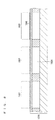
- FIG. 58 is a typical sectional view for describing a conventional method for manufacturing a piezoelectric/electrostrictive film type element 9 constituting an essential part of an ink jetting piezoelectric/electrostrictive actuator to be applied to a head of an ink jet printer.
- a conductive material paste is applied by screen printing onto the front surface of a substrate 902 formed with a cavity 926 which is to serve as an ink pressure room and the obtained coating film is fired into a lower electrode film 912.
- a piezoelectric/electrostrictive material paste is applied by screen printing to the lower electrode film 912 and the obtained coating film is fired into a piezoelectric/electrostrictive film 914.
- an electroconductive material paste is applied by screen printing on the piezoelectric/electrostrictive film 914 and the obtained coating film is fired into an upper electrode film 916.
- Patent Document 1 discloses a method for manufacturing an ink jetting piezoelectric/electrostrictive actuator to be used for the head of an ink jet printer.
- Patent Document 1 Japanese Patent No. 3999044
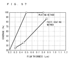
- the conventional manufacturing method has the problem that pores are increased in the lower electrode film by the firing performed after the lower electrode film is formed, leading to a reduction in the coverage of the lower electrode film. This problem is particularly significant when the film thickness of the lower electrode film is reduced to increase the amount of displacement of flexure.
- the conventional manufacturing method has the problem that the plane position of the lower electrode film is deviated from the plane position of the cavity by a dimensional variation and deformation of the substrate and screen plate, causing a variation in the amount of ink to be jetted from the piezoelectric/electrostrictive actuator.
- the present invention has been achieved in view of the above problems, and an object of the present invention is to provide a method for manufacturing a piezoelectric/electrostrictive film type element, which can increase the coverage of the lowermost electrode film and prevent deviation of the plane position of the cavity from the plane position of the lowermost electrode film.
- a first invention relates to a method for manufacturing a piezoelectric/electrostrictive film type element provided with: a substrate formed with a cavity; and an vibrating laminate obtained by laminating electrode films and a piezoelectric/electrostrictive film which are aligned with a plane position of the cavity, on a first principal plane of the substrate, the method including the steps of: (a) producing the substrate; (b) forming a first photoresist film on the first principal plane of the substrate; (c) carring out irradiation with light from a second principal plane side of the substrate to discribe in the first photoresist film a latent image obtained by transferring the plane shape of the cavity; (d) removing, by developing, the first photoresist film formed in a region where the cavity is formed, to form a first photoresist film pattern; (e) forming a resinate film containing a resinate of a catalyst metal on the first principal plane of the substrate such that the resinate film is overlapped on the first
- a second invention relates to the method for manufacturing a piezoelectric/electrostrictive film type element in the first invention, wherein the step (a) is carried out to produce the substrate on which the first principal plane is spaced away from the cavity by a plate having a plate thickness of 30 ⁇ m or less.
- a third invention relates to the method for manufacturing a piezoelectric/electrostrictive film type element in the first or second invention, the method further including the step of: (j) filling a light-shielding agent into the cavity before the step (c), wherein the step (c) is carried out to selectively expose the first photoresist film formed in a region where the cavity is not formed, and the step (d) is carried out to remove an unexposed part of the first photoresist film.
- a fourth invention relates to the method for manufacturing a piezoelectric/electrostrictive film type element in the third invention, wherein the step (j) is carried out to fill the light-shielding agent containing a pigment.
- a fifth invention relates to the method for manufacturing a piezoelectric/electrostrictive film type element in the first or second invention, wherein the step (c) is carried out to selectively expose the first photoresist film formed in the region where the cavity is formed, and the step (d) is carried out to remove the exposed part of the first photoresist film.
- a sixth invention relates to the method for manufacturing a piezoelectric/electrostrictive film type element in the fifth invention, the method further including the step of: (k) forming a light-shielding film in the region where the cavity is not formed on the second principal plane of the substrate before the step (c).
- a seventh invention relates to the method for manufacturing a piezoelectric/electrostrictive film type element in the sixth invention, wherein the step (k) is carried out to form the light-shielding film containing a pigment.
- An eighth invention relates to the method for manufacturing a piezoelectric/electrostrictive film type element in any one of the first to seventh inventions, wherein the step (i) further includes the steps of: (i-1) forming a second photoresist film on the first principal plane of the substrate such that the second photoresist film is overlapped on an optional piezoelectric/electrostrictive film constituting the vibrating laminate; (i-2) carring out irradiation with light from the second principal plane side of the substrate to selectively expose the second photoresist film formed in a region where the optional piezoelectric/electrostrictive film is not formed; (i-3) removing an unexposed part of the second photoresist film to form a second photoresist film pattern; (i-4) forming an electrode film constituting the vibrating laminate in a region where the second photoresist film pattern is not formed; and (i-5) removing the second photoresist film pattern.
- a ninth invention relates to the method for manufacturing a piezoelectric/electrostrictive film type element in any one of the first to eighth inventions, wherein the step (i) further includes the steps of: (i-6) forming a third photoresist film on the first principal plane of the substrate such that the third photoresist film is overlapped on an optional electrode film constituting the vibrating laminate; (i-7) carring out irradiation with light from the second principal plane side of the substrate to selectively expose the third photoresist film formed in a region where the optional electrode film is not formed; (i-8) removing an unexposed part of the third photoresist film to form a third photoresist film pattern; (i-9) forming a piezoelectric/electrostrictive film constituting the vibrating laminate in a region where the third photoresist film pattern is not formed; and (i-10) removing the third photoresist film pattern.
- a tenth invention relates to the method for manufacturing a piezoelectric/electrostrictive film type element in any one of the first to ninth inventions, wherein the step (i) further includes the step of: (i-11) making a piezoelectric/electrostrictive material flow toward an optional electrode film constituting the vibrating laminate by electrophoresis to form a piezoelectric/electrostrictive film constituting the vibrating laminate.
- An eleventh invention relates to the method for manufacturing a piezoelectric/electrostrictive film type element in any one of the first to tenth inventions, the method further including the step of: (l) coating the first photoresist film pattern with a water-repellent film having higher water repellency than the first photoresist film pattern after the step (d) and before the step (e).
- a twelfth invention relates to the method for manufacturing a piezoelectric/electrostrictive film type element in the eleventh invention, wherein the step (l) includes the steps of: (l-1) forming a masking film on the first principal plane of the substrate such that the masking film is overlapped on the first photoresist film pattern; (1-2) removing the masking film until the first photoresist film pattern is exposed to form a masking film pattern; (1-3) forming a water-repellent film on the first principal plane of the substrate such that the water-repellent film is overlapped on the first photoresist film pattern and the masking film pattern; and (1-4) removing the masking film pattern and the water-repellent film formed on the masking film pattern.
- a thirteenth invention relates to a method for manufacturing a piezoelectric/electrostrictive film type element provided with: a substrate formed with a cavity; and an vibrating laminate obtained by laminating electrode films and a piezoelectric/electrostrictive film which are aligned with a plane position of the cavity, on a first principal plane of the substrate, the method including the steps of: (a) producing the substrate; (b) forming a first photoresist film on the first principal plane of the substrate; (c) carring out irradiation with light from a second principal plane side of the substrate to discribe in the first photoresist film a latent image obtained by transferring the plane shape of the cavity; (d) removing, by developing, the first photoresist film formed in a region where the cavity is formed, to form a first photoresist film pattern; (e) forming a catalyst layer in which catalyst metal cores exist in a dispersed state on the first principal plane of the substrate such that the catalyst layer is overlapped on
- a fourteenth invention relates to the method for manufacturing a piezoelectric/electrostrictive film type element in the thirteenth invention, the method further including the step of: (i) coating the first photoresist film pattern with a water-repellent film having higher water repellency than the first photoresist film pattern after the step (d) and before the step (e).
- a fifteenth invention relates to the method for manufacturing a piezoelectric/electrostrictive film type element in the fourteenth invention, wherein the step (i) includes the steps of: (i-1) forming a masking film on the first principal plane of the substrate such that the masking film is overlapped on the first photoresist film pattern; (i-2) removing the masking film until the first photoresist film pattern is exposed to form a masking film pattern; (i-3) forming a water-repellent film on the first principal plane of the substrate such that the water-repellent film is overlapped on the first photoresist film pattern and the masking film pattern; and (i-4) removing the masking film pattern and the water-repellent film formed on the masking film pattern.
- a sixteenth invention relates to the method for manufacturing a piezoelectric/electrostrictive film type element in the thirteenth invention, the method further including the step of: (j) surface-roughing the first principal plane of the substrate after the step (a) and before the step (b).
- a seventeenth invention relates to the method for manufacturing a piezoelectric/electrostrictive film type element in the thirteenth invention, the method further including the step of: (k) forming an adhesive layer which improves adhesion of the plating film, on the first principal plane of the substrate, after the step (a) and before the step (b).
- An eighteenth invention relates to the method for manufacturing a piezoelectric/electrostrictive film type element in any one of the thirteenth to seventeenth inventions, wherein the step (e) is carried out to bring a catalyst metal solution prepared by dissolving a catalyst metal in a solvent, into contact with the first principal plane of the substrate.
- a nineteenth invention relates to the method for manufacturing a piezoelectric/electrostrictive film type element in any one of the thirteenth to seventeenth inventions, wherein the step (e) is carried out to bring a catalyst metal dispersion solution prepared by dispersing catalyst metal microparticles in a dispersing medium, into contact with the first principal plane of the substrate.
- a twentieth invention relates to the method for manufacturing a piezoelectric/electrostrictive film type element in any one of the thirteenth to seventeenth inventions, wherein the step (e) is carried out to deposit a catalyst metal on the first principal plane of the substrate by vapor deposition.
- a twenty-first invention relates to a method for manufacturing a piezoelectric/electrostrictive film type element provided with: a substrate formed with a cavity; and an vibrating laminate obtained by laminating electrode films and a piezoelectric/electrostrictive film which are aligned with a plane position of the cavity, on a first principal plane of the substrate, the method including the steps of: (a) producing the substrate; (b) forming a first photoresist film on the first principal plane of the substrate; (c) carring out irradiation with light from a second principal plane side of the substrate to discribe in the first photoresist film a latent image obtained by transferring the plane shape of the cavity; (d) removing, by developing, the first photoresist film formed in a region where the cavity is not formed, to form a first resist film pattern; (e) forming a water-repellent film on the first principal plane of the substrate such that the water-repellent film is overlapped on the first photoresist film
- a twenty-second invention relates to a method for manufacturing a piezoelectric/electrostrictive film type element provided with: a substrate formed with a cavity; and an vibrating laminate obtained by laminating electrode films and a piezoelectric/electrostrictive film which are aligned with a plane position of the cavity, on a first principal plane of the substrate, the method including the steps of: (a) producing the substrate; (b) forming a first photoresist film on the first principal plane of the substrate; (c) carring out irradiation with light from a second principal plane side of the substrate to discribe in the first photoresist film a latent image obtained by transferring the plane shape of the cavity; (d) removing, by developing, the first photoresist film formed in a region where the cavity is not formed, to form a first photoresist film pattern; (e) forming a water-repellent film on the first principal plane of the substrate such that the water-repellent film is overlapped on the first photore
- the packing density of the lowermost electrode film is improved, and heat resistance is also improved, and therefore, the coverage of the lowermost electrode film is increased. Further, since the lowermost electrode film is formed in the region where the cavity is formed, deviation of the plane position of the cavity from the plane position of the lowermost electrode film is limited.
- the temperature of the region where the cavity is formed is uniformed, and therefore, the lowermost electrode film is uniformly formed in the region where the cavity is formed.
- the resolution of patterning is improved.
- the resolution of patterning is improved because the difference between the light transmittance in the region where the cavity is formed and the light transmittance in the region where the cavity is not formed is increased.
- the resolution of patterning is further improved.
- the electrode film is formed in the region where the piezoelectric/electrostrictive film is formed, and therefore, deviation of the plane position of the piezoelectric/electrostrictive film from the plane position of the electrode film is limited.
- the piezoelectric/electrostrictive film is formed in the region where the electrode film is formed, and therefore, deviation of the plane position of the electrode film from the plane position of the piezoelectric/electrostrictive film is limited.
- the piezoelectric/electrostrictive film is formed in the region including the region where the electrode film is formed, deviation of the plane position of the electrode film from the plane position of the piezoelectric/electrostrictive film is limited.
- the end tail projection of the lowermost electrode film is limited.
- heat resistance of the lowermost electrode film is improved, and therefore, the coverage of the lowermost electrode film is increased. Further, since the lowermost electrode film is formed in the region where the cavity is formed, deviation of the plane position of the cavity from the plane position of the lowermost electrode film is limited.
- the fourteenth invention since the surface on which the lowermost electrode film is formed is roughened, adhesion of the lowermost electrode film is improved.
- the adhesive layer which improves adhesion of the lowermost electrode film is formed on the surface on which the lowermost electrode film is formed, and therefore, adhesion of the lowermost electrode film is improved.
- heat resistance of the lowermost electrode film is improved, and therefore, the coverage of the lowermost electrode film is increased. Further, since the lowermost electrode film is formed in the region where the cavity is formed, deviation of the plane position of the cavity from the plane position of the lowermost film is limited. Moreover, since the lowermost electrode film is repelled by the water-repellent film, the end tail projection of the lowermost electrode film is limited.
- heat resistance of the lowermost electrode film is improved, and therefore, the coverage of the lowermost electrode film is increased. Further, since the lowermost electrode film is formed in the region where the cavity is formed, deviation of the plane position of the cavity from the plane position of the lowermost film is limited. Moreover, since the lowermost electrode film is repelled by the water-repellent film, the end tail projection of the lowermost electrode film is limited.
- a piezoelectric/electrostrictive film type element provided with a substrate formed with a cavity and an vibrating laminate obtained by laminating a lower electrode film, a piezoelectric/electrostrictive film, an upper electrode film which are aligned with the plane position of the cavity, on the front surface of the substrate, the lower electrode film is formed by using, as a mask, the substrate in which the cavity is filled with a light-shielding agent according to photolithography.
- a powder of piezoelectric/electrostrictive material is made to flow toward the lower electrode film by electrophoresis to form a piezoelectric/electrostrictive film and then, an upper electrode film is formed using the piezoelectric/electrostrictive material as a mask according to the photolithography.
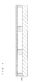
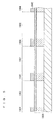
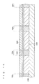
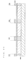
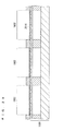
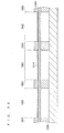
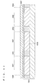
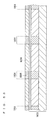
- FIGS. 1 to 3 are typical views each showing a schematic structure of a piezoelectric/electrostrictive film type element 1002 manufactured by the method for manufacturing a piezoelectric/electrostrictive film type element according the first embodiment of the present invention.
- FIG. 1 is a perspective view of the piezoelectric/electrostrictive film type element 1002
- FIG. 2 is a sectional view of the piezoelectric/electrostrictive film type element 1002 taken along line II-II of FIG. 1
- FIG. 3 is a sectional view of the piezoelectric/electrostrictive film type element 1002 taken along line III-III of FIG. 1 .
- the piezoelectric/electrostrictive film type element 1002 constitutes the essential part of the piezoelectric/electrostrictive actuator for ink jetting which is used for the head of an ink jet printer.
- the following method for manufacturing a piezoelectric/electrostrictive film type element may also be utilized for the manufacturing of other types of piezoelectric/electrostrictive film type elements.
- the piezoelectric/electrostrictive film type element 1002 has a structure in which plural vibrating laminates 1004 are regularly arranged on a front surface of a substrate 1006.
- the following method for manufacturing a piezoelectric/electrostrictive film type element may also be utilized for the manufacturing of a piezoelectric/electrostrictive film type element provided with only one vibrating laminate 1004.
- the piezoelectric/electrostrictive film type element 1002 has a sectional structure in which the vibrating laminate 1004 obtained by laminating a lower electrode film 1014, a piezoelectric/electrostrictive film 1016 and an upper electrode film 1018 in this order from bottom to top is formed on the front surface of the substrate 1006 in which a base plate 1008, a base plate 1010 and an vibrating plate 1012 are laminated in this order from bottom to top.
- the substrate 1006 is a fired body of an insulating ceramics.
- the insulating ceramics preferably contains at least one type selected from the group consisting of zirconium oxide, aluminum oxide, magnesium oxide, mullite, aluminum nitride, and silicon nitride in view of heat resistance, chemical stability, and insulating ability, though no particular limitation is imposed on the type of insulating ceramics.
- stabilized zirconium oxide is preferable in view of mechanical strength and toughness.
- the "stabilized zirconium oxide” indicates zirconium oxide limited in the phase transfer of a crystal by adding a stabilizer, and includes, besides stabilized zirconium oxide, partially stabilized zirconium oxide.
- the base plate 1008 has a structure in which an ink jetting nozzle 1020 and an ink supply hole 1022 each having a circular plane shape are formed in a plate having an almost even thickness.
- the ink jetting nozzle 1020 is formed in the vicinity of one end of a region (hereinafter referred to as a "cavity region") 1902 where a cavity 1024 (which will be described later) is formed and the ink supply hole 1022 is formed in the vicinity of the other end of the cavity region 1902.
- the base plate 1010 has a structure in which a cavity 1024 having an elongated rectangular plane shape is formed in a plate having an almost even thickness.
- the width W1 of the short side of the cavity 1024 is preferably made larger, and is, specifically, 50 ⁇ m or more to increase the amount of displacement of flexure which will be described later to thereby increase the volume to be excluded.
- the width W1 of the cavity 1024 is preferably 100 ⁇ m or less.
- the length L of the long side of the cavity 1024 is preferably shorter, and is, specifically, 3 mm or less to reduce flow resistance.
- the width W2 of a frame 1026 extended between the neighboring cavities 1024 is preferably smaller, and is, specifically, 100 ⁇ m or less to increases the amount of displacement of flexure to thereby increase the volume to be excluded.
- the plane shape of the cavity 1024 is not limited to an elongated rectangular form.
- the plane shape of the cavity 1024 may be a polygonal form such as a triangle or square form, or a two-dimensional form, such as a circular or elliptical form in which a part of the profile is curved. Further, it is unessential to arrange the cavities 1024 in one direction and for example, the cavities 1024 may be arranged lattice-wise in two orthogonal directions.
- the vibrating plate 1012 is a plate having an almost even thickness.
- the plate thickness of the vibrating plate 1012 is preferably 1 ⁇ m or more and 30 ⁇ m or less and more preferably 1 ⁇ m or more and 15 ⁇ m or less. It is because if the plate thickness thereof is less than this range, the vibrating plate 1012 is easily damaged whereas if the plate thickness thereof exceeds this range, the rigidity of the vibrating plate 1012 is high, and therefore the amount of displacement of flexure tends to decrease. It is unessential that the vibrating plate 1012 is flat, and even if the vibrating plate 1012 has slight irregularities and warpage, the following method for manufacturing a piezoelectric/electrostrictive film type element is adopted.
- the laminate structure of the base plate 1008, base plate 1010 and vibrating plate 1012 allows the cavity 1024 to form a hollow space which is isolated from the front surface side by the vibrating plate 1012 and from the back surface side by the base plate 1010 inside of the substrate 1006 and to function as an ink room which stores ink.
- the ink jetting nozzle 1020 is communicated with the cavity 1024 and functions as a path for ink flowed from the cavity 1024.
- the ink supply hole 1022 is also communicated with the cavity 1024 and functions as a path for ink flowed into the cavity 1024.
- the sum of the plate thicknesses of the base plate 1008, base plate 1010 and vibrating plate 1012 is so determined that the exposure light transmitted therefrom is sufficient as will be described later. What order to select as the sum of plate thicknesses for sufficient transmission of exposure light, of course, varies depending on the type of insulating ceramics and the density of the fired body.
- the lower electrode film 1014 is a plating precipitate of a conductive material.
- the upper electrode film 1018 is a fired body of a conductive material.
- the upper electrode film 1018 may be a plating precipitate of a conductive material.
- a metal such as platinum, palladium, rhodium, gold or silver or an alloy containing each of these metals as its major component is preferable in view of electric resistance and heat resistance.
- platinum or an alloy containing platinum as its major component which is particularly superior in heat resistance is preferable.
- the film thickness of the lower electrode film 1014 is preferably 0.1 ⁇ m or more and 5.0 ⁇ m or less
- the film thickness of the upper electrode film 1018 is preferably 0.1 ⁇ m or more and 3.0 ⁇ m or less. It is because when the thicknesses exceed these ranges, the rigidity of each of the lower electrode film 1014 and the upper electrode film 1018 is increased and the amount of displacement of flexure tends to decrease, whereas when these thicknesses are less than these ranges, the electric resistance of each of the lower electrode film 1014 and the upper electrode film 1018 tends to increase and the lower electrode film 1014 and the upper electrode film 1018 tend to be disconnected.
- the lower electrode film 1014 and the upper electrode film 1018 are preferably formed in such a manner as to cover the region which substantially contributes to the displacement of flexure of the piezoelectric/electrostrictive film 1016.
- these electrode films are preferably formed in such a manner as to cover a region 80% or more of the upper surface and lower surface of the piezoelectric/electrostrictive film 1016 including the center part of the piezoelectric/electrostrictive film 1016.
- the piezoelectric/electrostrictive film 1016 is a fired body of piezoelectric/electrostrictive ceramics.
- the material of the ceramics is preferably a lead (Pb) type perovskite oxide and more preferably lead zirconate titanate (PZT; Pb(Zr x Ti 1-x )O 3 ) or modified products obtained by introducing a simple oxide or complex perovskite oxide into lead zirconate titanate in view of electric field induced strain.
- ceramics obtained by introducing nickel oxide (NiO) into a solid solution of lead zirconate titanate and a lead magnesium niobate (Pb(Mg 1/3 Nb 2/3 )O 3 ) and a solid solution of lead zirconate titanate and a lead nickel niobate (Pb(Ni 1/3 Nb 2/3 )O 3 ) are preferable.
- the film thickness of the piezoelectric/electrostrictive film 1016 is preferably 1 ⁇ m or more and 20 ⁇ m or less. This is because when the film thickness is less than this range, the piezoelectric/electrostrictive film 1016 tend to be insufficiently densified, whereas when the film thickness exceeds this range, it is necessary to increase the thickness of the vibrating plate 1012 because the shrinkage stress of the piezoelectric/electrostrictive film 1016 in the sintering is increased.
- the vibrating laminate 1004 is provided with a lower wiring electrode 1028 which is to serve as a power feed path to the lower electrode film 1014 and an upper wiring electrode 1030 which is to serve as a power feed path to the upper electrode film 1018.
- One end of the lower wiring electrode 1028 is disposed between the lower electrode film 1014 and the piezoelectric/electrostrictive film 1016 and is electrically connected to one end of the lower electrode film 1014 and the other end of the lower wiring electrode 1028 is disposed in a non-cavity region 1904 out of the cavity region 1902.
- One end of the upper wiring electrode 1030 is disposed above the upper electrode film 1018 and is electrically connected to one end of the upper electrode film 1018 and the other end of the upper wiring electrode film 1018 is disposed in the non-cavity region 1904.
- the vibrating laminate 1004 is integrated with the vibrating plate 1012 above the cavity 1024.
- Such a structure ensures that when drive signals are fed between the lower electrode film 1014 and the upper electrode film 1018 through the lower wiring electrode 1028 and upper wiring electrode 1030 to apply an electric field to the piezoelectric/electrostrictive film 1016, the piezoelectric/electrostrictive film 1016 is expanded and shrunk in a direction parallel to the front surface of the substrate 1006, causing the flexural displacement of the integrated piezoelectric/electrostrictive film 1016 and vibrating plate 1012. Ink inside of the cavity 1024 is jetted toward the outside through the ink jetting nozzle 1020 by this flexural displacement.
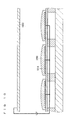
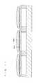
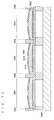
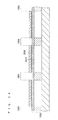
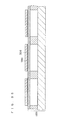
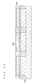
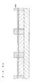
- FIGS. 4 to 15 are typical views for describing the method for manufacturing the piezoelectric/electrostrictive film type element according to the first embodiment.
- FIGS. 4 to 15 are sectional views of the half-finished product of the piezoelectric/electrostrictive film type element 1002.
- the substrate 1006 is produced as shown in FIG. 4 .
- the substrate 1006 is produced, for example, by crimping a green sheet obtained by molding insulating ceramics into a sheet, followed by firing.
- a resist film pattern 1042 which does not cover the cavity region 1902 but covers the non-cavity region 1904 is formed on the front surface of the substrate 1006.
- the resist film pattern 1042 is formed by patterning the resist film covering the front surface of the substrate 1006 by photolithography using the substrate 1006 as a mask.
- a resinate film 1044 is formed on the front surface of the substrate 1006 such that it is overlapped on the resist film pattern 1042 as shown in FIG. 6 . There is no problem even if the resinate film 1044 overflows into the non-cavity region 1904 because the resist film pattern 1042 is removed afterward. Also, there is no problem even if the resinate film 1044 is imperfectly formed on the non-cavity region 1904.
- the resinate film 1044 is formed by applying a solution containing a resinate of a catalyst metal (hereinafter referred to as a "catalyst metal resinate solution"), followed by removing a solvent.
- the catalyst metal resinate solution is applied by, for example, spin coating or splaying.
- platinum (Pt), palladium (Pd) or the like is selected as the catalyst metal though an appropriate material is selected according to the type of a conductive material subject to electroless plating.
- the resist film pattern 1042 and the resinate film 1044 formed in the region where the resist film pattern 1042 is formed are removed.
- a resinate film pattern 1045 having the same plane shape as the cavity 1024 is formed on the same plane position as the cavity 1024.
- the resist film pattern 1042 is peeled by the chemical solution method.
- an organic solvent, hydrazine type or non-hydrazine type strong alkali etching solution or the like is typically selected though it is selected corresponding to the photosensitive material of the resist film pattern 1042.
- the resist film pattern 1042 may be peeled by the heat treating method, the plasma treating method, or the like. When it is peeled by the heat treating method, the treating temperature is preferably 500°C or more.
- washing gas is jetted toward the half-finished product, a gritting/cleaning agent powder is sprayed on the half-finished product, or the half-finished product is washed with a washing liquid or dipped in a washing liquid to thereby remove the residue.
- the resinate film pattern 1045 is fired as shown in FIG. 8 .
- This ensures formation of the catalyst layer pattern 1046 having the same plane shape as the cavity 1024 on the same plane position as the cavity 1024.
- the "catalyst layer” indicates a layer in which catalyst metal cores exist in a dispersed state in a plane.
- the catalyst metal cores which are the start points of the precipitation of the conductive material are adsorbed.
- the firing is performed at a temperature at which the resinate is decomposed and microparticles which are to serve as the catalyst metal cores are precipitated. Therefore, the firing temperature is selected according to the type of resinate.
- the resinate film pattern 1045 is typically fired at 200 to 1300°C.
- the amount of the catalyst metal contained in the resinate film 1044 is not made to be excessive.
- the content of the catalyst metal in the catalyst metal resinate solution is preferably 0.1% by weight or more and 20% by weight or less.
- the catalyst layer pattern 1046 After the catalyst layer pattern 1046 is formed, a plating film is formed on the catalyst layer pattern 1046 by electroless plating. Thus, the lower electrode film 1014 is formed as shown in FIG. 9 .
- the conductive material is precipitated from a plating solution after the catalyst layer pattern 1046 is reduced.
- the catalyst layer pattern 1046 is reduced by, for example, dipping the half-finished product in a reducing agent solution to bring the reducing agent solution into contact with the catalyst layer pattern 1046.
- a reducing agent solution for example, an aqueous composed solution of sodium hydroxide and sodium borohydride is used.
- the precipitation of the conductive material from the plating solution is performed by bringing the plating solution into contact with the catalyst layer pattern 1046 which is reduced and activated when the half-finished product is dipped in the plating solution.
- the lower electrode film 1014 is uniformly formed in the cavity region 1902 because the temperature of the front surface of the substrate 1006 is uniformed in the cavity region 1902.
- a piezoelectric/electrostrictive material film 1048 which is to serve as the piezoelectric/electrostrictive film 1016 is formed.
- the piezoelectric/electrostrictive material film 1048 is formed by dipping the half-finished product and a counter electrode 1050 spaced away from each other in a slurry in which a piezoelectric/electrostrictive material is dispersed in a dispersing medium and also, voltage is applied to the lower electrode film 1014 and counter electrode 1050 to thereby allow the piezoelectric/electrostrictive material to move toward the lower electrode film 1014 by electrophoresis as shown in FIG. 10 .
- the piezoelectric/electrostrictive material film 1048 having a plane shape slightly larger than the lower electrode film 1014 on the same plane position as the lower electrode film 1014 is formed.
- regions where it is not necessary to form the piezoelectric/electrostrictive film 1048, such as the region where the lower wiring electrode 1028 is formed be masked with an organic protective film or the like and an unnecessary piezoelectric/electrostrictive material be removed together with the organic protective film after the piezoelectric/electrostrictive material film 1048 is formed. Formation of the piezoelectric/electrostrictive material film 1048 on the lower wiring electrode 1028 is prevented by this treatment.
- the piezoelectric/electrostrictive material film 1048 is fired. As shown in FIG. 11 , the piezoelectric/electrostrictive material film 1048 is thereby made into a piezoelectric/electrostrictive film 1016 and the piezoelectric/electrostrictive film 1016 having a plane shape slightly larger than the lower electrode film 1014 on the same plane position as the lower electrode film 1014 is formed. In this case, slight shrinkage caused by firing is allowed.
- the piezoelectric/electrostrictive material film 1048 is preferably fired in the condition that the half-finished product is received in, for example, an alumina or magnesia sheath.
- a resist film pattern 1052 which does not cover a region (hereinafter referred to as "piezoelectric/electrostrictive region") 1906 where the piezoelectric/electrostrictive film 1016 is formed but covers a non-piezoelectric/electrostrictive region 1908 outside of the piezoelectric/electrostrictive material region 1906 is formed on the front surface of the substrate 1006.
- the resist film pattern 1052 is formed by patterning the resist film covering the front surface of the substrate 1006 by photolithography using the piezoelectric/electrostrictive film 1016 as a mask.
- the lower wiring electrode 1028 works as a mask and therefore, the resist film pattern 1052 is not formed on the lower wiring electrode 1028. Therefore, it is preferable to mask a region where it is necessary to form the upper electrode film 1018, such as the region where the lower wiring electrode 1028 is formed, with an organic protective film and then to remove the organic protective film before, after or when the resist film pattern 1052 is removed. This prevents formation of the upper electrode film 1018 on the lower wiring electrode 1028.
- a conductive material film 1054 which is to serve as the upper electrode film 1018, is formed to be overlapped on the piezoelectric/electrostrictive film 1016 in the piezoelectric/electrostrictive region 1906 where the resist film pattern 1052 is not formed on the front surface of the substrate 1006. In this case, there is no problem even if the conductive material film 1054 overflows into the non-piezoelectric/electrostrictive region 1908 because the resist film pattern 1052 is removed afterward.
- the conductive material film 1054 may be formed by applying a conductive paste or a resinate solution (hereinafter referred to as a "conductive resinate solution") prepared by dissolving a resinate of a conductive material in a solvent and then by removing a dispersing medium or solvent, or may be formed by vapor deposition of a conductive material.
- the conductive paste is applied by screen printing or the like and the conductive resinate solution is applied by spin coating, spraying or the like.
- the conductive material is vapor-deposited by, for example, sputter vapor deposition or resistance heating vapor deposition.
- the contact angle of the conductive paste with the resist film pattern 1052 is preferably 50 degrees or more and more preferably 70 degrees or more to limit the end tail projection of the conductive material film 1054.
- the resist film pattern 1052 left in the non-piezoelectric/electrostrictive region 1908 is removed.
- a conductive material film 1054 having the same plane shape as the piezoelectric/electrostrictive film 1016 on the same plane position as the piezoelectric/electrostrictive film 1016 is thereby formed.
- the resist film pattern 1052 is removed in the same manner as the resist film pattern 1042.
- the conductive material film 1054 is fired. As shown in FIG. 15 , the conductive material film 1054 is made into the upper electrode film 1018 and the upper electrode film 1018 having the same plane shape as the piezoelectric/electrostrictive film 1016 is thereby formed on the same plane position as the piezoelectric/electrostrictive film 1016. In this case, slight shrinkage caused by firing is allowed.
- the conductive material film 1054 is fired preferably at a firing temperature of 200°C or more and 300°C or less when the conductive material film 1054 is formed using a conductive paste in which nano-particles of platinum are dispersed in a dispersing medium, by screen printing and at a firing temperature of 1000°C or more and 1350°C or less when the conductive material film 1054 is formed using a conductive paste in which a platinum powder is dispersed in a dispersing medium, by screen printing. Also, when the conductive material film 1054 is formed using a conductive resinate solution prepared by dissolving a platinum resinate in a solvent, by spin coating, the firing temperature is preferably 600°C or more and 800°C or less.
- the upper electrode film 1018 may be formed by electroless plating in the same manner as the lower electrode film 1014.
- An upper wiring electrode 1030 is formed after the conductive material film 1054 is fired.
- the upper wiring electrode 1030 is formed in the same manner as the lower wiring electrode 1028.
- the upper wiring electrode 1030 may be fired at the same time when the upper electrode film 1018 is fired.
- the packing density of the lower electrode film 1014 is improved and also, heat resistance thereof is improved, so that the coverage of the lower electrode film 1014 is increased.
- the piezoelectric/electrostrictive film 1016 is formed in the piezoelectric/electrostrictive region 1906 including the cavity region 1902 where the lower electrode film 1014 is formed, deviation of the plane position of the lower electrode film 1014 from the plane position of the piezoelectric/electrostrictive film 1016 is limited.
- Deviation of the plane position of the cavity 1024 from each plane position of the lower electrode film 1014, piezoelectric/electrostrictive film 1016 and upper electrode film 1018 which constitute the vibrating laminate 1004 is limited, with the result that deviation of the plane position of the cavity 1024 from the plane position of the vibrating laminate 1004 is limited.
- This contributes to restriction on a variation in the amount of ink to be jetted from a piezoelectric/electrostrictive actuator including the piezoelectric/electrostrictive film type element 1002.
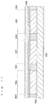
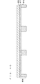
- FIGS. 16 to 21 are typical views for describing the method for forming the resist film pattern 1042 according to the first embodiment.
- FIGS. 16 to 21 are sectional views of a half-finished product of the piezoelectric/electrostrictive film type element 1002.
- a resist film 1056 is formed on the front surface of the substrate 1006.
- the resist film 1056 is formed by applying a resist solution prepared by dissolving a resist solid in a solvent or dispersing the resist solid in a dispersing medium, onto the front surface of the substrate 1006 by a spin coater and by heating the half-finished product by a hot plate, oven or the like to vaporize the solvent from the coating film.
- the resist solution may be applied by other methods such as spraying.
- a negative type photoresist is used which is deteriorated in solubility in a developing solution when it is exposed to light.
- the resist film 1056 is a photosensitive film which is deteriorated in solubility in a developing solution when exposed to light.
- the resist it is preferable to use a thick-film responsive resist suitable to form a thick film and it is more preferable to use a high-aspect responsive resist having the characteristics that even if a pattern having a high aspect ratio is formed, the section of the pattern scarcely has a tapered form.
- an appropriate material for the resist is selected from photosensitive materials, such as a polyimide and fluororesin resistant to strong alkalis.
- the cavity 1024 is filled with a light-shielding agent 1058 to impart, to the substrate 1006, a function as a mask which shields the cavity region 1902 but does not shield the non-cavity region 1904 as shown in FIG. 17 .
- the filling of the light-shielding agent 1058 into the cavity 1024 is accomplished only by carrying out before the irradiation with light from the back surface side which will be described later. Therefore, the resist film 1056 may be formed on the front surface of the substrate 1006 after the light-shielding agent 1058 is filled into the cavity 1024.
- the filling of the light-shielding agent 1058 into the cavity 1024 is performed by injecting a light-shielding solution prepared by dissolving a solid of the light-shielding agent 1058 in a solvent or by dispersing the solid thereof in a dispersing medium, into the ink jetting nozzle 1020 or the ink supply hole 1022 by an injector, and by heating the half-finished product by, for example, a hot plate or an oven to dry the light-shielding solution.
- a porous material such as a sintered metal impregnated with the light-shielding solution may be brought into contact with the back surface of the substrate 1006 to allow the light-shielding solution to flow into the cavity 1024 from the porous material by the capillary phenomenon. Additionally, after the light-shielding solution is injected, vacuum defoaming may be carried out.
- the light-shielding agent 1058 preferably contains a dye or a pigment which absorbs light for exposure, and more preferably contains a pigment. This is because the resolution of patterning is improved when the light-shielding agent 1058 contains a pigment.
- the optical concentration of the light-shielding agent 1058 is preferably 2 to 3 on OD value basis.
- a light-shielding agent 1058 differing in refractive index from the substrate 1006 may be used to totally reflect light for exposure in the cavity region 1902.
- the unexposed part 1060 of the resist film 1056 which is formed in the cavity region 1902 is removed by developing as shown in FIG. 19 .
- the latent image is developed by dipping the half-finished product in a developing solution with fluctuation to remove the unexposed part 1060, followed by washing the half-finished product with pure water or the like.
- a developing solution a solution which selectively dissolves the unexposed part 1060 but does not dissolve the exposed part 1062 is selected.
- Irradiation with light from the front surface side of the substrate 1006 is carried out to further expose the exposed part 1062 left in the non-cavity region 1904 to burn the exposed part 1062 to a solid.
- the resist film pattern 1042 is thereby completed as shown in FIG. 20 .
- the light-shielding agent 1058 is removed from the cavity 1024 as shown in FIG. 21 .
- the removal of the light-shielding agent 1058 from the cavity 1024 is accomplished only by carrying out after the aforementioned irradiation with light from the back surface side. Therefore, the unexposed part 1060 may be removed after the light-shielding agent 1058 is removed from the cavity 1024.
- the removal of the light-shielding agent 1058 from the cavity 1024 is carried out by dipping the half-finished product in a solvent.
- FIGS. 22 to 25 are typical views for describing a method for forming the resist film pattern 1052 according to the first embodiment.
- FIGS. 22 to 25 are sectional views of a half-finished product of the piezoelectric/electrostrictive film type element 1002.
- a resist film 1064 is formed on the front surface of the substrate 1006 in such a manner that it is overlapped on the piezoelectric/electrostrictive film 1016 as shown in FIG. 22 .
- the resist film 1064 is formed in the same manner as the resist film 1056 and in formation of the resist film 1064, the same resist as that used for forming the resist film 1056 is used.
- the unexposed part 1066 of the resist film 1064 formed in the piezoelectric/electrostrictive region 1906 is removed by developing as shown in FIG. 24 .
- the latent image is developed in the same manner as the latent image formed on the resist film 1056 and in the developing of the latent image, the same developing solution as that used in the case of developing the latent image discribed on the resist film 1056 is used.
- the resist film pattern 1052 is thus completed as shown in FIG. 25 .
- a second embodiment relates to a method for forming a lower electrode film 2014 which is adopted in place of the method for forming the lower electrode film 1014 according to the first embodiment.
- a half-finished product is dipped in a catalyst metal solution to form a catalyst layer 2046.
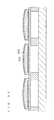
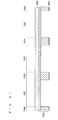
- FIGS. 26 to 31 are views for describing the method for forming the lower electrode film 2014 according to the second embodiment.
- FIGS. 26 to 31 are sectional views of a half-finished product of the piezoelectric/electrostrictive film type element 1002.
- the front surface of the substrate 1006 is roughened as pretreatment in the method for forming the lower electrode film 2014 according to the second embodiment. Since the surface on which the lower electrode film 2014 is formed is roughened, adhesion of the lower electrode film 2014 is improved.
- the front surface of the substrate 1006 may be roughened either by chemical action such as wet etching or dry etching using a fluorine compound or by physical action such as dry blasting, wet blasting or vacuum blasting.
- pretreatment in which an adhesive layer 2102 which improves adhesion of the lower electrode film 2014 is formed on the front surface of the substrate 1006 may be carried out instead of the pretreatment in which the front surface of the substrate 1006 is roughened.
- the adhesive layer 2102 is typically formed on the front surface of the substrate 1006 by forming a thin film of a metal such as titanium or chromium by vapor deposition such as sputter vapor deposition or resistance heating vapor deposition, though it is a layer more highly adhesive to the lower electrode film 2014 than the front surface of the substrate 1006.
- a resist film pattern 2042 which does not cover the cavity region 1902 but covers the non-cavity region 1904 is formed on the front surface of the substrate 1006 as shown in FIG. 27 .
- the resist film pattern 2042 is formed in the same manner as the resist film pattern 1042 described in the first embodiment.
- a catalyst layer 2046 is formed on the front surface of the substrate 1006 in such a manner that it is overlapped on the resist film pattern 2042 as shown in FIG. 28 .
- the catalyst layer 2046 overflows into the non-cavity region 1904 because the resist film pattern 2042 is removed afterward.
- formation of the catalyst layer 2046 in the non-cavity region 1904 is imperfect, there is no problem.
- the catalyst layer 2046 is formed, for example, by dipping the half-finished product in a catalyst metal solution prepared by dissolving a catalyst metal in a solvent to bring the catalyst metal solution into contact with the front surface of the substrate 1006 in which the resist film pattern 2042 is left in the non-cavity region 1904 and by drying to remove the solvent stuck onto the front surface of the substrate 1006.
- a catalyst metal dispersion solution obtained by dispersing catalyst metal micro-particles in a dispersing medium may be used instead of the catalyst metal solution and may be brought into contact with the front surface of the substrate 1006, followed by drying to remove the dispersing medium stuck onto the front surface of the substrate 1006.
- the catalyst metal is platinum
- an aqueous chloro-platinic acid solution is used as the catalyst metal solution and for example, a platinum nano-colloid dispersion solution is used as the catalyst metal dispersion solution.
- a metal microparticle dispersion paste may be used in place of the platinum nano-colloid dispersion solution.
- the metal microparticle dispersion paste include metal nano-pastes which can be sintered at normal temperature.
- the catalyst layer 2046 is formed also by vapor-depositing the catalyst metal on the front surface of the substrate 1006 in which the resist film pattern 2042 is left in the non-cavity region 1904 by, for example, sputter vapor deposition or resistance heating vapor deposition.
- the film thickness of the catalyst layer 2046 is preferably 0.01 to 0.1 ⁇ m.
- a plating film is formed on the catalyst layer 2046 by electroless plating. As shown in FIG. 29 , the lower electrode film 2014 is thereby formed in the cavity region 1902.
- the resist film pattern 2042 left in the non-cavity region 1904 is peeled and removed as shown in FIG. 30 .
- the resist film pattern 2042 is peeled in the same manner as the resist film pattern 1042 described in the first embodiment.
- the pack density of the lower electrode film 2014 is improved and also, heat resistance is improved, and therefore, the coverage of the lower electrode film 2014 is increased.
- the lower electrode film 2014 is formed in the cavity region 1902, deviation of the plane position of the cavity 1024 from the plane position of lower electrode film 2014 is limited. This ensures that the lower electrode film 2014 to be adopted instead of the lower electrode film 1014 adopted in the first embodiment is provided.
- a third embodiment relates to a method for forming a piezoelectric/electrostrictive film 3016 which is adopted instead of the method for forming the piezoelectric/electrostrictive film 1016 described in the first embodiment.
- the piezoelectric/electrostrictive film 3016 is formed using the lower electrode film 1014 as a mask by photolithography.
- FIGS. 32 to 35 are typical views for describing the method for forming the piezoelectric/electrostrictive film 3016 according to the third embodiment.
- FIGS. 32 to 35 are sectional views of a half-finished product of the piezoelectric/electrostrictive film type element 1002.
- a resist film pattern 3302 which does not cover the cavity region 1902 but covers the non-cavity region 1904 is formed on the front surface of the substrate 1006 as shown in FIG. 32 .
- the resist film pattern 3302 is formed by patterning the resist film which covers the front surface of the substrate 1006 by using the lower electrode film 1014 as a mask.
- a piezoelectric/electrostrictive material film 3048 which is to serve as a piezoelectric/electrostrictive film 3016, is formed to be overlapped on the lower electrode film 1014 in the cavity region 1902 where the resist film pattern 3302 is not formed on the front surface of the substrate 1006, as shown in FIG. 33 .
- the piezoelectric/electrostrictive material film 3048 overflows into the non-cavity region 1904, there is no problem because the resist film pattern 3302 is removed afterward.
- the piezoelectric/electrostrictive material film 3048 is formed by applying a paste (hereinafter referred to as a "piezoelectric/electrostrictive paste") obtained by dispersing a piezoelectric/electrostrictive material in a dispersing medium, followed by removing the dispersing medium.
- the piezoelectric/electrostrictive paste is applied by screen printing or the like.
- the contact angle of the piezoelectric/electrostrictive paste with the resist film pattern 3302 is preferably 50 degrees or more and more preferably 70 degrees or more.
- the resist film pattern 3302 left in the non-cavity region 1904 where the lower electrode film 1014 is not formed is removed as shown in FIG. 34 . This results in formation of the piezoelectric/electrostrictive material film 3048 having the same plane shape as the lower electrode film 1014 on the same plane position as the lower electrode film 1014.
- the resist film pattern 3302 is peeled in the same manner as the resist film pattern 1042 used in the first embodiment.
- the piezoelectric/electrostrictive material film 3048 is fired. As shown in FIG. 35 , the piezoelectric/electrostrictive material film 3048 thereby becomes the piezoelectric/electrostrictive film 3016 and the piezoelectric/electrostrictive film 3016 having the same plane shape as the lower electrode film 1014 is formed on the same plane position as the lower electrode film 1014. In this case, slight shrinkage caused by firing is allowed. The piezoelectric/electrostrictive material film 3048 is fired in the same manner as the piezoelectric/electrostrictive material film 1048 described in the first embodiment.
- the piezoelectric/electrostrictive film 3016 is formed in the cavity region 1902 where the lower electrode film 1014 is formed and therefore, deviation of the plane position of the lower electrode film 1014 from the plane position of the piezoelectric/electrostrictive film 3016 is limited. This allows the production of the piezoelectric/electrostrictive film 3016 to be adopted in place of the piezoelectric/electrostrictive film 1016 described in the first embodiment.
- FIGS. 36 to 39 are typical views for describing a method for forming a resist film pattern 3302 according to the third embodiment.
- FIGS. 36 to 39 are sectional views of a half-finished product of a piezoelectric/electrostrictive film type element.
- a resist film 3304 is formed on the front surface of the substrate 1006 such that it is overlapped on the lower electrode film 1014 as shown in FIG. 36 .
- the resist film 3304 is formed in the same manner as the resist film 1056 of the first embodiment. In formation of the resist film 3304, the same resist that is used to form the resist film 1056 of the first embodiment is used.
- Irradiation with light from the back surface side of the substrate 1006 is carried out to selectively expose the resist film 3304 formed in the non-cavity region 1904 where the lower electrode film 1014 is not formed to form an unexposed part 3306 and an exposed part 3308 as shown in FIG. 37 .
- a latent image obtained by reverse transfer of the plane shape of the lower electrode film 1014 is thus discribed on the resist film 3304.
- the unexposed part 3306 of the resist film 3304 formed in the cavity region 1902 is removed by developing as shown in FIG. 38 .
- the latent image is developed in the same manner as the latent image discribed on the resist film 1056 and, specifically, the latent image is developed using the same developing solution as that used to develop the latent image discribed on the resist film 1056.
- Irradiation with light from the front surface side of the substrate 1006 is carried out to further expose the exposed part 3308 left in the non-cavity region 1904, thereby burning the exposed part 3308 to a solid.
- the resist film pattern 3302 is thus completed as shown in FIG. 39 .
- a fourth embodiment relates to a method for forming a resist film pattern 4042 to be adopted instead of the method for forming the resist film pattern 1042 according to the first embodiment.
- FIGS. 40 to 45 are typical views for describing a method for forming a resist film pattern 4042 according to the fourth embodiment.
- FIGS. 40 to 45 are sectional views of a half-finished product of the piezoelectric/electrostrictive film type element 1002.
- a positive type photoresist is used.
- a resist film 4056 is formed on a front surface of a substrate 4006 prepared by laminating a base plate 4010 and an vibrating plate 4012 in this order from bottom to top as shown in FIG. 40 .
- the plate thickness of the vibrating plate 4012 is also preferably 30 ⁇ m or less.
- the resist film 4056 is formed in the same manner as the resist film 1056.
- As the resist a positive type photoresist is used which is increased in solubility in a developing solution when it is exposed to light. Therefore, the resist film 4056 is a photosensitive film which is increased in solubility in a developing solution when it is exposed to light.
- the resist it is preferable to use a thick-film responsive resist suitable to form a thick film and it is more preferable to use a high-aspect responsive resist having the characteristics that even if a pattern having a high aspect ratio is formed, the section of the pattern scarcely has a tapered form.
- an appropriate material for the resist is selected from composite materials of photosensitive materials and photo-insensitive materials, such as a polyimide and fluororesin resistant to strong alkalis.
- a light-shielding film 4402 is formed in the non-cavity region 1904 on the back surface of the substrate 4006 to impart, to the substrate 4006, a function as a mask which shields the non-cavity region 1904 but does not shield the cavity region 1902 as shown in FIG. 41 .
- Formation of the light-shielding film 4402 is accomplished only by carrying out before the irradiation with light from the back surface side which will be described later. Therefore, the resist film 4056 may be formed on the front surface of the substrate 4006 after the light-shielding film 4402 is formed.
- the light-shielding film 4402 is formed by applying a light-shielding solution obtained either by dissolving a solid of the light-shielding film 4402 in a solvent or by dispersing that solid in a dispersing medium, onto the back surface of the substrate 4006 by a spin coater and by heating the half-finished product by a hot plate, oven or the like to vaporize the solvent or dispersing medium from the coating film.
- the light-shielding solution may be applied by other methods such as spraying.
- the inside of the cavity 1024 it is preferable to mask the inside of the cavity 1024 with a material such as a liquid or organic resin, which can be removed afterward, to prevent the light-shielding film 4402 from penetrating into the cavity 1024.
- a material such as a liquid or organic resin
- offset printing/roller transfer which is a transfer system, or impregnation printing may be adopted as the method for forming the light-shielding film 4402.
- the light-shielding film 4402 preferably contains a dye or a pigment which absorbs light for exposure and more preferably contains a pigment. This is because the resolution of patterning is improved when the light-shielding film 4402 contains a pigment. Formation of such a light-shielding film 4402 is advantageous such that the resolution of patterning is improved because the difference between the light transmittance in the cavity region 1902 and the light transmittance in the non-cavity region 1904 is increased. However, if a sufficient difference in light transmittance is obtained even if the light-shielding film 4402 is not formed, the process of forming the light-shielding film 4402 may not be performed.
- the exposed part 4062 of the resist film 4056 which is formed in the cavity region 1902 is removed by developing as shown in FIG. 43 .
- the latent image is developed by dipping the half-finished product in a developing solution with fluctuation to remove the exposed part 4062, followed by washing the half-finished product with pure water or the like.
- a developing solution which selectively dissolves the exposed part 4062 but does not dissolve the unexposed part 4060 is selected.
- the light-shielding film 4402 is removed as shown in FIG. 45 .
- the removal of the light-shielding film 4402 is accomplished only by carrying out after the aforementioned irradiation with light from the back surface side. Therefore, the exposed part 4062 of the resist film 4056 may be removed after the light-shielding film 4402 is removed.
- the light-shielding film 4402 is removed by the chemical solution method.
- the light-shielding film 4402 may be removed by, for example, the heat treating method or plasma treating method.
- the resist film pattern 4042 formed in this manner has the same function as the resist film pattern 1042 of the first embodiment.
- the contact angle of the conductive material with the resist film pattern 4042 is preferably 50 degrees or more and more preferably 70 degrees or more.
- a fifth embodiment relates to treatment (hereinafter referred to as "projection limiting treatment") for limiting the end tail projection of the lower electrode film 1014 which treatment is preferably carried out after the resist film pattern 1042 according to the first embodiment is formed ( FIG. 4 ) and before the catalyst pattern 1044 is formed ( FIG. 5 ).
- This projection limiting treatment is preferably carried out also in the case of adopting the resist film pattern 4042 of the fourth embodiment instead of the resist film pattern 1042 of the first embodiment.
- the projection limiting treatment according to the fifth embodiment is preferably adopted in the case where the contact angle of the conductive material with the resist film pattern 1042 or 4042 cannot be increased in the first or fourth embodiment.
- FIGS. 46 to 49 are views for describing the projection limiting treatment in the fifth embodiment.
- FIGS. 46 to 49 are sectional views of a half-finished product of the piezoelectric/electrostrictive film type element 1002.
- a masking film 5502 is formed on the front surface of the substrate 1006 such that it is overlapped on the resist film pattern 1042 left in the non-cavity region 1904 as shown in FIG. 46 .
- the masking film 5502 is formed by applying a resin solution containing a resin such as an epoxy resin and polyimide resin, onto the front surface of the substrate 1006 by a spin coater and by heating the coating film by a hot plate, oven or the like or by irradiating the coating film with ultraviolet rays from a ultraviolet lamp to cure the coating film.
- the resin solution may be applied by other methods such as spraying.
- the masking film 5502 is removed until the resist film pattern 1042 is exposed.
- the masking film 5502 is removed, for example, by dipping the half-finished product in a solvent to dissolve the masking film 5502. This ensures that a masking film pattern 5504 left in the cavity region 1902 is formed as shown in FIG. 47 .
- a water-repellent film 5506 is formed on the front surface of the substrate 1006 such that it is overlapped on the resist film pattern 1042 and masking film pattern 5504 as shown in FIG. 48 .
- the water-repellent film 5506 needs to have higher water repellency to at least the conductive material than the resist film pattern 1042.
- the contact angle with the conductive material is preferably 50 degrees or more, and more preferably 70 degrees or more.
- the water-repellent film 5506 is formed by applying a water-repellent agent obtained by dissolving a water-repellent material such as a silicone resin or fluororesin in a solvent or by dispersing the water-repellent material in a dispersing medium, onto the front surface of the substrate 1006 by a spin coater and by heating the half-finished product by a hot plate, oven or the like to vaporize the solvent from the coating film, thereby curing the water-repellent material.
- the water-repellent material may be applied by other methods such as spraying. Further, when a cold-curing type water repellent material is used, the heating may not be performed.
- the masking film pattern 5504 and the part of the water-repellent film 5506 formed in the cavity region 1902, that is, the part formed in the region where the masking film pattern 5504 is formed are removed as shown in FIG. 49 .
- the masking film pattern 5504 and the water-repellent film 5506 are removed, for example, by dipping the half-finished product in a solvent to dissolve the masking film pattern 5504.
- a water-repellent film 5008 which covers the resist film pattern 1042 is thereby formed.
- the water-repellent film 5008 is limited by the water-repellent film 5008, and the lower electrode film 1014 is repelled by the water-repellent film 5008 as shown in FIG. 50(a) , to thereby form a flat lower electrode film 1014.
- the water-repellent film 5008 is removed at the same time when the resist film pattern 1042 is removed.
- a sixth embodiment relates to a method for forming a water-repellent pattern 6042 which may be adopted instead of the resist film pattern 1042 of the first embodiment and resist film pattern 4042 of the fourth embodiment.
- FIGS. 51 to 56 are typical views for describing a method for forming the water-repellent film pattern 6042 in the sixth embodiment.
- FIGS. 51 to 56 are sectional views of the half-finished product of the piezoelectric/electrostrictive film type element 1002.
- a resist film 6602 is formed on the front surface of the substrate 1006.
- a resist film 6602 is formed in the same manner as the resist film 1056 of the first embodiment.
- the resist film 6602 is a photosensitive film which is increased in solubility in a developing solution when exposed to light.
- the resist it is preferable to use a thick-film responsive resist suitable to form a thick film and it is more preferable to use a high-aspect responsive resist having the characteristics that even if a pattern having a high aspect ratio is formed, the section of the pattern scarcely has a tapered form.
- the cavity 1024 is filled with a light-shielding agent 6058 to impart, to the substrate 1006, a function as a mask which shields the cavity region 1902 but does not shield the non-cavity region 1904 as shown in FIG. 52 .
- the light-shielding agent 6058 is filled in the same manner as the light-shielding agent 1058 of the first embodiment. In this case, the filling of the light-shielding agent 6058 into the cavity 1024 is accomplished only by carrying out this treatment before the irradiation with light from the back surface side which will be described later.
- the resist film 6602 may be formed on the front surface of the substrate 1006 after the light-shielding agent 6058 is filled into the cavity 1024.
- the light-shielding agent 6058 the same one as the light-shielding agent 1058 used in the first embodiment is used.
- the resist film 6602 is formed and the cavity 1024 is filled with the light-shielding agent 6058, irradiation with light from the back surface side of the substrate 1006 is carried out to selectively expose the resist film 6602 formed in the non-cavity region 1904, thereby forming an unexposed part 6604 and an exposed part 6606 as shown in FIG. 53 .
- a latent image obtained by reverse transfer of the plane shape of the cavity 1024 is thus discribed on the resist film 6602.
- the exposed part 6606 of the resist film 6602 which is formed in the non-cavity region 1904 is removed by developing as shown in FIG. 54 to form a resist film pattern 6608 left in the cavity region 1902.
- the latent image is developed by dipping the half-finished product in a developing solution with fluctuation to remove the exposed part 6606, followed by washing the half-finished product with pure water or the like.
- a developing solution which selectively dissolves the exposed part 6606 and does not dissolve the non-expose part 6604 is selected.
- a water-repellent film 6010 is formed on the front surface of the substrate 1006 such that it is overlapped on the resist film pattern 6608 as shown in FIG. 55 .
- the water-repellent film 6010 is formed in the same manner as the water-repellent film 5506 of the fifth embodiment.
- the same water-repellent agent that is used in formation of the water-repellent film 5506 of the fifth embodiment is used.
- an appropriate water-repellent agent is selected from water-repellent agents resistant to strong alkalis.
- the resist film pattern 6608 and the part of the water-repellent film 6010 formed in the cavity region 1902, that is, the part formed in the region where the resist film pattern 6608 is formed are removed.
- the resist film pattern 6608 and the water-repellent film 6010 are removed, for example, by dipping the half-finished product in a solvent to bring the resist film pattern 6608 into contact with the solvent, to thereby dissolve the resist film pattern 6608.
- a water-repellent film pattern 6042 is completed as shown in FIG. 56 .
- the lower electrode film 1014 is repelled by the water-repellent film pattern 6042 and therefore, the end tail projection of the lower electrode film 1014 is limited.
- the contact angle of the water-repellent film pattern 6042 with the conductive material is preferably 50 degrees or more and more preferably 70 degrees or more.
- the water-repellent film pattern 6042 is removed in the same manner as the resist film pattern 1042.
- the method for manufacturing a piezoelectric/electrostrictive film type element is described taking the case of forming one piezoelectric/electrostrictive film as an example, the above method for manufacturing a piezoelectric/electrostrictive film type element may also be utilized in the case of forming two or more piezoelectric/electrostrictive films.
- the resist film is patterned using, as a mask, an optional piezoelectric/electrostrictive film constituting the vibrating laminate and an electrode film is formed on the piezoelectric/electrostrictive film by utilizing the resist film pattern, as described in the first embodiment.
- the resist film pattern is patterned using, as a mask, an optional electrode film constituting the vibrating laminate and a piezoelectric/electrostrictive film is formed on the electrode film by utilizing the resist film pattern as described in the second embodiment.
- the aforementioned method for manufacturing a piezoelectric/electrostrictive film type element is adopted not only for the manufacturing of a piezoelectric/electrostrictive film type element constituting an essential part of a piezoelectric/electrostrictive actuator but also for the manufacturing of a piezoelectric/electrostrictive film type element provided with a substrate formed with a cavity and an vibrating laminate obtained by laminating an electrode film and a piezoelectric/electrostrictive film which are aligned with the plane position of the cavity, on a first principal plane of the substrate, for example, a film bulk acoustic resonator (FBAR) having a diaphragm structure.
- FBAR film bulk acoustic resonator
- the substrate 1006 used in the following tests was a fired body obtained by laminating green sheets of partially stabilized zirconium oxide and by firing the laminate at 1450°C.
- the plate thicknesses of the base plate 1008, base plate 1010 and vibrating plate 1012 were designed to be 150 ⁇ m, 80 ⁇ m and 5 ⁇ m respectively.
- the width W1 and length L of the cavity 1024 were designed to be 200 ⁇ m and 1 mm respectively.
- a lower electrode film 1014 was formed on the front surface of the substrate 1006 according to the procedures described in the first embodiment.
- a resist solution was applied onto the front surface of the substrate 1006 by a spin coater and the half-finished product was heated by a hot plate to vaporize a solvent from the coating film.
- the number of rotations was set to 1000 rpm and the rotation holding time was set to 6 sec.
- the temperature was set to 100°C and the heating time was set to 3 minutes.
- a polyimide coating agent having a solid content of 19% by weight was used.
- the film thickness of the formed resist film pattern 1042 was 6.5 ⁇ m.
- a light-shielding solution was injected into the cavity 1024 from the ink jetting nozzle 1020 and ink supply hole 1022, the half-finished product was received in a vacuum chamber to carry out defoaming treatment of the light-shielding solution and the half-finished product was heated by a hot plate to vaporize a solvent from the light-shielding solution.
- the pressure was set to 6.7 Pa.
- the temperature was set to 90°C and the heating time was set to 20 minutes.
- the light-shielding solution contains a pigment of which solid concentration was 19%.
- the optical density of the light-shielding agent 1058 was 2.3 on OD (Optical Density) basis.
- the film thickness of the filled light-shielding agent 1058 was 1.2 ⁇ m.
- the half-finished product was dipped in a developing solution with fluctuation, and was then washed with pure water, followed by drying the half-finished product.
- the time during which the half-finished product is dipped in the developing solution was set to 1 to 2 minutes.
- As the developing solution an aqueous solution of TMAH (tetramethylammonium hydroxide) was used.
- the concentration of TMAH was set to 2.38% by weight.
- the temperature at which the half-finished product was dried was set to 129°C. The half-finished product was dried for 5 minutes.
- the half-finished product was received in a natural convection type oven.
- the temperature at which the exposed part 1062 was burned and solidified was set to 230°C and the heating time was set to 60 minutes.
- a catalyst metal resinate solution was applied onto the front surface of the substrate 1006 by a spin coater and the half-finished product was heated by a hot plate to vaporize a solvent from the coating film.
- the temperature and heating time when the solvent was vaporized were set to 100°C and 15 minutes, respectively.
- As the catalyst metal resinate solution a platinum resinate solution having a platinum content of 17% by weight was used.
- the formed resinate film 1044 had a film thickness of 3 to 10 ⁇ m.
- the resinate film 1044 was fired according to a firing profile in which the maximum temperature of 800°C was kept for 7 minutes.
- the half-finished product was washed with pure water after it was dipped in a reducing agent solution.
- a reducing agent solution an aqueous combined solution of sodium hydroxide and sodium borohydride was used.
- the ratio by weight of sodium hydroxide to sodium borohydride was set to 3 : 1 and the concentration of sodium hydroxide and sodium borohydride was set to 1.5% by weight.
- the temperature of the reducing agent solution was set to 30°C.
- the time during which the half-finished product was dipped in the reducing agent solution was set to 15 minutes.
- the half-finished product was dried by a drier after the half-finished product was dipped in a 50°C plating solution for 1.5 to 5.0 Hr.
- a 50°C plating solution As the plating solution, an exclusive electroless plating solution (aqueous platinum compound solution containing a platinum compound in a concentration of 1% by weight) was used. The concentration of platinum was adjusted to 0.24 to 0.30 g/l corresponding to the target film thickness (0.2 to 0.8 ⁇ m) of the lower electrode film 1014.
- the half-finished product was heat-treated in a belt system continuous firing furnace in the condition that the front surface of the substrate 1006 was made to face downward and then, air is blown toward the front surface of the substrate 1006 to remove a residue.
- a heat treating profile was used in which the temperature was raised to 600°C over 27 min, kept at 600°C for 7 minutes, and then dropped to normal temperature over 26 minutes.
- the lower electrode film 2014 was formed on the front surface of the substrate 1006 according to the procedures described in the second embodiment.
- the half-finished product was dipped in an etching solution, washed with water and dried by a drier.
- the time during which the half-finished product was dipped in the etching solution was set to 15 minutes.
- As the etching solution hydrofluoric acid was used.
- the concentration of hydrogen fluoride was set to 30% by weight.
- the solution temperature of the etching solution was set to 40 to 50°C.
- a ultrasonic cleaner was used.
- the time required for washing was set to 5 minutes.
- the temperature of water was set to room temperature.
- the half-finished product was dipped in the catalyst metal solution and then, dried.
- As the catalyst metal solution an aqueous chloroplatinic acid solution was used. The concentration of chloroplatinic acid was set to 0.01% by weight. The time during which the half-finished product was dipped was set to 5 minutes. The temperature of the catalyst metal solution was set to 30°C.
- the half-finished product was naturally dried at room temperature and then received in a natural convection type oven to carry out a drying operation under heating. The time for the natural drying was set to 20 minutes. When the drying operation was carried out under heating, the temperature was set 125°C and the heating time was set to 20 minutes.
- the lower electrode film 2014 was formed on the front surface of the substrate 1006 according to the procedures described in the second embodiment.
- the half-finished product was dried after it was dipped in the catalyst metal dispersion solution.
- the catalyst metal dispersion solution a platinum nano-colloid dispersion solution was used.
- the particle size of the platinum microparticles was 5 nm.
- the half-finished product was naturally dried at room temperature and then received in a natural convection type oven to carry out a drying operation under heating. The time for the natural drying was set to 20 minutes. When the drying operation was carried out under heating, the temperature was set 125°C and the heating time was set to 20 minutes.
- the lower electrode film 2014 was formed on the front surface of the substrate 1006 according to the procedures described in the second embodiment.
- a catalyst metal was vapor-deposited on the front surface of the substrate 1006 by sputter vapor deposition.
- platinum was used as the catalyst metal.
- the film thickness of the catalyst layer 2046 was 0.1 ⁇ m.
- the substrate 1006 formed with the lower electrode 1014 or 2014 was heat-treated and electron microscope (SEM) images of the lower electrode films 1014 and 2014 after the heat treatment were subjected to image processing to thereby calculate the coverages of the lower electrode films 1014 and 2014.
- SEM electron microscope
- FIG. 57 is a graph showing a variation in the coverage of the lower electrode film 1014 or 2014 after the heat treatment as a function of the film thickness of the lower electrode film 1014 or 2014.
Landscapes
- Engineering & Computer Science (AREA)
- Manufacturing & Machinery (AREA)
- Particle Formation And Scattering Control In Inkjet Printers (AREA)
Abstract
There is provided is a method for manufacturing a piezoelectric/electrostrictive film type element, which can increase a coverage of a lowermost electrode film and also can prevent deviation of a plane position of a cavity from a plane position of the lowermost electrode film. In the manufacturing of a piezoelectric/electrostrictive film type element provided with a substrate and an vibrating laminate obtained by laminating a lower electrode film, a piezoelectric/electrostrictive film, and an upper electrode film, which are aligned with a plane position of a cavity, on a front surface of the substrate, the lower electrode film is formed using, as a mask, the substrate in which a light-shielding agent is filled into the cavity by photolithography. The lower electrode film is formed by electroless plating after a catalyst layer is formed.
Description
- The present invention relates to a method for manufacturing a piezoelectric/electrostrictive film type element provided with a substrate formed with a cavity and an vibrating laminate obtained by laminating electrode films and a piezoelectric/electrostrictive film which are aligned with a plane position of the cavity, on a first principal plane of the substrate.
-
FIG. 58 is a typical sectional view for describing a conventional method for manufacturing a piezoelectric/electrostrictivefilm type element 9 constituting an essential part of an ink jetting piezoelectric/electrostrictive actuator to be applied to a head of an ink jet printer. - In the conventional manufacturing method, as shown in
FIG. 58(a) , a conductive material paste is applied by screen printing onto the front surface of asubstrate 902 formed with acavity 926 which is to serve as an ink pressure room and the obtained coating film is fired into alower electrode film 912. Thereafter, as shown inFIG. 58(b) , a piezoelectric/electrostrictive material paste is applied by screen printing to thelower electrode film 912 and the obtained coating film is fired into a piezoelectric/electrostrictive film 914. Then, as shown inFIG. 58(c) , an electroconductive material paste is applied by screen printing on the piezoelectric/electrostrictive film 914 and the obtained coating film is fired into anupper electrode film 916. -
Patent Document 1 discloses a method for manufacturing an ink jetting piezoelectric/electrostrictive actuator to be used for the head of an ink jet printer. - Patent Document 1: Japanese Patent No.
3999044 - However, the conventional manufacturing method has the problem that pores are increased in the lower electrode film by the firing performed after the lower electrode film is formed, leading to a reduction in the coverage of the lower electrode film. This problem is particularly significant when the film thickness of the lower electrode film is reduced to increase the amount of displacement of flexure.
- In addition, the conventional manufacturing method has the problem that the plane position of the lower electrode film is deviated from the plane position of the cavity by a dimensional variation and deformation of the substrate and screen plate, causing a variation in the amount of ink to be jetted from the piezoelectric/electrostrictive actuator.
- These problems are common not only to a piezoelectric/electrostrictive film type element constituting the essential part of the piezoelectric/electrostrictive actuator but also to a piezoelectric/electrostrictive film type element provided with a substrate formed with a cavity and an vibrating laminate obtained by laminating an electrode film and a piezoelectric/electrostrictive film which are aligned with the plane position of the cavity, on the front surface of the substrate, such as a film bulk acoustic resonator (FBAR) having a diaphragm structure.
- The present invention has been achieved in view of the above problems, and an object of the present invention is to provide a method for manufacturing a piezoelectric/electrostrictive film type element, which can increase the coverage of the lowermost electrode film and prevent deviation of the plane position of the cavity from the plane position of the lowermost electrode film.
- Means for solving the above problems will be described in the following.
- A first invention relates to a method for manufacturing a piezoelectric/electrostrictive film type element provided with: a substrate formed with a cavity; and an vibrating laminate obtained by laminating electrode films and a piezoelectric/electrostrictive film which are aligned with a plane position of the cavity, on a first principal plane of the substrate, the method including the steps of: (a) producing the substrate; (b) forming a first photoresist film on the first principal plane of the substrate; (c) carring out irradiation with light from a second principal plane side of the substrate to discribe in the first photoresist film a latent image obtained by transferring the plane shape of the cavity; (d) removing, by developing, the first photoresist film formed in a region where the cavity is formed, to form a first photoresist film pattern; (e) forming a resinate film containing a resinate of a catalyst metal on the first principal plane of the substrate such that the resinate film is overlapped on the first photoresist film pattern; (f) removing the first photoresist film pattern and the resinate film formed in a region where the first photoresist film pattern is formed to form a resinate film pattern; (g) firing the resinate film pattern to form a catalyst layer pattern in which catalyst metal cores exist in a dispersed state; (h) forming a plating film on the catalyst layer pattern by electroless plating to form a lowermost electrode film constituting the vibrating laminate; and (i) forming films other than the lowermost electrode film among the electrode films and the piezoelectric/electrostrictive film constituting the vibrating laminate.
- A second invention relates to the method for manufacturing a piezoelectric/electrostrictive film type element in the first invention, wherein the step (a) is carried out to produce the substrate on which the first principal plane is spaced away from the cavity by a plate having a plate thickness of 30 µm or less.
- A third invention relates to the method for manufacturing a piezoelectric/electrostrictive film type element in the first or second invention, the method further including the step of: (j) filling a light-shielding agent into the cavity before the step (c), wherein the step (c) is carried out to selectively expose the first photoresist film formed in a region where the cavity is not formed, and the step (d) is carried out to remove an unexposed part of the first photoresist film.
- A fourth invention relates to the method for manufacturing a piezoelectric/electrostrictive film type element in the third invention, wherein the step (j) is carried out to fill the light-shielding agent containing a pigment.
- A fifth invention relates to the method for manufacturing a piezoelectric/electrostrictive film type element in the first or second invention, wherein the step (c) is carried out to selectively expose the first photoresist film formed in the region where the cavity is formed, and the step (d) is carried out to remove the exposed part of the first photoresist film.
- A sixth invention relates to the method for manufacturing a piezoelectric/electrostrictive film type element in the fifth invention, the method further including the step of: (k) forming a light-shielding film in the region where the cavity is not formed on the second principal plane of the substrate before the step (c).
- A seventh invention relates to the method for manufacturing a piezoelectric/electrostrictive film type element in the sixth invention, wherein the step (k) is carried out to form the light-shielding film containing a pigment.
- An eighth invention relates to the method for manufacturing a piezoelectric/electrostrictive film type element in any one of the first to seventh inventions, wherein the step (i) further includes the steps of: (i-1) forming a second photoresist film on the first principal plane of the substrate such that the second photoresist film is overlapped on an optional piezoelectric/electrostrictive film constituting the vibrating laminate; (i-2) carring out irradiation with light from the second principal plane side of the substrate to selectively expose the second photoresist film formed in a region where the optional piezoelectric/electrostrictive film is not formed; (i-3) removing an unexposed part of the second photoresist film to form a second photoresist film pattern; (i-4) forming an electrode film constituting the vibrating laminate in a region where the second photoresist film pattern is not formed; and (i-5) removing the second photoresist film pattern.
- A ninth invention relates to the method for manufacturing a piezoelectric/electrostrictive film type element in any one of the first to eighth inventions, wherein the step (i) further includes the steps of: (i-6) forming a third photoresist film on the first principal plane of the substrate such that the third photoresist film is overlapped on an optional electrode film constituting the vibrating laminate; (i-7) carring out irradiation with light from the second principal plane side of the substrate to selectively expose the third photoresist film formed in a region where the optional electrode film is not formed; (i-8) removing an unexposed part of the third photoresist film to form a third photoresist film pattern; (i-9) forming a piezoelectric/electrostrictive film constituting the vibrating laminate in a region where the third photoresist film pattern is not formed; and (i-10) removing the third photoresist film pattern.
- A tenth invention relates to the method for manufacturing a piezoelectric/electrostrictive film type element in any one of the first to ninth inventions, wherein the step (i) further includes the step of: (i-11) making a piezoelectric/electrostrictive material flow toward an optional electrode film constituting the vibrating laminate by electrophoresis to form a piezoelectric/electrostrictive film constituting the vibrating laminate.
- An eleventh invention relates to the method for manufacturing a piezoelectric/electrostrictive film type element in any one of the first to tenth inventions, the method further including the step of: (l) coating the first photoresist film pattern with a water-repellent film having higher water repellency than the first photoresist film pattern after the step (d) and before the step (e).
- A twelfth invention relates to the method for manufacturing a piezoelectric/electrostrictive film type element in the eleventh invention, wherein the step (l) includes the steps of: (l-1) forming a masking film on the first principal plane of the substrate such that the masking film is overlapped on the first photoresist film pattern; (1-2) removing the masking film until the first photoresist film pattern is exposed to form a masking film pattern; (1-3) forming a water-repellent film on the first principal plane of the substrate such that the water-repellent film is overlapped on the first photoresist film pattern and the masking film pattern; and (1-4) removing the masking film pattern and the water-repellent film formed on the masking film pattern.
- A thirteenth invention relates to a method for manufacturing a piezoelectric/electrostrictive film type element provided with: a substrate formed with a cavity; and an vibrating laminate obtained by laminating electrode films and a piezoelectric/electrostrictive film which are aligned with a plane position of the cavity, on a first principal plane of the substrate, the method including the steps of: (a) producing the substrate; (b) forming a first photoresist film on the first principal plane of the substrate; (c) carring out irradiation with light from a second principal plane side of the substrate to discribe in the first photoresist film a latent image obtained by transferring the plane shape of the cavity; (d) removing, by developing, the first photoresist film formed in a region where the cavity is formed, to form a first photoresist film pattern; (e) forming a catalyst layer in which catalyst metal cores exist in a dispersed state on the first principal plane of the substrate such that the catalyst layer is overlapped on the first photoresist film pattern; (f) forming a plating film on the catalyst layer by electroless plating; (g) removing the first photoresist film pattern, and the catalyst layer and the plating film formed in a region where the first photoresist film pattern is formed, to form a lowermost electrode film constituting the vibrating laminate; and (h) forming films other than the lowermost electrode film among the electrode films and the piezoelectric/electrostrictive film constituting the vibrating laminate.
- A fourteenth invention relates to the method for manufacturing a piezoelectric/electrostrictive film type element in the thirteenth invention, the method further including the step of: (i) coating the first photoresist film pattern with a water-repellent film having higher water repellency than the first photoresist film pattern after the step (d) and before the step (e).
- A fifteenth invention relates to the method for manufacturing a piezoelectric/electrostrictive film type element in the fourteenth invention, wherein the step (i) includes the steps of: (i-1) forming a masking film on the first principal plane of the substrate such that the masking film is overlapped on the first photoresist film pattern; (i-2) removing the masking film until the first photoresist film pattern is exposed to form a masking film pattern; (i-3) forming a water-repellent film on the first principal plane of the substrate such that the water-repellent film is overlapped on the first photoresist film pattern and the masking film pattern; and (i-4) removing the masking film pattern and the water-repellent film formed on the masking film pattern.
- A sixteenth invention relates to the method for manufacturing a piezoelectric/electrostrictive film type element in the thirteenth invention, the method further including the step of: (j) surface-roughing the first principal plane of the substrate after the step (a) and before the step (b).
- A seventeenth invention relates to the method for manufacturing a piezoelectric/electrostrictive film type element in the thirteenth invention, the method further including the step of: (k) forming an adhesive layer which improves adhesion of the plating film, on the first principal plane of the substrate, after the step (a) and before the step (b).
- An eighteenth invention relates to the method for manufacturing a piezoelectric/electrostrictive film type element in any one of the thirteenth to seventeenth inventions, wherein the step (e) is carried out to bring a catalyst metal solution prepared by dissolving a catalyst metal in a solvent, into contact with the first principal plane of the substrate.
- A nineteenth invention relates to the method for manufacturing a piezoelectric/electrostrictive film type element in any one of the thirteenth to seventeenth inventions, wherein the step (e) is carried out to bring a catalyst metal dispersion solution prepared by dispersing catalyst metal microparticles in a dispersing medium, into contact with the first principal plane of the substrate.
- A twentieth invention relates to the method for manufacturing a piezoelectric/electrostrictive film type element in any one of the thirteenth to seventeenth inventions, wherein the step (e) is carried out to deposit a catalyst metal on the first principal plane of the substrate by vapor deposition.
- A twenty-first invention relates to a method for manufacturing a piezoelectric/electrostrictive film type element provided with: a substrate formed with a cavity; and an vibrating laminate obtained by laminating electrode films and a piezoelectric/electrostrictive film which are aligned with a plane position of the cavity, on a first principal plane of the substrate, the method including the steps of: (a) producing the substrate; (b) forming a first photoresist film on the first principal plane of the substrate; (c) carring out irradiation with light from a second principal plane side of the substrate to discribe in the first photoresist film a latent image obtained by transferring the plane shape of the cavity; (d) removing, by developing, the first photoresist film formed in a region where the cavity is not formed, to form a first resist film pattern; (e) forming a water-repellent film on the first principal plane of the substrate such that the water-repellent film is overlapped on the first photoresist film pattern; (f) removing the first photoresist film pattern and the water-repellent film formed in a region where the first photoresist pattern is formed, to form a water-repellent film pattern; (g) forming a resinate film containing a resinate of a catalyst metal on the first principal plane of the substrate such that the resinate film is overlapped on the water-repellent film pattern; (h) removing the water-repellent film pattern to form a resinate film pattern; (i) firing the resinate film pattern to form a catalyst layer pattern in which catalyst metal cores exist in a dispersed state; (j) forming a plating film on the catalyst layer pattern by electroless plating to form a lowermost electrode film constituting the vibrating laminate; and (k) forming films other than the lowermost electrode film among the electrode films and the piezoelectric/electrostrictive film constituting the vibrating laminate.
- A twenty-second invention relates to a method for manufacturing a piezoelectric/electrostrictive film type element provided with: a substrate formed with a cavity; and an vibrating laminate obtained by laminating electrode films and a piezoelectric/electrostrictive film which are aligned with a plane position of the cavity, on a first principal plane of the substrate, the method including the steps of: (a) producing the substrate; (b) forming a first photoresist film on the first principal plane of the substrate; (c) carring out irradiation with light from a second principal plane side of the substrate to discribe in the first photoresist film a latent image obtained by transferring the plane shape of the cavity; (d) removing, by developing, the first photoresist film formed in a region where the cavity is not formed, to form a first photoresist film pattern; (e) forming a water-repellent film on the first principal plane of the substrate such that the water-repellent film is overlapped on the first photoresist film pattern; (f) removing the first photoresist film pattern and the water-repellent film formed in a region where the first photoresist pattern is formed, to form a water-repellent film pattern; (g) forming a catalyst layer in which catalyst metal cores exist in a dispersed state on the first principal plane of the substrate such that the catalyst layer is overlapped on the water-repellent film pattern; (h) forming a plating film on the catalyst layer by electroless plating; (i) removing the water-repellent film pattern, and the catalyst layer and the plating film formed in a region where the water repellent film pattern is formed to form a lowermost electrode film constituting the vibrating laminate; and (j) forming films other than the lowermost electrode film among the electrode films and the piezoelectric/electrostrictive film constituting the vibrating laminate.
- According to the first invention, the packing density of the lowermost electrode film is improved, and heat resistance is also improved, and therefore, the coverage of the lowermost electrode film is increased. Further, since the lowermost electrode film is formed in the region where the cavity is formed, deviation of the plane position of the cavity from the plane position of the lowermost electrode film is limited.
- According to the second invention, the temperature of the region where the cavity is formed is uniformed, and therefore, the lowermost electrode film is uniformly formed in the region where the cavity is formed.
- According to the fourth invention, the resolution of patterning is improved.
- According to the sixth invention, the resolution of patterning is improved because the difference between the light transmittance in the region where the cavity is formed and the light transmittance in the region where the cavity is not formed is increased.
- According to the seventh invention, the resolution of patterning is further improved.
- According to the eighth invention, the electrode film is formed in the region where the piezoelectric/electrostrictive film is formed, and therefore, deviation of the plane position of the piezoelectric/electrostrictive film from the plane position of the electrode film is limited.
- According to the ninth invention, the piezoelectric/electrostrictive film is formed in the region where the electrode film is formed, and therefore, deviation of the plane position of the electrode film from the plane position of the piezoelectric/electrostrictive film is limited.
- According to the tenth invention, since the piezoelectric/electrostrictive film is formed in the region including the region where the electrode film is formed, deviation of the plane position of the electrode film from the plane position of the piezoelectric/electrostrictive film is limited.
- According to the eleventh invention, since the lowermost electrode film is repelled by the water-repellent film, the end tail projection of the lowermost electrode film is limited.
- According to the thirteenth invention, heat resistance of the lowermost electrode film is improved, and therefore, the coverage of the lowermost electrode film is increased. Further, since the lowermost electrode film is formed in the region where the cavity is formed, deviation of the plane position of the cavity from the plane position of the lowermost electrode film is limited.
- According to the fourteenth invention, since the surface on which the lowermost electrode film is formed is roughened, adhesion of the lowermost electrode film is improved.
- According to the fifteenth invention, the adhesive layer which improves adhesion of the lowermost electrode film is formed on the surface on which the lowermost electrode film is formed, and therefore, adhesion of the lowermost electrode film is improved.
- According to the nineteenth invention, heat resistance of the lowermost electrode film is improved, and therefore, the coverage of the lowermost electrode film is increased. Further, since the lowermost electrode film is formed in the region where the cavity is formed, deviation of the plane position of the cavity from the plane position of the lowermost film is limited. Moreover, since the lowermost electrode film is repelled by the water-repellent film, the end tail projection of the lowermost electrode film is limited.
- According to the twentieth invention, heat resistance of the lowermost electrode film is improved, and therefore, the coverage of the lowermost electrode film is increased. Further, since the lowermost electrode film is formed in the region where the cavity is formed, deviation of the plane position of the cavity from the plane position of the lowermost film is limited. Moreover, since the lowermost electrode film is repelled by the water-repellent film, the end tail projection of the lowermost electrode film is limited.
-
-
FIG. 1 is a perspective view showing a structure of a piezoelectric/electrostrictive film type element produced by a method for manufacturing a piezoelectric/electrostrictive film type element according to a first embodiment. -
FIG. 2 is a sectional view of the piezoelectric/electrostrictive film type element taken along line I-I ofFIG. 1 . -
FIG. 3 is a sectional view of the piezoelectric/electrostrictive film type element taken along line II-II ofFIG. 1 . -
FIG. 4 is a view for describing the method for manufacturing a piezoelectric/electrostrictive film type element according to the first embodiment. -
FIG. 5 is a view for describing the method for manufacturing a piezoelectric/electrostrictive film type element according to the first embodiment. -
FIG. 6 is a view for describing the method for manufacturing a piezoelectric/electrostrictive film type element according to the first embodiment. -
FIG. 7 is a view for describing the method for manufacturing a piezoelectric/electrostrictive film type element according to the first embodiment. -
FIG. 8 is a view for describing the method for manufacturing a piezoelectric/electrostrictive film type element according to the first embodiment. -
FIG. 9 is a view for describing the method for manufacturing a piezoelectric/electrostrictive film type element according to the first embodiment. -
FIG. 10 is a view for describing the method for manufacturing a piezoelectric/electrostrictive film type element according to the first embodiment. -
FIG. 11 is a view for describing the method for manufacturing a piezoelectric/electrostrictive film type element according to the first embodiment. -
FIG. 12 is a view for describing the method for manufacturing a piezoelectric/electrostrictive film type element according to the first embodiment. -
FIG. 13 is a view for describing the method for manufacturing a piezoelectric/electrostrictive film type element according to the first embodiment. -
FIG. 14 is a view for describing the method for manufacturing a piezoelectric/electrostrictive film type element according to the first embodiment. -
FIG. 15 is a view for describing the method for manufacturing a piezoelectric/electrostrictive film type element according to the first embodiment. -
FIG. 16 is a view for describing a method for forming a resist pattern according to the first embodiment. -
FIG. 17 is a view for describing the method for forming a resist pattern according to the first embodiment. -
FIG. 18 is a view for describing the method for forming a resist pattern according to the first embodiment. -
FIG. 19 is a view for describing the method for forming a resist pattern according to the first embodiment. -
FIG. 20 is a view for describing the method for forming a resist pattern according to the first embodiment. -
FIG. 21 is a view for describing the method for forming a resist pattern according to the first embodiment. -
FIG. 22 is a view for describing the method for forming a resist pattern according to the first embodiment. -
FIG. 23 is a view for describing the method for forming a resist pattern according to the first embodiment. -
FIG. 24 is a view for describing the method for forming a resist pattern according to the first embodiment. -
FIG. 25 is a view for describing the method for forming a resist pattern according to the first embodiment. -
FIG. 26 is a view for describing a method for forming a lower electrode film according to a second embodiment. -
FIG. 27 is a view for describing the method for forming a lower electrode film according to the second embodiment. -
FIG. 28 is a view for describing the method for forming a lower electrode film according to the second embodiment. -
FIG. 29 is a view for describing the method for forming a lower electrode film according to the second embodiment. -
FIG. 30 is a view for describing the method for forming a lower electrode film according to the second embodiment. -
FIG. 31 is a view for describing the method for forming a lower electrode film according to the second embodiment. -
FIG. 32 is a view for describing a method for forming a piezoelectric/electrostrictive film according to a third embodiment. -
FIG. 33 is a view for describing the method for forming a piezoelectric/electrostrictive film according to the third embodiment. -
FIG. 34 is a view for describing the method for forming a piezoelectric/electrostrictive film according to the third embodiment. -
FIG. 35 is a view for describing the method for forming a piezoelectric/electrostrictive film according to the third embodiment. -
FIG. 36 is a view for describing a method for forming a resist pattern according to the third embodiment. -
FIG. 37 is a view for describing the method for forming a resist pattern according to the third embodiment. -
FIG. 38 is a view for describing the method for forming a resist pattern according to the third embodiment. -
FIG. 39 is a view for describing the method for forming a resist pattern according to the third embodiment. -
FIG. 40 is a view for describing a method for forming a resist pattern according to a fourth embodiment. -
FIG. 41 is a view for describing the method for forming a resist pattern according to the fourth embodiment. -
FIG. 42 is a view for describing the method for forming a resist pattern according to the fourth embodiment. -
FIG. 43 is a view for describing the method for forming a resist pattern according to the fourth embodiment. -
FIG. 44 is a view for describing the method for forming a resist pattern according to the fourth embodiment. -
FIG. 45 is a view for describing the method for forming a resist pattern according to the fourth embodiment. -
FIG. 46 is a view for describing a treatment for limiting an end tail projection according to a fifth embodiment. -
FIG. 47 is a view for describing the treatment for limiting an end tail projection according to the fifth embodiment. -
FIG. 48 is a view for describing the treatment for limiting an end tail projection according to the fifth embodiment. -
FIG. 49 is a view for describing the treatment for limiting an end tail projection according to the fifth embodiment. -
FIGS. 50 is a view showing a condition of a lower electrode film having an end tail projection and a condition of a lower electrode having no end tail projection. -
FIG. 51 is a view for describing a method for forming a water-repellent film pattern according to a sixth embodiment. -
FIG. 52 is a view for describing the method for forming a water-repellent film pattern according to the sixth embodiment. -
FIG. 53 is a view for describing the method for forming a water-repellent film pattern according to the sixth embodiment. -
FIG. 54 is a view for describing the method for forming a water-repellent film pattern according to the sixth embodiment. -
FIG. 55 is a view for describing the method for forming a water-repellent film pattern according to the sixth embodiment. -
FIG. 56 is a view for describing the method for forming a water-repellent film pattern according to the sixth embodiment. -
FIG. 57 is a graph for comparing coverages of lower electrode films after heat treatment. -
FIGS. 58 is a sectional view for describing a conventional method for manufacturing a piezoelectric/electrostrictive film type element. - In a first embodiment, which relates to a method for manufacturing a piezoelectric/electrostrictive film type element provided with a substrate formed with a cavity and an vibrating laminate obtained by laminating a lower electrode film, a piezoelectric/electrostrictive film, an upper electrode film which are aligned with the plane position of the cavity, on the front surface of the substrate, the lower electrode film is formed by using, as a mask, the substrate in which the cavity is filled with a light-shielding agent according to photolithography. Thereafter, a powder of piezoelectric/electrostrictive material is made to flow toward the lower electrode film by electrophoresis to form a piezoelectric/electrostrictive film and then, an upper electrode film is formed using the piezoelectric/electrostrictive material as a mask according to the photolithography.
-
FIGS. 1 to 3 are typical views each showing a schematic structure of a piezoelectric/electrostrictivefilm type element 1002 manufactured by the method for manufacturing a piezoelectric/electrostrictive film type element according the first embodiment of the present invention.FIG. 1 is a perspective view of the piezoelectric/electrostrictivefilm type element 1002,FIG. 2 is a sectional view of the piezoelectric/electrostrictivefilm type element 1002 taken along line II-II ofFIG. 1 , andFIG. 3 is a sectional view of the piezoelectric/electrostrictivefilm type element 1002 taken along line III-III ofFIG. 1 . The piezoelectric/electrostrictivefilm type element 1002 constitutes the essential part of the piezoelectric/electrostrictive actuator for ink jetting which is used for the head of an ink jet printer. However, the following method for manufacturing a piezoelectric/electrostrictive film type element may also be utilized for the manufacturing of other types of piezoelectric/electrostrictive film type elements. - As shown in
FIGS. 1 to 3 , the piezoelectric/electrostrictivefilm type element 1002 has a structure in which plural vibratinglaminates 1004 are regularly arranged on a front surface of asubstrate 1006. However, the following method for manufacturing a piezoelectric/electrostrictive film type element may also be utilized for the manufacturing of a piezoelectric/electrostrictive film type element provided with only one vibratinglaminate 1004. - As shown in
FIGS. 2 and3 , the piezoelectric/electrostrictivefilm type element 1002 has a sectional structure in which the vibratinglaminate 1004 obtained by laminating alower electrode film 1014, a piezoelectric/electrostrictive film 1016 and anupper electrode film 1018 in this order from bottom to top is formed on the front surface of thesubstrate 1006 in which abase plate 1008, abase plate 1010 and an vibratingplate 1012 are laminated in this order from bottom to top. - The
substrate 1006 is a fired body of an insulating ceramics. The insulating ceramics preferably contains at least one type selected from the group consisting of zirconium oxide, aluminum oxide, magnesium oxide, mullite, aluminum nitride, and silicon nitride in view of heat resistance, chemical stability, and insulating ability, though no particular limitation is imposed on the type of insulating ceramics. Among these materials, stabilized zirconium oxide is preferable in view of mechanical strength and toughness. Here, the "stabilized zirconium oxide" indicates zirconium oxide limited in the phase transfer of a crystal by adding a stabilizer, and includes, besides stabilized zirconium oxide, partially stabilized zirconium oxide. - The
base plate 1008 has a structure in which anink jetting nozzle 1020 and anink supply hole 1022 each having a circular plane shape are formed in a plate having an almost even thickness. Theink jetting nozzle 1020 is formed in the vicinity of one end of a region (hereinafter referred to as a "cavity region") 1902 where a cavity 1024 (which will be described later) is formed and theink supply hole 1022 is formed in the vicinity of the other end of thecavity region 1902. - The
base plate 1010 has a structure in which acavity 1024 having an elongated rectangular plane shape is formed in a plate having an almost even thickness. The width W1 of the short side of thecavity 1024 is preferably made larger, and is, specifically, 50 µm or more to increase the amount of displacement of flexure which will be described later to thereby increase the volume to be excluded. However, if the width W1 of thecavity 1024 is too large, this brings about an excessively largely spaced array of the vibratinglaminates 1004 and therefore, the width W1 of thecavity 1024 is preferably 100 µm or less. The length L of the long side of thecavity 1024 is preferably shorter, and is, specifically, 3 mm or less to reduce flow resistance. The width W2 of aframe 1026 extended between the neighboringcavities 1024 is preferably smaller, and is, specifically, 100 µm or less to increases the amount of displacement of flexure to thereby increase the volume to be excluded. - The plane shape of the
cavity 1024 is not limited to an elongated rectangular form. In other words, the plane shape of thecavity 1024 may be a polygonal form such as a triangle or square form, or a two-dimensional form, such as a circular or elliptical form in which a part of the profile is curved. Further, it is unessential to arrange thecavities 1024 in one direction and for example, thecavities 1024 may be arranged lattice-wise in two orthogonal directions. - The vibrating
plate 1012 is a plate having an almost even thickness. The plate thickness of the vibratingplate 1012 is preferably 1 µm or more and 30 µm or less and more preferably 1 µm or more and 15 µm or less. It is because if the plate thickness thereof is less than this range, the vibratingplate 1012 is easily damaged whereas if the plate thickness thereof exceeds this range, the rigidity of the vibratingplate 1012 is high, and therefore the amount of displacement of flexure tends to decrease. It is unessential that the vibratingplate 1012 is flat, and even if the vibratingplate 1012 has slight irregularities and warpage, the following method for manufacturing a piezoelectric/electrostrictive film type element is adopted. - The laminate structure of the
base plate 1008,base plate 1010 and vibratingplate 1012 allows thecavity 1024 to form a hollow space which is isolated from the front surface side by the vibratingplate 1012 and from the back surface side by thebase plate 1010 inside of thesubstrate 1006 and to function as an ink room which stores ink. Also, theink jetting nozzle 1020 is communicated with thecavity 1024 and functions as a path for ink flowed from thecavity 1024. Moreover, theink supply hole 1022 is also communicated with thecavity 1024 and functions as a path for ink flowed into thecavity 1024. - The sum of the plate thicknesses of the
base plate 1008,base plate 1010 and vibratingplate 1012 is so determined that the exposure light transmitted therefrom is sufficient as will be described later. What order to select as the sum of plate thicknesses for sufficient transmission of exposure light, of course, varies depending on the type of insulating ceramics and the density of the fired body. - The
lower electrode film 1014 is a plating precipitate of a conductive material. Theupper electrode film 1018 is a fired body of a conductive material. Theupper electrode film 1018 may be a plating precipitate of a conductive material. Though no particular limitation is imposed on the type of conductive material, a metal such as platinum, palladium, rhodium, gold or silver or an alloy containing each of these metals as its major component is preferable in view of electric resistance and heat resistance. Among these materials, platinum or an alloy containing platinum as its major component which is particularly superior in heat resistance is preferable. - The film thickness of the
lower electrode film 1014 is preferably 0.1 µm or more and 5.0 µm or less, and the film thickness of theupper electrode film 1018 is preferably 0.1 µm or more and 3.0 µm or less. It is because when the thicknesses exceed these ranges, the rigidity of each of thelower electrode film 1014 and theupper electrode film 1018 is increased and the amount of displacement of flexure tends to decrease, whereas when these thicknesses are less than these ranges, the electric resistance of each of thelower electrode film 1014 and theupper electrode film 1018 tends to increase and thelower electrode film 1014 and theupper electrode film 1018 tend to be disconnected. - The
lower electrode film 1014 and theupper electrode film 1018 are preferably formed in such a manner as to cover the region which substantially contributes to the displacement of flexure of the piezoelectric/electrostrictive film 1016. For example, these electrode films are preferably formed in such a manner as to cover aregion 80% or more of the upper surface and lower surface of the piezoelectric/electrostrictive film 1016 including the center part of the piezoelectric/electrostrictive film 1016. - The piezoelectric/
electrostrictive film 1016 is a fired body of piezoelectric/electrostrictive ceramics. Although no particular limitation is imposed on the type of piezoelectric/electrostrictive ceramics, the material of the ceramics is preferably a lead (Pb) type perovskite oxide and more preferably lead zirconate titanate (PZT; Pb(ZrxTi1-x)O3) or modified products obtained by introducing a simple oxide or complex perovskite oxide into lead zirconate titanate in view of electric field induced strain. Among these materials, ceramics obtained by introducing nickel oxide (NiO) into a solid solution of lead zirconate titanate and a lead magnesium niobate (Pb(Mg1/3Nb2/3)O3) and a solid solution of lead zirconate titanate and a lead nickel niobate (Pb(Ni1/3Nb2/3)O3) are preferable. - The film thickness of the piezoelectric/
electrostrictive film 1016 is preferably 1 µm or more and 20 µm or less. This is because when the film thickness is less than this range, the piezoelectric/electrostrictive film 1016 tend to be insufficiently densified, whereas when the film thickness exceeds this range, it is necessary to increase the thickness of the vibratingplate 1012 because the shrinkage stress of the piezoelectric/electrostrictive film 1016 in the sintering is increased. - Moreover, the vibrating
laminate 1004 is provided with alower wiring electrode 1028 which is to serve as a power feed path to thelower electrode film 1014 and anupper wiring electrode 1030 which is to serve as a power feed path to theupper electrode film 1018. One end of thelower wiring electrode 1028 is disposed between thelower electrode film 1014 and the piezoelectric/electrostrictive film 1016 and is electrically connected to one end of thelower electrode film 1014 and the other end of thelower wiring electrode 1028 is disposed in anon-cavity region 1904 out of thecavity region 1902. One end of theupper wiring electrode 1030 is disposed above theupper electrode film 1018 and is electrically connected to one end of theupper electrode film 1018 and the other end of the upperwiring electrode film 1018 is disposed in thenon-cavity region 1904. - When there are provided the
lower wiring electrode 1028 and theupper wiring electrode 1030 and drive signals are fed to the power feed point positioned in thenon-cavity region 1904 of thelower wiring electrode 1028 and theupper wiring electrode 1030, an electric field is applied to the piezoelectric/electrostrictive film 1016 without affecting flexural vibtration which will be described later. - The vibrating
laminate 1004 is integrated with the vibratingplate 1012 above thecavity 1024. Such a structure ensures that when drive signals are fed between thelower electrode film 1014 and theupper electrode film 1018 through thelower wiring electrode 1028 andupper wiring electrode 1030 to apply an electric field to the piezoelectric/electrostrictive film 1016, the piezoelectric/electrostrictive film 1016 is expanded and shrunk in a direction parallel to the front surface of thesubstrate 1006, causing the flexural displacement of the integrated piezoelectric/electrostrictive film 1016 and vibratingplate 1012. Ink inside of thecavity 1024 is jetted toward the outside through theink jetting nozzle 1020 by this flexural displacement. -
FIGS. 4 to 15 are typical views for describing the method for manufacturing the piezoelectric/electrostrictive film type element according to the first embodiment.FIGS. 4 to 15 are sectional views of the half-finished product of the piezoelectric/electrostrictivefilm type element 1002. - In the method for manufacturing a piezoelectric/electrostrictive
film type element 1002 according to the first embodiment, thesubstrate 1006 is produced as shown inFIG. 4 . Thesubstrate 1006 is produced, for example, by crimping a green sheet obtained by molding insulating ceramics into a sheet, followed by firing. - In succession, as shown in
FIG. 5 , a resistfilm pattern 1042 which does not cover thecavity region 1902 but covers thenon-cavity region 1904 is formed on the front surface of thesubstrate 1006. The resistfilm pattern 1042 is formed by patterning the resist film covering the front surface of thesubstrate 1006 by photolithography using thesubstrate 1006 as a mask. - After the resist
film pattern 1042 is formed, aresinate film 1044 is formed on the front surface of thesubstrate 1006 such that it is overlapped on the resistfilm pattern 1042 as shown inFIG. 6 . There is no problem even if theresinate film 1044 overflows into thenon-cavity region 1904 because the resistfilm pattern 1042 is removed afterward. Also, there is no problem even if theresinate film 1044 is imperfectly formed on thenon-cavity region 1904. - The
resinate film 1044 is formed by applying a solution containing a resinate of a catalyst metal (hereinafter referred to as a "catalyst metal resinate solution"), followed by removing a solvent. The catalyst metal resinate solution is applied by, for example, spin coating or splaying. Typically, platinum (Pt), palladium (Pd) or the like is selected as the catalyst metal though an appropriate material is selected according to the type of a conductive material subject to electroless plating. - As shown in
Fig. 7 , after theresinate film 1044 is formed, the resistfilm pattern 1042 and theresinate film 1044 formed in the region where the resistfilm pattern 1042 is formed are removed. Aresinate film pattern 1045 having the same plane shape as thecavity 1024 is formed on the same plane position as thecavity 1024. The resistfilm pattern 1042 is peeled by the chemical solution method. As the chemical solution to be used for the peeling of the resistfilm pattern 1042, an organic solvent, hydrazine type or non-hydrazine type strong alkali etching solution or the like is typically selected though it is selected corresponding to the photosensitive material of the resistfilm pattern 1042. Alternatively, the resistfilm pattern 1042 may be peeled by the heat treating method, the plasma treating method, or the like. When it is peeled by the heat treating method, the treating temperature is preferably 500°C or more. - In the case where a residue is left after the resist
film pattern 1042 is peeled off, washing gas is jetted toward the half-finished product, a gritting/cleaning agent powder is sprayed on the half-finished product, or the half-finished product is washed with a washing liquid or dipped in a washing liquid to thereby remove the residue. - When the resist
film pattern 1042 is peeled before firing theresinate film pattern 1045, the influence of the resistfilm pattern 1042 on acatalyst layer pattern 1046 which will be described later when theresinate film pattern 1045 is fired is limited. - After the resist
film pattern 1042 is removed, theresinate film pattern 1045 is fired as shown inFIG. 8 . This ensures formation of thecatalyst layer pattern 1046 having the same plane shape as thecavity 1024 on the same plane position as thecavity 1024. The "catalyst layer" indicates a layer in which catalyst metal cores exist in a dispersed state in a plane. In thecavity region 1902 where thecatalyst layer pattern 1046 is formed, the catalyst metal cores which are the start points of the precipitation of the conductive material are adsorbed. The firing is performed at a temperature at which the resinate is decomposed and microparticles which are to serve as the catalyst metal cores are precipitated. Therefore, the firing temperature is selected according to the type of resinate. However, theresinate film pattern 1045 is typically fired at 200 to 1300°C. - In order to form the
catalyst layer pattern 1046 in which catalyst metal cores exist in a dispersed state, that is, in order not to form a perfect catalyst metal coating, the amount of the catalyst metal contained in theresinate film 1044 is not made to be excessive. In the case where the film thickness of theresinate film 1044 is, for example, 3 to 10 µm, the content of the catalyst metal in the catalyst metal resinate solution is preferably 0.1% by weight or more and 20% by weight or less. - After the
catalyst layer pattern 1046 is formed, a plating film is formed on thecatalyst layer pattern 1046 by electroless plating. Thus, thelower electrode film 1014 is formed as shown inFIG. 9 . - In the electroless plating, the conductive material is precipitated from a plating solution after the
catalyst layer pattern 1046 is reduced. Thecatalyst layer pattern 1046 is reduced by, for example, dipping the half-finished product in a reducing agent solution to bring the reducing agent solution into contact with thecatalyst layer pattern 1046. As the reducing agent solution, for example, an aqueous composed solution of sodium hydroxide and sodium borohydride is used. The precipitation of the conductive material from the plating solution is performed by bringing the plating solution into contact with thecatalyst layer pattern 1046 which is reduced and activated when the half-finished product is dipped in the plating solution. - In this case, if the plate thickness of the vibrating
plate 1012 is as thin as 30 µm or less, thelower electrode film 1014 is uniformly formed in thecavity region 1902 because the temperature of the front surface of thesubstrate 1006 is uniformed in thecavity region 1902. - In succession, as shown in
FIG. 10 , a piezoelectric/electrostrictive material film 1048 which is to serve as the piezoelectric/electrostrictive film 1016 is formed. The piezoelectric/electrostrictive material film 1048 is formed by dipping the half-finished product and acounter electrode 1050 spaced away from each other in a slurry in which a piezoelectric/electrostrictive material is dispersed in a dispersing medium and also, voltage is applied to thelower electrode film 1014 andcounter electrode 1050 to thereby allow the piezoelectric/electrostrictive material to move toward thelower electrode film 1014 by electrophoresis as shown inFIG. 10 . Thus, the piezoelectric/electrostrictive material film 1048 having a plane shape slightly larger than thelower electrode film 1014 on the same plane position as thelower electrode film 1014 is formed. - In this case, it is preferable that regions where it is not necessary to form the piezoelectric/
electrostrictive film 1048, such as the region where thelower wiring electrode 1028 is formed be masked with an organic protective film or the like and an unnecessary piezoelectric/electrostrictive material be removed together with the organic protective film after the piezoelectric/electrostrictive material film 1048 is formed. Formation of the piezoelectric/electrostrictive material film 1048 on thelower wiring electrode 1028 is prevented by this treatment. - After the piezoelectric/
electrostrictive material film 1048 is formed, the piezoelectric/electrostrictive material film 1048 is fired. As shown inFIG. 11 , the piezoelectric/electrostrictive material film 1048 is thereby made into a piezoelectric/electrostrictive film 1016 and the piezoelectric/electrostrictive film 1016 having a plane shape slightly larger than thelower electrode film 1014 on the same plane position as thelower electrode film 1014 is formed. In this case, slight shrinkage caused by firing is allowed. The piezoelectric/electrostrictive material film 1048 is preferably fired in the condition that the half-finished product is received in, for example, an alumina or magnesia sheath. - After the piezoelectric/
electrostrictive material film 1048 is fired, as shown inFIG. 12 , a resistfilm pattern 1052 which does not cover a region (hereinafter referred to as "piezoelectric/electrostrictive region") 1906 where the piezoelectric/electrostrictive film 1016 is formed but covers a non-piezoelectric/electrostrictive region 1908 outside of the piezoelectric/electrostrictive material region 1906 is formed on the front surface of thesubstrate 1006. The resistfilm pattern 1052 is formed by patterning the resist film covering the front surface of thesubstrate 1006 by photolithography using the piezoelectric/electrostrictive film 1016 as a mask. - In this case, the
lower wiring electrode 1028 works as a mask and therefore, the resistfilm pattern 1052 is not formed on thelower wiring electrode 1028. Therefore, it is preferable to mask a region where it is necessary to form theupper electrode film 1018, such as the region where thelower wiring electrode 1028 is formed, with an organic protective film and then to remove the organic protective film before, after or when the resistfilm pattern 1052 is removed. This prevents formation of theupper electrode film 1018 on thelower wiring electrode 1028. - After the resist
film pattern 1052 is formed, as shown inFIG. 13 , aconductive material film 1054, which is to serve as theupper electrode film 1018, is formed to be overlapped on the piezoelectric/electrostrictive film 1016 in the piezoelectric/electrostrictive region 1906 where the resistfilm pattern 1052 is not formed on the front surface of thesubstrate 1006. In this case, there is no problem even if theconductive material film 1054 overflows into the non-piezoelectric/electrostrictive region 1908 because the resistfilm pattern 1052 is removed afterward. Theconductive material film 1054 may be formed by applying a conductive paste or a resinate solution (hereinafter referred to as a "conductive resinate solution") prepared by dissolving a resinate of a conductive material in a solvent and then by removing a dispersing medium or solvent, or may be formed by vapor deposition of a conductive material. The conductive paste is applied by screen printing or the like and the conductive resinate solution is applied by spin coating, spraying or the like. The conductive material is vapor-deposited by, for example, sputter vapor deposition or resistance heating vapor deposition. The contact angle of the conductive paste with the resistfilm pattern 1052 is preferably 50 degrees or more and more preferably 70 degrees or more to limit the end tail projection of theconductive material film 1054. - After the
conductive material film 1054 is formed, as shown inFIG. 14 , the resistfilm pattern 1052 left in the non-piezoelectric/electrostrictive region 1908 is removed. Aconductive material film 1054 having the same plane shape as the piezoelectric/electrostrictive film 1016 on the same plane position as the piezoelectric/electrostrictive film 1016 is thereby formed. The resistfilm pattern 1052 is removed in the same manner as the resistfilm pattern 1042. - After the resist
film pattern 1052 is removed, theconductive material film 1054 is fired. As shown inFIG. 15 , theconductive material film 1054 is made into theupper electrode film 1018 and theupper electrode film 1018 having the same plane shape as the piezoelectric/electrostrictive film 1016 is thereby formed on the same plane position as the piezoelectric/electrostrictive film 1016. In this case, slight shrinkage caused by firing is allowed. Theconductive material film 1054 is fired preferably at a firing temperature of 200°C or more and 300°C or less when theconductive material film 1054 is formed using a conductive paste in which nano-particles of platinum are dispersed in a dispersing medium, by screen printing and at a firing temperature of 1000°C or more and 1350°C or less when theconductive material film 1054 is formed using a conductive paste in which a platinum powder is dispersed in a dispersing medium, by screen printing. Also, when theconductive material film 1054 is formed using a conductive resinate solution prepared by dissolving a platinum resinate in a solvent, by spin coating, the firing temperature is preferably 600°C or more and 800°C or less. Theupper electrode film 1018 may be formed by electroless plating in the same manner as thelower electrode film 1014. - An
upper wiring electrode 1030 is formed after theconductive material film 1054 is fired. Theupper wiring electrode 1030 is formed in the same manner as thelower wiring electrode 1028. Theupper wiring electrode 1030 may be fired at the same time when theupper electrode film 1018 is fired. - According to the method for manufacturing the piezoelectric/electrostrictive
film type element 1002, the packing density of thelower electrode film 1014 is improved and also, heat resistance thereof is improved, so that the coverage of thelower electrode film 1014 is increased. - Further, since the
lower electrode film 1014 is formed in thecavity region 1902, deviation of the plane position of thecavity 1024 from the plane position of thelower electrode film 1014 is limited. - Moreover, since the piezoelectric/
electrostrictive film 1016 is formed in the piezoelectric/electrostrictive region 1906 including thecavity region 1902 where thelower electrode film 1014 is formed, deviation of the plane position of thelower electrode film 1014 from the plane position of the piezoelectric/electrostrictive film 1016 is limited. - In addition, since the
upper electrode film 1018 is formed in the piezoelectric/electrostrictive region 1906, deviation of the plane position of the piezoelectric/electrostrictive film 1016 from the plane position of theupper electrode film 1018 is limited. - Deviation of the plane position of the
cavity 1024 from each plane position of thelower electrode film 1014, piezoelectric/electrostrictive film 1016 andupper electrode film 1018 which constitute the vibratinglaminate 1004 is limited, with the result that deviation of the plane position of thecavity 1024 from the plane position of the vibratinglaminate 1004 is limited. This contributes to restriction on a variation in the amount of ink to be jetted from a piezoelectric/electrostrictive actuator including the piezoelectric/electrostrictivefilm type element 1002. -
FIGS. 16 to 21 are typical views for describing the method for forming the resistfilm pattern 1042 according to the first embodiment.FIGS. 16 to 21 are sectional views of a half-finished product of the piezoelectric/electrostrictivefilm type element 1002. - In formation of the resist
film pattern 1042, as shown inFIG. 16 , a resistfilm 1056 is formed on the front surface of thesubstrate 1006. The resistfilm 1056 is formed by applying a resist solution prepared by dissolving a resist solid in a solvent or dispersing the resist solid in a dispersing medium, onto the front surface of thesubstrate 1006 by a spin coater and by heating the half-finished product by a hot plate, oven or the like to vaporize the solvent from the coating film. Of course, the resist solution may be applied by other methods such as spraying. As the resist, a negative type photoresist is used which is deteriorated in solubility in a developing solution when it is exposed to light. Therefore, the resistfilm 1056 is a photosensitive film which is deteriorated in solubility in a developing solution when exposed to light. As the resist, it is preferable to use a thick-film responsive resist suitable to form a thick film and it is more preferable to use a high-aspect responsive resist having the characteristics that even if a pattern having a high aspect ratio is formed, the section of the pattern scarcely has a tapered form. - When the resist
film pattern 1042 is exposed to a strong alkali reducing agent solution or plating solution in electroless plating which will be described later, an appropriate material for the resist is selected from photosensitive materials, such as a polyimide and fluororesin resistant to strong alkalis. - After the resist
film 1056 is formed, thecavity 1024 is filled with a light-shieldingagent 1058 to impart, to thesubstrate 1006, a function as a mask which shields thecavity region 1902 but does not shield thenon-cavity region 1904 as shown inFIG. 17 . The filling of the light-shieldingagent 1058 into thecavity 1024 is accomplished only by carrying out before the irradiation with light from the back surface side which will be described later. Therefore, the resistfilm 1056 may be formed on the front surface of thesubstrate 1006 after the light-shieldingagent 1058 is filled into thecavity 1024. The filling of the light-shieldingagent 1058 into thecavity 1024 is performed by injecting a light-shielding solution prepared by dissolving a solid of the light-shieldingagent 1058 in a solvent or by dispersing the solid thereof in a dispersing medium, into theink jetting nozzle 1020 or theink supply hole 1022 by an injector, and by heating the half-finished product by, for example, a hot plate or an oven to dry the light-shielding solution. Instead of the injection using an injector, a porous material such as a sintered metal impregnated with the light-shielding solution may be brought into contact with the back surface of thesubstrate 1006 to allow the light-shielding solution to flow into thecavity 1024 from the porous material by the capillary phenomenon. Additionally, after the light-shielding solution is injected, vacuum defoaming may be carried out. The light-shieldingagent 1058 preferably contains a dye or a pigment which absorbs light for exposure, and more preferably contains a pigment. This is because the resolution of patterning is improved when the light-shieldingagent 1058 contains a pigment. The optical concentration of the light-shieldingagent 1058 is preferably 2 to 3 on OD value basis. Alternatively, a light-shieldingagent 1058 differing in refractive index from thesubstrate 1006 may be used to totally reflect light for exposure in thecavity region 1902. - After the resist
film 1056 is formed and thecavity 1024 is filled with the light-shieldingagent 1058, Irradiation with light from the back surface side of thesubstrate 1006 is carried out to selectively expose the resistfilm 1056 formed in thenon-cavity region 1904, thereby forming anunexposed part 1060 and anexposed part 1062 as shown inFIG. 18 . A latent image obtained by reverse transfer of the plane shape of thecavity 1024 is thus discribed on the resistfilm 1056. - After the latent image is discribed, the
unexposed part 1060 of the resistfilm 1056 which is formed in thecavity region 1902 is removed by developing as shown inFIG. 19 . The latent image is developed by dipping the half-finished product in a developing solution with fluctuation to remove theunexposed part 1060, followed by washing the half-finished product with pure water or the like. As the developing solution, a solution which selectively dissolves theunexposed part 1060 but does not dissolve the exposedpart 1062 is selected. - After the latent image is developed, Irradiation with light from the front surface side of the
substrate 1006 is carried out to further expose the exposedpart 1062 left in thenon-cavity region 1904 to burn the exposedpart 1062 to a solid. The resistfilm pattern 1042 is thereby completed as shown inFIG. 20 . - After the resist
film pattern 1042 is completed, the light-shieldingagent 1058 is removed from thecavity 1024 as shown inFIG. 21 . The removal of the light-shieldingagent 1058 from thecavity 1024 is accomplished only by carrying out after the aforementioned irradiation with light from the back surface side. Therefore, theunexposed part 1060 may be removed after the light-shieldingagent 1058 is removed from thecavity 1024. The removal of the light-shieldingagent 1058 from thecavity 1024 is carried out by dipping the half-finished product in a solvent. -
FIGS. 22 to 25 are typical views for describing a method for forming the resistfilm pattern 1052 according to the first embodiment.FIGS. 22 to 25 are sectional views of a half-finished product of the piezoelectric/electrostrictivefilm type element 1002. - In formation of the resist
film pattern 1052, a resistfilm 1064 is formed on the front surface of thesubstrate 1006 in such a manner that it is overlapped on the piezoelectric/electrostrictive film 1016 as shown inFIG. 22 . The resistfilm 1064 is formed in the same manner as the resistfilm 1056 and in formation of the resistfilm 1064, the same resist as that used for forming the resistfilm 1056 is used. - After the resist
film 1064 is formed, Irradiation with light from the back surface side of thesubstrate 1006 is carreid out to selectively expose the resistfilm 1064 formed in the non-piezoelectric/electrostrictive region 1908, thereby forming anunexposed part 1066 and anexposed part 1068 as shown inFIG. 23 . A latent image obtained by reverse transfer of the plane shape of the piezoelectric/electrostrictive film 1016 is thus discribed on the resistfilm 1064. - After the latent image is discribed, the
unexposed part 1066 of the resistfilm 1064 formed in the piezoelectric/electrostrictive region 1906 is removed by developing as shown inFIG. 24 . The latent image is developed in the same manner as the latent image formed on the resistfilm 1056 and in the developing of the latent image, the same developing solution as that used in the case of developing the latent image discribed on the resistfilm 1056 is used. - After the latent image is developed, Irradiation with light from the front surface side of the
substrate 1006 to further expose the exposedpart 1068 left in the non-piezoelectric/electrostrictive region 1908, thereby burning theexposed part 1068 to a solid. The resistfilm pattern 1052 is thus completed as shown inFIG. 25 . - A second embodiment relates to a method for forming a
lower electrode film 2014 which is adopted in place of the method for forming thelower electrode film 1014 according to the first embodiment. In the method for forming thelower electrode film 2014 according to the second embodiment, for example, a half-finished product is dipped in a catalyst metal solution to form acatalyst layer 2046. -
FIGS. 26 to 31 are views for describing the method for forming thelower electrode film 2014 according to the second embodiment.FIGS. 26 to 31 are sectional views of a half-finished product of the piezoelectric/electrostrictivefilm type element 1002. - As shown in
FIG. 26 , the front surface of thesubstrate 1006 is roughened as pretreatment in the method for forming thelower electrode film 2014 according to the second embodiment. Since the surface on which thelower electrode film 2014 is formed is roughened, adhesion of thelower electrode film 2014 is improved. - The front surface of the
substrate 1006 may be roughened either by chemical action such as wet etching or dry etching using a fluorine compound or by physical action such as dry blasting, wet blasting or vacuum blasting. - As shown in
FIG. 31 , pretreatment in which anadhesive layer 2102 which improves adhesion of thelower electrode film 2014 is formed on the front surface of thesubstrate 1006 may be carried out instead of the pretreatment in which the front surface of thesubstrate 1006 is roughened. Theadhesive layer 2102 is typically formed on the front surface of thesubstrate 1006 by forming a thin film of a metal such as titanium or chromium by vapor deposition such as sputter vapor deposition or resistance heating vapor deposition, though it is a layer more highly adhesive to thelower electrode film 2014 than the front surface of thesubstrate 1006. - After the front surface of the
substrate 1006 is pretreated, a resistfilm pattern 2042 which does not cover thecavity region 1902 but covers thenon-cavity region 1904 is formed on the front surface of thesubstrate 1006 as shown inFIG. 27 . The resistfilm pattern 2042 is formed in the same manner as the resistfilm pattern 1042 described in the first embodiment. - After the resist
film pattern 2042 is formed, acatalyst layer 2046 is formed on the front surface of thesubstrate 1006 in such a manner that it is overlapped on the resistfilm pattern 2042 as shown inFIG. 28 . In this case, there is no problem even if thecatalyst layer 2046 overflows into thenon-cavity region 1904 because the resistfilm pattern 2042 is removed afterward. Also, even if formation of thecatalyst layer 2046 in thenon-cavity region 1904 is imperfect, there is no problem. - The
catalyst layer 2046 is formed, for example, by dipping the half-finished product in a catalyst metal solution prepared by dissolving a catalyst metal in a solvent to bring the catalyst metal solution into contact with the front surface of thesubstrate 1006 in which the resistfilm pattern 2042 is left in thenon-cavity region 1904 and by drying to remove the solvent stuck onto the front surface of thesubstrate 1006. A catalyst metal dispersion solution obtained by dispersing catalyst metal micro-particles in a dispersing medium may be used instead of the catalyst metal solution and may be brought into contact with the front surface of thesubstrate 1006, followed by drying to remove the dispersing medium stuck onto the front surface of thesubstrate 1006. When the catalyst metal is platinum, for example, an aqueous chloro-platinic acid solution is used as the catalyst metal solution and for example, a platinum nano-colloid dispersion solution is used as the catalyst metal dispersion solution. Here, a metal microparticle dispersion paste may be used in place of the platinum nano-colloid dispersion solution. Examples of the metal microparticle dispersion paste include metal nano-pastes which can be sintered at normal temperature. - The
catalyst layer 2046 is formed also by vapor-depositing the catalyst metal on the front surface of thesubstrate 1006 in which the resistfilm pattern 2042 is left in thenon-cavity region 1904 by, for example, sputter vapor deposition or resistance heating vapor deposition. In this case, the film thickness of thecatalyst layer 2046 is preferably 0.01 to 0.1 µm. - After the
catalyst layer 2046 is formed, a plating film is formed on thecatalyst layer 2046 by electroless plating. As shown inFIG. 29 , thelower electrode film 2014 is thereby formed in thecavity region 1902. - After the
lower electrode film 2014 is formed, the resistfilm pattern 2042 left in thenon-cavity region 1904 is peeled and removed as shown inFIG. 30 . The resistfilm pattern 2042 is peeled in the same manner as the resistfilm pattern 1042 described in the first embodiment. - According to the method for forming the
lower electrode film 2014 of the second embodiment, the pack density of thelower electrode film 2014 is improved and also, heat resistance is improved, and therefore, the coverage of thelower electrode film 2014 is increased. Moreover, since thelower electrode film 2014 is formed in thecavity region 1902, deviation of the plane position of thecavity 1024 from the plane position oflower electrode film 2014 is limited. This ensures that thelower electrode film 2014 to be adopted instead of thelower electrode film 1014 adopted in the first embodiment is provided. - A third embodiment relates to a method for forming a piezoelectric/
electrostrictive film 3016 which is adopted instead of the method for forming the piezoelectric/electrostrictive film 1016 described in the first embodiment. In the method for forming the piezoelectric/electrostrictive film 3016 according to the third embodiment, the piezoelectric/electrostrictive film 3016 is formed using thelower electrode film 1014 as a mask by photolithography. -
FIGS. 32 to 35 are typical views for describing the method for forming the piezoelectric/electrostrictive film 3016 according to the third embodiment.FIGS. 32 to 35 are sectional views of a half-finished product of the piezoelectric/electrostrictivefilm type element 1002. - In formation of the piezoelectric/
electrostrictive film 3016, a resistfilm pattern 3302 which does not cover thecavity region 1902 but covers thenon-cavity region 1904 is formed on the front surface of thesubstrate 1006 as shown inFIG. 32 . The resistfilm pattern 3302 is formed by patterning the resist film which covers the front surface of thesubstrate 1006 by using thelower electrode film 1014 as a mask. - After the resist
film pattern 3302 is formed, a piezoelectric/electrostrictive material film 3048, which is to serve as a piezoelectric/electrostrictive film 3016, is formed to be overlapped on thelower electrode film 1014 in thecavity region 1902 where the resistfilm pattern 3302 is not formed on the front surface of thesubstrate 1006, as shown inFIG. 33 . In this case, even if the piezoelectric/electrostrictive material film 3048 overflows into thenon-cavity region 1904, there is no problem because the resistfilm pattern 3302 is removed afterward. The piezoelectric/electrostrictive material film 3048 is formed by applying a paste (hereinafter referred to as a "piezoelectric/electrostrictive paste") obtained by dispersing a piezoelectric/electrostrictive material in a dispersing medium, followed by removing the dispersing medium. The piezoelectric/electrostrictive paste is applied by screen printing or the like. In order to limit the end tail projection of the piezoelectric/electrostrictive film 3016, the contact angle of the piezoelectric/electrostrictive paste with the resistfilm pattern 3302 is preferably 50 degrees or more and more preferably 70 degrees or more. - After the piezoelectric/
electrostrictive material film 3048 is formed, the resistfilm pattern 3302 left in thenon-cavity region 1904 where thelower electrode film 1014 is not formed is removed as shown inFIG. 34 . This results in formation of the piezoelectric/electrostrictive material film 3048 having the same plane shape as thelower electrode film 1014 on the same plane position as thelower electrode film 1014. The resistfilm pattern 3302 is peeled in the same manner as the resistfilm pattern 1042 used in the first embodiment. - After the resist
film pattern 3302 is peeled off, the piezoelectric/electrostrictive material film 3048 is fired. As shown inFIG. 35 , the piezoelectric/electrostrictive material film 3048 thereby becomes the piezoelectric/electrostrictive film 3016 and the piezoelectric/electrostrictive film 3016 having the same plane shape as thelower electrode film 1014 is formed on the same plane position as thelower electrode film 1014. In this case, slight shrinkage caused by firing is allowed. The piezoelectric/electrostrictive material film 3048 is fired in the same manner as the piezoelectric/electrostrictive material film 1048 described in the first embodiment. - According to the method for forming the piezoelectric/
electrostrictive film 3016 of the third embodiment, the piezoelectric/electrostrictive film 3016 is formed in thecavity region 1902 where thelower electrode film 1014 is formed and therefore, deviation of the plane position of thelower electrode film 1014 from the plane position of the piezoelectric/electrostrictive film 3016 is limited. This allows the production of the piezoelectric/electrostrictive film 3016 to be adopted in place of the piezoelectric/electrostrictive film 1016 described in the first embodiment. -
FIGS. 36 to 39 are typical views for describing a method for forming a resistfilm pattern 3302 according to the third embodiment.FIGS. 36 to 39 are sectional views of a half-finished product of a piezoelectric/electrostrictive film type element. - In formation of the resist
film pattern 3302, a resistfilm 3304 is formed on the front surface of thesubstrate 1006 such that it is overlapped on thelower electrode film 1014 as shown inFIG. 36 . The resistfilm 3304 is formed in the same manner as the resistfilm 1056 of the first embodiment. In formation of the resistfilm 3304, the same resist that is used to form the resistfilm 1056 of the first embodiment is used. - After the resist
film 3304 is formed, Irradiation with light from the back surface side of thesubstrate 1006 is carried out to selectively expose the resistfilm 3304 formed in thenon-cavity region 1904 where thelower electrode film 1014 is not formed to form anunexposed part 3306 and anexposed part 3308 as shown inFIG. 37 . A latent image obtained by reverse transfer of the plane shape of thelower electrode film 1014 is thus discribed on the resistfilm 3304. - After the latent image is discribed, the
unexposed part 3306 of the resistfilm 3304 formed in thecavity region 1902 is removed by developing as shown inFIG. 38 . The latent image is developed in the same manner as the latent image discribed on the resistfilm 1056 and, specifically, the latent image is developed using the same developing solution as that used to develop the latent image discribed on the resistfilm 1056. - After the latent image is developed, Irradiation with light from the front surface side of the
substrate 1006 is carried out to further expose the exposedpart 3308 left in thenon-cavity region 1904, thereby burning theexposed part 3308 to a solid. The resistfilm pattern 3302 is thus completed as shown inFIG. 39 . - A fourth embodiment relates to a method for forming a resist
film pattern 4042 to be adopted instead of the method for forming the resistfilm pattern 1042 according to the first embodiment. -
FIGS. 40 to 45 are typical views for describing a method for forming a resistfilm pattern 4042 according to the fourth embodiment.FIGS. 40 to 45 are sectional views of a half-finished product of the piezoelectric/electrostrictivefilm type element 1002. In the method for forming the resistfilm pattern 4042 according to the fourth embodiment, a positive type photoresist is used. - In formation of the resist
film pattern 4042, a resistfilm 4056 is formed on a front surface of asubstrate 4006 prepared by laminating abase plate 4010 and an vibratingplate 4012 in this order from bottom to top as shown inFIG. 40 . The plate thickness of the vibratingplate 4012 is also preferably 30 µm or less. The resistfilm 4056 is formed in the same manner as the resistfilm 1056. As the resist, a positive type photoresist is used which is increased in solubility in a developing solution when it is exposed to light. Therefore, the resistfilm 4056 is a photosensitive film which is increased in solubility in a developing solution when it is exposed to light. As the resist, it is preferable to use a thick-film responsive resist suitable to form a thick film and it is more preferable to use a high-aspect responsive resist having the characteristics that even if a pattern having a high aspect ratio is formed, the section of the pattern scarcely has a tapered form. - When the resist
film pattern 4042 is exposed to a strong alkali reducing agent solution or plating solution in electroless plating, an appropriate material for the resist is selected from composite materials of photosensitive materials and photo-insensitive materials, such as a polyimide and fluororesin resistant to strong alkalis. - After the resist
film 4056 is formed, a light-shieldingfilm 4402 is formed in thenon-cavity region 1904 on the back surface of thesubstrate 4006 to impart, to thesubstrate 4006, a function as a mask which shields thenon-cavity region 1904 but does not shield thecavity region 1902 as shown inFIG. 41 . Formation of the light-shieldingfilm 4402 is accomplished only by carrying out before the irradiation with light from the back surface side which will be described later. Therefore, the resistfilm 4056 may be formed on the front surface of thesubstrate 4006 after the light-shieldingfilm 4402 is formed. The light-shieldingfilm 4402 is formed by applying a light-shielding solution obtained either by dissolving a solid of the light-shieldingfilm 4402 in a solvent or by dispersing that solid in a dispersing medium, onto the back surface of thesubstrate 4006 by a spin coater and by heating the half-finished product by a hot plate, oven or the like to vaporize the solvent or dispersing medium from the coating film. Of course, the light-shielding solution may be applied by other methods such as spraying. In these cases, it is preferable to mask the inside of thecavity 1024 with a material such as a liquid or organic resin, which can be removed afterward, to prevent the light-shieldingfilm 4402 from penetrating into thecavity 1024. Alternatively, offset printing/roller transfer which is a transfer system, or impregnation printing may be adopted as the method for forming the light-shieldingfilm 4402. - The light-shielding
film 4402 preferably contains a dye or a pigment which absorbs light for exposure and more preferably contains a pigment. This is because the resolution of patterning is improved when the light-shieldingfilm 4402 contains a pigment. Formation of such a light-shieldingfilm 4402 is advantageous such that the resolution of patterning is improved because the difference between the light transmittance in thecavity region 1902 and the light transmittance in thenon-cavity region 1904 is increased. However, if a sufficient difference in light transmittance is obtained even if the light-shieldingfilm 4402 is not formed, the process of forming the light-shieldingfilm 4402 may not be performed. - After the resist
film 4056 is formed and the light-shieldingfilm 4402 is formed, irradiation with light from the back surface side of thesubstrate 4006 is carrie out to selectively expose the resistfilm 4056 formed in thecavity region 1902, thereby forming anunexposed part 4060 and anexposed part 4062 as shown inFIG. 42 . A latent image obtained by reverse transfer of the plane shape of thecavity 4024 is thus discribed on the resistfilm 4056. - After the latent image is discribed, the exposed
part 4062 of the resistfilm 4056 which is formed in thecavity region 1902 is removed by developing as shown inFIG. 43 . The latent image is developed by dipping the half-finished product in a developing solution with fluctuation to remove the exposedpart 4062, followed by washing the half-finished product with pure water or the like. In the developing of the latent image, a developing solution which selectively dissolves the exposedpart 4062 but does not dissolve theunexposed part 4060 is selected. - After the latent image is developed, irradiation with light from the front surface side of the
substrate 4006 is carried out to expose theunexposed part 4060 left in thenon-cavity region 1904 to burn theunexposed part 4060 to a solid. The resistfilm pattern 4042 is thereby completed as shown inFIG. 44 . - After the resist
film pattern 4042 is completed, the light-shieldingfilm 4402 is removed as shown inFIG. 45 . The removal of the light-shieldingfilm 4402 is accomplished only by carrying out after the aforementioned irradiation with light from the back surface side. Therefore, the exposedpart 4062 of the resistfilm 4056 may be removed after the light-shieldingfilm 4402 is removed. The light-shieldingfilm 4402 is removed by the chemical solution method. The light-shieldingfilm 4402 may be removed by, for example, the heat treating method or plasma treating method. - The resist
film pattern 4042 formed in this manner has the same function as the resistfilm pattern 1042 of the first embodiment. In order to limit the end tail projection of theconductive material film 1045 similarly to the case of the first embodiment, the contact angle of the conductive material with the resistfilm pattern 4042 is preferably 50 degrees or more and more preferably 70 degrees or more. - A fifth embodiment relates to treatment (hereinafter referred to as "projection limiting treatment") for limiting the end tail projection of the
lower electrode film 1014 which treatment is preferably carried out after the resistfilm pattern 1042 according to the first embodiment is formed (FIG. 4 ) and before thecatalyst pattern 1044 is formed (FIG. 5 ). This projection limiting treatment is preferably carried out also in the case of adopting the resistfilm pattern 4042 of the fourth embodiment instead of the resistfilm pattern 1042 of the first embodiment. The projection limiting treatment according to the fifth embodiment is preferably adopted in the case where the contact angle of the conductive material with the resistfilm pattern -
FIGS. 46 to 49 are views for describing the projection limiting treatment in the fifth embodiment.FIGS. 46 to 49 are sectional views of a half-finished product of the piezoelectric/electrostrictivefilm type element 1002. - In the projection limiting treatment in the fifth embodiment, a
masking film 5502 is formed on the front surface of thesubstrate 1006 such that it is overlapped on the resistfilm pattern 1042 left in thenon-cavity region 1904 as shown inFIG. 46 . Themasking film 5502 is formed by applying a resin solution containing a resin such as an epoxy resin and polyimide resin, onto the front surface of thesubstrate 1006 by a spin coater and by heating the coating film by a hot plate, oven or the like or by irradiating the coating film with ultraviolet rays from a ultraviolet lamp to cure the coating film. Of course, the resin solution may be applied by other methods such as spraying. - After the
masking film 5502 is formed, themasking film 5502 is removed until the resistfilm pattern 1042 is exposed. Themasking film 5502 is removed, for example, by dipping the half-finished product in a solvent to dissolve themasking film 5502. This ensures that amasking film pattern 5504 left in thecavity region 1902 is formed as shown inFIG. 47 . - After the resist
film pattern 1042 is exposed, a water-repellent film 5506 is formed on the front surface of thesubstrate 1006 such that it is overlapped on the resistfilm pattern 1042 and maskingfilm pattern 5504 as shown inFIG. 48 . The water-repellent film 5506 needs to have higher water repellency to at least the conductive material than the resistfilm pattern 1042. The contact angle with the conductive material is preferably 50 degrees or more, and more preferably 70 degrees or more. The water-repellent film 5506 is formed by applying a water-repellent agent obtained by dissolving a water-repellent material such as a silicone resin or fluororesin in a solvent or by dispersing the water-repellent material in a dispersing medium, onto the front surface of thesubstrate 1006 by a spin coater and by heating the half-finished product by a hot plate, oven or the like to vaporize the solvent from the coating film, thereby curing the water-repellent material. Of course, the water-repellent material may be applied by other methods such as spraying. Further, when a cold-curing type water repellent material is used, the heating may not be performed. - After the water-
repellent film 5506 is formed, the maskingfilm pattern 5504 and the part of the water-repellent film 5506 formed in thecavity region 1902, that is, the part formed in the region where themasking film pattern 5504 is formed are removed as shown inFIG. 49 . The maskingfilm pattern 5504 and the water-repellent film 5506 are removed, for example, by dipping the half-finished product in a solvent to dissolve themasking film pattern 5504. A water-repellent film 5008 which covers the resistfilm pattern 1042 is thereby formed. The end tail projection of thelower electrode film 1014 as shown inFIG. 50(b) is limited by the water-repellent film 5008, and thelower electrode film 1014 is repelled by the water-repellent film 5008 as shown inFIG. 50(a) , to thereby form a flatlower electrode film 1014. The water-repellent film 5008 is removed at the same time when the resistfilm pattern 1042 is removed. - A sixth embodiment relates to a method for forming a water-
repellent pattern 6042 which may be adopted instead of the resistfilm pattern 1042 of the first embodiment and resistfilm pattern 4042 of the fourth embodiment. -
FIGS. 51 to 56 are typical views for describing a method for forming the water-repellent film pattern 6042 in the sixth embodiment.FIGS. 51 to 56 are sectional views of the half-finished product of the piezoelectric/electrostrictivefilm type element 1002. - In formation of the water-
repellent film pattern 6042, as shown inFIG. 51 , a resistfilm 6602 is formed on the front surface of thesubstrate 1006. A resistfilm 6602 is formed in the same manner as the resistfilm 1056 of the first embodiment. As the resist, a positive type photoresist is used which is increased in solubility in a developing solution when it is exposed to light. Therefore, the resistfilm 6602 is a photosensitive film which is increased in solubility in a developing solution when exposed to light. As the resist, it is preferable to use a thick-film responsive resist suitable to form a thick film and it is more preferable to use a high-aspect responsive resist having the characteristics that even if a pattern having a high aspect ratio is formed, the section of the pattern scarcely has a tapered form. - After the resist
film 6602 is formed, thecavity 1024 is filled with a light-shieldingagent 6058 to impart, to thesubstrate 1006, a function as a mask which shields thecavity region 1902 but does not shield thenon-cavity region 1904 as shown inFIG. 52 . The light-shieldingagent 6058 is filled in the same manner as the light-shieldingagent 1058 of the first embodiment. In this case, the filling of the light-shieldingagent 6058 into thecavity 1024 is accomplished only by carrying out this treatment before the irradiation with light from the back surface side which will be described later. Therefore, the resistfilm 6602 may be formed on the front surface of thesubstrate 1006 after the light-shieldingagent 6058 is filled into thecavity 1024. As the light-shieldingagent 6058, the same one as the light-shieldingagent 1058 used in the first embodiment is used. - After the resist
film 6602 is formed and thecavity 1024 is filled with the light-shieldingagent 6058, irradiation with light from the back surface side of thesubstrate 1006 is carried out to selectively expose the resistfilm 6602 formed in thenon-cavity region 1904, thereby forming anunexposed part 6604 and anexposed part 6606 as shown inFIG. 53 . A latent image obtained by reverse transfer of the plane shape of thecavity 1024 is thus discribed on the resistfilm 6602. - After the latent image is discribed, the exposed
part 6606 of the resistfilm 6602 which is formed in thenon-cavity region 1904 is removed by developing as shown inFIG. 54 to form a resistfilm pattern 6608 left in thecavity region 1902. The latent image is developed by dipping the half-finished product in a developing solution with fluctuation to remove the exposedpart 6606, followed by washing the half-finished product with pure water or the like. In the developing of the latent image, a developing solution which selectively dissolves the exposedpart 6606 and does not dissolve thenon-expose part 6604 is selected. - After the resist
film pattern 6608 is formed, a water-repellent film 6010 is formed on the front surface of thesubstrate 1006 such that it is overlapped on the resistfilm pattern 6608 as shown inFIG. 55 . The water-repellent film 6010 is formed in the same manner as the water-repellent film 5506 of the fifth embodiment. In formation of the water-repellent film 6010, the same water-repellent agent that is used in formation of the water-repellent film 5506 of the fifth embodiment is used. When the water-repellent film pattern 6042 is exposed to a strong alkali reducing agent solution or plating solution in electroless plating, an appropriate water-repellent agent is selected from water-repellent agents resistant to strong alkalis. - After the water-
repellent film 6010 is formed, the resistfilm pattern 6608 and the part of the water-repellent film 6010 formed in thecavity region 1902, that is, the part formed in the region where the resistfilm pattern 6608 is formed are removed. The resistfilm pattern 6608 and the water-repellent film 6010 are removed, for example, by dipping the half-finished product in a solvent to bring the resistfilm pattern 6608 into contact with the solvent, to thereby dissolve the resistfilm pattern 6608. A water-repellent film pattern 6042 is completed as shown inFIG. 56 . When this water-repellent film pattern 6042 is adopted in place of the resistfilm pattern 1042 or resistfilm pattern 4042, thelower electrode film 1014 is repelled by the water-repellent film pattern 6042 and therefore, the end tail projection of thelower electrode film 1014 is limited. The contact angle of the water-repellent film pattern 6042 with the conductive material is preferably 50 degrees or more and more preferably 70 degrees or more. The water-repellent film pattern 6042 is removed in the same manner as the resistfilm pattern 1042. - Although, in the above description, the method for manufacturing a piezoelectric/electrostrictive film type element is described taking the case of forming one piezoelectric/electrostrictive film as an example, the above method for manufacturing a piezoelectric/electrostrictive film type element may also be utilized in the case of forming two or more piezoelectric/electrostrictive films. Specifically, also in the case of including two or more piezoelectric/electrostrictive films, the resist film is patterned using, as a mask, an optional piezoelectric/electrostrictive film constituting the vibrating laminate and an electrode film is formed on the piezoelectric/electrostrictive film by utilizing the resist film pattern, as described in the first embodiment. On the contrary, the resist film pattern is patterned using, as a mask, an optional electrode film constituting the vibrating laminate and a piezoelectric/electrostrictive film is formed on the electrode film by utilizing the resist film pattern as described in the second embodiment.
- Further, the aforementioned method for manufacturing a piezoelectric/electrostrictive film type element is adopted not only for the manufacturing of a piezoelectric/electrostrictive film type element constituting an essential part of a piezoelectric/electrostrictive actuator but also for the manufacturing of a piezoelectric/electrostrictive film type element provided with a substrate formed with a cavity and an vibrating laminate obtained by laminating an electrode film and a piezoelectric/electrostrictive film which are aligned with the plane position of the cavity, on a first principal plane of the substrate, for example, a film bulk acoustic resonator (FBAR) having a diaphragm structure.
- The following description will be given as to formation of the
lower electrode films lower electrodes - The
substrate 1006 used in the following tests was a fired body obtained by laminating green sheets of partially stabilized zirconium oxide and by firing the laminate at 1450°C. The plate thicknesses of thebase plate 1008,base plate 1010 and vibratingplate 1012 were designed to be 150 µm, 80 µm and 5 µm respectively. The width W1 and length L of thecavity 1024 were designed to be 200 µm and 1 mm respectively. - In
Test 1, alower electrode film 1014 was formed on the front surface of thesubstrate 1006 according to the procedures described in the first embodiment. - In the process of forming the resist
film 1056, a resist solution was applied onto the front surface of thesubstrate 1006 by a spin coater and the half-finished product was heated by a hot plate to vaporize a solvent from the coating film. When the resist solution was applied, the number of rotations was set to 1000 rpm and the rotation holding time was set to 6 sec. When the solvent was vaporized, the temperature was set to 100°C and the heating time was set to 3 minutes. As the resist solution, a polyimide coating agent having a solid content of 19% by weight was used. The film thickness of the formed resistfilm pattern 1042 was 6.5 µm. - In the process of filling the light-shielding
agent 1058, a light-shielding solution was injected into thecavity 1024 from theink jetting nozzle 1020 andink supply hole 1022, the half-finished product was received in a vacuum chamber to carry out defoaming treatment of the light-shielding solution and the half-finished product was heated by a hot plate to vaporize a solvent from the light-shielding solution. When the defoaming operation of the light-shielding solution was carried out, the pressure was set to 6.7 Pa. When the solvent was vaporized, the temperature was set to 90°C and the heating time was set to 20 minutes. The light-shielding solution contains a pigment of which solid concentration was 19%. The optical density of the light-shieldingagent 1058 was 2.3 on OD (Optical Density) basis. The film thickness of the filled light-shieldingagent 1058 was 1.2 µm. - In the process of exposing the resist
film 1056 to light, three beams having wavelengths of 365 nm, 405 nm and 436 nm were applied for one minute in such a manner that the integrating quantity of light was 60 mJ/cm2. As the exposing apparatus, Multi-light (manufactured by Ushio Inc. in Chiyoda-ku, Tokyo) was used. - In the process of developing a latent image, the half-finished product was dipped in a developing solution with fluctuation, and was then washed with pure water, followed by drying the half-finished product. The time during which the half-finished product is dipped in the developing solution was set to 1 to 2 minutes. As the developing solution, an aqueous solution of TMAH (tetramethylammonium hydroxide) was used. The concentration of TMAH was set to 2.38% by weight. The temperature at which the half-finished product was dried was set to 129°C. The half-finished product was dried for 5 minutes.
- In the process of burning to solidify the exposed
part 1062, the half-finished product was received in a natural convection type oven. The temperature at which the exposedpart 1062 was burned and solidified was set to 230°C and the heating time was set to 60 minutes. - In the process of forming the
resinate film 1044, a catalyst metal resinate solution was applied onto the front surface of thesubstrate 1006 by a spin coater and the half-finished product was heated by a hot plate to vaporize a solvent from the coating film. The temperature and heating time when the solvent was vaporized were set to 100°C and 15 minutes, respectively. As the catalyst metal resinate solution, a platinum resinate solution having a platinum content of 17% by weight was used. The formedresinate film 1044 had a film thickness of 3 to 10 µm. - In the process of firing the
resinate film 1044, the resinate film was fired according to a firing profile in which the maximum temperature of 800°C was kept for 7 minutes. - In the process of reducing the
catalyst layer pattern 1046, the half-finished product was washed with pure water after it was dipped in a reducing agent solution. As the reducing agent solution, an aqueous combined solution of sodium hydroxide and sodium borohydride was used. The ratio by weight of sodium hydroxide to sodium borohydride was set to 3 : 1 and the concentration of sodium hydroxide and sodium borohydride was set to 1.5% by weight. The temperature of the reducing agent solution was set to 30°C. The time during which the half-finished product was dipped in the reducing agent solution was set to 15 minutes. - In the process of precipitating a conductive material, the half-finished product was dried by a drier after the half-finished product was dipped in a 50°C plating solution for 1.5 to 5.0 Hr. As the plating solution, an exclusive electroless plating solution (aqueous platinum compound solution containing a platinum compound in a concentration of 1% by weight) was used. The concentration of platinum was adjusted to 0.24 to 0.30 g/l corresponding to the target film thickness (0.2 to 0.8 µm) of the
lower electrode film 1014. - In the process of removing the resist
film pattern 1042, the half-finished product was heat-treated in a belt system continuous firing furnace in the condition that the front surface of thesubstrate 1006 was made to face downward and then, air is blown toward the front surface of thesubstrate 1006 to remove a residue. In the heat treatment, a heat treating profile was used in which the temperature was raised to 600°C over 27 min, kept at 600°C for 7 minutes, and then dropped to normal temperature over 26 minutes. - In
Test 2, thelower electrode film 2014 was formed on the front surface of thesubstrate 1006 according to the procedures described in the second embodiment. - In the process of roughing the front surface of the
substrate 1006, the half-finished product was dipped in an etching solution, washed with water and dried by a drier. The time during which the half-finished product was dipped in the etching solution was set to 15 minutes. As the etching solution, hydrofluoric acid was used. The concentration of hydrogen fluoride was set to 30% by weight. The solution temperature of the etching solution was set to 40 to 50°C. In the washing, a ultrasonic cleaner was used. The time required for washing was set to 5 minutes. The temperature of water was set to room temperature. - In the process of forming the
catalyst layer 2046, the half-finished product was dipped in the catalyst metal solution and then, dried. As the catalyst metal solution, an aqueous chloroplatinic acid solution was used. The concentration of chloroplatinic acid was set to 0.01% by weight. The time during which the half-finished product was dipped was set to 5 minutes. The temperature of the catalyst metal solution was set to 30°C. In the drying, the half-finished product was naturally dried at room temperature and then received in a natural convection type oven to carry out a drying operation under heating. The time for the natural drying was set to 20 minutes. When the drying operation was carried out under heating, the temperature was set 125°C and the heating time was set to 20 minutes. - In the remaining processes, the same conditions as in
Test 1 were adopted. - In
Test 3, thelower electrode film 2014 was formed on the front surface of thesubstrate 1006 according to the procedures described in the second embodiment. - In the process of forming the
catalyst layer 2046, the half-finished product was dried after it was dipped in the catalyst metal dispersion solution. As the catalyst metal dispersion solution, a platinum nano-colloid dispersion solution was used. The particle size of the platinum microparticles was 5 nm. In the drying, the half-finished product was naturally dried at room temperature and then received in a natural convection type oven to carry out a drying operation under heating. The time for the natural drying was set to 20 minutes. When the drying operation was carried out under heating, the temperature was set 125°C and the heating time was set to 20 minutes. - In the remaining processes, the same conditions as in
Test 2 were adopted. - In Test 4, the
lower electrode film 2014 was formed on the front surface of thesubstrate 1006 according to the procedures described in the second embodiment. - In the process of forming the
catalyst layer 2046, a catalyst metal was vapor-deposited on the front surface of thesubstrate 1006 by sputter vapor deposition. As the catalyst metal, platinum was used. The film thickness of thecatalyst layer 2046 was 0.1 µm. - In the remaining processes, the same conditions as in
Test 2 were adopted. - In
Test 5, heat resistance of each of thelower electrodes Tests 1 to 4 were evaluated. - In the evaluation of heat resistance, the
substrate 1006 formed with thelower electrode lower electrode films lower electrode films - As a result, the coverages of the
lower electrodes Tests 1 to 4 were all satisfactory. As a typical example, the coverage of thelower electrode film 1014 formed inTest 2 was compared with that of a lower electrode film produced through a process of applying a conductive material paste by screen printing. The results are shown inFIG. 57. FIG. 57 is a graph showing a variation in the coverage of thelower electrode film lower electrode film - When the
lower electrode films FIG. 57 . - While the present invention has been described in detail, the aforementioned description gives examples in all aspects, and therefore, the present invention is not limited to the aforementioned description. Numerous modifications, which are not exemplified, will be conceivable without departing from the scope of the present invention. Particularly, it is not beyond our expectation to use combinations of the features described in the first to sixth embodiments.
Claims (22)
- A method for manufacturing a piezoelectric/electrostrictive film type element provided with:a substrate formed with a cavity; andan vibrating laminate obtained by laminating electrode films and a piezoelectric/electrostrictive film which are aligned with a plane position of said cavity, on a first principal plane of said substrate, the method comprising the steps of:(a) producing said substrate;(b) forming a first photoresist film on the first principal plane of said substrate;(c) carriying out irradiation with light from a second principal plane side of said substrate to discribe in said first photoresist film a latent image obtained by transferring the plane shape of said cavity;(d) removing, by developing, said first photoresist film formed in a region where said cavity is formed, to form a first photoresist film pattern;(e) forming a resinate film containing a resinate of a catalyst metal on the first principal plane of said substrate such that the resinate film is overlapped on said first photoresist film pattern;(f) removing said first photoresist film pattern and said resinate film formed in a region where said first photoresist film pattern is formed to form a resinate film pattern;(g) firing said resinate film pattern to form a catalyst layer pattern in which catalyst metal cores exist in a dispersed state;(h) forming a plating film on said catalyst layer pattern by electroless plating to form a lowermost electrode film constituting said vibrating laminate; and(i) forming films other than said lowermost electrode film among the electrode films and the piezoelectric/electrostrictive film constituting said vibrating laminate.
- The method for manufacturing a piezoelectric/electrostrictive film type element according to claim 1, wherein
said step (a) is carried out to produce said substrate on which the first principal plane is spaced away from said cavity by a plate having a plate thickness of 30 µm or less. - The method for manufacturing a piezoelectric/electrostrictive film type element according to claim 1 or 2, the method further comprising the step of:(j) filling a light-shielding agent into said cavity before said step (c),whereinsaid step (c) is carried out to selectively expose said first photoresist film formed in a region where said cavity is not formed, andsaid step (d) is carried out to remove an unexposed part of said first photoresist film.
- The method for manufacturing a piezoelectric/electrostrictive film type element according to claim 3, wherein
said step (j) is carried out to fill said light-shielding agent containing a pigment. - The method for manufacturing a piezoelectric/electrostrictive film type element according to claim 1 or 2, wherein
said step (c) is carried out to selectively expose said first photoresist film formed in the region where said cavity is formed, and
said step (d) is carried out to remove the exposed part of said first photoresist film. - The method for manufacturing a piezoelectric/electrostrictive film type element according to claim 5, the method further comprising the step of:(k) forming a light-shielding film in the region where said cavity is not formed on the second principal plane of said substrate before said step (c).
- The method for manufacturing a piezoelectric/electrostrictive film type element according to claim 6, wherein
said step (k) is carried out to form said light-shielding film containing a pigment. - The method for manufacturing a piezoelectric/electrostrictive film type element according to claim 1 or 2, wherein
said step (i) further includes the steps of:(i-1) forming a second photoresist film on the first principal plane of said substrate such that the second photoresist film is overlapped on an optional piezoelectric/electrostrictive film constituting said vibrating laminate;(i-2) carriying out irradiation with light from the second principal plane side of said substrate to selectively expose said second photoresist film formed in a region where said optional piezoelectric/electrostrictive film is not formed;(i-3) removing an unexposed part of said second photoresist film to form a second photoresist film pattern;(i-4) forming an electrode film constituting said vibrating laminate in a region where said second photoresist film pattern is not formed; and(i-5) removing said second photoresist film pattern. - The method for manufacturing a piezoelectric/electrostrictive film type element according to claim 1 or 2, wherein
said step (i) further includes the steps of:(i-6) forming a third photoresist film on the first principal plane of said substrate such that the third photoresist film is overlapped on an optional electrode film constituting said vibrating laminate;(i-7) carriying out irradiation with light from the second principal plane side of said substrate to selectively expose said third photoresist film formed in a region where said optional electrode film is not formed;(i-8) removing an unexposed part of said third photoresist film to form a third photoresist film pattern;(i-9) forming a piezoelectric/electrostrictive film constituting said vibrating laminate in a region where said third photoresist film pattern is not formed; and(i-10) removing said third photoresist film pattern. - The method for manufacturing a piezoelectric/electrostrictive film type element according to claim 1 or 2, wherein
said step (i) further includes the step of:(i-11) making a piezoelectric/electrostrictive material flow toward an optional electrode film constituting said vibrating laminate by electrophoresis to form a piezoelectric/electrostrictive film constituting said vibrating laminate. - The method for manufacturing a piezoelectric/electrostrictive film type element according to any one of claims 1 to 10, the method further comprising the step of:(1) coating said first photoresist film pattern with a water-repellent film having higher water repellency than said first photoresist film pattern after said step (d) and before said step (e).
- The method for manufacturing a piezoelectric/electrostrictive film type element according to claim 11, wherein
said step (1) includes the steps of:(1-1) forming a masking film on the first principal plane of said substrate such that the masking film is overlapped on said first photoresist film pattern;(1-2) removing said masking film until said first photoresist film pattern is exposed to form a masking film pattern;(1-3) forming a water-repellent film on the first principal plane of said substrate such that the water-repellent film is overlapped on said first photoresist film pattern and said masking film pattern; and(1-4) removing said masking film pattern and said water-repellent film formed on said masking film pattern. - A method for manufacturing a piezoelectric/electrostrictive film type element provided with:a substrate formed with a cavity; andan vibrating laminate obtained by laminating electrode films and a piezoelectric/electrostrictive film which are aligned with a plane position of said cavity, on a first principal plane of said substrate, the method comprising the steps of:(a) producing said substrate;(b) forming a first photoresist film on the first principal plane of said substrate;(c) carriying out irradiation with light from a second principal plane side of said substrate to discribe in said first photoresist film a latent image obtained by transferring the plane shape of said cavity;(d) removing, by developing, said first photoresist film formed in a region where said cavity is formed, to form a first photoresist film pattern;(e) forming a catalyst layer in which catalyst metal cores exist in a dispersed state on the first principal plane of said substrate such that the catalyst layer is overlapped on said first photoresist film pattern;(f) forming a plating film on said catalyst layer by electroless plating;(g) removing said first photoresist film pattern, and said catalyst layer and said plating film formed in a region where said first photoresist film pattern is formed, to form a lowermost electrode film constituting said vibrating laminate; and(h) forming films other than said lowermost electrode film among the electrode films and the piezoelectric/electrostrictive film constituting said vibrating laminate.
- The method for manufacturing a piezoelectric/electrostrictive film type element according to claim 13, the method further comprising the step of:(i) coating said first photoresist film pattern with a water-repellent film having higher water repellency than said first photoresist film pattern after said step (d) and before said step (e).
- The method for manufacturing a piezoelectric/electrostrictive film type element according to claim 14, wherein
said step (i) includes the steps of:(i-1) forming a masking film on the first principal plane of said substrate such that the masking film is overlapped on said first photoresist film pattern;(i-2) removing said masking film until said first photoresist film pattern is exposed to form a masking film pattern;(i-3) forming a water-repellent film on the first principal plane of said substrate such that the water-repellent film is overlapped on said first photoresist film pattern and said masking film pattern; and(i-4) removing said masking film pattern and said water-repellent film formed on said masking film pattern. - The method for manufacturing a piezoelectric/electrostrictive film type element according to claim 13, the method further comprising the step of:(j) surface-roughing the first principal plane of said substrate after said step (a) and before said step (b).
- The method for manufacturing a piezoelectric/electrostrictive film type element according to claim 13, the method further comprising the step of:(k) forming an adhesive layer which improves adhesion of said plating film, on the first principal plane of said substrate, after said step (a) and before said step (b).
- The method for manufacturing a piezoelectric/electrostrictive film type element according to any one of claims 13 to 17, wherein
said step (e) is carried out to bring a catalyst metal solution prepared by dissolving a catalyst metal in a solvent, into contact with the first principal plane of said substrate. - The method for manufacturing a piezoelectric/electrostrictive film type element according to any one of claims 13 to 17, wherein
said step (e) is carried out to bring a catalyst metal dispersion solution prepared by dispersing catalyst metal microparticles in a dispersing medium, into contact with the first principal plane of said substrate. - The method for manufacturing a piezoelectric/electrostrictive film type element according to any one of claims 13 to 17, wherein
said step (e) is carried out to deposit a catalyst metal on the first principal plane of said substrate by vapor deposition. - A method for manufacturing a piezoelectric/electrostrictive film type element provided with:a substrate formed with a cavity; andan vibrating laminate obtained by laminating electrode films and a piezoelectric/electrostrictive film which are aligned with a plane position of said cavity, on a first principal plane of said substrate, the method comprising the steps of:(a) producing said substrate;(b) forming a first photoresist film on the first principal plane of said substrate;(c) carriying out irradiation with light from a second principal plane side of said substrate to discribe in said first photoresist film a latent image obtained by transferring the plane shape of said cavity;(d) removing, by developing, said first photoresist film formed in a region where said cavity is not formed, to form a first resist film pattern;(e) forming a water-repellent film on the first principal plane of said substrate such that the water-repellent film is overlapped on said first photoresist film pattern;(f) removing said first photoresist film pattern and said water-repellent film formed in a region where said first photoresist pattern is formed, to form a water-repellent film pattern;(g) forming a resinate film containing a resinate of a catalyst metal on the first principal plane of said substrate such that the resinate film is overlapped on said water-repellent film pattern;(h) removing said water-repellent film pattern to form a resinate film pattern;(i) firing said resinate film pattern to form a catalyst layer pattern in which catalyst metal cores exist in a dispersed state;(j) forming a plating film on said catalyst layer pattern by electroless plating to form a lowermost electrode film constituting said vibrating laminate; and(k) forming films other than said lowermost electrode film among the electrode films and the piezoelectric/electrostrictive film constituting said vibrating laminate.
- A method for manufacturing a piezoelectric/electrostrictive film type element provided with:a substrate formed with a cavity; andan vibrating laminate obtained by laminating electrode films and a piezoelectric/electrostrictive film which are aligned with a plane position of said cavity, on a first principal plane of said substrate, the method comprising the steps of:(a) producing said substrate;(b) forming a first photoresist film on the first principal plane of said substrate;(c) carriying out irradiation with light from a second principal plane side of said substrate to discribe in said first photoresist film a latent image obtained by transferring the plane shape of said cavity;(d) removing, by developing, said first photoresist film formed in a region where said cavity is not formed, to form a first photoresist film pattern;(e) forming a water-repellent film on the first principal plane of said substrate such that the water-repellent film is overlapped on said first photoresist film pattern;(f) removing said first photoresist film pattern and said water-repellent film formed in a region where said first photoresist pattern is formed, to form a water-repellent film pattern;(g) forming a catalyst layer in which catalyst metal cores exist in a dispersed state on the first principal plane of said substrate such that the catalyst layer is overlapped on said water-repellent film pattern;(h) forming a plating film on said catalyst layer by electroless plating;(i) removing said water-repellent film pattern, and said catalyst layer and said plating film formed in a region where said water repellent film pattern is formed to form a lowermost electrode film constituting said vibrating laminate; and(j) forming films other than said lowermost electrode film among the electrode films and the piezoelectric/electrostrictive film constituting said vibrating laminate.
Applications Claiming Priority (2)
| Application Number | Priority Date | Filing Date | Title |
|---|---|---|---|
| JP2009206241 | 2009-09-07 | ||
| PCT/JP2010/065206 WO2011027879A1 (en) | 2009-09-07 | 2010-09-06 | Method for manufacturing piezoelectric/electrostrictive film type element |
Publications (1)
| Publication Number | Publication Date |
|---|---|
| EP2477247A1 true EP2477247A1 (en) | 2012-07-18 |
Family
ID=43646540
Family Applications (1)
| Application Number | Title | Priority Date | Filing Date |
|---|---|---|---|
| EP10813825A Withdrawn EP2477247A1 (en) | 2009-09-07 | 2010-09-06 | Method for manufacturing piezoelectric/electrostrictive film type element |
Country Status (5)
| Country | Link |
|---|---|
| US (1) | US8881353B2 (en) |
| EP (1) | EP2477247A1 (en) |
| JP (1) | JP5416779B2 (en) |
| CN (1) | CN102484201B (en) |
| WO (1) | WO2011027879A1 (en) |
Families Citing this family (13)
| Publication number | Priority date | Publication date | Assignee | Title |
|---|---|---|---|---|
| JP5281576B2 (en) * | 2008-03-06 | 2013-09-04 | 日本碍子株式会社 | Method for manufacturing piezoelectric / electrostrictive membrane element |
| JP5948906B2 (en) * | 2012-01-31 | 2016-07-06 | セイコーエプソン株式会社 | Method for manufacturing liquid jet head |
| JP5905292B2 (en) | 2012-02-21 | 2016-04-20 | 日本碍子株式会社 | Piezoelectric element and method for manufacturing the same |
| JP6332738B2 (en) * | 2013-06-19 | 2018-05-30 | 株式会社リコー | Actuator and method for manufacturing the same, and droplet discharge head, droplet discharge apparatus, and image forming apparatus including the actuator |
| JP6281900B2 (en) * | 2014-01-08 | 2018-02-21 | 国立大学法人東北大学 | Method for forming functional sintered dense film and method for synthesizing nanoparticles |
| US10025178B2 (en) * | 2015-03-24 | 2018-07-17 | Research & Business Foundation Sungkyunkwan University | Patterning device |
| ITUB20159497A1 (en) * | 2015-12-24 | 2017-06-24 | St Microelectronics Srl | PIEZOELECTRIC MEMS DEVICE AND ITS MANUFACTURING PROCEDURE |
| US10166777B2 (en) * | 2016-04-21 | 2019-01-01 | Xerox Corporation | Method of forming piezo driver electrodes |
| US10965271B2 (en) * | 2017-05-30 | 2021-03-30 | Samsung Electro-Mechanics Co., Ltd. | Acoustic resonator and method for fabricating the same |
| CN107511318B (en) * | 2017-09-28 | 2019-10-22 | 瑞声科技(新加坡)有限公司 | Piezoelectric ultrasonic transducer and preparation method thereof |
| CN110868169B (en) * | 2019-01-28 | 2025-05-13 | 中国电子科技集团公司第十三研究所 | Resonators and semiconductor devices |
| CN110350078B (en) * | 2019-06-28 | 2021-01-05 | 东华大学 | Flexible acoustic sensor with high-efficiency acoustoelectric conversion characteristic |
| CN119768024B (en) * | 2025-03-05 | 2025-06-13 | 基合半导体(宁波)有限公司 | Ultrasonic sensor, manufacturing method thereof, ultrasonic fingerprint module and electronic equipment |
Family Cites Families (15)
| Publication number | Priority date | Publication date | Assignee | Title |
|---|---|---|---|---|
| US4080246A (en) * | 1976-06-29 | 1978-03-21 | Gaf Corporation | Novel etching composition and method for using same |
| JPS5834981A (en) * | 1981-08-26 | 1983-03-01 | Seisan Gijutsu Shinko Kyokai | Manufacture of piezoelectric thin film type electric- mechanical displacement transducer |
| JP2665106B2 (en) * | 1992-03-17 | 1997-10-22 | 日本碍子株式会社 | Piezoelectric / electrostrictive film element |
| CN1050008C (en) * | 1994-08-11 | 2000-03-01 | 日本碍子株式会社 | Piezoelectric/electrostrictive film element and method of producing the same |
| JP3344888B2 (en) * | 1995-12-28 | 2002-11-18 | 日本碍子株式会社 | Piezoelectric / electrostrictive film element and method of manufacturing the same |
| DE69712654T2 (en) * | 1996-02-22 | 2002-09-05 | Seiko Epson Corp., Tokio/Tokyo | Ink jet recording head, ink jet recording apparatus provided therewith and manufacturing method of an ink jet recording head |
| JPH10296982A (en) * | 1997-04-22 | 1998-11-10 | Citizen Watch Co Ltd | Method of manufacturing nozzle plate for inkjet head and inkjet head |
| JP2000200763A (en) * | 1998-12-29 | 2000-07-18 | Semiconductor Energy Lab Co Ltd | Semiconductor device and manufacturing method thereof |
| JP2003179329A (en) | 2001-12-13 | 2003-06-27 | Tanaka Kikinzoku Kogyo Kk | Wiring pattern forming method |
| JP3999044B2 (en) | 2002-05-24 | 2007-10-31 | 日本碍子株式会社 | Piezoelectric / electrostrictive membrane actuator and manufacturing method |
| JP4266310B2 (en) | 2003-01-31 | 2009-05-20 | ローム・アンド・ハース・エレクトロニック・マテリアルズ,エル.エル.シー. | Photosensitive resin composition and method for forming resin pattern using the composition |
| KR100549984B1 (en) * | 2003-12-29 | 2006-02-07 | 엘지.필립스 엘시디 주식회사 | Dual panel type organic electroluminescent device and manufacturing method thereof |
| JP2007237717A (en) * | 2006-03-13 | 2007-09-20 | Seiko Epson Corp | Droplet discharge head manufacturing method and droplet discharge apparatus |
| JP4977414B2 (en) * | 2006-07-19 | 2012-07-18 | 富士フイルム株式会社 | Nozzle plate manufacturing method |
| JP4079188B2 (en) * | 2006-11-30 | 2008-04-23 | 沖電気工業株式会社 | Manufacturing method of surface acoustic wave filter |
-
2010
- 2010-09-06 CN CN201080039764.1A patent/CN102484201B/en not_active Expired - Fee Related
- 2010-09-06 WO PCT/JP2010/065206 patent/WO2011027879A1/en not_active Ceased
- 2010-09-06 JP JP2011529964A patent/JP5416779B2/en not_active Expired - Fee Related
- 2010-09-06 EP EP10813825A patent/EP2477247A1/en not_active Withdrawn
- 2010-09-06 US US12/876,181 patent/US8881353B2/en not_active Expired - Fee Related
Non-Patent Citations (1)
| Title |
|---|
| See references of WO2011027879A1 * |
Also Published As
| Publication number | Publication date |
|---|---|
| CN102484201B (en) | 2014-11-26 |
| US8881353B2 (en) | 2014-11-11 |
| JPWO2011027879A1 (en) | 2013-02-04 |
| CN102484201A (en) | 2012-05-30 |
| WO2011027879A1 (en) | 2011-03-10 |
| US20110056059A1 (en) | 2011-03-10 |
| JP5416779B2 (en) | 2014-02-12 |
Similar Documents
| Publication | Publication Date | Title |
|---|---|---|
| US8881353B2 (en) | Method of producing piezoelectric/electrostrictive film type device | |
| US8646180B2 (en) | Method for producing electromechanical transducer, electromechanical transducer produced by the method, liquid-droplet jetting head, and liquid-droplet jetting apparatus | |
| CN1191167C (en) | Method of making a monolithic inkjet printhead | |
| US9056454B2 (en) | Actuator, method of manufacturing the actuator, and liquid droplet ejecting head, liquid droplet ejecting apparatus, and image forming apparatus having the actuator | |
| CN1241744C (en) | Method for manufacturing ink jet head | |
| CN1438117A (en) | Piezoelectric element, liquid nozzle and their making method | |
| CN107336524B (en) | Integrated piezoelectric printhead | |
| EP2251917B1 (en) | Manufacturing method for piezoelectric/electrostrictive film type element | |
| JP5884272B2 (en) | Thin film manufacturing method | |
| JP5635077B2 (en) | Method for manufacturing piezoelectric film type device | |
| JP6390177B2 (en) | Method for producing electro-mechanical conversion film | |
| JP5736829B2 (en) | Method for producing electromechanical transducer, electromechanical transducer produced by this production method, ink jet head and ink jet recording apparatus using the same | |
| JP2012033779A (en) | Thin film deposition apparatus, thin film deposition method, droplet discharge head and ink jet recording apparatus | |
| JP2013146657A (en) | Method for producing film pattern, electromechanical conversion film, electromechanical transducer, liquid discharge head, and image forming apparatus | |
| JP5741102B2 (en) | Electromechanical transducer manufacturing method, electromechanical transducer, droplet discharge head, and droplet discharge apparatus | |
| JP5695462B2 (en) | Manufacturing method of electronic parts | |
| JP5857548B2 (en) | Thin film manufacturing method, electromechanical transducer manufacturing method, and liquid discharge head manufacturing method | |
| JP5674104B2 (en) | Electromechanical conversion film manufacturing method, electromechanical conversion element manufacturing method, droplet discharge head, and droplet discharge apparatus | |
| JP2003069106A (en) | Piezoelectric / electrostrictive actuator and manufacturing method thereof | |
| JP2013131722A (en) | Manufacturing method for electromechanical conversion film, manufacturing method for electromechanical conversion element, electromechanical conversion element, droplet discharge head, droplet discharge device, and image forming device | |
| JP2012199330A (en) | Production method of electromechanical conversion film, droplet ejection head and ink jet recorder |
Legal Events
| Date | Code | Title | Description |
|---|---|---|---|
| PUAI | Public reference made under article 153(3) epc to a published international application that has entered the european phase |
Free format text: ORIGINAL CODE: 0009012 |
|
| 17P | Request for examination filed |
Effective date: 20120321 |
|
| AK | Designated contracting states |
Kind code of ref document: A1 Designated state(s): AL AT BE BG CH CY CZ DE DK EE ES FI FR GB GR HR HU IE IS IT LI LT LU LV MC MK MT NL NO PL PT RO SE SI SK SM TR |
|
| DAX | Request for extension of the european patent (deleted) | ||
| STAA | Information on the status of an ep patent application or granted ep patent |
Free format text: STATUS: THE APPLICATION HAS BEEN WITHDRAWN |
|
| 18W | Application withdrawn |
Effective date: 20160512 |