EP2477213A1 - Semiconductor device and process for production of semiconductor device - Google Patents
Semiconductor device and process for production of semiconductor device Download PDFInfo
- Publication number
- EP2477213A1 EP2477213A1 EP10815258A EP10815258A EP2477213A1 EP 2477213 A1 EP2477213 A1 EP 2477213A1 EP 10815258 A EP10815258 A EP 10815258A EP 10815258 A EP10815258 A EP 10815258A EP 2477213 A1 EP2477213 A1 EP 2477213A1
- Authority
- EP
- European Patent Office
- Prior art keywords
- semiconductor device
- groove
- insulating film
- warpage
- manufacturing
- Prior art date
- Legal status (The legal status is an assumption and is not a legal conclusion. Google has not performed a legal analysis and makes no representation as to the accuracy of the status listed.)
- Withdrawn
Links
Images




Classifications
-
- H—ELECTRICITY
- H10—SEMICONDUCTOR DEVICES; ELECTRIC SOLID-STATE DEVICES NOT OTHERWISE PROVIDED FOR
- H10D—INORGANIC ELECTRIC SEMICONDUCTOR DEVICES
- H10D30/00—Field-effect transistors [FET]
- H10D30/60—Insulated-gate field-effect transistors [IGFET]
- H10D30/64—Double-diffused metal-oxide semiconductor [DMOS] FETs
- H10D30/66—Vertical DMOS [VDMOS] FETs
-
- H—ELECTRICITY
- H10—SEMICONDUCTOR DEVICES; ELECTRIC SOLID-STATE DEVICES NOT OTHERWISE PROVIDED FOR
- H10D—INORGANIC ELECTRIC SEMICONDUCTOR DEVICES
- H10D12/00—Bipolar devices controlled by the field effect, e.g. insulated-gate bipolar transistors [IGBT]
- H10D12/01—Manufacture or treatment
- H10D12/031—Manufacture or treatment of IGBTs
-
- H—ELECTRICITY
- H10—SEMICONDUCTOR DEVICES; ELECTRIC SOLID-STATE DEVICES NOT OTHERWISE PROVIDED FOR
- H10D—INORGANIC ELECTRIC SEMICONDUCTOR DEVICES
- H10D30/00—Field-effect transistors [FET]
- H10D30/01—Manufacture or treatment
- H10D30/021—Manufacture or treatment of FETs having insulated gates [IGFET]
- H10D30/028—Manufacture or treatment of FETs having insulated gates [IGFET] of double-diffused metal oxide semiconductor [DMOS] FETs
- H10D30/0291—Manufacture or treatment of FETs having insulated gates [IGFET] of double-diffused metal oxide semiconductor [DMOS] FETs of vertical DMOS [VDMOS] FETs
-
- H—ELECTRICITY
- H10—SEMICONDUCTOR DEVICES; ELECTRIC SOLID-STATE DEVICES NOT OTHERWISE PROVIDED FOR
- H10D—INORGANIC ELECTRIC SEMICONDUCTOR DEVICES
- H10D62/00—Semiconductor bodies, or regions thereof, of devices having potential barriers
- H10D62/80—Semiconductor bodies, or regions thereof, of devices having potential barriers characterised by the materials
- H10D62/83—Semiconductor bodies, or regions thereof, of devices having potential barriers characterised by the materials being Group IV materials, e.g. B-doped Si or undoped Ge
- H10D62/832—Semiconductor bodies, or regions thereof, of devices having potential barriers characterised by the materials being Group IV materials, e.g. B-doped Si or undoped Ge being Group IV materials comprising two or more elements, e.g. SiGe
- H10D62/8325—Silicon carbide
-
- H—ELECTRICITY
- H10—SEMICONDUCTOR DEVICES; ELECTRIC SOLID-STATE DEVICES NOT OTHERWISE PROVIDED FOR
- H10W—GENERIC PACKAGES, INTERCONNECTIONS, CONNECTORS OR OTHER CONSTRUCTIONAL DETAILS OF DEVICES COVERED BY CLASS H10
- H10W46/00—Marks applied to devices, e.g. for alignment or identification
-
- H—ELECTRICITY
- H10—SEMICONDUCTOR DEVICES; ELECTRIC SOLID-STATE DEVICES NOT OTHERWISE PROVIDED FOR
- H10D—INORGANIC ELECTRIC SEMICONDUCTOR DEVICES
- H10D12/00—Bipolar devices controlled by the field effect, e.g. insulated-gate bipolar transistors [IGBT]
- H10D12/01—Manufacture or treatment
- H10D12/031—Manufacture or treatment of IGBTs
- H10D12/032—Manufacture or treatment of IGBTs of vertical IGBTs
-
- H—ELECTRICITY
- H10—SEMICONDUCTOR DEVICES; ELECTRIC SOLID-STATE DEVICES NOT OTHERWISE PROVIDED FOR
- H10W—GENERIC PACKAGES, INTERCONNECTIONS, CONNECTORS OR OTHER CONSTRUCTIONAL DETAILS OF DEVICES COVERED BY CLASS H10
- H10W46/00—Marks applied to devices, e.g. for alignment or identification
- H10W46/301—Marks applied to devices, e.g. for alignment or identification for alignment
-
- H—ELECTRICITY
- H10—SEMICONDUCTOR DEVICES; ELECTRIC SOLID-STATE DEVICES NOT OTHERWISE PROVIDED FOR
- H10W—GENERIC PACKAGES, INTERCONNECTIONS, CONNECTORS OR OTHER CONSTRUCTIONAL DETAILS OF DEVICES COVERED BY CLASS H10
- H10W46/00—Marks applied to devices, e.g. for alignment or identification
- H10W46/501—Marks applied to devices, e.g. for alignment or identification for use before dicing
Definitions
- the present invention relates to a semiconductor device and a method of manufacturing the semiconductor device.
- PTL 1 discloses reducing warpage of a semiconductor substrate having an epitaxial layer by performing the following steps.
- an n - type epitaxial layer and a p type epitaxial layer are successively stacked on a surface of an n + type single-crystal SiC semiconductor substrate, to form an SiC substrate.
- a plurality of grooves are formed in a surface of the SiC substrate with photolithography.
- the SiC substrate is then placed in a heater and subjected to heat treatment. Consequently, according to PTL 1, internal stress generated during formation of the epitaxial layers is relaxed, and the grooves facilitate movement of the surface of the SiC substrate, to correct warpage of the SiC substrate.
- the grooves are formed prior to a process of manufacturing a semiconductor device.
- ions are implanted at a high temperature when doping a semiconductor layer with impurities, thus requiring the formation of a thick mask layer.
- the method of manufacturing the semiconductor device described in PTL 1 can correct initial warpage, it is difficult with this method to reduce warpage generated during formation of the mask layer.
- an SiC semiconductor device which generally has a high breakdown voltage, needs to have a thick insulating film.
- it is difficult to reduce warpage generated during formation of the insulating film.
- an object of the present invention is to provide a method of manufacturing a semiconductor device while reducing warpage generated during a process of manufacturing the semiconductor device.
- Another object of the present invention is to provide a semiconductor device of improved performance.
- the present inventors discovered that, when manufacturing a semiconductor device, warpage generated during a process of manufacturing the semiconductor device has a greater influence than warpage of a semiconductor substrate.
- a method of manufacturing a semiconductor device of the present invention includes the steps of forming a semiconductor layer made of SiC on an SiC substrate, forming a film on the semiconductor layer, and forming a groove in the film.
- the groove is formed in the film formed on the semiconductor layer.
- warpage resulting from the film can be reduced. Therefore, warpage generated during a process of manufacturing the semiconductor device can be reduced.
- the film is at least one of a mask layer and an insulating film.
- warpage generated in the semiconductor layer can be reduced by forming the groove in the mask layer. If an insulating film is formed in order to realize a semiconductor device having a high breakdown voltage, warpage generated in the semiconductor layer can be reduced by forming the groove in the insulating film.
- the groove is formed in a lattice pattern.
- the groove can be formed readily along a dicing line. Therefore, damage to a chip can be suppressed, and warpage can be reduced during the manufacturing process.
- a semiconductor device of the present invention including a chip having an interlayer insulating film includes a groove formed in the interlayer insulating film to cross the chip.
- the groove formed in the interlayer insulating film reduces warpage when the interlayer insulating film is formed. Since the device is manufactured with a reduced influence of warpage, variation in performance of semiconductor devices can be suppressed. Further, the groove formed between the chips can suppress damage to the chips. Therefore, a semiconductor device of improved performance can be realized.
- a semiconductor device can be manufactured while warpage generated during a process of manufacturing the semiconductor device is reduced. Further, according to the semiconductor device of the present invention, a semiconductor device of improved performance can be realized.
- semiconductor device 1 in this embodiment includes a chip 10 having an interlayer insulating film 17.
- a plurality of chips 10 are partitioned from one another by a groove 2 formed in interlayer insulating film 17 and a dicing line 3.
- Chips 10 are each a vertical MOSFET (Metal Oxide Semiconductor Field Effect Transistor), for example, as shown in Fig. 2 .
- MOSFET Metal Oxide Semiconductor Field Effect Transistor
- the MOSFET which is one chip 10 includes a substrate 11, a semiconductor layer 12, a well region 13, a source region 14, an insulating film 15, a gate electrode 16, interlayer insulating film 17, a source electrode 18, and a drain electrode 19.
- Substrate 11 is an n type SiC substrate, for example.
- semiconductor layer 12 made of n - SiC, for example.
- a mark 21 is formed on a main surface of semiconductor layer 12. This mark 21 is an alignment mark used when a mask layer is formed on semiconductor layer 12.
- Well region 13 is located on part of the main surface of semiconductor layer 12 to form a pn junction with semiconductor layer 12.
- Well region 13 is made of p type SiC, for example.
- Source region 14 is located on part of a main surface of well region 13 to form a pn junction with well region 13.
- Source region 14 is made of n + SiC, for example.
- Semiconductor layer 12 has the same conductivity type (n) as that of source region 14, and has a lower impurity concentration than that of source region 14.
- Semiconductor layer 12 has a thickness of 10 ⁇ m, for example.
- the higher or lower level of impurity concentration between semiconductor layer 12 and source region 14 is not particularly limited. It is preferable that source region 14 have a higher impurity concentration than that of semiconductor layer 12, and source region 14 has an impurity concentration of 1 ⁇ 10 18 cm -3 to 1 ⁇ 10 20 cm -3 , for example. Nitrogen (N), phosphorus (P) or the like can be used as an n type impurity, for example.
- Well region 13 has a second conductivity type (p) different from that of semiconductor layer 12.
- Aluminum (Al), boron (B) or the like can be used as a p type impurity, for example.
- Well region 13 has an impurity concentration of 5 ⁇ 10 15 cm -3 to 5 ⁇ 10 18 cm -3 , for example.
- a region in well region 13 sandwiched between source region 14 and semiconductor layer 12 serves as a channel of the MOSFET. While the conductivity types are defined to form an n channel in this embodiment, the first and second conductivity types described above can be reversed to form a p channel.
- Insulating film 15 is to insulate semiconductor layer 12 from gate electrode 16, and is formed in contact with at least a surface of well region 13 sandwiched between source region 14 and semiconductor layer 12. Insulating film 15 has a thickness of 30 nm or more and 100 nm or less, for example.
- Gate electrode 16 is formed on insulating film 15 to at least face well region 13 sandwiched between source region 14 and semiconductor layer 12. Gate electrode 16 may be further formed on another region so long as being formed to face well region 13 located between source region 14 and semiconductor layer 12.
- Source electrode 18 is formed on source region 14 to be electrically connected to source region 14. This source electrode 18 is eclectically isolated from gate electrode 16 by interlayer insulating film 17.
- groove 2 is formed in interlayer insulating film 17 to cross chip 10 to electrically separate the chip 10 from another chip 10. It is preferable that groove 2 be formed in a lattice pattern to surround each chip 10 in semiconductor device 1.
- drain electrode 19 is formed on a surface of substrate 11 opposite to the surface in contact with semiconductor layer 12, to be electrically connected to substrate 11.
- substrate 11 is prepared (step S1).
- an SiC substrate of an n conductivity type is prepared as substrate 11, for example.
- an SiC substrate having a specific resistance of 0.02 ⁇ cm may be used as substrate 11, for example.
- step S1 while polishing or the like may be carried out to reduce warpage of substrate 11 itself, it is preferable to not form a groove in substrate 11.
- semiconductor layer 12 made of SiC is formed on substrate 11 (step S2). Specifically, as shown in Fig. 4 , semiconductor layer 12 is formed on substrate 11.
- a method of forming semiconductor layer 12 is not particularly limited, and CVD (Chemical Vapor Deposition) may be employed, for example.
- Semiconductor layer 12 is made of SiC of an n conductivity type, for example, and has a thickness of 10 ⁇ m, for example.
- An n type impurity concentration in semiconductor layer 12 may have a value of 1 ⁇ 10 16 cm -3 . for example.
- step S2 while polishing or the like may be carried out to reduce warpage of a stacked body itself including substrate 11 and semiconductor layer 12, it is preferable to not form a groove in semiconductor layer 12.
- mark 21 is formed (step S3).
- Mark 21 is an alignment mark used for alignment of a stepper.
- a method of forming mark 21 is not particularly limited, and semiconductor layer 12 is irradiated with laser, for example.
- a mask layer 22 is formed on semiconductor layer 12 (step S4).
- Mask layer 22 is an oxide film, for example.
- warpage occurs in a stacked body including substrate 11, semiconductor layer 12 and mask layer 22.
- mark 21 formed in step S3 becomes less visible.
- a groove 22a is formed in mask layer 22 (step S5).
- groove 22a is formed to expose mark 21 of semiconductor layer 12.
- groove 22a is formed to partition the stacked body which is to become the chips, and to expose mark 21.
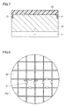
- groove 22a is formed in a lattice pattern as shown in Fig. 8 . That is, groove 22a is formed in a lattice pattern when viewed from above.
- the shape of groove 22a is not particularly limited, and a stripe shape may be employed. It is preferable to form groove 22a on a boundary between the chips, and it is more preferable to form groove 22a along dicing line 3 (see Fig. 1 ) formed in step S 19. In this case, damage to the semiconductor device can be suppressed.
- groove 22a finely partitions mask layer 22 into predetermined areas (e.g., 400 mm 2 ) or less, so that stress can be relaxed. By forming groove 22a, therefore, the warpage of the stacked body including substrate 11, semiconductor layer 12 and mask layer 22 can be reduced.
- a pattern is formed on mask layer 22 (step S6).
- a pattern that opens in a region which is to become well region 13 is formed.
- the pattern can be formed with photolithography, for example. Namely, semiconductor layer 12 having mask layer 22 is set in an exposure device called a stepper, and the mask pattern is transferred, followed by a development process, thereby forming the pattern on mask layer 22.
- step S5 the warpage of the stacked body including substrate 11, semiconductor layer 12 and mask layer 22 is reduced in step S5.
- influence of the warpage can be reduced during the alignment in step S6, thus reducing variation.
- ions are implanted into the region that opens at mask layer 22 having the pattern (step S7).
- an impurity of a p conductivity type e.g., A1
- semiconductor layer 12 is implanted into semiconductor layer 12, thus forming well region 13 as shown in Fig. 10 .
- mask layer 22 is removed.
- step S4 the formation of the mask layer (step S4), the formation of the groove (step S5), the patterning (step S6) and the ion implantation (step S7) are repeated (step S8).
- a new mask layer 24 is formed in order to form source region 14.
- a groove is formed in this mask layer 24 as well. After the groove is formed, patterning is performed to form mask layer 24 having a pattern.
- an impurity of an n conductivity type (e.g., P) is implanted into semiconductor layer 12.
- an activation annealing process may be performed.
- This activation annealing process may be performed with an argon (Ar) gas as an atmospheric gas at a heating temperature of 1700 to 1800°C for a heating period of 30 minutes.
- Ar argon
- Insulating film 15 is formed (step S9).
- Insulating film 15 to be formed has a thickness of 30 nm or more and 100 nm or less, for example.
- insulating film 15 is formed to cover semiconductor layer 12, well region 13, and source layer 14.
- Insulating film 15 may be formed by dry oxidation (thermal oxidation), for example. The dry oxidation may be conducted at a heating temperature of 1200°C for a heating period of 30 minutes.
- insulating film 15 is formed in this step S9, warpage occurs in a stacked body including substrate 11, semiconductor layer 12, and insulating film 15.
- step S 10 a groove (not shown) is formed in insulating film 15 (step S 10). As a result, the warpage generated in insulating film 15 can be reduced.
- annealing with an Ar gas which is inert gas may be performed. Specifically, the annealing may be performed with an Ar gas as an atmospheric gas at a heating temperature of 1100°C for a heating period of 60 minutes.
- surface cleaning such as organic solvent cleaning, acid cleaning or RCA cleaning may be further performed.
- step S11 insulating film 15 is subjected to patterning (step S11). In this step S11, in order to form source electrode 18 on source region 14. insulating film 1 located on the source region is removed.
- gate electrode 16 is formed (step S12). Specifically, a layer made of high-concentration n type poly Si or the like which is to become gate electrode 16 is formed on insulating film 15 with CVD or the like. On this layer, a resist film having a pattern that opens in a region other than a region which is to become gate electrode 16 is formed with photolithography. In order to reduce warpage of the stacked body, a groove may be formed in this resist film as well. With this resist film as a mask, a layer exposed through the pattern is removed with RIE (Reactive Ion Etching) or the like. As a result, gate electrode 16 can be formed.
- RIE Reactive Ion Etching
- source electrode 18 is partially formed (step S13). Specifically, a resist film having a pattern that opens partially in source region 14 is formed with photolithography. A conductor film made of Ni or the like is formed on the pattern and the resist. The resist is then lifted off, to partially form source electrode 18 in contact with source region 14 that opens at insulating film 15.
- drain electrode 19 is formed on a backside of substrate 11 (step S 14).
- Drain electrode 19 may be made of nickel (Ni), for example. After source electrode 18 and drain electrode 19 are formed, alloying heat treatment is performed, for example. As a result, drain electrode 19 can be formed under substrate 11 s shown in Fig. 13 .
- interlayer insulating film 17 is formed (step S15). Specifically, an insulating film made of SiO 2 or the like which is to become interlayer insulating film 17 is formed to cover gate electrode 16.
- a method of forming the insulating film is not particularly limited, and silicon oxide (SiO 2 ), silicon nitride (Si 3 N 4 ) may be deposited with CVD or plasma CVD, for example.
- SiO 2 silicon oxide
- Si 3 N 4 silicon nitride
- 1 ⁇ m of SiO 2 may be deposited by plasma CVD with a source gas of tetraethoxysilane (TEOS) and oxygen (O 2 ) at a heating temperature of 350°C, for example.
- TEOS tetraethoxysilane
- O 2 oxygen
- interlayer insulating film 17 is formed in this step S 11, warpage occurs in a stacked body including substrate 11, semiconductor layer 12, insulating film 15 and gate electrode 16.
- step S 16 groove 2 is formed in interlayer insulating film 17 (step S 16).
- groove 2 is formed in this step S 16, warpage of a stacked body including substrate 11, semiconductor layer 12, insulating film 15, gate electrode 16, partial source electrode 18, and interlayer insulating film 17 can be reduced.
- a method of forming groove 2 is not particularly limited, and can be formed in a manner similar to that of groove 22a in step S5.
- Groove 2 may be formed to penetrate interlayer insulating film 17, or may be formed to not reach the backside. It is preferable to form groove 2 in a lattice pattern in interlayer insulating film 17 to partition the stacked body which is to become chips 10. The remaining configuration of groove 2 is similar to that of groove 22a, and thus description thereof will not be repeated.
- interlayer insulating film 17 is subjected to patterning (step S17).
- a resist film having a pattern that opens in a region other than a region which is to become interlayer insulating film 17 (region where source electrode 18 is to be formed) is formed on interlayer insulating film 17 with photolithography.
- interlayer insulating film 17 exposed through the pattern is removed with RIE or the like.
- a stacked body 20 including interlayer insulating film 17 having the opening, substrate 11, semiconductor layer 12, insulating film 15, and gate electrode 16 can be formed as shown in Fig. 17 .
- source electrode 18 is formed (step S 18). Specifically, an upper source electrode 18 is formed on previously formed partial source electrode 18. Upper source electrode 18 can be formed with lift-off, etching or the like, for example. As a result, the MOSFET as chip 10 shown in Fig. 2 can be manufactured.
- dicing line 3 is formed (step S19). Dicing line 3 partitions the chip into a plurality of chips.
- a method of forming dicing line 3 is not particularly limited, and a mechanical method may be employed, for example.
- semiconductor device 1 shown in Fig. 1 can be manufactured.
- FIGs. 18 to 21 relation between groove 2 formed in interlayer insulating film 17 and dicing line 3 is described.
- Figs. 18 to 21 for the purpose of clarifying the positions of groove 2 and dicing line 3, the remaining configuration that appears when semiconductor device 1 is viewed from above is not illustrated.
- groove 2 may overlap and be narrower than dicing line 3.
- groove 2 may overlap and be wider than dicing line 3.
- groove 2 may be formed to entirely cover dicing line 3.
- the groove for reducing the warpage may be formed in a lattice pattern as shown in Fig. 8 , or in stripes as shown in Fig. 21 , or in a shape to form a plurality of rectangles as shown in Fig. 22 .
- chip 10 has been described as a MOSFET by way of example in this embodiment, chip 10 is not particularly limited as such, but is applicable to a JFET (Junction Field-Effect Transistor), a pn diode, an SBD (Schottky Barrier Diode), an IGBT (Insulated Gate Bipolar Transistor) or the like.
- JFET Joint Field-Effect Transistor
- SBD Schottky Barrier Diode
- IGBT Insulated Gate Bipolar Transistor
- the method of manufacturing semiconductor device 1 in this embodiment includes the step of forming semiconductor layer 12 made of SiC on SiC substrate 11 (step S2), the steps of forming the films on semiconductor layer 12 (steps S4, S9, S15), and the steps of forming the grooves in the films (steps S5, S10, S16).
- the groove is formed in the film formed on semiconductor layer 12 (formed film), rather than in substrate 11 or semiconductor layer 12.
- the present inventors completed the present invention by taking note of warpage resulting from a film formed during the process of manufacturing semiconductor device 1 rather than warpage of substrate 11. Accordingly, warpage resulting from the film can be reduced. As a result, the process of manufacturing semiconductor device 1 can proceed while warpage generated during the process is reduced as appropriate. Moreover, since the warpage is reduced by forming the groove, generated warpage can be reduced regardless of the type of a film. Thus, warpage generated during the process of manufacturing semiconductor device 1 can be reduced. As a result, exposure failure and in-plane variation can be suppressed, thereby manufacturing semiconductor device 1 of improved performance.
- the patterning can be performed with a reduced influence of warpage, thus improving patterning accuracy.
- variation in performance of manufactured semiconductor devices 1 can be suppressed, thereby manufacturing a semiconductor device of improved performance.
- semiconductor device 1 is an SiC semiconductor device
- ions need to be implanted at a high temperature. For this reason, a mask layer needs to have a great thickness. When the mask layer is formed, therefore, warpage tends to occur.
- an SiC semiconductor device is required to have a high breakdown voltage, and thus needs to have a thick insulating film.
- the groove is formed for reducing warpage after the mask layer and the insulating film are formed. Accordingly, if a thick mask layer and a thick insulating film are formed, the process can proceed with a reduced influence of warpage. Therefore, the method of manufacturing semiconductor device 1 in this embodiment is suitable as a method of forming an SiC semiconductor device.
- Semiconductor device 1 in this embodiment including chip 10 having interlayer insulating film 17 includes groove 2 formed in interlayer insulating film 17 to cross chip 10.
- the groove formed in interlayer insulating film 17 reduces warpage generated after interlayer insulating film 17 is formed.
- Semiconductor device 1 is thus manufactured with a reduced influence of warpage, thereby suppressing variation in performance of semiconductor devices 1.
- groove 2 formed between chips 10 can suppress damage to chips 10, thereby realizing semiconductor device 1 of improved performance.
- Samples a to c were made by the following steps. Specifically, first, SiC substrates were prepared. Warpage of the SiC substrate of sample c was measured. The warpage was measured with light interference fringes. The result is shown as "before epitaxial growth" in Fig. 23 . In Fig. 23 , the warpage being 0 means that a measured surface is parallel to a horizontal reference surface.
- the warpage of all of samples a to c could be significantly reduced by forming the groove in the insulating films. It was thus found that warpage generated during a process of manufacturing a semiconductor device can be reduced by forming a groove in a film.
- warpage generated during a process of manufacturing a semiconductor device could be effectively suppressed by providing a step of forming a groove in a film formed on a semiconductor layer. It was also confirmed that, with regard to warpage generated during a process of manufacturing a semiconductor device, warpage generated during the manufacturing process after forming a semiconductor layer had a greater influence than warpage of a semiconductor substrate.
Landscapes
- Electrodes Of Semiconductors (AREA)
- Formation Of Insulating Films (AREA)
Abstract
Description
- The present invention relates to a semiconductor device and a method of manufacturing the semiconductor device.
- Semiconductor devices including silicon carbide (SiC) are conventionally known (e.g., Japanese Patent Laying-Open No.
10-125905 PTL 1 discloses reducing warpage of a semiconductor substrate having an epitaxial layer by performing the following steps. - Specifically, first, an n- type epitaxial layer and a p type epitaxial layer are successively stacked on a surface of an n+ type single-crystal SiC semiconductor substrate, to form an SiC substrate. Then, a plurality of grooves are formed in a surface of the SiC substrate with photolithography. The SiC substrate is then placed in a heater and subjected to heat treatment. Consequently, according to
PTL 1, internal stress generated during formation of the epitaxial layers is relaxed, and the grooves facilitate movement of the surface of the SiC substrate, to correct warpage of the SiC substrate. -
- PTL 1: Japanese Patent Laying-Open No.
10-125905 - In
PTL 1, however, in order to reduce the warpage, the grooves are formed prior to a process of manufacturing a semiconductor device. In general, during a process of manufacturing an SiC semiconductor device, ions are implanted at a high temperature when doping a semiconductor layer with impurities, thus requiring the formation of a thick mask layer. Thus, while the method of manufacturing the semiconductor device described inPTL 1 can correct initial warpage, it is difficult with this method to reduce warpage generated during formation of the mask layer. - In addition, an SiC semiconductor device, which generally has a high breakdown voltage, needs to have a thick insulating film. Thus, with the method of manufacturing the semiconductor device described in
PTL 1, it is difficult to reduce warpage generated during formation of the insulating film. - Furthermore, if warpage generated during a manufacturing process cannot be reduced, performance of a manufactured semiconductor device may be lowered due to exposure failure, in-plane variation and the like.
- Therefore, an object of the present invention is to provide a method of manufacturing a semiconductor device while reducing warpage generated during a process of manufacturing the semiconductor device.
- Another object of the present invention is to provide a semiconductor device of improved performance.
- The present inventors discovered that, when manufacturing a semiconductor device, warpage generated during a process of manufacturing the semiconductor device has a greater influence than warpage of a semiconductor substrate.
- For this reason, a method of manufacturing a semiconductor device of the present invention includes the steps of forming a semiconductor layer made of SiC on an SiC substrate, forming a film on the semiconductor layer, and forming a groove in the film.
- According to the method of manufacturing a semiconductor device of the present invention, the groove is formed in the film formed on the semiconductor layer. Thus, warpage resulting from the film can be reduced. Therefore, warpage generated during a process of manufacturing the semiconductor device can be reduced.
- Preferably, in the above method of manufacturing a semiconductor device, in the step of forming a film, the film is at least one of a mask layer and an insulating film.
- If a mask layer is formed for ion implantation, warpage generated in the semiconductor layer can be reduced by forming the groove in the mask layer. If an insulating film is formed in order to realize a semiconductor device having a high breakdown voltage, warpage generated in the semiconductor layer can be reduced by forming the groove in the insulating film.
- Preferably, in the above method of manufacturing a semiconductor device, in the step of forming a groove, the groove is formed in a lattice pattern.
- Consequently, the groove can be formed readily along a dicing line. Therefore, damage to a chip can be suppressed, and warpage can be reduced during the manufacturing process.
- A semiconductor device of the present invention including a chip having an interlayer insulating film includes a groove formed in the interlayer insulating film to cross the chip.
- According to the semiconductor device of the present invention, the groove formed in the interlayer insulating film reduces warpage when the interlayer insulating film is formed. Since the device is manufactured with a reduced influence of warpage, variation in performance of semiconductor devices can be suppressed. Further, the groove formed between the chips can suppress damage to the chips. Therefore, a semiconductor device of improved performance can be realized.
- As described above, according to the method of manufacturing a semiconductor device of the present invention, a semiconductor device can be manufactured while warpage generated during a process of manufacturing the semiconductor device is reduced. Further, according to the semiconductor device of the present invention, a semiconductor device of improved performance can be realized.
-
-
Fig. 1 is a schematic cross-sectional view of a semiconductor device in an embodiment of the present invention. -
Fig. 2 is a schematic cross-sectional view taken along the line II-II inFig. 1 , schematically showing one chip in the embodiment of the present invention. -
Fig. 3 is a flow chart illustrating a method of manufacturing the semiconductor device in the embodiment of the present invention. -
Fig. 4 is a schematic cross-sectional view for explaining a step in the method of manufacturing the semiconductor device in the embodiment of the present invention. -
Fig. 5 is a schematic cross-sectional view for explaining a step in the method of manufacturing the semiconductor device in the embodiment of the present invention. -
Fig. 6 is a schematic cross-sectional view for explaining a step in the method of manufacturing the semiconductor device in the embodiment of the present invention. -
Fig. 7 is a schematic cross-sectional view for explaining a step in the method of manufacturing the semiconductor device in the embodiment of the present invention, taken along the line VII-VII inFig. 6 . -
Fig. 8 is a schematic cross-sectional view for explaining a step in the method of manufacturing the semiconductor device in the embodiment of the present invention. -
Fig. 9 is a schematic cross-sectional view for explaining a step in the method of manufacturing the semiconductor device in the embodiment of the present invention, taken along the line IX-IX inFig. 8 . -
Fig. 10 is a schematic cross-sectional view for explaining a step in the method of manufacturing the semiconductor device in the embodiment of the present invention. -
Fig. 11 is a schematic cross-sectional view for explaining a step in the method of manufacturing the semiconductor device in the embodiment of the present invention. -
Fig. 12 is a schematic cross-sectional view for explaining a step in the method of manufacturing the semiconductor device in the embodiment of the present invention. -
Fig. 13 is a schematic cross-sectional view for explaining a step in the method of manufacturing the semiconductor device in the embodiment of the present invention. -
Fig. 14 is a schematic cross-sectional view for explaining a step in the method of manufacturing the semiconductor device in the embodiment of the present invention. -
Fig. 15 is a schematic cross-sectional view for explaining a step in the method of manufacturing the semiconductor device in the embodiment of the present invention, taken along the line XV-XV inFig. 14 . -
Fig. 16 is a schematic cross-sectional view for explaining a step in the method of manufacturing the semiconductor device in the embodiment of the present invention. -
Fig. 17 is a schematic cross-sectional view for explaining a step in the method of manufacturing the semiconductor device in the embodiment of the present invention. -
Fig. 18 is a schematic diagram showing relation between a groove and a dicing line of the semiconductor device in the embodiment of the present invention. -
Fig. 19 is a schematic diagram showing relation between the groove and the dicing line of the semiconductor device in the embodiment of the present invention. -
Fig. 20 is a schematic diagram showing relation between the groove and the dicing line of the semiconductor device in the embodiment of the present invention. -
Fig. 21 is a schematic diagram showing a modification of the groove of the semiconductor device in the embodiment of the present invention. -
Fig. 22 is a schematic diagram showing a modification of the groove of the semiconductor device in the embodiment of the present invention. -
Fig. 23 illustrates a warpage state in each process of manufacturing a semiconductor device in the embodiment of the present invention. - An embodiment of the present invention will be described hereinafter with reference to the drawings. It is noted that the same reference numerals are used in the following drawings to indicate the same or corresponding parts, and descriptions thereof will not be repeated.
- Referring to
Figs. 1 and 2 , asemiconductor device 1 in an embodiment of the present invention is described. Referring toFigs. 1 and 2 ,semiconductor device 1 in this embodiment includes achip 10 having an interlayer insulatingfilm 17. A plurality ofchips 10 are partitioned from one another by agroove 2 formed ininterlayer insulating film 17 and adicing line 3.Chips 10 are each a vertical MOSFET (Metal Oxide Semiconductor Field Effect Transistor), for example, as shown inFig. 2 . - As shown in
Fig. 2 , the MOSFET which is onechip 10 includes asubstrate 11, asemiconductor layer 12, awell region 13, asource region 14, an insulatingfilm 15, agate electrode 16,interlayer insulating film 17, asource electrode 18, and adrain electrode 19. -
Substrate 11 is an n type SiC substrate, for example. Formed on thissubstrate 11 issemiconductor layer 12 made of n- SiC, for example. Amark 21 is formed on a main surface ofsemiconductor layer 12. Thismark 21 is an alignment mark used when a mask layer is formed onsemiconductor layer 12. - Well
region 13 is located on part of the main surface ofsemiconductor layer 12 to form a pn junction withsemiconductor layer 12. Wellregion 13 is made of p type SiC, for example.Source region 14 is located on part of a main surface ofwell region 13 to form a pn junction withwell region 13.Source region 14 is made of n+ SiC, for example. -
Semiconductor layer 12 has the same conductivity type (n) as that ofsource region 14, and has a lower impurity concentration than that ofsource region 14.Semiconductor layer 12 has a thickness of 10 µm, for example. The higher or lower level of impurity concentration betweensemiconductor layer 12 andsource region 14 is not particularly limited. It is preferable thatsource region 14 have a higher impurity concentration than that ofsemiconductor layer 12, andsource region 14 has an impurity concentration of 1×1018 cm-3 to 1×1020 cm-3, for example. Nitrogen (N), phosphorus (P) or the like can be used as an n type impurity, for example. - Well
region 13 has a second conductivity type (p) different from that ofsemiconductor layer 12. Aluminum (Al), boron (B) or the like can be used as a p type impurity, for example. Wellregion 13 has an impurity concentration of 5× 1015 cm-3 to 5×1018 cm-3, for example. - A region in
well region 13 sandwiched betweensource region 14 andsemiconductor layer 12 serves as a channel of the MOSFET. While the conductivity types are defined to form an n channel in this embodiment, the first and second conductivity types described above can be reversed to form a p channel. - Insulating film 15 (gate oxide film) is to insulate
semiconductor layer 12 fromgate electrode 16, and is formed in contact with at least a surface ofwell region 13 sandwiched betweensource region 14 andsemiconductor layer 12. Insulatingfilm 15 has a thickness of 30 nm or more and 100 nm or less, for example. -
Gate electrode 16 is formed on insulatingfilm 15 to at least facewell region 13 sandwiched betweensource region 14 andsemiconductor layer 12.Gate electrode 16 may be further formed on another region so long as being formed to face wellregion 13 located betweensource region 14 andsemiconductor layer 12. -
Source electrode 18 is formed onsource region 14 to be electrically connected to sourceregion 14. This source electrode 18 is eclectically isolated fromgate electrode 16 byinterlayer insulating film 17. - As shown in
Fig. 1 ,groove 2 is formed ininterlayer insulating film 17 to crosschip 10 to electrically separate thechip 10 from anotherchip 10. It is preferable thatgroove 2 be formed in a lattice pattern to surround eachchip 10 insemiconductor device 1. - In addition,
drain electrode 19 is formed on a surface ofsubstrate 11 opposite to the surface in contact withsemiconductor layer 12, to be electrically connected tosubstrate 11. - Referring now to
Figs. 1 to 22 , a method ofmanufacturing semiconductor substrate 1 in this embodiment is described. - First, as shown in
Figs. 3 and4 ,substrate 11 is prepared (step S1). In this step S1, an SiC substrate of an n conductivity type is prepared assubstrate 11, for example. Alternatively, an SiC substrate having a specific resistance of 0.02 Ωcm may be used assubstrate 11, for example. - In this step S1, while polishing or the like may be carried out to reduce warpage of
substrate 11 itself, it is preferable to not form a groove insubstrate 11. - Next, as shown in
Figs. 3 and4 ,semiconductor layer 12 made of SiC is formed on substrate 11 (step S2). Specifically, as shown inFig. 4 ,semiconductor layer 12 is formed onsubstrate 11. A method of formingsemiconductor layer 12 is not particularly limited, and CVD (Chemical Vapor Deposition) may be employed, for example.Semiconductor layer 12 is made of SiC of an n conductivity type, for example, and has a thickness of 10 µm, for example. An n type impurity concentration insemiconductor layer 12 may have a value of 1 × 1016 cm-3. for example. - In this step S2, while polishing or the like may be carried out to reduce warpage of a stacked body itself including
substrate 11 andsemiconductor layer 12, it is preferable to not form a groove insemiconductor layer 12. - Next, as shown in
Figs. 3 and5 ,mark 21 is formed (step S3).Mark 21 is an alignment mark used for alignment of a stepper. A method of formingmark 21 is not particularly limited, andsemiconductor layer 12 is irradiated with laser, for example. - Next, as shown in
Figs. 3 ,6 and7 , amask layer 22 is formed on semiconductor layer 12 (step S4).Mask layer 22 is an oxide film, for example. Whenmask layer 22 is formed, warpage occurs in a stackedbody including substrate 11,semiconductor layer 12 andmask layer 22. Furthermore, whenmask layer 22 is formed,mark 21 formed in step S3 becomes less visible. - Next, as shown in
Figs. 3 ,8 and9 , agroove 22a is formed in mask layer 22 (step S5). In this step S5,groove 22a is formed to exposemark 21 ofsemiconductor layer 12. In this embodiment,groove 22a is formed to partition the stacked body which is to become the chips, and to exposemark 21. - In this step S5,
groove 22a is formed in a lattice pattern as shown inFig. 8 . That is,groove 22a is formed in a lattice pattern when viewed from above. The shape ofgroove 22a is not particularly limited, and a stripe shape may be employed. It is preferable to formgroove 22a on a boundary between the chips, and it is more preferable to formgroove 22a along dicing line 3 (seeFig. 1 ) formed instep S 19. In this case, damage to the semiconductor device can be suppressed. - In this step S5,
groove 22a finelypartitions mask layer 22 into predetermined areas (e.g., 400 mm2) or less, so that stress can be relaxed. By forminggroove 22a, therefore, the warpage of the stackedbody including substrate 11,semiconductor layer 12 andmask layer 22 can be reduced. - Next, as shown in
Figs. 3 and10 , a pattern is formed on mask layer 22 (step S6). In this step S6, a pattern that opens in a region which is to becomewell region 13 is formed. The pattern can be formed with photolithography, for example. Namely,semiconductor layer 12 havingmask layer 22 is set in an exposure device called a stepper, and the mask pattern is transferred, followed by a development process, thereby forming the pattern onmask layer 22. - In this embodiment, the warpage of the stacked
body including substrate 11,semiconductor layer 12 andmask layer 22 is reduced in step S5. Thus, influence of the warpage can be reduced during the alignment in step S6, thus reducing variation. - Next, as shown in
Figs. 3 and10 , ions are implanted into the region that opens atmask layer 22 having the pattern (step S7). In this step S7, an impurity of a p conductivity type (e.g., A1) is implanted intosemiconductor layer 12, thus forming wellregion 13 as shown inFig. 10 . After the ion implantation,mask layer 22 is removed. - Next, as shown in
Fig. 3 , the formation of the mask layer (step S4), the formation of the groove (step S5), the patterning (step S6) and the ion implantation (step S7) are repeated (step S8). In this embodiment, as shown inFig. 11 , anew mask layer 24 is formed in order to formsource region 14. In order to reduce warpage, a groove is formed in thismask layer 24 as well. After the groove is formed, patterning is performed to formmask layer 24 having a pattern. - When ions are implanted into a region that opens at
mask layer 24 having the pattern in order to formsource layer 14, an impurity of an n conductivity type (e.g., P) is implanted intosemiconductor layer 12. - After the ion implantation in steps S7 and S8, an activation annealing process may be performed. This activation annealing process may be performed with an argon (Ar) gas as an atmospheric gas at a heating temperature of 1700 to 1800°C for a heating period of 30 minutes. As a result of the activation annealing, the impurity in the ion implantation region can be activated, and crystallinity can be recovered.
- Next, as shown in
Figs. 3 and12 , insulatingfilm 15 is formed (step S9). Insulatingfilm 15 to be formed has a thickness of 30 nm or more and 100 nm or less, for example. - Specifically, as shown in
Fig. 12 , insulatingfilm 15 is formed to coversemiconductor layer 12, wellregion 13, andsource layer 14. Insulatingfilm 15 may be formed by dry oxidation (thermal oxidation), for example. The dry oxidation may be conducted at a heating temperature of 1200°C for a heating period of 30 minutes. - When insulating
film 15 is formed in this step S9, warpage occurs in a stackedbody including substrate 11,semiconductor layer 12, and insulatingfilm 15. - Next, as shown in
Fig. 3 , a groove (not shown) is formed in insulating film 15 (step S 10). As a result, the warpage generated in insulatingfilm 15 can be reduced. - After step S9 or
S 10, annealing with an Ar gas which is inert gas, for example, may be performed. Specifically, the annealing may be performed with an Ar gas as an atmospheric gas at a heating temperature of 1100°C for a heating period of 60 minutes. - Subsequently, surface cleaning such as organic solvent cleaning, acid cleaning or RCA cleaning may be further performed.
- Next, as shown in
Figs. 3 and13 , insulatingfilm 15 is subjected to patterning (step S11). In this step S11, in order to formsource electrode 18 onsource region 14. insulatingfilm 1 located on the source region is removed. - Next, as shown in
Figs. 3 and13 ,gate electrode 16 is formed (step S12). Specifically, a layer made of high-concentration n type poly Si or the like which is to becomegate electrode 16 is formed on insulatingfilm 15 with CVD or the like. On this layer, a resist film having a pattern that opens in a region other than a region which is to becomegate electrode 16 is formed with photolithography. In order to reduce warpage of the stacked body, a groove may be formed in this resist film as well. With this resist film as a mask, a layer exposed through the pattern is removed with RIE (Reactive Ion Etching) or the like. As a result,gate electrode 16 can be formed. - Next, as shown in
Figs. 3 and13 ,source electrode 18 is partially formed (step S13). Specifically, a resist film having a pattern that opens partially insource region 14 is formed with photolithography. A conductor film made of Ni or the like is formed on the pattern and the resist. The resist is then lifted off, to partially formsource electrode 18 in contact withsource region 14 that opens at insulatingfilm 15. - In addition,
drain electrode 19 is formed on a backside of substrate 11 (step S 14).Drain electrode 19 may be made of nickel (Ni), for example. Aftersource electrode 18 anddrain electrode 19 are formed, alloying heat treatment is performed, for example. As a result,drain electrode 19 can be formed under substrate 11 s shown inFig. 13 . - Next, as shown in
Figs. 3 ,14 and15 ,interlayer insulating film 17 is formed (step S15). Specifically, an insulating film made of SiO2 or the like which is to become interlayer insulatingfilm 17 is formed to covergate electrode 16. A method of forming the insulating film is not particularly limited, and silicon oxide (SiO2), silicon nitride (Si3N4) may be deposited with CVD or plasma CVD, for example. For example, 1 µm of SiO2 may be deposited by plasma CVD with a source gas of tetraethoxysilane (TEOS) and oxygen (O2) at a heating temperature of 350°C, for example. - When interlayer insulating
film 17 is formed in this step S 11, warpage occurs in a stackedbody including substrate 11,semiconductor layer 12, insulatingfilm 15 andgate electrode 16. - Next, as shown in
Figs. 3 and16 ,groove 2 is formed in interlayer insulating film 17 (step S 16). By forminggroove 2 in this step S 16, warpage of a stackedbody including substrate 11,semiconductor layer 12, insulatingfilm 15,gate electrode 16,partial source electrode 18, andinterlayer insulating film 17 can be reduced. - A method of forming
groove 2 is not particularly limited, and can be formed in a manner similar to that ofgroove 22a in step S5.Groove 2 may be formed to penetrateinterlayer insulating film 17, or may be formed to not reach the backside. It is preferable to formgroove 2 in a lattice pattern ininterlayer insulating film 17 to partition the stacked body which is to becomechips 10. The remaining configuration ofgroove 2 is similar to that ofgroove 22a, and thus description thereof will not be repeated. - Next, as shown in
Figs. 3 and17 ,interlayer insulating film 17 is subjected to patterning (step S17). In this step S17, a resist film having a pattern that opens in a region other than a region which is to become interlayer insulating film 17 (region where source electrode 18 is to be formed) is formed oninterlayer insulating film 17 with photolithography. With this resist film as a mask,interlayer insulating film 17 exposed through the pattern is removed with RIE or the like. As a result, astacked body 20 includinginterlayer insulating film 17 having the opening,substrate 11,semiconductor layer 12, insulatingfilm 15, andgate electrode 16 can be formed as shown inFig. 17 . - Next, as shown in
Figs. 2 and3 ,source electrode 18 is formed (step S 18). Specifically, anupper source electrode 18 is formed on previously formedpartial source electrode 18.Upper source electrode 18 can be formed with lift-off, etching or the like, for example. As a result, the MOSFET aschip 10 shown inFig. 2 can be manufactured. - Next, as shown in
Figs. 1 and3 , dicingline 3 is formed (step S19).Dicing line 3 partitions the chip into a plurality of chips. A method of formingdicing line 3 is not particularly limited, and a mechanical method may be employed, for example. - By performing above
steps S 1 to S19,semiconductor device 1 shown inFig. 1 can be manufactured. - Referring now to
Figs. 18 to 21 , relation betweengroove 2 formed ininterlayer insulating film 17 anddicing line 3 is described. InFigs. 18 to 21 , for the purpose of clarifying the positions ofgroove 2 anddicing line 3, the remaining configuration that appears whensemiconductor device 1 is viewed from above is not illustrated. - As shown in
Fig. 18 ,groove 2 may overlap and be narrower than dicingline 3. Alternatively, as shown inFig. 19 ,groove 2 may overlap and be wider than dicingline 3. Alternatively, as shown inFig. 20 ,groove 2 may be formed to entirely coverdicing line 3. - The groove for reducing the warpage may be formed in a lattice pattern as shown in
Fig. 8 , or in stripes as shown inFig. 21 , or in a shape to form a plurality of rectangles as shown inFig. 22 . - While one
chip 10 is formed in a region surrounded bygroove 2 formed ininterlayer insulating film 17 in this embodiment, a plurality ofchips 10 may be formed therein. - While
chip 10 has been described as a MOSFET by way of example in this embodiment,chip 10 is not particularly limited as such, but is applicable to a JFET (Junction Field-Effect Transistor), a pn diode, an SBD (Schottky Barrier Diode), an IGBT (Insulated Gate Bipolar Transistor) or the like. - As described above, the method of
manufacturing semiconductor device 1 in this embodiment includes the step of formingsemiconductor layer 12 made of SiC on SiC substrate 11 (step S2), the steps of forming the films on semiconductor layer 12 (steps S4, S9, S15), and the steps of forming the grooves in the films (steps S5, S10, S16). - According to the method of
manufacturing semiconductor device 1 of the present invention, the groove is formed in the film formed on semiconductor layer 12 (formed film), rather than insubstrate 11 orsemiconductor layer 12. The present inventors completed the present invention by taking note of warpage resulting from a film formed during the process ofmanufacturing semiconductor device 1 rather than warpage ofsubstrate 11. Accordingly, warpage resulting from the film can be reduced. As a result, the process ofmanufacturing semiconductor device 1 can proceed while warpage generated during the process is reduced as appropriate. Moreover, since the warpage is reduced by forming the groove, generated warpage can be reduced regardless of the type of a film. Thus, warpage generated during the process ofmanufacturing semiconductor device 1 can be reduced. As a result, exposure failure and in-plane variation can be suppressed, thereby manufacturingsemiconductor device 1 of improved performance. - In particular, since the warpage resulting from the film formation is reduced prior to patterning, the patterning can be performed with a reduced influence of warpage, thus improving patterning accuracy. As a result, variation in performance of manufactured
semiconductor devices 1 can be suppressed, thereby manufacturing a semiconductor device of improved performance. - Moreover, since the groove is not directly formed in
substrate 11 andsemiconductor layer 12, damage tosubstrate 11 andsemiconductor layer 12 can be suppressed. - Furthermore, since
semiconductor device 1 is an SiC semiconductor device, ions need to be implanted at a high temperature. For this reason, a mask layer needs to have a great thickness. When the mask layer is formed, therefore, warpage tends to occur. Likewise, an SiC semiconductor device is required to have a high breakdown voltage, and thus needs to have a thick insulating film. In this embodiment, however, the groove is formed for reducing warpage after the mask layer and the insulating film are formed. Accordingly, if a thick mask layer and a thick insulating film are formed, the process can proceed with a reduced influence of warpage. Therefore, the method ofmanufacturing semiconductor device 1 in this embodiment is suitable as a method of forming an SiC semiconductor device. -
Semiconductor device 1 in thisembodiment including chip 10 havinginterlayer insulating film 17 includesgroove 2 formed ininterlayer insulating film 17 to crosschip 10. - According to
semiconductor device 1 in this embodiment, the groove formed ininterlayer insulating film 17 reduces warpage generated after interlayer insulatingfilm 17 is formed.Semiconductor device 1 is thus manufactured with a reduced influence of warpage, thereby suppressing variation in performance ofsemiconductor devices 1. Further,groove 2 formed betweenchips 10 can suppress damage tochips 10, thereby realizingsemiconductor device 1 of improved performance. - In this example, the effect of providing a step of forming a groove in a film formed on a semiconductor layer was examined.
- Samples a to c were made by the following steps. Specifically, first, SiC substrates were prepared. Warpage of the SiC substrate of sample c was measured. The warpage was measured with light interference fringes. The result is shown as "before epitaxial growth" in
Fig. 23 . InFig. 23 , the warpage being 0 means that a measured surface is parallel to a horizontal reference surface. - Next, a semiconductor layer made of SiC was formed on the SiC substrates. Warpage of samples a to c after forming the semiconductor layer was measured in a manner similar to above. The results are shown as "after epitaxial growth" in
Fig. 23 . - Next, an insulating film made of SiO2 was formed on the semiconductor layers. Warpage of samples a to c after forming the insulating film was measured in a manner similar to above. The results are shown as "film stacking" in
Fig. 23 . - Next, a groove in a lattice pattern having a width of 100 µm was formed in the insulating films. Warpage of samples a to c after forming the groove was measured in a manner similar to above. The results are shown as "film partitioning" in
Fig. 23 . - As shown in
Fig. 23 , the warpage of all of samples a to c could be significantly reduced by forming the groove in the insulating films. It was thus found that warpage generated during a process of manufacturing a semiconductor device can be reduced by forming a groove in a film. - In addition, referring to sample c, it was found that the warpage generated when the insulating film was formed was much more greater than the warpage generated when the semiconductor layer made of SiC was formed on the SiC substrate. It was thus found that deterioration in performance of a semiconductor device can be suppressed by reducing warpage generated when an insulating film is formed.
- Based on the above findings, according to this example, it was confirmed that warpage generated during a process of manufacturing a semiconductor device could be effectively suppressed by providing a step of forming a groove in a film formed on a semiconductor layer. It was also confirmed that, with regard to warpage generated during a process of manufacturing a semiconductor device, warpage generated during the manufacturing process after forming a semiconductor layer had a greater influence than warpage of a semiconductor substrate.
- Although the embodiments and examples of the present invention have been described above, it is also originally intended to combine the features of the embodiments and examples as appropriate. Moreover, it should be understood that the embodiments and examples disclosed herein are illustrative and non-restrictive in every respect. The scope of the present invention is defined by the terms of the claims, rather than the description above, and is intended to include any modifications within the scope and meaning equivalent to the terms of the claims.
- 1 semiconductor device; 2 groove; 3 dicing line; 10 chip; 11 substrate; 12 semiconductor layer; 13 well region; 14 source region; 15 insulating film; 16 gate electrode; 17 interlayer insulating film; 18 source electrode; 19 drain electrode; 20 stacked body; 21 mark; 22, 24 mask layer; 22a groove.
Claims (4)
- A method of manufacturing a semiconductor device (1), comprising the steps of:forming a semiconductor layer (12) made of silicon carbide on a silicon carbide substrate (11);forming a film on said semiconductor layer (12); andforming a groove in said film.
- The method of manufacturing a semiconductor device (1) according to claim 1, wherein
in said step of forming a film, said film is at least one of a mask layer (22, 24) and an insulating film (15, 17). - The method of manufacturing a semiconductor device (1) according to claim 1, wherein
in said step of forming a groove, said groove is formed in a lattice pattern. - A semiconductor device (1) including a chip (10) having an interlayer insulating film (17), comprising a groove (2) formed in said interlayer insulating film (17) to cross said chip (10).
Applications Claiming Priority (2)
| Application Number | Priority Date | Filing Date | Title |
|---|---|---|---|
| JP2009207206A JP2011060901A (en) | 2009-09-08 | 2009-09-08 | Semiconductor device, and semiconductor device manufacturing method |
| PCT/JP2010/064213 WO2011030661A1 (en) | 2009-09-08 | 2010-08-24 | Semiconductor device and process for production of semiconductor device |
Publications (2)
| Publication Number | Publication Date |
|---|---|
| EP2477213A1 true EP2477213A1 (en) | 2012-07-18 |
| EP2477213A4 EP2477213A4 (en) | 2014-05-14 |
Family
ID=43732335
Family Applications (1)
| Application Number | Title | Priority Date | Filing Date |
|---|---|---|---|
| EP10815258.8A Withdrawn EP2477213A4 (en) | 2009-09-08 | 2010-08-24 | SEMICONDUCTOR DEVICE AND METHOD FOR PRODUCING SEMICONDUCTOR DEVICE |
Country Status (8)
| Country | Link |
|---|---|
| US (1) | US20120171850A1 (en) |
| EP (1) | EP2477213A4 (en) |
| JP (1) | JP2011060901A (en) |
| KR (1) | KR20120067340A (en) |
| CN (1) | CN102484075A (en) |
| CA (1) | CA2772676A1 (en) |
| TW (1) | TW201130046A (en) |
| WO (1) | WO2011030661A1 (en) |
Cited By (1)
| Publication number | Priority date | Publication date | Assignee | Title |
|---|---|---|---|---|
| WO2021028353A1 (en) | 2019-08-09 | 2021-02-18 | Abb Schweiz Ag | Strain enhanced sic power semiconductor device and method of manufacturing |
Families Citing this family (7)
| Publication number | Priority date | Publication date | Assignee | Title |
|---|---|---|---|---|
| US9420694B2 (en) * | 2010-08-31 | 2016-08-16 | Ge Embedded Electronics Oy | Method for controlling warpage within electronic products and an electronic product |
| CN102436133A (en) * | 2011-08-17 | 2012-05-02 | 上海华力微电子有限公司 | Method for preventing movement of main graphics caused by stress transferred by photomask version |
| CN102436134A (en) * | 2011-08-29 | 2012-05-02 | 上海华力微电子有限公司 | Method for preventing photomask from being damaged by stress in non-light-transmitting cutting channel |
| JP6887244B2 (en) * | 2016-12-09 | 2021-06-16 | ルネサスエレクトロニクス株式会社 | Semiconductor devices and their manufacturing methods |
| US10998418B2 (en) * | 2019-05-16 | 2021-05-04 | Cree, Inc. | Power semiconductor devices having reflowed inter-metal dielectric layers |
| DE102019120692B4 (en) * | 2019-07-31 | 2025-12-11 | Infineon Technologies Ag | Power semiconductor device and method |
| CN117976698A (en) * | 2024-03-28 | 2024-05-03 | 南京第三代半导体技术创新中心有限公司 | High reliability planar gate silicon carbide MOSFET power device and manufacturing method thereof |
Family Cites Families (24)
| Publication number | Priority date | Publication date | Assignee | Title |
|---|---|---|---|---|
| JPH10125905A (en) * | 1996-10-17 | 1998-05-15 | Denso Corp | Semiconductor substrate and method of straightening semiconductor substrate |
| US7282739B2 (en) * | 2002-04-26 | 2007-10-16 | Nissan Motor Co., Ltd. | Silicon carbide semiconductor device |
| JP2003332270A (en) * | 2002-05-15 | 2003-11-21 | Renesas Technology Corp | Semiconductor device and method of manufacturing the same |
| JP4303917B2 (en) * | 2002-06-05 | 2009-07-29 | パナソニック株式会社 | Manufacturing method of semiconductor device |
| KR20050001717A (en) * | 2003-06-26 | 2005-01-07 | 주식회사 하이닉스반도체 | Method for trench type isolation in semiconductor device |
| US7407837B2 (en) * | 2004-01-27 | 2008-08-05 | Fuji Electric Holdings Co., Ltd. | Method of manufacturing silicon carbide semiconductor device |
| JP4237086B2 (en) * | 2004-03-22 | 2009-03-11 | 関西電力株式会社 | Voltage-controlled semiconductor device |
| US7355207B2 (en) * | 2004-05-24 | 2008-04-08 | Denso Corporation | Silicon carbide semiconductor device and method for manufacturing the same |
| JP2005337956A (en) * | 2004-05-28 | 2005-12-08 | Yamaha Corp | Physical quantity sensor and manufacturing method therefor |
| WO2007023950A1 (en) * | 2005-08-26 | 2007-03-01 | Hitachi, Ltd. | Semiconductor device manufacturing method |
| EP1850396A3 (en) * | 2006-04-28 | 2008-09-17 | Nissan Motor Co., Ltd. | Semiconductor device and manufacturing method thereof |
| JP4710724B2 (en) * | 2006-06-07 | 2011-06-29 | 株式会社デンソー | Manufacturing method of semiconductor device |
| JP2008053363A (en) * | 2006-08-23 | 2008-03-06 | Matsushita Electric Ind Co Ltd | Semiconductor substrate and manufacturing method thereof |
| JP5018044B2 (en) * | 2006-11-28 | 2012-09-05 | パナソニック株式会社 | Semiconductor device manufacturing substrate |
| JP4899829B2 (en) * | 2006-11-30 | 2012-03-21 | パナソニック株式会社 | Semiconductor device manufacturing substrate |
| JP5509520B2 (en) * | 2006-12-21 | 2014-06-04 | 富士電機株式会社 | Method for manufacturing silicon carbide semiconductor device |
| JP2008244455A (en) * | 2007-02-28 | 2008-10-09 | Denso Corp | Silicon carbide semiconductor device and manufacturing method thereof |
| JP4331773B2 (en) * | 2007-03-20 | 2009-09-16 | Okiセミコンダクタ株式会社 | Semiconductor device and manufacturing method thereof |
| JP2007201499A (en) * | 2007-04-06 | 2007-08-09 | Denso Corp | Semiconductor substrate and manufacturing method thereof |
| US7820534B2 (en) * | 2007-08-10 | 2010-10-26 | Mitsubishi Electric Corporation | Method of manufacturing silicon carbide semiconductor device |
| JP2009054718A (en) * | 2007-08-24 | 2009-03-12 | Fuji Electric Device Technology Co Ltd | Manufacturing method of semiconductor device |
| JP5141227B2 (en) * | 2007-12-12 | 2013-02-13 | 住友電気工業株式会社 | Manufacturing method of semiconductor device |
| JP2009182271A (en) * | 2008-01-31 | 2009-08-13 | Toshiba Corp | Silicon carbide semiconductor device |
| JP4640439B2 (en) * | 2008-04-17 | 2011-03-02 | 株式会社デンソー | Silicon carbide semiconductor device |
-
2009
- 2009-09-08 JP JP2009207206A patent/JP2011060901A/en active Pending
-
2010
- 2010-08-24 CN CN2010800398076A patent/CN102484075A/en active Pending
- 2010-08-24 CA CA2772676A patent/CA2772676A1/en not_active Abandoned
- 2010-08-24 KR KR1020127006763A patent/KR20120067340A/en not_active Withdrawn
- 2010-08-24 WO PCT/JP2010/064213 patent/WO2011030661A1/en not_active Ceased
- 2010-08-24 EP EP10815258.8A patent/EP2477213A4/en not_active Withdrawn
- 2010-08-24 US US13/394,770 patent/US20120171850A1/en not_active Abandoned
- 2010-09-03 TW TW099129938A patent/TW201130046A/en unknown
Cited By (2)
| Publication number | Priority date | Publication date | Assignee | Title |
|---|---|---|---|---|
| WO2021028353A1 (en) | 2019-08-09 | 2021-02-18 | Abb Schweiz Ag | Strain enhanced sic power semiconductor device and method of manufacturing |
| US12113131B2 (en) | 2019-08-09 | 2024-10-08 | Hitachi Energy Ltd | Strain enhanced SiC power semiconductor device and method of manufacturing |
Also Published As
| Publication number | Publication date |
|---|---|
| JP2011060901A (en) | 2011-03-24 |
| KR20120067340A (en) | 2012-06-25 |
| CN102484075A (en) | 2012-05-30 |
| EP2477213A4 (en) | 2014-05-14 |
| WO2011030661A1 (en) | 2011-03-17 |
| CA2772676A1 (en) | 2011-03-17 |
| TW201130046A (en) | 2011-09-01 |
| US20120171850A1 (en) | 2012-07-05 |
Similar Documents
| Publication | Publication Date | Title |
|---|---|---|
| EP2477213A1 (en) | Semiconductor device and process for production of semiconductor device | |
| JP5525940B2 (en) | Semiconductor device and manufacturing method of semiconductor device | |
| US8564017B2 (en) | Silicon carbide semiconductor device and method for manufacturing same | |
| EP3667736A1 (en) | Semiconductor device and manufacturing method for same | |
| EP2927939A1 (en) | Silicon carbide semiconductor device, and manufacturing method for same | |
| US8847238B2 (en) | Semiconductor device which can withstand high voltage or high current and method for fabricating the same | |
| US20150287817A1 (en) | Silicon carbide semiconductor device and method for manufacturing same | |
| JP7146018B2 (en) | semiconductor equipment | |
| JP6991476B2 (en) | Semiconductor device | |
| US9653297B2 (en) | Method of manufacturing silicon carbide semiconductor device by forming metal-free protection film | |
| US10424637B2 (en) | Method of manufacturing semiconductor device | |
| CN111326584B (en) | Silicon carbide MOSFET and preparation method thereof | |
| CN118511283A (en) | Silicon carbide semiconductor device and method for manufacturing silicon carbide semiconductor device | |
| US8796123B2 (en) | Method of manufacturing silicon carbide semiconductor device | |
| CN113903800B (en) | Semiconductor devices | |
| US20240290616A1 (en) | Silicon carbide semiconductor device and manufacturing method of the same | |
| US20260101573A1 (en) | Semiconductor device and method of manufacturing semiconductor device | |
| US9966437B2 (en) | Method for manufacturing silicon carbide semiconductor device | |
| US20250212444A1 (en) | Semiconductor device and method for manufacturing the same | |
| US20260068206A1 (en) | Method of manufacturing semiconductor device | |
| CN116230740A (en) | Super-junction IGBT device with carrier storage layer and manufacturing method thereof | |
| JP2020043196A (en) | Silicon carbide semiconductor device |
Legal Events
| Date | Code | Title | Description |
|---|---|---|---|
| PUAI | Public reference made under article 153(3) epc to a published international application that has entered the european phase |
Free format text: ORIGINAL CODE: 0009012 |
|
| 17P | Request for examination filed |
Effective date: 20120330 |
|
| AK | Designated contracting states |
Kind code of ref document: A1 Designated state(s): AL AT BE BG CH CY CZ DE DK EE ES FI FR GB GR HR HU IE IS IT LI LT LU LV MC MK MT NL NO PL PT RO SE SI SK SM TR |
|
| DAX | Request for extension of the european patent (deleted) | ||
| A4 | Supplementary search report drawn up and despatched |
Effective date: 20140414 |
|
| RIC1 | Information provided on ipc code assigned before grant |
Ipc: H01L 29/16 20060101ALI20140408BHEP Ipc: H01L 29/66 20060101ALI20140408BHEP Ipc: H01L 29/12 20060101ALI20140408BHEP Ipc: H01L 23/544 20060101AFI20140408BHEP Ipc: H01L 21/336 20060101ALI20140408BHEP Ipc: H01L 29/78 20060101ALI20140408BHEP |
|
| STAA | Information on the status of an ep patent application or granted ep patent |
Free format text: STATUS: THE APPLICATION HAS BEEN WITHDRAWN |
|
| 18W | Application withdrawn |
Effective date: 20140618 |