EP2476644A2 - Method of making a MEMS device - Google Patents
Method of making a MEMS device Download PDFInfo
- Publication number
- EP2476644A2 EP2476644A2 EP11184861A EP11184861A EP2476644A2 EP 2476644 A2 EP2476644 A2 EP 2476644A2 EP 11184861 A EP11184861 A EP 11184861A EP 11184861 A EP11184861 A EP 11184861A EP 2476644 A2 EP2476644 A2 EP 2476644A2
- Authority
- EP
- European Patent Office
- Prior art keywords
- layer
- mems device
- etching
- metal layer
- forming
- Prior art date
- Legal status (The legal status is an assumption and is not a legal conclusion. Google has not performed a legal analysis and makes no representation as to the accuracy of the status listed.)
- Granted
Links
Images


Classifications
-
- B—PERFORMING OPERATIONS; TRANSPORTING
- B81—MICROSTRUCTURAL TECHNOLOGY
- B81C—PROCESSES OR APPARATUS SPECIALLY ADAPTED FOR THE MANUFACTURE OR TREATMENT OF MICROSTRUCTURAL DEVICES OR SYSTEMS
- B81C1/00—Manufacture or treatment of devices or systems in or on a substrate
- B81C1/00777—Preserve existing structures from alteration, e.g. temporary protection during manufacturing
- B81C1/00785—Avoid chemical alteration, e.g. contamination, oxidation or unwanted etching
- B81C1/00801—Avoid alteration of functional structures by etching, e.g. using a passivation layer or an etch stop layer
-
- B—PERFORMING OPERATIONS; TRANSPORTING
- B81—MICROSTRUCTURAL TECHNOLOGY
- B81C—PROCESSES OR APPARATUS SPECIALLY ADAPTED FOR THE MANUFACTURE OR TREATMENT OF MICROSTRUCTURAL DEVICES OR SYSTEMS
- B81C1/00—Manufacture or treatment of devices or systems in or on a substrate
-
- B—PERFORMING OPERATIONS; TRANSPORTING
- B81—MICROSTRUCTURAL TECHNOLOGY
- B81B—MICROSTRUCTURAL DEVICES OR SYSTEMS, e.g. MICROMECHANICAL DEVICES
- B81B3/00—Devices comprising flexible or deformable elements, e.g. comprising elastic tongues or membranes
-
- G—PHYSICS
- G01—MEASURING; TESTING
- G01C—MEASURING DISTANCES, LEVELS OR BEARINGS; SURVEYING; NAVIGATION; GYROSCOPIC INSTRUMENTS; PHOTOGRAMMETRY OR VIDEOGRAMMETRY
- G01C19/00—Gyroscopes; Turn-sensitive devices using vibrating masses; Turn-sensitive devices without moving masses; Measuring angular rate using gyroscopic effects
- G01C19/56—Turn-sensitive devices using vibrating masses, e.g. vibratory angular rate sensors based on Coriolis forces
-
- B—PERFORMING OPERATIONS; TRANSPORTING
- B81—MICROSTRUCTURAL TECHNOLOGY
- B81B—MICROSTRUCTURAL DEVICES OR SYSTEMS, e.g. MICROMECHANICAL DEVICES
- B81B2207/00—Microstructural systems or auxiliary parts thereof
- B81B2207/07—Interconnects
-
- B—PERFORMING OPERATIONS; TRANSPORTING
- B81—MICROSTRUCTURAL TECHNOLOGY
- B81C—PROCESSES OR APPARATUS SPECIALLY ADAPTED FOR THE MANUFACTURE OR TREATMENT OF MICROSTRUCTURAL DEVICES OR SYSTEMS
- B81C2201/00—Manufacture or treatment of microstructural devices or systems
- B81C2201/05—Temporary protection of devices or parts of the devices during manufacturing
- B81C2201/053—Depositing a protective layers
Definitions
- This disclosure relates generally to MEMS devices, and more specifically, to methods of making MEMS devices.
- Micro-electro-mechanical-systems are finding more and more uses, especially for spatial sensing uses such accelerometers, position detectors, and gyroscopes. These functions are becoming more and more common and finding uses in many consumers devices such as mobile phones, automobiles, and electronic games. As the uses increase the demand for lower cost also increases which bears on having manufacturing processes that provide sufficient quality at high volume.
- One of the things that is typically involved with a MEMS device is a portion that has some freedom of movement, often in 3 axes. The manufacturing of this portion is critical to the functionality of the MEMS device. Integrating this key process with other features that must also be present presents difficulties.
- FIG. 1 is a cross section of a MEMS device at a stage in processing according to a first embodiment
- FIG. 2 is a cross section of the MEMS device of FIG. 1 at a subsequent stage in processing
- FIG. 3 is a cross section of the MEMS device of FIG. 2 at a subsequent stage in processing
- FIG. 4 is a cross section of the MEMS device of FIG. 3 at a subsequent stage in processing
- FIG. 5 is a cross section of the MEMS device of FIG. 4 at a subsequent stage in processing
- FIG. 6 is a cross section of the MEMS device of FIG. 5 at a subsequent stage in processing
- FIG. 7 is a cross section of the MEMS device of FIG. 6 at a subsequent stage in processing
- FIG. 8 is a cross section of the MEMS device of FIG. 7 at a subsequent stage in processing
- FIG. 9 is a cross section of a MEMS device at a stage in processing according to a second embodiment
- FIG. 10 is a cross section of the MEMS device of FIG. 9 at a subsequent stage in processing.
- FIG. 11 is a cross section of the MEMS device of FIG. 10 at a subsequent stage in processing.
- a micro-electro-mechanical-systems (MEMS) device is made using an etch that provides freedom of motion of a polysilicon member while protecting a contact pad from the etchants used to perform the etch that provides the freedom of motion.
- the protection is achieved by depositing a sacrificial layer and patterning it to leave a portion over the location of the contact pad.
- the etch tends to leave a layer on the contact pad, if it is unprotected, that makes it difficult to adhere a wire bond or other contacting material.
- the etch is very significant to the freedom of motion and thus is very important to control in order to achieve the needed performance of the MEMS device.
- the remaining portion of the sacrificial layer is removed after the etch to make the contact available for contacting. This is better understood by reference to the drawings and the following specification.
- the semiconductor substrate described herein can be any semiconductor material or combinations of materials, such as gallium arsenide, silicon germanium, silicon-on-insulator (SOI), silicon, monocrystalline silicon, the like, and combinations of the above.
- SOI silicon-on-insulator
- FIG. 1 Shown in FIG. 1 is a MEMS device 10 comprising a substrate 12; a thermal oxide layer 14 grown on substrate 14; a patterned polysilicon layer having polysilicon portions 16 18, and 22; a silicon nitride layer on polysilicon portions 16, 18, and 22 and on thermal oxide layer 14 having nitride portion 24 on polysilicon portion 16 and thermal oxide layer 14, nitride portion 26 on polysilicon portion 18, and nitride portion 28 on polysilicon portion 22 and thermal oxide layer 14; a deposited oxide layer having an oxide portion 30 on nitride portion 24, an oxide portion 32 on nitride portion 26, and an oxide portion 34 on nitride portion 28; a polysilicon layer 36 over oxide portions 30, 32, and 34 and thermal oxide layer 14; a deposited oxide layer over polysilicon layer 36 having an oxide portion 38 and an oxide portion 40; and a metal layer 42 over deposited oxide layer 40 and polysilicon layer 36.
- a region 31 of polysilicon layer 36 is between oxide portions 30 and 32, between nitride portions 24 and 26, and between polysilicon portions 16 and 18.
- a region 33 of polysilicon layer 36 is between oxide portions 32 and 34, between nitride portions 26 and 28, and between polysilicon portions 18 and 22.
- a region 35 of metal layer is between oxide portions 38 and 40. Effective thicknesses for the various layers are as follows: 2.5 microns for thermal oxide 14; 0.35 micron for polysilicon portions 16, 18, and 22; 0.3 micron for nitride portions 24, 26, and 28; 1.8 microns for oxide portions 30, 32, and 34; 25 microns for polysilicon layer 36; 0.4 micron for oxide portions 38 and 40; and 1.4 microns for metal layer 35. Other dimensions will work as well.
- Metal layer 42 may comprise aluminum and may include other materials as well such as copper and silicon.
- Oxide portions 30, 32, and 34 are preferably deposited using tetraethylorthosilicate (TEOS) but other techniques may also be effective.
- TEOS tetraethylorthosilicate
- the various polysilicon layers may be doped. Polysilicon portion 18 should be conductive so if polyslicon is chosen for this purpose it should be doped.
- SiRN layer 44 Shown in FIG. 2 is MEMS device 10 after depositing a silicon-rich silicon nitride (SiRN) layer 44 that may have a thickness of 0.75 micron.
- SiRN layer 44 may have refractive index of 2.19. Other relative concentrations of silicon resulting in a lower or higher refractive index may also be effective.
- Stoichemetric silicon nitride has about a 2.02 refractive index. Thus it is desirable that the refractive index exceed 2.02.
- SiRN is preferable to stoichemetric silicon nitride because, for hydrofluoric acid (HF) in vapor form, silicon-rich silicon nitride etches more slowly.
- HF hydrofluoric acid
- SiRN is the preferred material, other materials may also be effective for layer 44. Exemplary materials are titanium nitride, titanium, and amorphous carbide. Other materials may also be effective.
- layer 44 may be a conductor or a dielectric.
- MEMS device 10 Shown in FIG. 3 is MEMS device 10 after performing a patterned etch of metal layer 42 and SiRN layer 44 aligned to region 35 and thus leaving region 35 of metal layer 42 and the portion of SiRN layer 44 aligned to region 31.
- MEMS device 10 Shown in FIG. 4 is MEMS device 10 after depositing a layer 46 of oxide having a thickness that may be 0.4 micron.
- FIG. 5 Shown in FIG. 5 is MEMS device 10 after etching openings 48, 50, and 52 through oxide layer 46, oxide layer 40, and polysilicon layer 36 to expose portions of oxide portions 30, 32, and 34. Opening 48 surrounds a contact stack 54. Openings 50 and 52 are such that the portions of polysilicon layer 36 adjacent to openings 50 and 52 remain as part of a continuous portion of polysilicon layer 36. This will be the movable member of the MEMS device which may also be called the movable portion of the MEMS device.
- FIG. 6 Shown in FIG. 6 is MEMS device after an oxide etch using vapor phase HF which removes oxide portions 30, 32, and 34 as well as oxide layers 46 and 40.
- Oxide portions 30, 32, and 34 may be considered sacrificial.
- SiRN layer 44 functions as an etch stop so that metal layer 42 does not receive the HF etch and is thus a protection layer as it protects metal layer 42.
- SiRN layer 44 is also etched but the vapor phase HF etch is tuned so that the oxide is etched much faster than SiRN. A consequence of this etch is residue 58 on nitride portions 24, 26, and 28 and a residue 56 on SiRN layer 44.
- the removal of oxide portions 32 and 34 has the effect of releasing the movable member portion of polysilicon layer 36 to be movable.
- Region 33 functions as a base for the movable member portion of polysilicon layer 36.
- the portion of polysilicon layer 36 that is part of contact stack 54 makes contact to polysilicon portion 18 which in turn contacts the movable member at region 33.
- the HF etch if it contacts metal layer 42, has been found to form a layer that is a compound comprising oxygen, aluminum, and fluorine. This compound makes it difficult to form a good electrical contact to metal layer 42. For example, gold does not adhere well to this compound. Further this compound is not easily removed.
- Residue 56 is also not good for forming electrical contact but residue is easily removed using techniques commonly used for cleaning after performing an etch.
- Vapor phase HF processes may include tools wherein either an anhydrous HF liquid mixture is evaporated to form HF vapor or gaseous nitrogen is bubbled through a highly concentrated solution of HF and water.
- An effective process diluent is nitrogen gas.
- Gaseous isopropyl alcohol or similar hydrophobic compounds may be also added to the process in order to promote effective drying of the MEMS device.
- Processing chambers may operate at atmospheric pressure or at sub-atmospheric pressures.
- the temperature of the reaction may be held at room temperature or be performed at elevated temperatures (25-50 deg C). Further the process parameters are adjustable to achieve different rates for SiRN compared to deposited oxide. For example, the rate of oxide etching can be more than four times that of SiRN. This allows for flexibility in selecting the thickness of the SiRN layer.
- Hydrogen fluoride is an effective method for etching silicon dioxide, a common sacrificial material used in MEMS processing.
- this etch in aqueous form may attack aluminum, particularly due to the presence of water.
- the use of vapor phase HF to etch oxide reduces the attack of aluminum during the etch.
- water vapor liberated by the etch of silicon dioxide can condense on the aluminum and result in the formation of undesirable compounds of aluminum, fluorine and oxygen.
- FIG. 7 Shown in FIG. 7 is MEMS device 10 after performing the rinse and bake to remove residue 56 and residue 58.
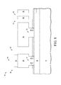
- MEMS device 10 Shown in FIG. 8 is MEMS device 10 after removing nitride portions 24, 26, and 28 and nitride layer 44. This exposes the top surface of metal layer 42 of contact stack 54. This leaves a completed MEMS device which can be subsequently packaged in conventional fashion and contacting metal layer 42. This removal may occur by using a dry plasma etch that is selective between nitride and polysilicon.
- FIG. 9 Shown in FIG. 9 , as an alternative to the embodiment of FIGS. 2-8 , is a MEMS device 70 that is MEMS device 10 of FIG. 1 after performing a patterned etch of layer 42 instead of depositing a layer of SiRN as shown in FIG. 2 . This leaves a portion of metal layer 42 in the opening in layer 40. In this example, there is a small space between the remaining portion of layer 42 and layer 40 so that a small portion of polysilicon layer 36 is exposed.
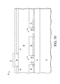
- MEMS device 70 Shown in FIG. 10 is MEMS device 70 after depositing a layer 54 of SiRN over the remaining portion of layer 42, the small portion of exposed polysilicon layer 36, and layer 40.
- MEMS device 70 Shown in FIG. 11 is MEMS device 70 after performing a patterned etch of layer 45 of SiRN which leaves SiRN on the sidewalls of the remaining portion of layer 42. This avoids the vapor phase HF etch from contacting any portion, even the sidewalls, of the remaining portion of layer 42.
- the covering the sidewalls is the primary difference from MEMS device 10 of FIG. 3 .
- MEMS device 70 of FIG. 11 is then processed as described for MEMS device 10 in FIGS. 4-8 .
- a protective layer preferably of SiRN, to protect the contact during the etch that removes the oxide that has the effect of giving the freedom of motion to the movable member made up of the polysilicon portions that remain as a continuous structural element.
- This etch that removes the oxide is very important in the predictable operation of the movable element.
- a vapor phase HF etch has been found to be very effective for this purpose. Due to the adverse effect of this etch on the contact, a sacrificial protective layer has been employed to be effective in avoiding the problem of contaminating the contact. Also the HF etch as been tuned so that the thickness of the sacrificial protective layer need not be excessive in achieving the desired etch stop over the contact.
- the method includes forming a sacrificial layer over a substrate.
- the method further includes forming a metal layer over the sacrificial layer.
- the method further includes forming a protection layer overlying the metal layer.
- the method further includes etching the protection layer and the metal layer to form a structure having a remaining portion of the protection layer formed over a remaining portion of the metal layer.
- the method further includes etching the sacrificial layer to form a movable portion of the MEMS device, wherein the remaining portion of the protection layer protects the remaining portion of the metal layer during the etching of the sacrificial layer to form the movable portion of the MEMS device.
- the method may have a further characterization by which a material used to form the protection layer and a thickness of the protection layer are selected such that after the step of the etching the sacrificial layer to form the movable portion of the MEMS device, a residual portion of the remaining portion of the protection layer remains over the remaining portion of the metal layer.
- the method may further comprise after etching the protection layer and the metal layer to form the structure, forming an insulating layer overlying the remaining portion of the protection layer.
- the method may have a further characterization by which the structure comprises a bond pad structure.
- the method may further comprise forming a conductive layer over the sacrificial layer and prior to etching the sacrificial layer to form the movable portion of the MEMS device, etching the conductive layer to form a feature of the movable portion.
- the method may have a further characterization by which the protection layer comprises one of a group consisting of silicon rich silicon nitride, titanium nitride, titanium and amorphous carbide.
- the method may have a further characterization by which the protection layer comprises silicon rich silicon nitride.
- the method includes forming a sacrificial layer over a substrate.
- the method further includes forming a metal layer over the sacrificial layer.
- the method further includes etching the metal layer to form a structure having a remaining portion of the metal layer.
- the method further includes forming a protection layer overlying at least the remaining portion of the metal layer.
- the method further includes etching the sacrificial layer to form a movable portion of the MEMS device, wherein the protection layer protects the remaining portion of the metal layer during the etching of the sacrificial layer to form the movable portion of the MEMS device.
- the method may have a further characterization by which a material used to form the protection layer and a thickness of the protection layer are selected such that after the step of the etching the sacrificial layer to form the movable portion of the MEMS device, a residual portion of the remaining portion of the sacrificial layer remains over the remaining portion of the metal layer.
- the method may further comprise prior to etching the protection layer, forming an insulating layer overlying the protection layer.
- the method may have a further characterization by which structure comprises a bond pad structure.
- the method may further comprise forming a conductive layer over the sacrificial layer and prior to etching the sacrificial layer to form the movable portion of the MEMS device, etching the conductive layer to form a feature of the movable portion.
- the method may have a further characterization by which the protection layer comprises one of a group consisting of silicon-rich silicon nitride, titanium nitride, titanium, and amorphous carbide.
- the method may have a further characterization by which the protection layer comprises silicon-rich silicon nitride.
- the method includes forming a sacrificial layer over a substrate.
- the method further includes forming a metal layer over the sacrificial layer.
- the method includes forming a protection layer overlying the metal layer.
- the method further includes etching the protection layer and the metal layer to form a bond pad structure having a remaining portion of the protection layer formed over a remaining portion of the metal layer.
- the method further includes forming an insulating layer overlying at least the remaining portion of the protection layer.
- the method further includes etching the sacrificial layer to form a movable portion of the MEMS device, wherein the remaining portion of the protection layer protects at least a top surface of the remaining portion of the metal layer, forming the bond pad structure, from contamination during the step of etching the sacrificial layer to form the movable portion of the MEMS device.
- the method may have a further characterization by which a material used to form the protection layer and a thickness of the protection layer are selected such that after the step of the etching the sacrificial layer to form the movable portion of the MEMS device, a residual portion of the remaining portion of the sacrificial layer remains over the remaining portion of the metal layer.
- the method may further comprise forming a conductive layer over the sacrificial layer and prior to etching the sacrificial layer to form the movable portion of the MEMS device, etching the conductive layer to form a feature of the movable portion.
- the method may have a further characterization by which the protection layer is selected from a group consisting of silicon nitride and titanium nitride.
- the method may have a further characterization by which the protection layer comprises silicon-rich nitride.
- the method may have a further characterization by which the protection layer comprises one of a group consisting of silicon-rich silicon nitride, titanium nitride, titanium, and amorphous carbide.
Landscapes
- Engineering & Computer Science (AREA)
- Microelectronics & Electronic Packaging (AREA)
- Manufacturing & Machinery (AREA)
- Computer Hardware Design (AREA)
- Physics & Mathematics (AREA)
- General Physics & Mathematics (AREA)
- Radar, Positioning & Navigation (AREA)
- Remote Sensing (AREA)
- Micromachines (AREA)
Abstract
Description
- This disclosure relates generally to MEMS devices, and more specifically, to methods of making MEMS devices.
- Micro-electro-mechanical-systems (MEMS) devices are finding more and more uses, especially for spatial sensing uses such accelerometers, position detectors, and gyroscopes. These functions are becoming more and more common and finding uses in many consumers devices such as mobile phones, automobiles, and electronic games. As the uses increase the demand for lower cost also increases which bears on having manufacturing processes that provide sufficient quality at high volume. One of the things that is typically involved with a MEMS device is a portion that has some freedom of movement, often in 3 axes. The manufacturing of this portion is critical to the functionality of the MEMS device. Integrating this key process with other features that must also be present presents difficulties.
- Accordingly, there is a need to improve upon processes for making a MEMS device particularly as it bears on providing a feature that has some level of freedom of motion.
- The present invention is illustrated by way of example and is not limited by the accompanying figures, in which like references indicate similar elements. Elements in the figures are illustrated for simplicity and clarity and have not necessarily been drawn to scale.
-
FIG. 1 is a cross section of a MEMS device at a stage in processing according to a first embodiment; -
FIG. 2 is a cross section of the MEMS device ofFIG. 1 at a subsequent stage in processing; -
FIG. 3 is a cross section of the MEMS device ofFIG. 2 at a subsequent stage in processing; -
FIG. 4 is a cross section of the MEMS device ofFIG. 3 at a subsequent stage in processing; -
FIG. 5 is a cross section of the MEMS device ofFIG. 4 at a subsequent stage in processing; -
FIG. 6 is a cross section of the MEMS device ofFIG. 5 at a subsequent stage in processing; -
FIG. 7 is a cross section of the MEMS device ofFIG. 6 at a subsequent stage in processing; -
FIG. 8 is a cross section of the MEMS device ofFIG. 7 at a subsequent stage in processing; -
FIG. 9 is a cross section of a MEMS device at a stage in processing according to a second embodiment; -
FIG. 10 is a cross section of the MEMS device ofFIG. 9 at a subsequent stage in processing; and -
FIG. 11 is a cross section of the MEMS device ofFIG. 10 at a subsequent stage in processing. - In one aspect, a micro-electro-mechanical-systems (MEMS) device is made using an etch that provides freedom of motion of a polysilicon member while protecting a contact pad from the etchants used to perform the etch that provides the freedom of motion. The protection is achieved by depositing a sacrificial layer and patterning it to leave a portion over the location of the contact pad. The etch tends to leave a layer on the contact pad, if it is unprotected, that makes it difficult to adhere a wire bond or other contacting material. The etch is very significant to the freedom of motion and thus is very important to control in order to achieve the needed performance of the MEMS device. The remaining portion of the sacrificial layer is removed after the etch to make the contact available for contacting. This is better understood by reference to the drawings and the following specification.
- The semiconductor substrate described herein can be any semiconductor material or combinations of materials, such as gallium arsenide, silicon germanium, silicon-on-insulator (SOI), silicon, monocrystalline silicon, the like, and combinations of the above.
- Shown in
FIG. 1 is aMEMS device 10 comprising asubstrate 12; athermal oxide layer 14 grown onsubstrate 14; a patterned polysilicon layer havingpolysilicon portions 16 18, and 22; a silicon nitride layer onpolysilicon portions thermal oxide layer 14 havingnitride portion 24 onpolysilicon portion 16 andthermal oxide layer 14,nitride portion 26 onpolysilicon portion 18, andnitride portion 28 onpolysilicon portion 22 andthermal oxide layer 14; a deposited oxide layer having anoxide portion 30 onnitride portion 24, anoxide portion 32 onnitride portion 26, and anoxide portion 34 onnitride portion 28; apolysilicon layer 36 overoxide portions thermal oxide layer 14; a deposited oxide layer overpolysilicon layer 36 having anoxide portion 38 and anoxide portion 40; and ametal layer 42 over depositedoxide layer 40 andpolysilicon layer 36. Aregion 31 ofpolysilicon layer 36 is betweenoxide portions nitride portions polysilicon portions region 33 ofpolysilicon layer 36 is betweenoxide portions nitride portions polysilicon portions region 35 of metal layer is betweenoxide portions thermal oxide 14; 0.35 micron forpolysilicon portions nitride portions oxide portions polysilicon layer 36; 0.4 micron foroxide portions metal layer 35. Other dimensions will work as well.Metal layer 42 may comprise aluminum and may include other materials as well such as copper and silicon.Oxide portions Polysilicon portion 18 should be conductive so if polyslicon is chosen for this purpose it should be doped. - Shown in
FIG. 2 isMEMS device 10 after depositing a silicon-rich silicon nitride (SiRN)layer 44 that may have a thickness of 0.75 micron. SiRNlayer 44 may have refractive index of 2.19. Other relative concentrations of silicon resulting in a lower or higher refractive index may also be effective. Stoichemetric silicon nitride has about a 2.02 refractive index. Thus it is desirable that the refractive index exceed 2.02. SiRN is preferable to stoichemetric silicon nitride because, for hydrofluoric acid (HF) in vapor form, silicon-rich silicon nitride etches more slowly. Although SiRN is the preferred material, other materials may also be effective forlayer 44. Exemplary materials are titanium nitride, titanium, and amorphous carbide. Other materials may also be effective. As noted by the examples,layer 44 may be a conductor or a dielectric. - Shown in
FIG. 3 isMEMS device 10 after performing a patterned etch ofmetal layer 42 andSiRN layer 44 aligned toregion 35 and thus leavingregion 35 ofmetal layer 42 and the portion of SiRNlayer 44 aligned toregion 31. - Shown in
FIG. 4 isMEMS device 10 after depositing alayer 46 of oxide having a thickness that may be 0.4 micron. - Shown in
FIG. 5 isMEMS device 10 afteretching openings oxide layer 46,oxide layer 40, andpolysilicon layer 36 to expose portions ofoxide portions Opening 48 surrounds acontact stack 54.Openings polysilicon layer 36 adjacent toopenings polysilicon layer 36. This will be the movable member of the MEMS device which may also be called the movable portion of the MEMS device. - Shown in
FIG. 6 is MEMS device after an oxide etch using vapor phase HF which removesoxide portions oxide layers Oxide portions layer 44 functions as an etch stop so thatmetal layer 42 does not receive the HF etch and is thus a protection layer as it protectsmetal layer 42.SiRN layer 44 is also etched but the vapor phase HF etch is tuned so that the oxide is etched much faster than SiRN. A consequence of this etch isresidue 58 onnitride portions residue 56 onSiRN layer 44. The removal ofoxide portions polysilicon layer 36 to be movable. Thus, the etch of oxide that has this effect in a MEMS device is sometimes called a release etch.Region 33 functions as a base for the movable member portion ofpolysilicon layer 36. Atregion 31 the portion ofpolysilicon layer 36 that is part ofcontact stack 54 makes contact topolysilicon portion 18 which in turn contacts the movable member atregion 33. The HF etch, if itcontacts metal layer 42, has been found to form a layer that is a compound comprising oxygen, aluminum, and fluorine. This compound makes it difficult to form a good electrical contact tometal layer 42. For example, gold does not adhere well to this compound. Further this compound is not easily removed.Residue 56 is also not good for forming electrical contact but residue is easily removed using techniques commonly used for cleaning after performing an etch. For example a rinse in hydrogen peroxide followed by a 350 degree Celsius bake is effective and which also is effective in removingresidue 58. Vapor phase HF processes may include tools wherein either an anhydrous HF liquid mixture is evaporated to form HF vapor or gaseous nitrogen is bubbled through a highly concentrated solution of HF and water. An effective process diluent is nitrogen gas. Gaseous isopropyl alcohol or similar hydrophobic compounds may be also added to the process in order to promote effective drying of the MEMS device. Processing chambers may operate at atmospheric pressure or at sub-atmospheric pressures. The temperature of the reaction may be held at room temperature or be performed at elevated temperatures (25-50 deg C). Further the process parameters are adjustable to achieve different rates for SiRN compared to deposited oxide. For example, the rate of oxide etching can be more than four times that of SiRN. This allows for flexibility in selecting the thickness of the SiRN layer. - Hydrogen fluoride (HF) is an effective method for etching silicon dioxide, a common sacrificial material used in MEMS processing. However, this etch in aqueous form may attack aluminum, particularly due to the presence of water. The use of vapor phase HF to etch oxide reduces the attack of aluminum during the etch. However, water vapor liberated by the etch of silicon dioxide can condense on the aluminum and result in the formation of undesirable compounds of aluminum, fluorine and oxygen.
- Shown in
FIG. 7 isMEMS device 10 after performing the rinse and bake to removeresidue 56 andresidue 58. - Shown in
FIG. 8 isMEMS device 10 after removingnitride portions nitride layer 44. This exposes the top surface ofmetal layer 42 ofcontact stack 54. This leaves a completed MEMS device which can be subsequently packaged in conventional fashion and contactingmetal layer 42. This removal may occur by using a dry plasma etch that is selective between nitride and polysilicon. - Shown in
FIG. 9 , as an alternative to the embodiment ofFIGS. 2-8 , is aMEMS device 70 that isMEMS device 10 ofFIG. 1 after performing a patterned etch oflayer 42 instead of depositing a layer of SiRN as shown inFIG. 2 . This leaves a portion ofmetal layer 42 in the opening inlayer 40. In this example, there is a small space between the remaining portion oflayer 42 andlayer 40 so that a small portion ofpolysilicon layer 36 is exposed. - Shown in
FIG. 10 isMEMS device 70 after depositing alayer 54 of SiRN over the remaining portion oflayer 42, the small portion of exposedpolysilicon layer 36, andlayer 40. - Shown in
FIG. 11 isMEMS device 70 after performing a patterned etch oflayer 45 of SiRN which leaves SiRN on the sidewalls of the remaining portion oflayer 42. This avoids the vapor phase HF etch from contacting any portion, even the sidewalls, of the remaining portion oflayer 42. The covering the sidewalls is the primary difference fromMEMS device 10 ofFIG. 3 . -
MEMS device 70 ofFIG. 11 is then processed as described forMEMS device 10 inFIGS. 4-8 . - Thus, it is seen that providing a protective layer, preferably of SiRN, to protect the contact during the etch that removes the oxide that has the effect of giving the freedom of motion to the movable member made up of the polysilicon portions that remain as a continuous structural element. This etch that removes the oxide is very important in the predictable operation of the movable element. A vapor phase HF etch has been found to be very effective for this purpose. Due to the adverse effect of this etch on the contact, a sacrificial protective layer has been employed to be effective in avoiding the problem of contaminating the contact. Also the HF etch as been tuned so that the thickness of the sacrificial protective layer need not be excessive in achieving the desired etch stop over the contact.
- By now it should be appreciated that there has been provided a method of forming a MEMS device. The method includes forming a sacrificial layer over a substrate. The method further includes forming a metal layer over the sacrificial layer. The method further includes forming a protection layer overlying the metal layer. The method further includes etching the protection layer and the metal layer to form a structure having a remaining portion of the protection layer formed over a remaining portion of the metal layer. The method further includes etching the sacrificial layer to form a movable portion of the MEMS device, wherein the remaining portion of the protection layer protects the remaining portion of the metal layer during the etching of the sacrificial layer to form the movable portion of the MEMS device. The method may have a further characterization by which a material used to form the protection layer and a thickness of the protection layer are selected such that after the step of the etching the sacrificial layer to form the movable portion of the MEMS device, a residual portion of the remaining portion of the protection layer remains over the remaining portion of the metal layer. The method may further comprise after etching the protection layer and the metal layer to form the structure, forming an insulating layer overlying the remaining portion of the protection layer. The method may have a further characterization by which the structure comprises a bond pad structure. The method may further comprise forming a conductive layer over the sacrificial layer and prior to etching the sacrificial layer to form the movable portion of the MEMS device, etching the conductive layer to form a feature of the movable portion. The method may have a further characterization by which the protection layer comprises one of a group consisting of silicon rich silicon nitride, titanium nitride, titanium and amorphous carbide. The method may have a further characterization by which the protection layer comprises silicon rich silicon nitride.
- Also described is a method of forming a MEMS device. The method includes forming a sacrificial layer over a substrate. The method further includes forming a metal layer over the sacrificial layer. The method further includes etching the metal layer to form a structure having a remaining portion of the metal layer. The method further includes forming a protection layer overlying at least the remaining portion of the metal layer. The method further includes etching the sacrificial layer to form a movable portion of the MEMS device, wherein the protection layer protects the remaining portion of the metal layer during the etching of the sacrificial layer to form the movable portion of the MEMS device. The method may have a further characterization by which a material used to form the protection layer and a thickness of the protection layer are selected such that after the step of the etching the sacrificial layer to form the movable portion of the MEMS device, a residual portion of the remaining portion of the sacrificial layer remains over the remaining portion of the metal layer. The method may further comprise prior to etching the protection layer, forming an insulating layer overlying the protection layer. The method may have a further characterization by which structure comprises a bond pad structure. The method may further comprise forming a conductive layer over the sacrificial layer and prior to etching the sacrificial layer to form the movable portion of the MEMS device, etching the conductive layer to form a feature of the movable portion. The method may have a further characterization by which the protection layer comprises one of a group consisting of silicon-rich silicon nitride, titanium nitride, titanium, and amorphous carbide. The method may have a further characterization by which the protection layer comprises silicon-rich silicon nitride.
- Described also is a method of forming a MEMS device. The method includes forming a sacrificial layer over a substrate. The method further includes forming a metal layer over the sacrificial layer. The method includes forming a protection layer overlying the metal layer. The method further includes etching the protection layer and the metal layer to form a bond pad structure having a remaining portion of the protection layer formed over a remaining portion of the metal layer. The method further includes forming an insulating layer overlying at least the remaining portion of the protection layer. The method further includes etching the sacrificial layer to form a movable portion of the MEMS device, wherein the remaining portion of the protection layer protects at least a top surface of the remaining portion of the metal layer, forming the bond pad structure, from contamination during the step of etching the sacrificial layer to form the movable portion of the MEMS device. The method may have a further characterization by which a material used to form the protection layer and a thickness of the protection layer are selected such that after the step of the etching the sacrificial layer to form the movable portion of the MEMS device, a residual portion of the remaining portion of the sacrificial layer remains over the remaining portion of the metal layer. The method may further comprise forming a conductive layer over the sacrificial layer and prior to etching the sacrificial layer to form the movable portion of the MEMS device, etching the conductive layer to form a feature of the movable portion. The method may have a further characterization by which the protection layer is selected from a group consisting of silicon nitride and titanium nitride. The method may have a further characterization by which the protection layer comprises silicon-rich nitride. The method may have a further characterization by which the protection layer comprises one of a group consisting of silicon-rich silicon nitride, titanium nitride, titanium, and amorphous carbide.
- Moreover, the terms "front," "back," "top," "bottom," "over," "under" and the like in the description and in the claims, if any, are used for descriptive purposes and not necessarily for describing permanent relative positions. It is understood that the terms so used are interchangeable under appropriate circumstances such that the embodiments of the invention described herein are, for example, capable of operation in other orientations than those illustrated or otherwise described herein.
- Although the invention is described herein with reference to specific embodiments, various modifications and changes can be made without departing from the scope of the present invention as set forth in the claims below. For example, another etch may be found to be effective as a release etch and still may result in deleterious effects on the contact and may benefit from using the sacrificial protective layer. Also described is that the polysilicon layer is patterned after the contact metal is patterned but the reverse may be the case in which
polysilicon layer 36 would be patterned for shaping the movable member and thenmetal layer 42 would be patterned to from the contact. Accordingly, the specification and figures are to be regarded in an illustrative rather than a restrictive sense, and all such modifications are intended to be included within the scope of the present invention. Any benefits, advantages, or solutions to problems that are described herein with regard to specific embodiments are not intended to be construed as a critical, required, or essential feature or element of any or all the claims. - Furthermore, the terms "a" or "an," as used herein, are defined as one or more than one. Also, the use of introductory phrases such as "at least one" and "one or more" in the claims should not be construed to imply that the introduction of another claim element by the indefinite articles "a" or "an" limits any particular claim containing such introduced claim element to inventions containing only one such element, even when the same claim includes the introductory phrases "one or more" or "at least one" and indefinite articles such as "a" or "an." The same holds true for the use of definite articles.
- Unless stated otherwise, terms such as "first" and "second" are used to arbitrarily distinguish between the elements such terms describe. Thus, these terms are not necessarily intended to indicate temporal or other prioritization of such elements.
Claims (15)
- A method of forming a MEMS device (10), the method comprising:forming a sacrificial layer (34) over a substrate (12);forming a metal layer (42) over the sacrificial layer (34);forming a protection layer (44) overlying the metal layer (42);etching the protection layer (44) and the metal layer (42) to form a structure (54) having
a remaining portion of the protection layer formed over a remaining portion of the metal layer; andetching the sacrificial layer (34) to form a movable portion of the MEMS device (10),wherein the remaining portion of the protection layer (44) protects the remaining portion of the metal layer (42) during the etching of the sacrificial layer (34) to form the movable portion of the MEMS device. - The method of claim 1, wherein a material used to form the protection layer (44) and a thickness of the protection layer (44) are selected such that after the step of the etching the sacrificial layer (34) to form the movable portion of the MEMS device (10), a residual portion (56) of the remaining portion of the protection layer (44) remains over the remaining portion of the metal layer (42).
- The method of claim 1 or 2 further comprising:after etching the protection layer (44) and the metal layer (42) to form the structure (54), forming an insulating layer (46) overlying the remaining portion of the protection layer (44).
- The method of claim 1, 2 or 3, wherein the structure (54) comprises a bond pad structure.
- The method of claim 1, 2, 3, or 4 further comprising:forming a conductive layer (36) over the sacrificial layer (34); andprior to etching the sacrificial layer to form the movable portion of the MEMS device (10), etching the conductive layer to form a feature of the movable portion.
- The method of claim 1,2, 3, 4, or 5, wherein the protection layer (44) comprises one of a group consisting of silicon-rich silicon nitride, titanium nitride, titanium, amorphous carbide.
- The method of claim 1,2, 3, 4, or 5, wherein the protection layer (44) comprises silicon-rich silicon nitride.
- A method of forming a MEMS device (10), the method comprising:forming a sacrificial layer (34) over a substrate (12);forming a metal layer (42) over the sacrificial layer (34);etching the metal layer (42) to form a structure having a remaining portion of the metal
layer (42);forming a protection layer (44) overlying at least the remaining portion of the metal layer (42); andetching the sacrificial layer (34) to form a movable portion of the MEMS device (10),wherein the protection layer (44) protects the remaining portion of the metal layer (42) during the etching of the sacrificial layer (34) to form the movable portion of the MEMS device. - The method of claim 8, wherein a material used to form the protection layer (44) and a thickness of the protection layer (44) are selected such that after the step of the etching the sacrificial layer (34) to form the movable portion of the MEMS device, a residual portion (56) of the sacrificial layer remains over the remaining portion of the metal layer.
- The method of claim 8 or 9 further comprising:prior to etching the protection layer (44), forming an insulating layer (46) overlying the protection layer.
- The method of claim 8, 9, or 10, wherein the structure comprises a bond pad structure.
- The method of claim 8, 9, 10, or 11 further comprising:forming a conductive layer (36) over the sacrificial layer (34); andprior to etching the sacrificial layer (34) to form the movable portion of the MEMS device (10), etching the conductive layer (36) to form a feature of the movable portion.
- The method of claim 8, 9, 10, 11 or 12, wherein the protection layer (44) comprises one of a group consisting of silicon-rich silicon nitride, titanium nitride, titanium, and amorphous carbide.
- The method of claim 8, 9, 10, 11 or 12, wherein the protection layer (44) comprises silicon-rich nitride.
- A MEMS device (10) obtainable with the method as claimed in any one of claims 1-14.
Applications Claiming Priority (1)
| Application Number | Priority Date | Filing Date | Title |
|---|---|---|---|
| US12/916,395 US8455286B2 (en) | 2010-10-29 | 2010-10-29 | Method of making a micro-electro-mechanical-systems (MEMS) device |
Publications (3)
| Publication Number | Publication Date |
|---|---|
| EP2476644A2 true EP2476644A2 (en) | 2012-07-18 |
| EP2476644A3 EP2476644A3 (en) | 2014-01-22 |
| EP2476644B1 EP2476644B1 (en) | 2018-12-12 |
Family
ID=44772934
Family Applications (1)
| Application Number | Title | Priority Date | Filing Date |
|---|---|---|---|
| EP11184861.0A Active EP2476644B1 (en) | 2010-10-29 | 2011-10-12 | Method of making a MEMS device |
Country Status (5)
| Country | Link |
|---|---|
| US (1) | US8455286B2 (en) |
| EP (1) | EP2476644B1 (en) |
| JP (1) | JP6016290B2 (en) |
| KR (1) | KR20120047818A (en) |
| CN (1) | CN102452638A (en) |
Cited By (1)
| Publication number | Priority date | Publication date | Assignee | Title |
|---|---|---|---|---|
| CN104671190A (en) * | 2013-11-27 | 2015-06-03 | 中芯国际集成电路制造(上海)有限公司 | Protecting method for device surface |
Families Citing this family (10)
| Publication number | Priority date | Publication date | Assignee | Title |
|---|---|---|---|---|
| TWI454868B (en) * | 2012-11-02 | 2014-10-01 | Ind Tech Res Inst | Target-oriented numerical control automatic tuning system and method |
| JP6381332B2 (en) * | 2013-09-19 | 2018-08-29 | 浜松ホトニクス株式会社 | Manufacturing method of semiconductor device |
| DE102014202820A1 (en) * | 2014-02-17 | 2015-08-20 | Robert Bosch Gmbh | Layer arrangement for a micromechanical component |
| US9663356B2 (en) * | 2014-06-18 | 2017-05-30 | Nxp Usa, Inc. | Etch release residue removal using anhydrous solution |
| CN105565252B (en) * | 2014-10-10 | 2018-03-30 | 中芯国际集成电路制造(上海)有限公司 | A kind of MEMS and preparation method thereof, electronic installation |
| CN105293419B (en) * | 2015-10-15 | 2016-12-07 | 华东光电集成器件研究所 | A MEMS device for preventing etching damage of suspension layer |
| JP6572143B2 (en) * | 2016-01-27 | 2019-09-04 | Koa株式会社 | Chip resistor and manufacturing method thereof |
| CN108408683B (en) * | 2017-02-09 | 2020-08-18 | 中芯国际集成电路制造(上海)有限公司 | Method for manufacturing semiconductor device |
| GB2606747B (en) * | 2021-05-19 | 2024-11-20 | Memsstar Ltd | Method of manufacturing a microstructure |
| DE102022200343B3 (en) | 2022-01-13 | 2023-02-16 | Robert Bosch Gesellschaft mit beschränkter Haftung | Method for producing a bond pad for a micromechanical sensor element |
Family Cites Families (18)
| Publication number | Priority date | Publication date | Assignee | Title |
|---|---|---|---|---|
| JP3603347B2 (en) * | 1994-10-12 | 2004-12-22 | 株式会社デンソー | Manufacturing method of semiconductor sensor |
| US5698112A (en) * | 1994-11-24 | 1997-12-16 | Siemens Aktiengesellschaft | Corrosion protection for micromechanical metal layers |
| US6006764A (en) | 1997-01-28 | 1999-12-28 | Taiwan Semiconductor Manufacturing Company, Ltd. | Method of stripping photoresist from Al bonding pads that prevents corrosion |
| US5930664A (en) | 1997-07-24 | 1999-07-27 | Taiwan Semiconductor Manufacturing Company, Ltd. | Process for preventing corrosion of aluminum bonding pads after passivation/ARC layer etching |
| JP4214565B2 (en) * | 1998-07-22 | 2009-01-28 | 株式会社デンソー | Manufacturing method of semiconductor dynamic quantity sensor |
| US6221752B1 (en) | 1998-08-20 | 2001-04-24 | United Microelectronics Corp. | Method of mending erosion of bonding pad |
| US6440766B1 (en) * | 2000-02-16 | 2002-08-27 | Analog Devices Imi, Inc. | Microfabrication using germanium-based release masks |
| JP2002103299A (en) * | 2000-09-22 | 2002-04-09 | Aisin Seiki Co Ltd | Manufacturing method of micromachine |
| DE10226028A1 (en) * | 2002-06-12 | 2003-12-24 | Bosch Gmbh Robert | Component and method for its production |
| US7405860B2 (en) * | 2002-11-26 | 2008-07-29 | Texas Instruments Incorporated | Spatial light modulators with light blocking/absorbing areas |
| US7041611B2 (en) * | 2004-03-17 | 2006-05-09 | Wisconsin Alumni Research Foundation | Enhancement of fabrication yields of nanomechanical devices by thin film deposition |
| US7172978B2 (en) * | 2004-07-21 | 2007-02-06 | Hewlett-Packard Development Company, L.P. | MEMS device polymer film deposition process |
| US20070090474A1 (en) * | 2005-09-08 | 2007-04-26 | Li Gary G | MEMS device and method of fabrication |
| US7682860B2 (en) | 2006-03-21 | 2010-03-23 | Dalsa Semiconductor Inc. | Protection capsule for MEMS devices |
| JP4849614B2 (en) * | 2006-11-01 | 2012-01-11 | 東京エレクトロン株式会社 | Substrate processing method and substrate processing system |
| US7585754B2 (en) | 2008-01-10 | 2009-09-08 | Winbond Electronics Corp. | Method of forming bonding pad opening |
| US20100065930A1 (en) * | 2008-09-18 | 2010-03-18 | Rohm Co., Ltd. | Method of etching sacrificial layer, method of manufacturing MEMS device, MEMS device and MEMS sensor |
| US8101469B2 (en) * | 2009-07-02 | 2012-01-24 | Advanced Microfab, LLC | Method of forming monolithic CMOS-MEMS hybrid integrated, packaged structures |
-
2010
- 2010-10-29 US US12/916,395 patent/US8455286B2/en active Active
-
2011
- 2011-09-30 JP JP2011216769A patent/JP6016290B2/en not_active Expired - Fee Related
- 2011-10-12 EP EP11184861.0A patent/EP2476644B1/en active Active
- 2011-10-24 CN CN2011103347829A patent/CN102452638A/en active Pending
- 2011-10-28 KR KR1020110111454A patent/KR20120047818A/en not_active Withdrawn
Non-Patent Citations (1)
| Title |
|---|
| None |
Cited By (2)
| Publication number | Priority date | Publication date | Assignee | Title |
|---|---|---|---|---|
| CN104671190A (en) * | 2013-11-27 | 2015-06-03 | 中芯国际集成电路制造(上海)有限公司 | Protecting method for device surface |
| CN104671190B (en) * | 2013-11-27 | 2017-07-14 | 中芯国际集成电路制造(上海)有限公司 | The guard method of device surface |
Also Published As
| Publication number | Publication date |
|---|---|
| CN102452638A (en) | 2012-05-16 |
| JP2012096350A (en) | 2012-05-24 |
| EP2476644B1 (en) | 2018-12-12 |
| EP2476644A3 (en) | 2014-01-22 |
| JP6016290B2 (en) | 2016-10-26 |
| US20120107993A1 (en) | 2012-05-03 |
| US8455286B2 (en) | 2013-06-04 |
| KR20120047818A (en) | 2012-05-14 |
Similar Documents
| Publication | Publication Date | Title |
|---|---|---|
| US8455286B2 (en) | Method of making a micro-electro-mechanical-systems (MEMS) device | |
| US8791021B2 (en) | Silicon germanium mask for deep silicon etching | |
| US7052623B1 (en) | Method for processing silicon using etching processes | |
| CN105374670B (en) | Semiconductor structure with coplanar recessed gate layer and method of making the same | |
| US8221642B2 (en) | Methods for removing dielectric materials | |
| US8253243B2 (en) | Bonded wafer substrate utilizing roughened surfaces for use in MEMS structures | |
| US7998775B2 (en) | Silicon undercut prevention in sacrificial oxide release process and resulting MEMS structures | |
| JP4671729B2 (en) | Semiconductor device and manufacturing method thereof | |
| US9290378B2 (en) | MEMS capping method | |
| KR100450679B1 (en) | Manufacturing method for storage node of semiconductor memory device using two step etching process | |
| EP3316281A1 (en) | Method of structuring a semiconductor device without pattern collapse | |
| EP2682363A1 (en) | Method for producing a mems device including a vapour release step | |
| CN113437044B (en) | Microstructure and patterning method thereof and micro-electromechanical system device | |
| CN105084299A (en) | Forming method of semiconductor structure | |
| US9663356B2 (en) | Etch release residue removal using anhydrous solution | |
| US8143158B2 (en) | Method and device of preventing delamination of semiconductor layers | |
| EP1482539A1 (en) | Preparation method for protecting the back side of a wafer and back side protected wafer | |
| US20150087134A1 (en) | Semiconductor isolation region uniformity | |
| WO2001057921A1 (en) | Etching solution and method | |
| TWI921757B (en) | Etching methods using silicon-containing hydrofluorocarbons | |
| TWI914748B (en) | Etching methods using silicon-containing hydrofluorocarbons | |
| TWI914747B (en) | Etching methods using silicon-containing hydrofluorocarbons | |
| Sh'f | Serry et al.(43) Pub. Date: Sep. 6, 2012 | |
| JP2007109718A (en) | Manufacturing method of semiconductor device | |
| Serry et al. | Silicon germanium mask for deep silicon etching |
Legal Events
| Date | Code | Title | Description |
|---|---|---|---|
| PUAI | Public reference made under article 153(3) epc to a published international application that has entered the european phase |
Free format text: ORIGINAL CODE: 0009012 |
|
| AK | Designated contracting states |
Kind code of ref document: A2 Designated state(s): AL AT BE BG CH CY CZ DE DK EE ES FI FR GB GR HR HU IE IS IT LI LT LU LV MC MK MT NL NO PL PT RO RS SE SI SK SM TR |
|
| AX | Request for extension of the european patent |
Extension state: BA ME |
|
| PUAL | Search report despatched |
Free format text: ORIGINAL CODE: 0009013 |
|
| AK | Designated contracting states |
Kind code of ref document: A3 Designated state(s): AL AT BE BG CH CY CZ DE DK EE ES FI FR GB GR HR HU IE IS IT LI LT LU LV MC MK MT NL NO PL PT RO RS SE SI SK SM TR |
|
| AX | Request for extension of the european patent |
Extension state: BA ME |
|
| RIC1 | Information provided on ipc code assigned before grant |
Ipc: B81C 1/00 20060101AFI20131217BHEP |
|
| 17P | Request for examination filed |
Effective date: 20140722 |
|
| RBV | Designated contracting states (corrected) |
Designated state(s): AL AT BE BG CH CY CZ DE DK EE ES FI FR GB GR HR HU IE IS IT LI LT LU LV MC MK MT NL NO PL PT RO RS SE SI SK SM TR |
|
| RAP1 | Party data changed (applicant data changed or rights of an application transferred) |
Owner name: NXP USA, INC. |
|
| STAA | Information on the status of an ep patent application or granted ep patent |
Free format text: STATUS: EXAMINATION IS IN PROGRESS |
|
| 17Q | First examination report despatched |
Effective date: 20170619 |
|
| GRAP | Despatch of communication of intention to grant a patent |
Free format text: ORIGINAL CODE: EPIDOSNIGR1 |
|
| STAA | Information on the status of an ep patent application or granted ep patent |
Free format text: STATUS: GRANT OF PATENT IS INTENDED |
|
| INTG | Intention to grant announced |
Effective date: 20180626 |
|
| GRAJ | Information related to disapproval of communication of intention to grant by the applicant or resumption of examination proceedings by the epo deleted |
Free format text: ORIGINAL CODE: EPIDOSDIGR1 |
|
| STAA | Information on the status of an ep patent application or granted ep patent |
Free format text: STATUS: EXAMINATION IS IN PROGRESS |
|
| INTC | Intention to grant announced (deleted) | ||
| GRAP | Despatch of communication of intention to grant a patent |
Free format text: ORIGINAL CODE: EPIDOSNIGR1 |
|
| STAA | Information on the status of an ep patent application or granted ep patent |
Free format text: STATUS: GRANT OF PATENT IS INTENDED |
|
| GRAS | Grant fee paid |
Free format text: ORIGINAL CODE: EPIDOSNIGR3 |
|
| INTG | Intention to grant announced |
Effective date: 20180925 |
|
| GRAA | (expected) grant |
Free format text: ORIGINAL CODE: 0009210 |
|
| STAA | Information on the status of an ep patent application or granted ep patent |
Free format text: STATUS: THE PATENT HAS BEEN GRANTED |
|
| AK | Designated contracting states |
Kind code of ref document: B1 Designated state(s): AL AT BE BG CH CY CZ DE DK EE ES FI FR GB GR HR HU IE IS IT LI LT LU LV MC MK MT NL NO PL PT RO RS SE SI SK SM TR |
|
| REG | Reference to a national code |
Ref country code: GB Ref legal event code: FG4D |
|
| REG | Reference to a national code |
Ref country code: CH Ref legal event code: EP |
|
| REG | Reference to a national code |
Ref country code: AT Ref legal event code: REF Ref document number: 1075729 Country of ref document: AT Kind code of ref document: T Effective date: 20181215 |
|
| REG | Reference to a national code |
Ref country code: DE Ref legal event code: R096 Ref document number: 602011054710 Country of ref document: DE |
|
| REG | Reference to a national code |
Ref country code: IE Ref legal event code: FG4D |
|
| REG | Reference to a national code |
Ref country code: NL Ref legal event code: MP Effective date: 20181212 |
|
| REG | Reference to a national code |
Ref country code: LT Ref legal event code: MG4D |
|
| PG25 | Lapsed in a contracting state [announced via postgrant information from national office to epo] |
Ref country code: ES Free format text: LAPSE BECAUSE OF FAILURE TO SUBMIT A TRANSLATION OF THE DESCRIPTION OR TO PAY THE FEE WITHIN THE PRESCRIBED TIME-LIMIT Effective date: 20181212 Ref country code: LV Free format text: LAPSE BECAUSE OF FAILURE TO SUBMIT A TRANSLATION OF THE DESCRIPTION OR TO PAY THE FEE WITHIN THE PRESCRIBED TIME-LIMIT Effective date: 20181212 Ref country code: FI Free format text: LAPSE BECAUSE OF FAILURE TO SUBMIT A TRANSLATION OF THE DESCRIPTION OR TO PAY THE FEE WITHIN THE PRESCRIBED TIME-LIMIT Effective date: 20181212 Ref country code: BG Free format text: LAPSE BECAUSE OF FAILURE TO SUBMIT A TRANSLATION OF THE DESCRIPTION OR TO PAY THE FEE WITHIN THE PRESCRIBED TIME-LIMIT Effective date: 20190312 Ref country code: HR Free format text: LAPSE BECAUSE OF FAILURE TO SUBMIT A TRANSLATION OF THE DESCRIPTION OR TO PAY THE FEE WITHIN THE PRESCRIBED TIME-LIMIT Effective date: 20181212 Ref country code: NO Free format text: LAPSE BECAUSE OF FAILURE TO SUBMIT A TRANSLATION OF THE DESCRIPTION OR TO PAY THE FEE WITHIN THE PRESCRIBED TIME-LIMIT Effective date: 20190312 Ref country code: LT Free format text: LAPSE BECAUSE OF FAILURE TO SUBMIT A TRANSLATION OF THE DESCRIPTION OR TO PAY THE FEE WITHIN THE PRESCRIBED TIME-LIMIT Effective date: 20181212 |
|
| REG | Reference to a national code |
Ref country code: AT Ref legal event code: MK05 Ref document number: 1075729 Country of ref document: AT Kind code of ref document: T Effective date: 20181212 |
|
| PG25 | Lapsed in a contracting state [announced via postgrant information from national office to epo] |
Ref country code: RS Free format text: LAPSE BECAUSE OF FAILURE TO SUBMIT A TRANSLATION OF THE DESCRIPTION OR TO PAY THE FEE WITHIN THE PRESCRIBED TIME-LIMIT Effective date: 20181212 Ref country code: GR Free format text: LAPSE BECAUSE OF FAILURE TO SUBMIT A TRANSLATION OF THE DESCRIPTION OR TO PAY THE FEE WITHIN THE PRESCRIBED TIME-LIMIT Effective date: 20190313 Ref country code: SE Free format text: LAPSE BECAUSE OF FAILURE TO SUBMIT A TRANSLATION OF THE DESCRIPTION OR TO PAY THE FEE WITHIN THE PRESCRIBED TIME-LIMIT Effective date: 20181212 Ref country code: AL Free format text: LAPSE BECAUSE OF FAILURE TO SUBMIT A TRANSLATION OF THE DESCRIPTION OR TO PAY THE FEE WITHIN THE PRESCRIBED TIME-LIMIT Effective date: 20181212 |
|
| PG25 | Lapsed in a contracting state [announced via postgrant information from national office to epo] |
Ref country code: NL Free format text: LAPSE BECAUSE OF FAILURE TO SUBMIT A TRANSLATION OF THE DESCRIPTION OR TO PAY THE FEE WITHIN THE PRESCRIBED TIME-LIMIT Effective date: 20181212 |
|
| PG25 | Lapsed in a contracting state [announced via postgrant information from national office to epo] |
Ref country code: PL Free format text: LAPSE BECAUSE OF FAILURE TO SUBMIT A TRANSLATION OF THE DESCRIPTION OR TO PAY THE FEE WITHIN THE PRESCRIBED TIME-LIMIT Effective date: 20181212 Ref country code: PT Free format text: LAPSE BECAUSE OF FAILURE TO SUBMIT A TRANSLATION OF THE DESCRIPTION OR TO PAY THE FEE WITHIN THE PRESCRIBED TIME-LIMIT Effective date: 20190412 Ref country code: CZ Free format text: LAPSE BECAUSE OF FAILURE TO SUBMIT A TRANSLATION OF THE DESCRIPTION OR TO PAY THE FEE WITHIN THE PRESCRIBED TIME-LIMIT Effective date: 20181212 Ref country code: IT Free format text: LAPSE BECAUSE OF FAILURE TO SUBMIT A TRANSLATION OF THE DESCRIPTION OR TO PAY THE FEE WITHIN THE PRESCRIBED TIME-LIMIT Effective date: 20181212 |
|
| PG25 | Lapsed in a contracting state [announced via postgrant information from national office to epo] |
Ref country code: RO Free format text: LAPSE BECAUSE OF FAILURE TO SUBMIT A TRANSLATION OF THE DESCRIPTION OR TO PAY THE FEE WITHIN THE PRESCRIBED TIME-LIMIT Effective date: 20181212 Ref country code: IS Free format text: LAPSE BECAUSE OF FAILURE TO SUBMIT A TRANSLATION OF THE DESCRIPTION OR TO PAY THE FEE WITHIN THE PRESCRIBED TIME-LIMIT Effective date: 20190412 Ref country code: SK Free format text: LAPSE BECAUSE OF FAILURE TO SUBMIT A TRANSLATION OF THE DESCRIPTION OR TO PAY THE FEE WITHIN THE PRESCRIBED TIME-LIMIT Effective date: 20181212 Ref country code: EE Free format text: LAPSE BECAUSE OF FAILURE TO SUBMIT A TRANSLATION OF THE DESCRIPTION OR TO PAY THE FEE WITHIN THE PRESCRIBED TIME-LIMIT Effective date: 20181212 Ref country code: SM Free format text: LAPSE BECAUSE OF FAILURE TO SUBMIT A TRANSLATION OF THE DESCRIPTION OR TO PAY THE FEE WITHIN THE PRESCRIBED TIME-LIMIT Effective date: 20181212 |
|
| REG | Reference to a national code |
Ref country code: DE Ref legal event code: R097 Ref document number: 602011054710 Country of ref document: DE |
|
| PLBE | No opposition filed within time limit |
Free format text: ORIGINAL CODE: 0009261 |
|
| STAA | Information on the status of an ep patent application or granted ep patent |
Free format text: STATUS: NO OPPOSITION FILED WITHIN TIME LIMIT |
|
| PG25 | Lapsed in a contracting state [announced via postgrant information from national office to epo] |
Ref country code: SI Free format text: LAPSE BECAUSE OF FAILURE TO SUBMIT A TRANSLATION OF THE DESCRIPTION OR TO PAY THE FEE WITHIN THE PRESCRIBED TIME-LIMIT Effective date: 20181212 Ref country code: DK Free format text: LAPSE BECAUSE OF FAILURE TO SUBMIT A TRANSLATION OF THE DESCRIPTION OR TO PAY THE FEE WITHIN THE PRESCRIBED TIME-LIMIT Effective date: 20181212 Ref country code: AT Free format text: LAPSE BECAUSE OF FAILURE TO SUBMIT A TRANSLATION OF THE DESCRIPTION OR TO PAY THE FEE WITHIN THE PRESCRIBED TIME-LIMIT Effective date: 20181212 |
|
| 26N | No opposition filed |
Effective date: 20190913 |
|
| PG25 | Lapsed in a contracting state [announced via postgrant information from national office to epo] |
Ref country code: TR Free format text: LAPSE BECAUSE OF FAILURE TO SUBMIT A TRANSLATION OF THE DESCRIPTION OR TO PAY THE FEE WITHIN THE PRESCRIBED TIME-LIMIT Effective date: 20181212 |
|
| PG25 | Lapsed in a contracting state [announced via postgrant information from national office to epo] |
Ref country code: MC Free format text: LAPSE BECAUSE OF FAILURE TO SUBMIT A TRANSLATION OF THE DESCRIPTION OR TO PAY THE FEE WITHIN THE PRESCRIBED TIME-LIMIT Effective date: 20181212 |
|
| REG | Reference to a national code |
Ref country code: CH Ref legal event code: PL |
|
| PG25 | Lapsed in a contracting state [announced via postgrant information from national office to epo] |
Ref country code: LI Free format text: LAPSE BECAUSE OF NON-PAYMENT OF DUE FEES Effective date: 20191031 Ref country code: CH Free format text: LAPSE BECAUSE OF NON-PAYMENT OF DUE FEES Effective date: 20191031 Ref country code: LU Free format text: LAPSE BECAUSE OF NON-PAYMENT OF DUE FEES Effective date: 20191012 |
|
| REG | Reference to a national code |
Ref country code: BE Ref legal event code: MM Effective date: 20191031 |
|
| PG25 | Lapsed in a contracting state [announced via postgrant information from national office to epo] |
Ref country code: BE Free format text: LAPSE BECAUSE OF NON-PAYMENT OF DUE FEES Effective date: 20191031 |
|
| PG25 | Lapsed in a contracting state [announced via postgrant information from national office to epo] |
Ref country code: IE Free format text: LAPSE BECAUSE OF NON-PAYMENT OF DUE FEES Effective date: 20191012 |
|
| PG25 | Lapsed in a contracting state [announced via postgrant information from national office to epo] |
Ref country code: CY Free format text: LAPSE BECAUSE OF FAILURE TO SUBMIT A TRANSLATION OF THE DESCRIPTION OR TO PAY THE FEE WITHIN THE PRESCRIBED TIME-LIMIT Effective date: 20181212 |
|
| PG25 | Lapsed in a contracting state [announced via postgrant information from national office to epo] |
Ref country code: HU Free format text: LAPSE BECAUSE OF FAILURE TO SUBMIT A TRANSLATION OF THE DESCRIPTION OR TO PAY THE FEE WITHIN THE PRESCRIBED TIME-LIMIT; INVALID AB INITIO Effective date: 20111012 Ref country code: MT Free format text: LAPSE BECAUSE OF FAILURE TO SUBMIT A TRANSLATION OF THE DESCRIPTION OR TO PAY THE FEE WITHIN THE PRESCRIBED TIME-LIMIT Effective date: 20181212 |
|
| PG25 | Lapsed in a contracting state [announced via postgrant information from national office to epo] |
Ref country code: MK Free format text: LAPSE BECAUSE OF FAILURE TO SUBMIT A TRANSLATION OF THE DESCRIPTION OR TO PAY THE FEE WITHIN THE PRESCRIBED TIME-LIMIT Effective date: 20181212 |
|
| P01 | Opt-out of the competence of the unified patent court (upc) registered |
Effective date: 20230725 |
|
| PGFP | Annual fee paid to national office [announced via postgrant information from national office to epo] |
Ref country code: GB Payment date: 20230920 Year of fee payment: 13 |
|
| PGFP | Annual fee paid to national office [announced via postgrant information from national office to epo] |
Ref country code: FR Payment date: 20230920 Year of fee payment: 13 |
|
| GBPC | Gb: european patent ceased through non-payment of renewal fee |
Effective date: 20241012 |
|
| PG25 | Lapsed in a contracting state [announced via postgrant information from national office to epo] |
Ref country code: GB Free format text: LAPSE BECAUSE OF NON-PAYMENT OF DUE FEES Effective date: 20241012 |
|
| PG25 | Lapsed in a contracting state [announced via postgrant information from national office to epo] |
Ref country code: FR Free format text: LAPSE BECAUSE OF NON-PAYMENT OF DUE FEES Effective date: 20241031 |
|
| PGFP | Annual fee paid to national office [announced via postgrant information from national office to epo] |
Ref country code: DE Payment date: 20250923 Year of fee payment: 15 |