EP2475102A1 - Switched capacitor circuit and ad conversion circuit - Google Patents
Switched capacitor circuit and ad conversion circuit Download PDFInfo
- Publication number
- EP2475102A1 EP2475102A1 EP09848996A EP09848996A EP2475102A1 EP 2475102 A1 EP2475102 A1 EP 2475102A1 EP 09848996 A EP09848996 A EP 09848996A EP 09848996 A EP09848996 A EP 09848996A EP 2475102 A1 EP2475102 A1 EP 2475102A1
- Authority
- EP
- European Patent Office
- Prior art keywords
- circuit
- capacitor
- mdac
- operation mode
- sampling
- Prior art date
- Legal status (The legal status is an assumption and is not a legal conclusion. Google has not performed a legal analysis and makes no representation as to the accuracy of the status listed.)
- Withdrawn
Links
Images


















Classifications
-
- H—ELECTRICITY
- H03—ELECTRONIC CIRCUITRY
- H03M—CODING; DECODING; CODE CONVERSION IN GENERAL
- H03M1/00—Analogue/digital conversion; Digital/analogue conversion
- H03M1/12—Analogue/digital converters
-
- H—ELECTRICITY
- H03—ELECTRONIC CIRCUITRY
- H03M—CODING; DECODING; CODE CONVERSION IN GENERAL
- H03M1/00—Analogue/digital conversion; Digital/analogue conversion
- H03M1/06—Continuously compensating for, or preventing, undesired influence of physical parameters
-
- H—ELECTRICITY
- H03—ELECTRONIC CIRCUITRY
- H03K—PULSE TECHNIQUE
- H03K5/00—Manipulating of pulses not covered by one of the other main groups of this subclass
- H03K5/01—Shaping pulses
- H03K5/08—Shaping pulses by limiting; by thresholding; by slicing, i.e. combined limiting and thresholding
-
- H—ELECTRICITY
- H03—ELECTRONIC CIRCUITRY
- H03M—CODING; DECODING; CODE CONVERSION IN GENERAL
- H03M1/00—Analogue/digital conversion; Digital/analogue conversion
- H03M1/12—Analogue/digital converters
- H03M1/34—Analogue value compared with reference values
- H03M1/38—Analogue value compared with reference values sequentially only, e.g. successive approximation type
- H03M1/44—Sequential comparisons in series-connected stages with change in value of analogue signal
-
- H—ELECTRICITY
- H03—ELECTRONIC CIRCUITRY
- H03M—CODING; DECODING; CODE CONVERSION IN GENERAL
- H03M1/00—Analogue/digital conversion; Digital/analogue conversion
- H03M1/66—Digital/analogue converters
-
- H—ELECTRICITY
- H03—ELECTRONIC CIRCUITRY
- H03M—CODING; DECODING; CODE CONVERSION IN GENERAL
- H03M1/00—Analogue/digital conversion; Digital/analogue conversion
- H03M1/12—Analogue/digital converters
- H03M1/14—Conversion in steps with each step involving the same or a different conversion means and delivering more than one bit
- H03M1/16—Conversion in steps with each step involving the same or a different conversion means and delivering more than one bit with scale factor modification, i.e. by changing the amplification between the steps
- H03M1/162—Conversion in steps with each step involving the same or a different conversion means and delivering more than one bit with scale factor modification, i.e. by changing the amplification between the steps the steps being performed sequentially in a single stage, i.e. recirculation type
-
- H—ELECTRICITY
- H03—ELECTRONIC CIRCUITRY
- H03M—CODING; DECODING; CODE CONVERSION IN GENERAL
- H03M1/00—Analogue/digital conversion; Digital/analogue conversion
- H03M1/12—Analogue/digital converters
- H03M1/14—Conversion in steps with each step involving the same or a different conversion means and delivering more than one bit
- H03M1/16—Conversion in steps with each step involving the same or a different conversion means and delivering more than one bit with scale factor modification, i.e. by changing the amplification between the steps
- H03M1/164—Conversion in steps with each step involving the same or a different conversion means and delivering more than one bit with scale factor modification, i.e. by changing the amplification between the steps the steps being performed sequentially in series-connected stages
- H03M1/167—Conversion in steps with each step involving the same or a different conversion means and delivering more than one bit with scale factor modification, i.e. by changing the amplification between the steps the steps being performed sequentially in series-connected stages all stages comprising simultaneous converters
- H03M1/168—Conversion in steps with each step involving the same or a different conversion means and delivering more than one bit with scale factor modification, i.e. by changing the amplification between the steps the steps being performed sequentially in series-connected stages all stages comprising simultaneous converters and delivering the same number of bits
Definitions
- the embodiments discussed herein are related to a switched capacitor circuit and an AD conversion circuit.
- Switched capacitor circuits are widely used in high-resolution, low-power AD (Analog-to-Digital) converters, DA (Digital-to-Analog) converters, filters, etc.
- AD Analog-to-Digital
- DA Digital-to-Analog
- a switched capacitor circuit includes a capacitor, a switch, and an amplifier, and this type of circuit is applied, for example, to an MDAC (Multiplying DAC) or the like used as a basic building block in a pipelined AD conversion circuit or a cyclic AD conversion circuit.
- MDAC Multiplying DAC
- an AD conversion circuit and a switched capacitor circuit (MDAC) to be used therein will be described as examples, but as stated above, the switched capacitor circuit is also applicable to a DA converter, a filter, etc.
- MDAC switched capacitor circuit
- the switched capacitor circuit is applied, for example, to an MDAC or the like in a pipelined AD conversion circuit.
- a switched capacitor circuit included in a circuit including a load circuit, configured to be operable in two or more kinds of operation modes including a first operation mode and a second operation mode.
- the switched capacitor circuit includes two or more internal capacitors, one or more amplifiers, and two or more internal switches.
- the load circuit includes a sampling capacitor, provided at a stage subsequent to the switched capacitor circuit, and a sampling switch for controlling connection/disconnection of the sampling capacitor.
- the sampling switch at the subsequent stage is turned off, thereby decoupling an output voltage of the switched capacitor circuit from the sampling capacitor at the subsequent stage, and the switched capacitor circuit performs computation.
- the sampling switch at the subsequent stage is turned on, thereby sampling the output voltage of the switched capacitor circuit onto the sampling capacitor.
- the switched capacitor circuit performs control to disconnect one or more of the internal capacitors by the internal switches.
- the switched capacitor circuit and AD conversion circuit disclosed herein offers the effect of being able to enhance the speed of computation, reduce the power consumption of the amplifier, or reduce the footprint of the circuit, and so on.
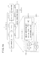
- FIG. 1A is a block diagram illustrating one example of an AD conversion circuit
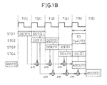
- FIG. 1B and FIG. 1C are diagrams for explaining the operation of the AD conversion circuit of FIG. 1A .
- the AD conversion circuit hereinafter described with reference to FIG. 1A , FIG. 1B , and FIG. 1C is a pipelined AD conversion circuit.
- the circuit that becomes important in achieving higher speed, lower power consumption, and smaller area is the MDAC (Multiplying DAC: switched capacitor circuit) that is used as the basic building block of the cell array.
- MDAC Multiplying DAC: switched capacitor circuit
- the pipelined AD conversion circuit 1 includes a sample-and-hold (S/H) circuit 11, a number, N-1, of stage circuits (STG-1 to STG-(N-1)) 10-1 to 10-(N-1), a flash AD converter (flash ADC) 12 at the last stage, and a digital correction circuit (code conversion circuit) 13.
- S/H sample-and-hold
- N-1 number, of stage circuits (STG-1 to STG-(N-1)) 10-1 to 10-(N-1)
- flash AD converter flash ADC
- code conversion circuit code conversion circuit
- the sample-and-hold circuit 11 samples an input voltage VIN and holds it, and the flash ADC 12 outputs a signal DON, i.e., the AD-converted result, without further processing to the digital correction circuit 13.
- the digital correction circuit 13 receives the output signals D01 to DO(N-1) of the respective stage circuits 10-1 to 10-(N-1) as well as the output signal DON of the flash ADC 12, and outputs a digital signal DO as the result of the AD conversion of the input voltage VIN.
- Each stage circuit 10 includes a MDAC 100 and a sub-AD converter (ADC) 110, and the MDAC 100 includes a sub-DA converter (DAC) 101 and an analog computation unit 102.
- the sub-DAC 101 outputs a voltage +VR, 0(SG), or -VR to the analog computation unit 102 in accordance with a signal DA(i) supplied from the sub-ADC 110.
- the MDAC 100 is constructed from a switched capacitor circuit which includes two or more capacitors (internal capacitors), an amplifier, and a switch (internal switch), and performs an analog computation to add or subtract a constant multiple of the reference voltage VR by using the amplified result of the input signal VIN(i) and the AD-converted result DA(i) of the input signal.
- a switched capacitor circuit which includes two or more capacitors (internal capacitors), an amplifier, and a switch (internal switch), and performs an analog computation to add or subtract a constant multiple of the reference voltage VR by using the amplified result of the input signal VIN(i) and the AD-converted result DA(i) of the input signal.
- the output (VO(i)) of each MDAC (one of the stage circuits 10-1 to 10-(N-1)) is supplied as an input signal to the subsequent stage circuit (one of the stage circuits 10-2 to 10-(N-1) or the flash ADC 12).
- the signal DO3(1) is output in period T(3), and the signal DO4(1) representing the least significant bit (LSB) is output in period T(4). Then, in period T(5), the digital output ADCO(1) binarized by the digital correction circuit 13 is produced.
- the signal D01(2) representing the most significant bit is output in period T(2), which is followed by the signal DO2(2) in period T(3) .
- the signal D03(2) is output in period T(4), and the signal DO4(2) representing the least significant bit is output in period T(5). Then, in period T(6), the digital output ADCO(2) binarized by the digital correction circuit 13 is produced.
- the digital correction circuit 13 outputs the binarized digital output "0111".
- m represents the signal amplification factor.
- the pipelined AD conversion circuit 1 achieves faster conversion speed, though the delay (latency) from input to output increases.
- the pipelined AD conversion circuit may be designed flexibly according to its performance requirements.
- the pipelined AD conversion circuit covers a wide range of resolution and conversion speed, as described above, this type of conversion circuit is widely used in various electronic apparatus such as digital AV equipment and radio communication circuits.
- FIG. 2A , FIG. 2B , and FIG. 2C are diagrams for explaining one example of MDAC and its operation, more specifically, the operation of the MDACs in the AD conversion circuit of FIG. 1A .
- FIG. 2B illustrates the processing performed by MDAC1 and MDAC2, while FIG. 2C illustrates only the processing performed by MDAC1.
- reference characters OP1 and OP2 designate operational amplifiers (op amps).
- the conversion time (T) is divided into four periods (1) to (4) to correspond with the description of each embodiment to be given later, but actually, the operation may be described by dividing it into two periods made up of the period (1)+(2) and the period (3)+(4).
- MDAC1 and MDAC2 are depicted in FIG. 2A , the basic operation is described for the first-stage MDAC1, and the second-stage MDAC2 is depicted for the purpose of facilitating an understanding of the load condition of the first-stage MDAC1.
- the MDAC as a circuit for processing an analog signal is constructed using a switched capacitor (SC) circuit that includes a capacitor (C), a switch (SW), and an operational amplifier (OP: OP AMP).
- SC switched capacitor
- SW switch
- OP operational amplifier
- the analog computation result VO1 is output by applying a DAC output voltage using the op amp OP1, the capacitors C1 n1 and C1 n2 , and the comparison result from the ADC1.
- MDAC2 second-stage MDAC
- the hold capacitor C1 H (C1 n2 ) is connected between the output terminal and negative input terminal of the op amp OP1
- the computation capacitor C1 MDAC (C1 n1 ) is connected between the output terminal of the sub-DA converter (101) and the negative input terminal of the op amp OP1.
- FIG. 3A is a circuit diagram illustrating one example of a 1.5-b MDAC in sampling mode and in hold mode, respectively, and FIG. 3B , FIG. 3C , and FIG. 3D are diagrams for explaining the operation of the MDAC of FIG. 3A .
- reference character SWC1 designates a switch control unit which receives signals MCLK and SHSEL and outputs switch control signals; further, 101 is a sub-DAC, CMP1 and CMP2 are comparators, DFF1 and DFF2 are flip-flops, and LO1 is a logic unit.
- the switch control unit SWC1 sets the control signals for the switches SWS1A/1B/2A/2B and SWADCIN to a high level "H", causing these switches to turn on.
- the comparators CMP1 and CMP2 compare the input voltage V, applied as the compare voltage V cmp , with the reference voltages 1/4*VR and -1/4*VR, respectively, and supply the comparison results to the input terminals of the flip-flops DFF1 and DFF2, respectively.
- the switch control unit SWC1 sets the control signals for the switches SWH1A/1B/2B and CLKADC to a low level "L". This cause the switches SWH1A/1B/2B to turn off, and the flip-flops DFF1 and DFF2 are disabled.
- the switch control unit SWC1 sets the control signals for the switches SWS1A/1B/2A/2B and SWADCIN to "L", causing these switches to turn off.
- the switch control unit SWC1 sets the control signals for the switches SWH1A/1B/2B and CLKADC to "H". This causes the switches SWH1A/1B/2B to turn on, and the flip-flops DFF1 and DFF2 are enabled to latch and hold the input data.
- the output signals from the flip-flops DFF1 and DFF2 are supplied to the logic unit LO1, and the logic unit L01 outputs the digital output DO and the add/subtract coefficient DA1.
- the add/subtract coefficient DA1 is supplied to the sub-DAC 101.
- the hold capacitor C1 H (C1 n2 ) is connected between the output terminal and negative input terminal of the op amp OP1
- the computation capacitor C1 MDAC (C1 n1 ) is connected between the output terminal of the sub-DA converter (101) and the negative input terminal of the op amp OP1.
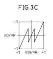
- the relation depicted in FIG. 3C holds between VIN/VR and VO/VR.
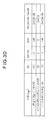
- the input voltage VIN (the compare voltage V CMP ), the digital output DO, the add/subtract coefficient DA1, the output voltage VDA1 of the sub-DAC 101, and the output voltage VO of the op amp OP1 are as depicted in FIG. 3D .
- VIN is in the range defined by -(1/4)*VR ⁇ VIN ⁇ -VR
- DO is -01
- DA is -1
- VDA1 is -VR
- VO is 2*VIN+VR.
- FIG. 4A is a circuit diagram illustrating one example of a 2.5-b MDAC in sampling mode and in hold mode, respectively, and FIG. 4B and FIG. 4C are diagrams for explaining the operation of the MDAC of FIG. 4A .
- the capacitor C1 n1 in the 2.5-b MDAC is divided into two capacitors C1 n11 and C1 n12 each of which is provided with a sub-DAC 101a or 101b and switches SWS11B and SWH11B or SWS12B and SWH12B.
- comparators CMP1 and CMP2 in FIG. 3A are replaced by six comparators CMP11 to CMP16, and six split voltages 5/8*VR, 3/8*VR, 1/8*VR, -1/8*VR, -3/8*VR, and -5/8*VR are applied to the respective comparators and compared with the input voltage VIN (V CMP ).
- the output signals from the respective comparators CMP11 to CMP16 are supplied to the logic unit LO1 via the respective flip-flops DFF11 to DFF16, and the logic unit LO1 outputs the digital output DO along with two add/subtract coefficients DA1 and DA2 that are supplied to the sub-DACs 101a and 101b.
- the switch control unit SWC1 sets the control signals for the switches SWS1A/2B/11B/12B and SWADCIN to "H", causing these switches to turn on.
- the switch control unit SWC1 sets the control signals for the switches SWH1A/2B/11B/12B and CLKADC to "L", causing the switches SWHlA/2B/11B/12B to turn off and disabling the flip-flops DFF1 to DFF16.
- the switch control unit SWC1 sets the control signals for the switches SWS1A/2B/11B/12B and SWADCIN to "L", causing these switches to turn off.
- the switch control unit SWC1 sets the control signals for the switches SWH1A/2B/11B/12B and CLKADC to "H". This causes the switches SWH1A/2B/11B/12B to turn on, and the flip-flops DFF1 to DFF6 are enabled to latch and hold the input data.
- the flip-flops DFF1 to DFF6 latch and hold the output signals of the corresponding comparators CMP11 to CMP16.
- the output signals from the flip-flops DFF1 to DFF6 are supplied to the logic unit LO1, and the logic unit LO1 outputs the digital output DO and the add/subtract coefficients DA1 and DA2.
- the add/subtract coefficients DA1 and DA2 are supplied to the sub-DACs 101b and 101a, respectively.
- the input voltage VIN (the compare voltage V CMP ), the digital output DO, the add/subtract coefficients DA1 and DA2, the output voltages VDA1 and VDA2 of the sub-DACs 101b and 101a, and the output voltage VO of the op amp OP1 are as depicted in FIG. 4C and FIG. 4D.
- VIN is in the range defined by -(5/8)*VR ⁇ VIN ⁇ -VR
- DO is -011
- DA is -3
- VDA2 is -VR
- VDA1 is -VR
- VO is 4*VIN+3*VR.
- FIG. 5 is a diagram for explaining the relationship between the operating speed in the computation mode (hold mode) of the MDAC and the current consumption of the op amp, and more specifically, the relationship between the speed of computation in the operation mode of the MDAC1 and the current consumption of the amplifier.
- a constant value CO is used as the reference value in FIG. 3A , FIG. 3B , FIG. 3C , FIG. 3D , FIG. 4A , FIG. 4B , and FIG. 4C .
- the signal amplification factor (m) is expressed by C1 s /C1 H .
- sampling capacitor C2 s in the next-stage MDAC may generally be multiplied by (1/m) relative to the signal amplification factor (m), but the limitation by the minimum capacitance value needs to be considered. That is, the following two points (A) and (B) need to be considered. [MATHEMATICAL 4]
- the term “without scaling” indicates that the capacitance of the MDAC remains the same at each stage.
- the conversion time increases by a factor of two or more compared with no load conditions; in particular, it is seen that when no scaling is applied to the capacitor C2 s in FIG. 5 , the decrease in conversion speed becomes more pronounced.
- the conversion speed decreases by a factor of six or more compared with no load conditions. This indicates that when the supply current to the amplifier (op amp) is held constant, the time taken to accomplish the conversion increases by a factor of two or more compared with no load conditions (the conversion speed decreases by a factor of two or more).
- the time taken to accomplish the conversion (computation) increases by a factor of two or more compared with the time taken when there is no such load. Furthermore, if no scaling is applied, the decrease in the conversion speed of the MDAC becomes more pronounced; further, as the number of bits increases, the decrease in speed becomes greater.
- FIG. 7 is a diagram for explaining the operation of the MDAC (switched capacitor circuit: SC circuit) during analog computation and subsequent stage sampling; more specifically, the operation in the earlier described analog computation mode (hold mode) is illustrated in simplified form.
- MDAC switched capacitor circuit: SC circuit
- the capacitors C1 MDAC and C1 H are connected (used). Further, the sampling capacitor C2 s in the SC circuit 12 (MDAC2) at the subsequent stage is coupled to the output of the operational amplifier (op amp) OP1 in order to sample its output voltage VO(0).
- the hold capacitor C1 H is connected between the output terminal and negative input terminal of the op amp OP1
- the computation capacitor C1 MDAC is connected between the output terminal of the sub-DA converter (101) and the negative input terminal of the op amp OP1.
- the sampling capacitor C2 s in the SC circuit 12 at the subsequent stage is coupled to the output terminal of the op amp OP1.
- the sampling capacitor C2 s in the SC circuit 12 at the subsequent stage is connected as the load for the op amp OP1, the supply current to the amplifier needs to be increased.
- FIG. 8A is a diagram for explaining the operation of an MDAC of a first embodiment during analog computation
- FIG. 8B is a diagram for explaining the operation of the MDAC of the first embodiment during subsequent stage sampling.
- the analog computation is performed by dividing it into two modes, the first-half operation mode and the second-half operation mode.
- the analog computation is performed in the SC circuit 11 (MDAC1) by disconnecting the sampling capacitor C2 s in the subsequent-stage SC circuit 12 (MDAC2).
- the feedback coefficient ⁇ is set to "1", i.e., full feedback, by disconnecting the computation capacitor C1 MDAC in the SC circuit 11, and the output voltage is stored on the sampling capacitor C2 s in the subsequent-stage SC circuit 12.
- FIG. 9A and FIG. 9B are diagrams for explaining the MDAC of the first embodiment and its operation with the conversion time (T) divided into four periods (1) to (4).
- the operation of the MDAC according to the first embodiment is characterized in that, in the period (1), the MDAC1 and the ADC1 (sub-AD converter) are not used, and the MDAC2 performs computation (hold: H).
- the output of the op amp OP2 in the MDAC2 is decoupled from the load (C3 s ) in the subsequent-stage MDAC (MDAC3) and the op amp OP2 is thus at no load.
- the ADC1 is used and the MDAC1 performs sampling (S), while the MDAC2 performs computation (full feedback operation).
- the MDAC2 and the ADC2 are not used, and the MDAC1 performs computation.
- the operation of the MDAC1 in the period (3) corresponds to the operation of the SC11 (MDAC1) described with reference to FIG. 8A .
- the capacitor C1 n1 acts as the computation capacitor C1 MDAC and the capacitor C1 n2 as the hold capacitor C1 H .
- the MDAC1 performs computation (full feedback operation), while on the other hand, the ADC2 is used and the MDAC2 performs sampling.
- the operation of the MDAC1 in the period (4) corresponds to the operation of the SC11 (MDAC1) described with reference to FIG. 8B .
- the MDAC of the first embodiment it becomes possible to enhance the speed of computation, reduce the power consumption of the amplifier, or reduce the footprint of the circuit, and so on.
- the ratio between the periods (1) and (2) may be varied as needed according to such factors as the operating speed of the circuit and the size of the capacitors used. Further, between the periods (1) and (2) (or the periods (3) and (4)), the supply current to the op amp OP1 may be set to different values.
- the control of the ratio between the periods (1) and (2) (or the periods (3) and (4)) and the control of the supply current to the op amp in the periods (1) and (2) (or the periods (3) and (4)) may be performed not only in the first embodiment but also in the second to fifth embodiments to be described later.
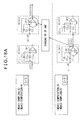
- FIG. 10A is a circuit diagram illustrating one example of the MDAC of the first embodiment
- FIG. 10B is a diagram for explaining the operation of the MDAC of FIG. 10A
- the MDAC illustrated in FIG. 10A and FIG. 10B is a 1.5-b MDAC (MDAC1).
- the circuit of the MDAC1 in the periods (1) to (4) in FIG. 10B corresponds to that of the MDAC1 in (1) to (4) depicted in FIG. 9A .
- reference character SWC1 designates a switch control unit which receives signals MCLK and SHSEL and outputs switch control signals; further, 101 is a sub-DAC, CMP1 and CMP2 are comparators, DFF1 and DFF2 are flip-flops, and LO1 is a logic unit.
- the MDAC1 (switched capacitor circuit) includes capacitors C1 n1 and C1 n2 (two or more internal capacitors), an op amp OP1 (one or more amplifiers), and switches SWS1A/1B/2A/2B, SWH1A/1B, SWH2A/2B, and SWADCIN (two or more internal switches).
- the MDAC1 is similar between the two, but differs in the way the switch control unit SWC1 controls the respective switches.
- the switch control unit SWC1 sets the control signals for the switches SWS1A/1B/2A/2B, SWH1A/1B, SWH2A/2B, and SWADCIN to a low level "L", causing these switches to turn off.
- the signal CLKADC is at "L”, so that the flip-flops DFF1 and DFF2 are disabled.
- the switch control unit SWC1 sets the control signals for the switches SWS1A/1B/2A/2B and SWADCIN to a high level "H", causing these switches to turn on.
- the control signals for the switches SWH1A/1B and SWH2A/2B and the signal CLKADC remain at "L".
- the switches SWS1A/1B/2A/2B and SWADCIN turn on, and the MDAC1 performs sampling (S). That is, the input voltage VIN (the compare voltage V CMP ) is coupled to the comparators CMP1 and CMP2 where it is compared with the reference voltages 1/4*VR and -1/4*VR, respectively, and the comparison results are supplied to the input terminals of the respective flip-flops DFF1 and DFF2.
- the input voltage VIN is sampled by the sampling capacitor C1 s (C1 n1 + C1 n2 ).
- the switch control unit SWC1 sets the control signals for the switches SWS1A/1B/2A/2B and SWADCIN to "L", causing these switches to turn off, and sets the control signals for the switches SWH1A/1B and SWH2A/2B to "H".
- the signal CLKADC is also set to "H”.
- the comparison results from the comparators CMP1 and CMP2 are latched into the flip-flops DFF1 and DFF2 and held therein. Since similar control is performed on the subsequent-stage MDAC2, the op amp OP1 is disconnected from the load (C2 s ) in the subsequent-stage MDAC2 and is thus held at no load.
- the hold capacitor C1 H (C1 n2 ) is connected between the output terminal and negative input terminal of the op amp OP1
- the computation capacitor C1 MDAC (C1 n1 ) is connected between the output terminal of the sub-DA converter 101 and the negative input terminal of the op amp OP1. Then, the op amp OP1 operates at no load with its output terminal decoupled from the sampling capacitor C2 s (C2 n1 + C2 n2 ) in the subsequent-stage MDAC2.
- the operation of the MDAC1 in the period (3) is the same as that described with reference to FIG. 8A , FIG. 9A , and FIG. 9B .
- the switch control unit SWC1 sets the control signal for the switches SWH1A/1B from “H” to "L” to turn off the switches SWH1A/1B thereby disconnecting the capacitor C1 n1 .
- the other switches SWS1A/1B/2A/2B, SWADCIN, and SWH2A/2B are each held in the same state as in the period (3).
- the MDAC1 performs full feedback operation.
- the operation of the MDAC1 in the period (4) is the same as that described with reference to FIG. 8A , FIG. 9A , and FIG. 9B .
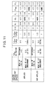
- the MDAC of the first embodiment is capable of improving the speed or the power consumption by about 33% when scaling is applied and by about 40% when no scaling is applied, as compared with the MDAC of FIG. 3A .
- the MDAC operating speed (T) when the MDAC operating speed (T) is the same, the power consumption (the op amp current I AMP ) may be reduced, while on the other hand, when the op amp current (I AMP : power consumption) is the same, the MDAC operating speed (T) may be enhanced.
- the circuit when applying the MDAC to a cyclic AD conversion circuit, the circuit may be designed by adjusting the switch timing (clock period) so as to increase the processing time in the starting or first-half period and reduce the processing time in the last or second-half period.
- the 2.5-b MDAC as a modified example of the first embodiment is capable of improving the speed or the power consumption by about 43% when scaling is applied and by about 63% when no scaling is applied, as compared with the MDAC of FIG. 4A .
- T*I AMP by giving priority to the operating speed (T) or the power consumption (I AMP ), whichever is desired, their magnitude may be designed appropriately as needed, as just described with reference to FIG. 11 ; further, the duration of each of the periods (1) to (4) may also be adjusted as needed.
- the duration of the first-half operation mode (period (3)) during analog computation of the MDAC (MDAC1) and the duration of the second-half operation mode (period (4)) are denoted by TL 1 and TL 2 , respectively, and the feedback ratio ⁇ in the first-half operation mode and that in the second-half operation mode are denoted by ⁇ 1 and ⁇ 2 , respectively.
- FIG. 13A and FIG. 13B are diagrams for explaining the MDAC of the second embodiment and its operation with the conversion time (T) divided into four periods (1) to (4).
- the operation of the MDAC according to the second embodiment is characterized in that, in the period (1), the MDAC1 is not used but the ADC1 is used. On the other hand, the MDAC2 performs computation (hold: H).
- the ADC1 is used in the period (1) so that in the period (1) the add/subtract coefficient DA1 is supplied to the sub-DAC not depicted (refer, for example, to the sub-DAC 101 in FIG. 3 ) in the MDAC1.
- the ADC1 supplies the add/subtract coefficient DA1 to the sub-DAC in the period (2).
- the MDAC1 performs sampling (S), while the MDAC2 performs computation (full feedback operation).
- the ADC1 continues to perform the same operation as that in the period (1).
- the MDAC2 is not used but the ADC2 is used, and the MDAC1 performs computation.
- the ADC2 is used in the period (3) so that in the period (3) the add/subtract coefficient DA2 is supplied to the sub-DAC (not depicted) in the MDAC2.
- the MDAC1 performs computation (full feedback operation), while on the other hand, the MDAC2 performs sampling.
- the ADC2 continues to perform the same operation as that in the period (3).
- the MDAC of the second embodiment aims to relax the constraints on the conversion speed of the comparators in the ADC1 (for example, the comparators CMP1 and CMP2 in FIG. 10A ) by utilizing, for example, the fact that the analog computation result of the MDAC1 is output in the two periods (1) and (2).
- the comparators CMP1 and CMP2 in the ADC1 need only perform the comparisons over the entire duration of the period (2) by using the final data obtained from the period (1); this serves to alleviate the need for higher operating speeds demanded of the comparators CMP1 and CMP2.
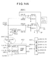
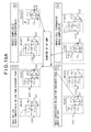
- FIG. 14A is a circuit diagram illustrating one example of the MDAC of the second embodiment
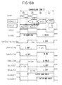
- FIG. 14B is a diagram for explaining the operation of the MDAC of FIG. 14A
- the MDAC illustrated in FIG. 14A and FIG. 14B is a 1.5-b MDAC (MDAC1).
- the circuit of the MDAC1 in the periods (1) to (4) in FIG. 14B corresponds to that of the MDAC1 in (1) to (4) in the above-described FIG. 13A .
- the MDAC (MDAC1) of the second embodiment differs from the MDAC1 of the first embodiment by the inclusion of a capacitor C s (CMP) which is provided between the switch SWASCIN and the ADC1 and which acts as a sampling capacitor C s in the period (1).
- CMP capacitor C s
- the MDAC1 (switched capacitor circuit) includes capacitors C1 n1 , C1 n2 , and C s (CMP) (two or more internal capacitors), the op amp OP1 (one or more amplifiers), and switches SWS1A/1B/2A/2B, SWH1A/1B, SWH2A/2B, and SWADCIN (two or more internal switches).
- the switch control unit SWC1 sets the control signals for the switches SWS1A/1B/2A/2B, SWH1A/1B, and SWH2A/2B to a low level "L”, causing these switches to turn off, and sets the control signal for the switch SWADCIN to a high level "H”, causing the switch SWADCIN to turn on.
- the signal CLKADC is at "L”, so that the flip-flops DFF1 and DFF2 are disabled.
- the difference from the embodiment earlier described with reference to FIG. 10A and FIG. 10B is that, in the period (1), the switch SWADCIN is turned on so that the compare voltage V CMP (the input voltage VIN) is sampled onto the sampling capacitor C s (CMP).
- the switch control unit SWC1 sets the control signal for the switches SWS1A/1B/2A/2B to "H", causing these switches to turn on, and sets the control signal for the switch SWADCIN to "L", causing the switch SWADCIN to turn off.
- the control signals for the switches SWH1A/1B and SWH2A/2B and the signal CLKADC remain at "L".
- the compare voltage V CMP sampled by the sampling capacitor C s (CMP) in the period (1) is coupled to the comparators CMP1 and CMP2 in the ADC1 where it is compared with the reference voltages 1/4*VR and -1/4*VR, respectively, and the comparison results are supplied to the input terminals of the respective flip-flops DFF1 and DFF2.
- the switch control unit SWC1 sets the control signals for the switches SWS1A/1B/2A/2B and SWADCIN to "L”, causing these switches to turn off, and sets the control signals for the switches SWH1A/1B and SWH2A/2B to "H", causing these switches to turn on.
- the signal CLKADC is also set to "H”.
- the comparison results from the comparators CMP1 and CMP2 are latched into the flip-flops DFF1 and DFF2 and held therein.
- the op amp OP1 is disconnected from the load (C2 s ) in the subsequent-stage MDAC2, but its output voltage VO1 is sampled onto the sampling capacitor C s (CMP) in the ADC2 at the subsequent stage.
- the switch control unit SWC1 sets the control signal for the switches SWH1A/1B from “H” to "L” to turn off the switches SWH1A/1B thereby disconnecting the capacitor C1 n1 .
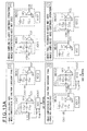
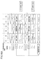
- FIG. 15A and FIG. 15B are diagrams for explaining the MDAC of the third embodiment and its operation with the conversion time (T) divided into four periods (1) to (4). Further, FIG. 16A is a circuit diagram illustrating one example of the MDAC of the third embodiment, and FIG. 16B is a diagram for explaining the operation of the MDAC of FIG. 16A .
- the third embodiment differs from the first embodiment in that the two comparators CMP1 and CMP2 in the first embodiment are replaced by one common comparator CMPO.
- the ADAC1 is provided with two switches SELADC1 and SELADC2, and the one comparator CMPO is made to perform the same functions as the comparators CMP1 and CMP2 of the first embodiment in the periods (1) and (2), respectively.
- the common signal CLKADC supplied to the clock terminals of the flip-flops DFF1 and DFF2 in the first embodiment is replaced by two separate signals CLKADC1 and CLKADC2 so that the activation of each of the flip-flops DFF1 and DFF2 is controlled independently of each other.
- the MDAC according to the third embodiment is characterized in that, in the period (1), the MDAC1 is not used but the ADC1 is used, while on the other hand, the MDAC2 performs computation (H).
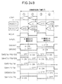
- the purpose of using the ADC1 in the period (1) is, for example, to compare the input voltage VIN (the compare voltage C CMP ) with the reference voltage 1/4*VR and output the result to the flip-flop DFF1.
- the ADC1 is used and the MDAC1 performs sampling (S), while the MDAC2 performs computation.
- the purpose of using the ADC1 in the period (2) is, for example, to compare the compare voltage C CMP with the reference voltage -1/4*VR and output the result to the flip-flop DFF2.
- the ADC1 in the third embodiment, in the period (1) the ADC1 is used to compare the compare voltage C CMP with the reference voltage 1/4*VR, and in the period (2) the ADC1 is used to compare the compare voltage C CMP with the reference voltage -1/4*VR. In this way, in the periods (1) and (2), the same comparator is used to compare the compare voltage with the respective reference voltages.
- the MDAC2 is not used but the ADC2 is used, while on the other hand, the MDAC1 performs computation. Then, in the period (4), the ADC2 is used, the MDAC1 performs computation, and the MDAC2 performs sampling.
- the purpose of using the ADC2 in the periods (3) and (4) is to compare the compare voltage at the subsequent stage with difference reference voltages, and the same comparator is used for this purpose.
- the compare voltage C CMP is applied to one input of the comparator CMP0 in the ADC1, and the reference voltage 1/4*VR or -1/4*VR, whichever is selected, is applied to the other input via the switch SELADC1 or SELADC2, respectively.
- the switches SELADC1 and SELADC2 are controlled by signals from the switch control unit SWC1.
- the MDAC1 (switched capacitor circuit) includes capacitors C1 n1 and C1 n2 (two or more internal capacitors), an op amp OP1 (one or more amplifiers), and switches SWS1A/1B/2A/2B, SWH1A/1B, SWH2A/2B, and SWADCIN (two or more internal switches).
- the switch control unit SWC1 sets the control signals for the switches SWS1A/1B/2A/2B, SWH1A/1B, SWH2A/2B, and SELADC2 to "L", causing these switches to turn off, and sets the control signals for the switches SWADCIN and SELADC1 to "H", causing these switches to turn on.
- the compare voltage C CMP (the input voltage VIN) and the reference voltage 1/4*VR selected via the switch SELADC1 are applied to the comparator CMP0 which then compare these voltages and outputs the result of the comparison.
- the signals CLKADC1 and CLKADC2 are both "L", so that the flip-flops DFF1 and DFF2 are disabled.
- the switch control unit SWC1 sets the control signals for the switches SWS1A/1B/2A/2B and SELADC2 to "H", causing these switches to turn on, and sets the control signal for the switch SELADC1 to "L”, causing the switch SELADC1 to turn off.
- the other switches are each held in the same state as in the period (1).
- the signal CLKRDC1 changes from “L” to "H", so that the flip-flop DFF1 is enabled to latch and hold the result of the comparison made between the compare voltage C CMP and the reference voltage 1/4*VR by the comparator CMP0.
- the comparator CMP0 compares the compare voltage C CMP with the reference voltage -1/4*VR applied via the switch SELADC1.
- the switch control unit SWC1 sets the control signals for the switches SWS1A/1B/2A/2B, SWADCIN, and SELADC2 to "L", causing these switches to turn off, and sets the control signals for the switches SWH1A/1B and SWH2A/2B to "H", causing these switches to turn on.
- the signal CLKADC2 changes from “L” to "H”, so that the flip-flop DFF2 is enabled to latch and hold the result of the comparison made between the compare voltage C CMP and the reference voltage -1/4*VR by the comparator CMP0.
- the result of the comparison between the compare voltage C CMP and the reference voltage 1/4*VR, held in the flip-flop DFF1 and the result of the comparison between the compare voltage C CMP and the reference voltage -1/4*VR, held in the flip-flop DFF2, are supplied to the logic unit LO1 which performs a prescribed logic operation between them.
- the switch control unit SWC1 sets the control signal for the switches SWH1A/1B from "H” to "L” to turn off the switches SWH1A/1B.
- the operation in each of the periods (1) to (4) is apparent from the description given in the first and second embodiments, and therefore will not be further described herein.
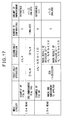
- FIG. 17 is a diagram depicting the number of comparators needed in the MDAC of the third embodiment for comparison with the number of comparators needed in each of the MDACs depicted in FIG. 3A and FIG. 4A .
- the comparators CMP1 and CMP2 in the ADC may be replaced by one common comparator CMP0, thus halving the number of comparators.
- the number of comparators CMP11 to CMP16 (six comparators) in FIG. 14 may be reduced by one half, i.e., to three, when the third embodiment is applied.
- FIG. 18A and FIG. 18B are diagrams for explaining another example of the MDAC and its operation; in the illustrated MDAC configuration, provisions are made to share one common op amp in order to reduce the footprint and power consumption of a pipelined AD conversion circuit.
- the MDAC configuration depicted in FIG. 18A and FIG. 18B is characterized in that the op amps OP1 and OP2 in the MDACs depicted in FIG. 2A and FIG. 2B are substituted by one common op amp (OP1) .
- the op amp is not needed in the sampling mode (the period (1)+(2): S) that samples the input voltage VIN, but is needed only in the hold mode (the period (3)+(4): H) that performs computation.
- the op amp is used only in the hold mode (the period (1)+(2): H) that performs computation.
- the op amp (OP1) is used as the op amp 2 for the MDAC2 during the period (1)+(2)
- the op amp OP1 is used as the op amp 1 for the MDAC1 during the period (3)+(4).
- the comparators in the sub-AD converts ADC1 and ADC2 not depicted may also be substituted by one common comparator.
- the capacitors in the respective MDACs (the computation capacitor C1 n1 , C1 n2 in the MDAC1 and the computation capacitor C2 n1 , C2 n2 in the MDAC2) need to be provided separately, and it is therefore not possible to share the same capacitor between them.
- FIG. 19A and FIG. 19B are diagrams for explaining the MDAC of the earlier described first embodiment and its operation.
- C1 n1 is not used in the periods (1) and (4)
- C1 n2 is not used in the period (1)
- C2 n1 is not used in the periods (2) and (3)
- C2 n2 is not used in the period (3).
- the capacitors are also shared by utilizing the periods in which the respective capacitors in the MDACs (C1 n1 and C1 n2 in the MDAC1 and C2 n1 and C2 n2 in the MDAC2) are not used.
- the MDAC circuit configuration more specifically, in the case of the 1.5-b MDAC, for example, two types of circuit configuration are possible, that is, the first configuration example (type I) and the second configuration example (type II).
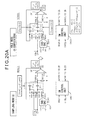
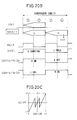
- FIG. 20A is a circuit diagram illustrating the first configuration example (type I) of the 1.5-b MDAC in sampling mode and in hold mode, respectively, and FIG. 20B, FIG. 20C , and FIG. 20D are diagrams for explaining the operation of the MDAC of FIG. 20A .
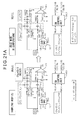
- FIG. 21A is a circuit diagram illustrating the second configuration example (type II) of the 1.5-b MDAC in sampling mode and in hold mode, respectively
- FIG. 21B, FIG. 21C , and FIG. 21D are diagrams for explaining the operation of the MDAC of FIG. 21A .
- FIG. 20A , FIG. 20B , FIG. 20C , and FIG. 20D correspond to the previously described FIG. 3A , FIG. 3B , FIG. 3C , and FIG. 3D , except that the signals associated with the ADC1 (sub-AD converter) in the MDAC1 in FIG. 3A , FIG. 3B , FIG. 3C , and FIG. 3D are omitted.
- ADC1 sub-AD converter
- the MDACs of the first to third embodiments illustrated in FIG. 8A, FIG. 8B , FIG. 9A , FIG. 9B , FIG. 10A , FIG. 10B , FIG. 12 , FIG. 13A , FIG. 13B , FIG. 14A , FIG. 14B , FIG. 15A , FIG. 15B , FIG. 16A , FIG. 16B , and FIG. 17 are each based on the type I circuit, but it is also possible to apply the MDACs of the first to third embodiments to the type II circuit.
- the switch control unit SWC1 sets the control signal for the switches SWS1A/11B/2A/12B to a high level "H", causing these switches to turn on.
- the switch control unit SWC1 sets the control signal for the switches SWH1A/11B/12B/2B to a low level "L". This causes the switches SWH1A/11B/12B/2B to turn off.
- the sampling capacitor C1 s on which the MDAC1 samples the input signal VIN
- the switch control unit SWC1 sets the control signal for the switches SWS1A/11B/12B/2B to "L", causing these switches to turn off.
- the switch control unit SWC1 sets the control signal for the switches SWH1A/11B/12B/2B to "H". This causes the switches SWH1A/11B/12B/2B to turn on.
- FIG. 21C and FIG. 21D are the same as the earlier given FIG. 20C and FIG. 20D , respectively.
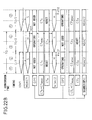
- FIG. 22A and FIG. 22B are diagrams for explaining the basic operation of the MDAC of the second configuration example (type II); the above-described FIG. 21A and FIG. 21B are redrawn here in an easier to understand manner.
- MDAC configuration depicted in FIG. 22A one common op amp (OP1) is shared between two MDACs (MDAC1 and MDAC2).
- C1 H CO/m
- C2 H CO/m
- m represents the signal amplification factor
- the capacitor C1 s in the MDAC1 and the capacitors C2 MDAC and C2 H in the MDAC2 are used, while the capacitor C1 H in the MDAC1 is reset.
- the capacitors C1 MDAC and C1 H in the MDAC1 and the capacitor C2 s in the MDAC2 are used, while the capacitor C2 H in the MDAC2 is reset.
- the op amp (OP1: common op amp) is shared between the two MDACs (MDAC1 and MDAC2).
- MDAC1 and MDAC2 MDACs
- the same capacitor is shared between the MDAC1 and the MDAC2 in order to further reduce the footprint of the switched capacitor circuit or AD conversion circuit.
- FIG. 23A and FIG. 23B are diagrams for explaining the MDAC of the fourth embodiment and its operation.
- the MDAC of the fourth embodiment is a MDAC of the second configuration example (type II), and is controlled by dividing the conversion time T into four periods (1) to (4), as in the case of the MDACs of the earlier described first to third embodiments.
- the capacitor CSC is used as C2 MDAC in the period (1), as C1 s in the period (2), as C1 MDAC in the period (3), and as C2 s in the period (4).
- the hold capacitors C1 H and C2 H need to be provided exclusively for the MDAC1 and the MDAC2, respectively, but the sampling capacitors C1 s and C2 s and computation capacitors C1 MDAC and C2 MDAC in the MDAC1 and MDAC2 may be replaced by one common capacitor.
- the op amp (common op amp OP1) is shared between the MDAC1 and the MDAC2 in the same manner as earlier described with reference to FIG. 22A and FIG. 22B .
- the value of the sampling capacitor in the MDAC at the subsequent stage may be made smaller than the value of the sampling capacitor in the MDAC at its preceding stage (for example, the capacitor C1 s in the MDAC1). That is, the sampling capacitor (C2 s ) in the MDAC at the subsequent stage may be formed using a portion of the sampling capacitor (C1 s in the MDAC at its preceding stage.
- FIG. 24A is a circuit diagram illustrating one example of the MDAC of the fourth embodiment
- FIG. 24B is a diagram for explaining the operation of the MDAC of FIG. 24A .
- reference characters CSC11 and CSC12 designate the common capacitor (CSC) shared for use, while CH1 designates the hold capacitor (C1 H ) when used for the first MDAC (MDAC1) and CH2 designates the hold capacitor (C2 H ) when used for the second MDAC (MDAC2).
- the MDAC0 (switched capacitor circuit) includes the capacitors CH1, CH2, CSC 11, and CSC12 (two or more internal capacitors) and the op amp OP0 (one or more amplifiers).
- the MDAC0 further includes switches SWVIN1, SWVIN2, SWSC1A/11B/12B, SWHC1A/11B/12B, SWHH1A/1B, SWSH2A/2B, and SWHH2A/2B (two or more internal switches).
- the switch control unit SWC1 sets the control signals for the switches SWVIN1, SWHC1A/11B/12B, and SWHH2A/2B to a high level "H", causing these switches to turn on.
- the switch control unit SWC1 sets the control signals for the switches SWVIN2, SWSC1A/11B/12B, SWSH1A/1B, SWHH1A/1B, and SWSH2A/2B to a low level "L", causing these switches to turn off.
- the capacitor CSC11 acts as the computation capacitor C2 MDAC for the second MDAC (MDAC2), as illustrated in the period (1) of FIG. 23A .
- the capacitor CH2 is connected so as to act as the hold capacitor C2 H for the second MDAC (MDAC2).
- the switch control unit SWC1 sets the control signals for the switches SWSC1A/11B/12B and SWSH1A/1B to "H", causing these switches to turn on, and sets the control signal for the switches SWHC1A/11B/12B to "L”, causing these switches to turn off.
- the other switches SWVIN1, SWVIN2, SWHH1A/1B, SWSH2A/2B, and SWHH2A/2B are each held at the same level as in the period (1).
- the capacitors CSC11 and CSC12 act as the sampling capacitor C1 s for the first MDAC (MDAC1), as illustrated in the period (2) of FIG. 23A .
- the capacitor CH2 remains connected so as to act as the hold capacitor C2 H for the second MDAC (MDAC2), while the capacitor CH1 is reset.
- the switch control unit SWC1 sets the control signals for the switches SWVIN2, SWHC1A/11B/12B, and SWHH1A/1B to "H", causing these switches to turn on. Further, the switch control unit SWC1 sets the control signals for the switches SWVIN1, SWSC1A/11B/12B, SWSH1A/1B, and SWSH2A/2B to "L", causing these switches to turn off. In the period (3), the control signal for the SWSH2A/2B is held at the same level as in the period (2).
- the capacitor CSC11 acts as the computation capacitor C1 MDAC for the first MDAC (MDAC1), as illustrated in the period (3) of FIG. 23A .
- the capacitor CH1 is connected so as to act as the hold capacitor C1 H for the first MDAC (MDAC1).
- the switch control unit SWC1 sets the control signals for the switches SWSC1A/11B/12B and SWSH2A/2B to "H", causing these switches to turn on, and sets the control signal for the switches SWHC1A/11B/I2B to "L”, causing these switches to turn off.
- the capacitors CSC11 and CSC12 act as the sampling capacitor C2 s for the second MDAC (MDAC2), as illustrated in the period (4) of FIG. 23A .
- the capacitor CH1 remains connected so as to act as the hold capacitor C1 H for the first MDAC (MDAC1), while the capacitor CH2 is reset.
- the op amp OP1 (common op amp) may be shared between the MDAC1 and the MDAC2 in the same manner as earlier described with reference to FIG. 22A and FIG. 22B .
- the capacitor may also be shared between the two MDACs, thus making is possible to further reduce the footprint of the switched capacitor circuit or AD conversion circuit.
- scaling may be applied, and the sampling capacitor C2 s in the MDAC2 at the subsequent stage, for example, may be made smaller in size than the sampling capacitor C1 s in the MDAC1 at its preceding stage.
- the sampling capacitor C2 s in the MDAC2 at the subsequent stage may be formed using a portion of the sampling capacitor C1 s in the MDAC1 at its preceding stage.
- the double-sampling AD conversion circuit includes two paralleled MDACs and operates them in interleaved fashion thereby aiming to double the conversion speed of the AD conversion circuit without increasing the power consumption.
- FIG. 25 is a diagram for explaining the basic operation of the MDAC of the first configuration example (type I) as applied in the parallel MDAC system.
- the double-sampling MDAC (parallel MDAC) system depicted here corresponds, for example, to one that performs processing by paralleling two MDACs (MDAC1 and MDAC2) which perform processing in time sequential fashion as described above.
- the double-sampling MDAC system depicted in FIG. 25 may be implemented, for example, by reconfiguring the MDAC1 and MDAC2 in the earlier described FIG. 18A to operate as MDAC1(E: Even mode) and MDAC2 (O: Odd mode), respectively.
- the MDAC1(E) samples the input voltage VIN1(E) by using the sampling capacitor C1 n1 (E)+C1 n2 (E), while on the other hand, the MDAC1(O) performs computation.
- the computation capacitor in the MDAC1(O) is C1 n1 (O), and the hold capacitor is C1 n2 (O).
- the op amp OP1(O) in the MDAC1(O) that performs computation is used, and the op amp OP1(E) in the MDAC1(E) that performs the sampling is not used.
- the MDAC1(E) performs computation, and the MDAC1(0) samples the input voltage VINl(O) by using the sampling capacitor C1 n1 (O)+C1 n2 (O).
- the computation capacitor in the MDAC1(E) is C1 n1 (E), and the hold capacitor is C1 n2 (E).
- the op amp OP1(E) in the MDAC1(E) that performs computation is used, and the op amp OP1(O) in the MDAC1(O) that performs the sampling is not used.
- the op amp (OP1(E)) is configured to act at the op amp OP1(O) in the period (1)+(2) and as the op amp OP1(E) in the period (3)+(4).
- the op amp may thus be shared between the MDAC1(E) and the MDAC1(O), it is not possible to share the capacitors in the parallel MDAC configuration of type I depicted in FIG. 25 .
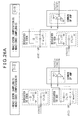
- FIG. 26A and FIG. 26B are diagrams for explaining the basic operation of the MDAC of the second configuration example (type II) as applied in the parallel MDAC system.
- the double-sampling MDAC (parallel MDAC) system depicted in FIG. 26A and FIG. 26B may be implemented, for example, by reconfiguring the MDAC1 and MDAC2 in the earlier described FIG. 22A and FIG. 22B to operate as MDAC1(E) and MDAC2(O), respectively.
- the capacitor C1 s (E) in the MDAC1(E) and the capacitors C1 MDAC (O) and C1 H (O) in the MDAC1(O) are used, while the capacitor C1 H (E) in the MDAC1(E) is reset.
- the capacitors C1 MDAC (E) and C1 H (E) in the MDAC1(E) and the capacitor C1 s (O) in the MDAC1(O) are used, while the capacitor C1 H (O) in the MDAC1(O) is reset.
- the op amp (OP1: common op amp) is shared between the two MDACs (MDAC1(E) and MDAC1(O)).
- MDAC1(E) MDAC1(E)
- MDAC1(O) MDAC1(O)
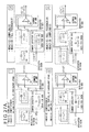
- FIG. 27A and FIG. 27B are diagrams for explaining the MDAC of the fifth embodiment and its operation; the MDAC illustrated here is a MDAC of the second configuration example (type II).
- the MDAC of the fifth embodiment is implemented by applying the MDAC of the fourth embodiment to a double-sampling MDAC (parallel MDAC) system. More specifically, in FIG. 27A , FIG. 27B , FIG. 28A , and FIG. 28B , the MDAC1 and MDAC2 in the earlier described FIG. 23A , FIG. 23B , FIG. 24A , and FIG. 24B are reconfigured to operate as MDAC1(E) and MDAC1(O), respectively.
- the capacitor CSC is used as C1 MDAC (O) in the period (1), as C1 s (E) in the period (2), as C1 MDAC (E) in the period (3), and as C1 s (O) in the period (4).
- the hold capacitors C1 H (E) and C1 H (O) need to be provided exclusively for the MDAC1(E) and the MDAC1(O), respectively.
- the sampling capacitors C1 s (E) and C1 s (O) and computation capacitors C1 MDAC (E) and C1 MDAC (O) in the MDAC1(E) and MDAC1(0) may be replaced by one common capacitor.
- the op amp (common op amp OP1(E)) is shared between the MDAC1(E) and the MDAC1 (O) in the same manner as earlier described.
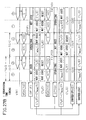
- FIG. 28A is a circuit diagram illustrating one example of the MDAC of the fourth embodiment
- FIG. 28B is a diagram for explaining the operation of the MDAC of FIG. 28A .
- reference characters CSC11 and CSC12 designate the common capacitor (CSC) shared for use, while CH1E designates the hold capacitor (C1 H (E)) when used for the first MDAC (MDAC1(E)) and CH1O designates the hold capacitor (C1 H (O)) when used for the second MDAC (MDAC1(0)).
- the switch control unit SWC1 sets the control signals for the switches SWVIN1E, SNHC1A/11B/12B, and SWHH2A/2B to a high level "H", causing these switches to turn on.
- the switch control unit SWC1 sets the control signals for the switches SWVIN1O, SWSC1A/11B/12B, SWSH1A/1B, SWHH1A/1B, and SWSH2A/2B to a low level "L", causing these switches to turn off.
- the capacitor CSC11 acts as the computation capacitor C1 MDAC (O) for the second MDAC (MDAC1(O)), as illustrated in the period (1) of FIG. 27A .
- the capacitor CH1O is connected so as to act as the hold capacitor C1 H (O) for the second MDAC (MDAC1(O)).
- the switch control unit SWC1 sets the control signals for the switches SWSC1A/11B/12B and SWSH1A/1B to "H", causing these switches to turn on, and sets the control signal for the switches SWHC1A/11B/12B to "L”, causing these switches to turn off.
- the other switches SWVIN1E, SWVIN1O, SWHH1A/1B, SWSH2A/2B, and SWHH2A/2B are each held at the same level as in the period (1).
- the capacitors CSC11 and CSC12 act as the sampling capacitor C1 s (E) for the first MDAC (MDAC1(E)), as illustrated in the period (2) of FIG. 27A .
- the capacitor CH10 remains connected so as to act as the hold capacitor C1 H (O) for the second MDAC (MDAC1(O)), while the capacitor CH1E is reset.
- the switch control unit SWC1 sets the control signals for the switches SWVIN1O, SWHC1A/11B/12B, and SWHH1A/1B to "H", causing these switches to turn on. Further, the switch control unit SWC1 sets the control signals for the switches SWVIN1E, SWSC1A/11B/12B, SWSH1A/1B, and SWSH2A/2B to "L", causing these switches to turn off. In the period (3), the control signal for the SWSH2A/2B is held at the same level as in the period (2).
- the capacitor CSC11 acts as the computation capacitor C1 MDAC (E) for the first MDAC (MDAC1(E)), as illustrated in the period (3) of FIG. 27A .
- the capacitor CH1E is connected so as to act as the hold capacitor C1 H (E) for the first MDAC (MDAC1(E)).
- the switch control unit SWC1 sets the control signals for the switches SWSC1A/11B/12B and SWSH2A/2B to "H", causing these switches to turn on, and sets the control signal for the switches SWHC1A/11B/12B to "L”, causing these switches to turn off.
- the capacitors CSC11 and CSC12 act as the sampling capacitor C1 s (O) for the second MDAC (MDAC1(O)), as illustrated in the period (4) of FIG. 27A .
- the capacitor CH1E remains connected so as to act as the hold capacitor C1 H (E) for the first MDAC (MDAC1(E)), while the capacitor CH1O is reset.
- the op amp OPl(E) may be shared between the MDAC1(E) and the MDAC1(O) in the same manner as earlier described.
- the capacitor may also be shared between the two MDACs, thus making is possible to further reduce the footprint of the switched capacitor circuit or AD conversion circuit.
- FIG. 29 is a diagram illustrating the performance of the MDACs of the fourth and fifth embodiments for comparison with the performance of the MDACs depicted in FIG. 22A and 26A .
- the MDAC of the fourth embodiment achieves, by virtue of the capacitor sharing, a reduction in capacitance, i.e., the footprint of the capacitors (the circuit), by about 33% in the case of no scaling applied and about 22% in the case of scaling applied.
- FIG. 30 is a block diagram schematically illustrating one example of a pipelined AD conversion circuit to which the MDAC of each embodiment is applied
- FIG. 31 is a block diagram schematically illustrating one example of a cyclic AD conversion circuit to which the MDAC of each embodiment is applied.
- the MDAC of any one of the first to fifth embodiments described above may be applied, for example, as an MDAC in a cascade of MDAC circuits 202-1 to 202-(n-1) such as used in the pipelined AD conversion circuit 200 of FIG. 30 .
- the pipelined AD conversion circuit 200 includes a sample-and-hold (S/H) circuit 201, (n-1) stages of MDAC circuits 202-1 to 202-(n-1), a flash ADC 203 at the last stage, and a logic operation circuit (digital correction circuit) 204.
- S/H sample-and-hold
- n-1 stages of MDAC circuits 202-1 to 202-(n-1)
- flash ADC 203 at the last stage
- a logic operation circuit digital correction circuit
- the sample-and-hold circuit 201 samples the input voltage VIN and holds it, and supplies its output signal to the MDAC circuits 202-1 to 202-(n-1).
- the logic operation circuit 204 receives the output signals DB(1) to DB(n-1) of the MDAC circuits 202-1 to 202-(n-1) as well as the output signal DB(n) of the flash ADC 203 at the last stage, and produces an output code (ADC output) by analog-to-digital converting the input voltage VIN with a resolution corresponding to the number of stages of the MDAC circuits.
- the MDAC of any one of the first to fifth embodiments described above may be applied, for example, as an MDAC circuit 303 such as used in the cyclic AD conversion circuit 300 of FIG. 31 .
- the cyclic AD conversion circuit 300 includes, in addition to the MDAC circuit 303, a switch 301, a sample-and-hold (S/H) circuit 302, and a logic operation circuit 304.
- the sample-and-hold circuit 302 may be omitted.
- the signal DB(i) output from the MDAC circuit 303 in each cycle is supplied to the logic operation circuit 304, and the logic operation circuit 304 produces an output code (ADC output) by analog-to-digital converting the voltage with a resolution corresponding to the number of cycles through the MDAC circuit.
- the MDACs of the first to fifth embodiments may be applied not only to pipelined AD conversion circuits and cyclic AD conversion circuits but also extensively to various other circuits such as DA converts and filters.
Landscapes
- Engineering & Computer Science (AREA)
- Theoretical Computer Science (AREA)
- Physics & Mathematics (AREA)
- Nonlinear Science (AREA)
- Analogue/Digital Conversion (AREA)
- Amplifiers (AREA)
- Manipulation Of Pulses (AREA)
Abstract
Description
- The embodiments discussed herein are related to a switched capacitor circuit and an AD conversion circuit.
- Switched capacitor circuits are widely used in high-resolution, low-power AD (Analog-to-Digital) converters, DA (Digital-to-Analog) converters, filters, etc.
- More specifically, a switched capacitor circuit includes a capacitor, a switch, and an amplifier, and this type of circuit is applied, for example, to an MDAC (Multiplying DAC) or the like used as a basic building block in a pipelined AD conversion circuit or a cyclic AD conversion circuit.
- In this patent specification, an AD conversion circuit and a switched capacitor circuit (MDAC) to be used therein will be described as examples, but as stated above, the switched capacitor circuit is also applicable to a DA converter, a filter, etc.
- Various forms of pipelined AD conversion circuits employing switched capacitor circuits have been proposed.
-
- Non-Patent Document 1: Shoji Kawahito, "Low-Power Design of Pipeline A/D converters," IEEE Custom Integrated Circuits Conference 2006, pp. 505-512, 2006
- Non-Patent Document 2: Kunihiko Gotoh et al., "3 STATES LOGIC CONTROLLED CMOS CYCLIC A/D CONVERTER," IEEE Custom Integrated Circuits Conference 1986, pp. 366-369, 1986
- Non-Patent Document 3: Chin-Chen Lee, "A NEW SWITCHED-CAPACITOR REALIZATION FOR CYCLIC ANALOG-TO-DIGITAL CONVERTER," IEEE 1983, pp. 1261-1265, 1983
- As described above, the switched capacitor circuit is applied, for example, to an MDAC or the like in a pipelined AD conversion circuit.
- With the recent proliferation of high-functionality digital signal processing in various systems, it has become increasingly important to provide an AD conversion circuit capable of high-resolution and high-speed processing. In the field of portable apparatus, for example, there has also developed a need to further reduce power consumption while also reducing the area occupied by the circuit.
- According to one embodiment, there is provided a switched capacitor circuit, included in a circuit including a load circuit, configured to be operable in two or more kinds of operation modes including a first operation mode and a second operation mode.
- The switched capacitor circuit includes two or more internal capacitors, one or more amplifiers, and two or more internal switches. The load circuit includes a sampling capacitor, provided at a stage subsequent to the switched capacitor circuit, and a sampling switch for controlling connection/disconnection of the sampling capacitor.
- In the first operation mode that precedes the second operation mode, the sampling switch at the subsequent stage is turned off, thereby decoupling an output voltage of the switched capacitor circuit from the sampling capacitor at the subsequent stage, and the switched capacitor circuit performs computation.
- In the second operation mode that follows the first operation mode, the sampling switch at the subsequent stage is turned on, thereby sampling the output voltage of the switched capacitor circuit onto the sampling capacitor.
- In the first operation mode, the switched capacitor circuit performs control to disconnect one or more of the internal capacitors by the internal switches.
- The switched capacitor circuit and AD conversion circuit disclosed herein offers the effect of being able to enhance the speed of computation, reduce the power consumption of the amplifier, or reduce the footprint of the circuit, and so on.
-
- [
FIG. 1A ] is a block diagram illustrating one example of an AD conversion circuit. - [
FIG. 1B ] is a diagram (part 1) for explaining the operation of the AD conversion circuit ofFIG. 1A . - [
FIG. 1C ] is a diagram (part 2) for explaining the operation of the AD conversion circuit ofFIG. 1A . - [
FIG. 2A ] is a diagram (part 1) for explaining one example of MDAC and its operation. - [
FIG. 2B ] is a diagram (part 2) for explaining one example of MDAC and its operation. - [
FIG. 2C ] is a diagram (part 3) for explaining one example of MDAC and its operation. - [
FIG. 3A ] is a circuit diagram illustrating one example of a 1.5-b MDAC in sampling mode and in hold mode, respectively. - [
FIG. 3B ] is a diagram (part 1) for explaining the operation of the MDAC ofFIG. 3A . - [
FIG. 3C ] is a diagram (part 2) for explaining the operation of the MDAC ofFIG. 3A . - [
FIG. 3D ] is a diagram (part 3) for explaining the operation of the MDAC ofFIG. 3A . - [
FIG. 4A ] is a circuit diagram illustrating one example of a 2.5-b MDAC in sampling mode and in hold mode, respectively. - [
FIG. 4B ] is a diagram (part 1) for explaining the operation of the MDAC ofFIG. 4A . - [
FIG. 4C ] is a diagram (part 2) for explaining the operation of the MDAC ofFIG. 4A . - [
FIG. 5 ] is a diagram for explaining the relationship between the operating speed in the computation mode of the MDAC and the current consumption of an op amp. - [
FIG. 6 ] is a diagram illustrating performance comparisons for MDAC-type AD conversion circuits under no load conditions. - [
FIG. 7 ] is a diagram for explaining the operation of the MDAC during analog computation and subsequent stage sampling. - [
FIG. 8A ] is a diagram for explaining the operation of an MDAC of a first embodiment during analog computation. - [
FIG. 8B ] is a diagram for explaining the operation of the MDAC of the first embodiment during subsequent stage sampling. - [
FIG. 9A ] is a diagram (part 1) for explaining the MDAC of the first embodiment and its operation. - [
FIG. 9B ] is a diagram (part 2) for explaining the MDAC of the first embodiment and its operation. - [
FIG. 10A ] is a circuit diagram illustrating one example of the MDAC of the first embodiment. - [
FIG. 10B ] is a diagram for explaining the operation of the MDAC ofFIG. 10A . - [
FIG. 11 ] is a diagram illustrating the performance of the MDAC of the first embodiment for comparison with the MDAC depicted inFIG. 3A . - [
FIG. 12 ] is a diagram illustrating the performance of a modified example of the MDAC of the first embodiment for comparison with the MDAC depicted inFIG. 4A . - [
FIG. 13A ] is a diagram (part 1) for explaining an MDAC according to a second embodiment and its operation. - [
FIG. 13B ] is a diagram (part 2) for explaining the MDAC of the second embodiment and its operation. - [
FIG. 14A ] is a circuit diagram illustrating one example of the MDAC of the second embodiment. - [
FIG. 14B ] is a diagram for explaining the operation of the MDAC ofFIG. 14A . - [
FIG. 15A ] is a diagram (part 1) for explaining an MDAC according to a third embodiment and its operation. - [
FIG. 15B ] is a diagram (part 2) for explaining the MDAC of the third embodiment and its operation. - [
FIG. 16A ] is a circuit diagram illustrating one example of the MDAC of the third embodiment. - [
FIG. 16B ] is a diagram for explaining the operation of the MDAC ofFIG. 16A . - [
FIG. 17 ] is a diagram depicting the number of comparators needed in the MDAC of the third embodiment for comparison with the number of comparators needed in each of the MDACs depicted inFIG. 3A andFIG. 4A . - [
FIG. 18A ] is a diagram (part 1) for explaining another example of the MDAC and its operation. - [
FIG. 18B ] is a diagram (part 2) for explaining that other example of the MDAC and its operation. - [
FIG. 19A ] is a diagram (part 1) for explaining the MDAC of the earlier described first embodiment and its operation. - [
FIG. 19B ] is a diagram (part 2) for explaining the MDAC of the earlier described first embodiment and its operation. - [
FIG. 20A ] is a circuit diagram illustrating a first configuration example of the 1.5-b MDAC in sampling mode and in hold mode, respectively. - [
FIG. 20B ] is a diagram (part 1) for explaining the operation of the MDAC ofFIG. 20A . - [
FIG. 20C ] is a diagram (part 2) for explaining the operation of the MDAC ofFIG. 20A . - [
FIG. 20D ] is a diagram (part 3) for explaining the operation of the MDAC ofFIG. 20A . - [
FIG. 21A ] is a circuit diagram illustrating a second configuration example of the 1.5-b MDAC in sampling mode and in hold mode, respectively. - [
FIG. 21B ] is a diagram (part 1) for explaining the operation of the MDAC ofFIG. 21A . - [
FIG. 21C ] is a diagram (part 2) for explaining the operation of the MDAC ofFIG. 21A . - [
FIG. 21D ] is a diagram (part 3) for explaining the operation of the MDAC ofFIG. 21A . - [
FIG. 22A ] is a diagram (part 1) for explaining the basic operation of the MDAC of the second configuration example. - [
FIG. 22B ] is a diagram (part 2) for explaining the basic operation of the MDAC of the second configuration example. - [
FIG. 23A ] is a diagram (part 1) for explaining an MDAC according to a fourth embodiment and its operation. - [
FIG. 23B ] is a diagram (part 2) for explaining the MDAC of the fourth embodiment and its operation. - [
FIG. 24A ] is a circuit diagram illustrating one example of the MDAC of the fourth embodiment. - [
FIG. 24B ] is a diagram for explaining the operation of the MDAC ofFIG. 24A . - [
FIG. 25 ] is a diagram for explaining the basic operation of the MDAC of the first configuration example as applied in a parallel MDAC system. - [
FIG. 26A ] is a diagram (part 1) for explaining the basic operation of the MDAC of the second configuration example as applied in the parallel MDAC system. - [
FIG. 26B ] is a diagram (part 2) for explaining the basic operation of the MDAC of the second configuration example as applied in the parallel MDAC system. - [
FIG. 27A ] is a diagram (part 1) for explaining an MDAC according to a fifth embodiment and its operation. - [
FIG. 27B ] is a diagram (part 2) for explaining the MDAC of the fifth embodiment and its operation. - [
FIG. 28A ] is a circuit diagram illustrating one example of the MDAC of the fifth embodiment. - [
FIG. 28B ] is a diagram for explaining the operation of the MDAC ofFIG. 28A . - [
FIG. 29 ] is a diagram illustrating the performance of the MDACs of the fourth and fifth embodiments for comparison with the performance of the MDACs depicted inFIG. 22A and26A . - [
FIG. 30 ] is a block diagram schematically illustrating one example of a pipelined AD conversion circuit to which the MDAC of each embodiment is applied. - [
FIG. 31 ] is a block diagram schematically illustrating one example of a cyclic AD conversion circuit to which the MDAC of each embodiment is applied. - Before describing the embodiments in detail, switched capacitor circuits and AD conversion circuits and their associated problems will be described below.
-
FIG. 1A is a block diagram illustrating one example of an AD conversion circuit, andFIG. 1B andFIG. 1C are diagrams for explaining the operation of the AD conversion circuit ofFIG. 1A . The AD conversion circuit hereinafter described with reference toFIG. 1A ,FIG. 1B , andFIG. 1C is a pipelined AD conversion circuit. - In the pipelined AD conversion circuit, the circuit that becomes important in achieving higher speed, lower power consumption, and smaller area is the MDAC (Multiplying DAC: switched capacitor circuit) that is used as the basic building block of the cell array.
- As illustrated in
FIG. 1A , the pipelinedAD conversion circuit 1 includes a sample-and-hold (S/H)circuit 11, a number, N-1, of stage circuits (STG-1 to STG-(N-1)) 10-1 to 10-(N-1), a flash AD converter (flash ADC) 12 at the last stage, and a digital correction circuit (code conversion circuit) 13. - The sample-and-
hold circuit 11 samples an input voltage VIN and holds it, and theflash ADC 12 outputs a signal DON, i.e., the AD-converted result, without further processing to thedigital correction circuit 13. - The
digital correction circuit 13 receives the output signals D01 to DO(N-1) of the respective stage circuits 10-1 to 10-(N-1) as well as the output signal DON of theflash ADC 12, and outputs a digital signal DO as the result of the AD conversion of the input voltage VIN. - Each
stage circuit 10 includes aMDAC 100 and a sub-AD converter (ADC) 110, and theMDAC 100 includes a sub-DA converter (DAC) 101 and ananalog computation unit 102. The sub-DAC 101 outputs a voltage +VR, 0(SG), or -VR to theanalog computation unit 102 in accordance with a signal DA(i) supplied from thesub-ADC 110. - As will be described later, the
MDAC 100 is constructed from a switched capacitor circuit which includes two or more capacitors (internal capacitors), an amplifier, and a switch (internal switch), and performs an analog computation to add or subtract a constant multiple of the reference voltage VR by using the amplified result of the input signal VIN(i) and the AD-converted result DA(i) of the input signal. - The output (VO(i)) of each MDAC (one of the stage circuits 10-1 to 10-(N-1)) is supplied as an input signal to the subsequent stage circuit (one of the stage circuits 10-2 to 10-(N-1) or the flash ADC 12).
- For example, consider the case where the analog input signal VIN is converted into a 4-bit digital signal (N=4) for output, as illustrated in
FIG. 1B ; first, for VIN(1), the signal D01(1) representing the most significant bit (MSB) is output in period T(1), which is followed by the signal DO2(1) in period T(2). - Next, the signal DO3(1) is output in period T(3), and the signal DO4(1) representing the least significant bit (LSB) is output in period T(4). Then, in period T(5), the digital output ADCO(1) binarized by the
digital correction circuit 13 is produced. - Similarly, for VIN(2), the signal D01(2) representing the most significant bit is output in period T(2), which is followed by the signal DO2(2) in period T(3) .
- Next, the signal D03(2) is output in period T(4), and the signal DO4(2) representing the least significant bit is output in period T(5). Then, in period T(6), the digital output ADCO(2) binarized by the
digital correction circuit 13 is produced. - In the above process, each stage carries out the computation VO(i) = m*[VIN(i)-{DA(i)/m}*VR]. For example, when the signals DO1 to DO4 are "1, 0, -1, 1", respectively, as illustrated in
FIG. 1C , thedigital correction circuit 13 outputs the binarized digital output "0111". Here, m represents the signal amplification factor. - By thus performing a plurality of processes concurrently through the cascaded
MDACs 100 on a per clock basis, the pipelinedAD conversion circuit 1 achieves faster conversion speed, though the delay (latency) from input to output increases. - Furthermore, since higher resolution may be achieved by appropriately determining the number of stages according to the resolution needed, the pipelined AD conversion circuit may be designed flexibly according to its performance requirements.
- Since the pipelined AD conversion circuit covers a wide range of resolution and conversion speed, as described above, this type of conversion circuit is widely used in various electronic apparatus such as digital AV equipment and radio communication circuits.
-
FIG. 2A ,FIG. 2B , andFIG. 2C are diagrams for explaining one example of MDAC and its operation, more specifically, the operation of the MDACs in the AD conversion circuit ofFIG. 1A . -
FIG. 2B illustrates the processing performed by MDAC1 and MDAC2, whileFIG. 2C illustrates only the processing performed by MDAC1. Further, inFIG. 2A , reference characters OP1 and OP2 designate operational amplifiers (op amps). - In
FIG. 2A ,FIG. 2B , andFIG. 2C , the conversion time (T) is divided into four periods (1) to (4) to correspond with the description of each embodiment to be given later, but actually, the operation may be described by dividing it into two periods made up of the period (1)+(2) and the period (3)+(4). - That is, the time during which a series of operations is repeated (the conversion time T) is depicted as being divided into the four periods (1) to (4). Accordingly, the length of each period is defined by (1)+(2) = (3)+(4) = T/2.
- In this patent specification and the accompanying drawings, the description is given by dealing with the case where the signal to be processed is a single-ended signal, but the configuration is basically the same for the case of a differential signal.
- Further, while two MDACs, MDAC1 and MDAC2, are depicted in
FIG. 2A , the basic operation is described for the first-stage MDAC1, and the second-stage MDAC2 is depicted for the purpose of facilitating an understanding of the load condition of the first-stage MDAC1. - As illustrated in
FIG. 2A , the MDAC as a circuit for processing an analog signal is constructed using a switched capacitor (SC) circuit that includes a capacitor (C), a switch (SW), and an operational amplifier (OP: OP AMP). - To describe the basic operation of the MDAC, first in the period (1)+(2), the MDAC1 samples the analog input signal (VIN) by using the sampling capacitor C1s (= C1n1 + C1n2). Further, in the same period (1)+(2), the digital output result DO (D01) and the add/subtract coefficient DA (DA1) of the reference voltage VR are determined by using the sub-AD converter ADC1 (110) which includes a comparator.
- Next, in the period (3)+(4), the analog computation result VO1 is output by applying a DAC output voltage using the op amp OP1, the capacitors C1n1 and C1n2, and the comparison result from the ADC1.
- The output result is supplied as the input signal VIN2 to the second-stage MDAC (MDAC2) and sampled on the sampling capacitor C2s (= C2n1 + C2n2) ; the output result is also supplied as an input signal to the second-stage sub-AD converter ADC2 (110).
- In
FIG. 2C , during the period (3)+(4) when the MDAC1 performs computation, the capacitor C1n1 acts as a computation capacitor (C1MDAC) and the capacitor C1n2 as a hold capacitor (C1H), and the sampling capacitor C2s (= C2n1 + C2n2) in the second-stage MDAC2 acts as the load. - More specifically, in the period (3)+(4), the hold capacitor C1H (C1n2) is connected between the output terminal and negative input terminal of the op amp OP1, and the computation capacitor C1MDAC (C1n1) is connected between the output terminal of the sub-DA converter (101) and the negative input terminal of the op amp OP1. Then, the sampling capacitor C2s (= C2n1 + C2n2) in the second-stage MDAC2 is coupled to the output terminal of the op amp OP1.
-
FIG. 3A is a circuit diagram illustrating one example of a 1.5-b MDAC in sampling mode and in hold mode, respectively, andFIG. 3B ,FIG. 3C , andFIG. 3D are diagrams for explaining the operation of the MDAC ofFIG. 3A . - In
FIG. 3A , reference character SWC1 designates a switch control unit which receives signals MCLK and SHSEL and outputs switch control signals; further, 101 is a sub-DAC, CMP1 and CMP2 are comparators, DFF1 and DFF2 are flip-flops, and LO1 is a logic unit. - First, as illustrated in the left half of
FIG. 3A and in the periods (1) and (2) ((1)+(2)) ofFIG. 3B , in the sampling (S) mode of the MDAC1 the switch control unit SWC1 sets the control signals for the switches SWS1A/1B/2A/2B and SWADCIN to a high level "H", causing these switches to turn on. - When the switch SWADCIN is turned on, the comparators CMP1 and CMP2 compare the input voltage V, applied as the compare voltage Vcmp, with the
reference voltages 1/4*VR and -1/4*VR, respectively, and supply the comparison results to the input terminals of the flip-flops DFF1 and DFF2, respectively. - Further, in the sampling mode of the MDAC1 in the period (1)+(2), the switch control unit SWC1 sets the control signals for the switches SWH1A/1B/2B and CLKADC to a low level "L". This cause the switches SWH1A/1B/2B to turn off, and the flip-flops DFF1 and DFF2 are disabled.
- As earlier described, in the sampling capacitor C1s on which the MDAC1 samples the input signal VIN, the capacitors C1n1 and C1n2 are connected in parallel with each other with the switches SWS1A, SWS1B, and SWS2B turning on; as a result, the sampling capacitor C1s is C1s = C1n1 + C1n2. Here, if C1n1 = C1n2 = CO/2, then C1s = C1n1 + C1n2 = CO.
- Next, as illustrated in the right half of
FIG. 3A and in the periods (3) and (4) ((3)+(4)) ofFIG. 3B , in the hold (H: computation) mode of the MDAC1 the switch control unit SWC1 sets the control signals for the switches SWS1A/1B/2A/2B and SWADCIN to "L", causing these switches to turn off. - Further, in the hold mode in the period (3)+(4), the switch control unit SWC1 sets the control signals for the switches SWH1A/1B/2B and CLKADC to "H". This causes the switches SWH1A/1B/2B to turn on, and the flip-flops DFF1 and DFF2 are enabled to latch and hold the input data.
- Here, the output signals from the flip-flops DFF1 and DFF2 are supplied to the logic unit LO1, and the logic unit L01 outputs the digital output DO and the add/subtract coefficient DA1. The add/subtract coefficient DA1 is supplied to the
sub-DAC 101. - Further, the hold capacitor C1H and the computation capacitor C1MDAC are C1H = CO/2 and C1MDAC = CO/2, respectively, the feedback ratio β is C1H/(C1H+C1MDAC) = 1/2, and the signal amplification factor, m, is m = C1s/C1H = 2.
- That is, in the period (3)+(4), the hold capacitor C1H (C1n2) is connected between the output terminal and negative input terminal of the op amp OP1, and the computation capacitor C1MDAC (C1n1) is connected between the output terminal of the sub-DA converter (101) and the negative input terminal of the op amp OP1.
- When the signal amplification is m = 2, the relation depicted in
FIG. 3C holds between VIN/VR and VO/VR. Further, the input voltage VIN (the compare voltage VCMP), the digital output DO, the add/subtract coefficient DA1, the output voltage VDA1 of thesub-DAC 101, and the output voltage VO of the op amp OP1 are as depicted inFIG. 3D . - Here, since the output voltage VO is VO = m*{VIN-(DA/m)*VR}, and m = 2, it follows that VO = 2*VIN-DA*VR.
- That is, when the input voltage VIN is in the range defined by +VR ≥ VIN ≥ + (1/4)*VR, DO is +01, DA is +1, VDA1 is +VR, and VO is 2*VIN-VR; on the other hand, when the input voltage VIN is in the range defined by +(1/4)*VR ≥ VIN ≥ -(1/4)*VR, DO is 00, DA is 0, VDA1 is 0, and VO is 2*VIN.
- Further, when the input voltage VIN is in the range defined by -(1/4)*VR ≥ VIN ≥ -VR, DO is -01, DA is -1, VDA1 is -VR, and VO is 2*VIN+VR.
-
FIG. 4A is a circuit diagram illustrating one example of a 2.5-b MDAC in sampling mode and in hold mode, respectively, andFIG. 4B andFIG. 4C are diagrams for explaining the operation of the MDAC ofFIG. 4A . - As is apparent from a comparison between
FIG. 4A and the previously describedFIG. 3A , the capacitor C1n1 in the 2.5-b MDAC is divided into two capacitors C1n11 and C1n12 each of which is provided with a sub-DAC 101a or 101b and switches SWS11B and SWH11B or SWS12B and SWH12B. - Further, the two comparators CMP1 and CMP2 in
FIG. 3A are replaced by six comparators CMP11 to CMP16, and sixsplit voltages 5/8*VR, 3/8*VR, 1/8*VR, -1/8*VR, -3/8*VR, and -5/8*VR are applied to the respective comparators and compared with the input voltage VIN (VCMP). - The output signals from the respective comparators CMP11 to CMP16 are supplied to the logic unit LO1 via the respective flip-flops DFF11 to DFF16, and the logic unit LO1 outputs the digital output DO along with two add/subtract coefficients DA1 and DA2 that are supplied to the sub-DACs 101a and 101b.
- Then, as illustrated in the left half of
FIG. 4A , in the sampling mode of the MDAC1 the switch control unit SWC1 sets the control signals for the switches SWS1A/2B/ 11B/12B and SWADCIN to "H", causing these switches to turn on. - Further, in the sampling mode of the MDAC1, the switch control unit SWC1 sets the control signals for the switches SWH1A/
2B/ 11B/12B and CLKADC to "L", causing the switches SWHlA/2B/ 11B/12B to turn off and disabling the flip-flops DFF1 to DFF16. - At this time, since the capacitors C1n11, C1n12, and C1n2 are connected in parallel with each other with the switches SWS11B, SWS12B, and SWS2B turning on, the sampling capacitor C1s is C1s = C1n11 + C1n12 + C1n2. Here, if C1n11 = CO/2 and C1n2 = C1n12 = CO/4, then C1s = C1n11 + C1n12 + C1n2 = CO.
- Next, as illustrated in the right half of
FIG. 4A , in the hold mode of the MDAC1 the switch control unit SWC1 sets the control signals for the switches SWS1A/2B/ 11B/12B and SWADCIN to "L", causing these switches to turn off. - Further, in the hold mode of the MDAC1, the switch control unit SWC1 sets the control signals for the switches SWH1A/
2B/ 11B/12B and CLKADC to "H". This causes the switches SWH1A/2B/ 11B/12B to turn on, and the flip-flops DFF1 to DFF6 are enabled to latch and hold the input data. - That is, the flip-flops DFF1 to DFF6 latch and hold the output signals of the corresponding comparators CMP11 to CMP16. Here, the output signals from the flip-flops DFF1 to DFF6 are supplied to the logic unit LO1, and the logic unit LO1 outputs the digital output DO and the add/subtract coefficients DA1 and DA2. The add/subtract coefficients DA1 and DA2 are supplied to the sub-DACs 101b and 101a, respectively.
- Further, the hold capacitor C1H and the computation capacitor C1MDAC are C1H = CO/4 and C1MDAC = (3/4)*CO, respectively, the feedback ratio β is β = C1H/(C1H+C1MDAC) = 1/4, and the signal amplification, m, is m = C1s/C1H = 4.
- When the signal amplification is m = 4, the relation depicted in
FIG. 4B holds between VIN/VR and VO/VR. - Further, the input voltage VIN (the compare voltage VCMP), the digital output DO, the add/subtract coefficients DA1 and DA2, the output voltages VDA1 and VDA2 of the sub-DACs 101b and 101a, and the output voltage VO of the op amp OP1 are as depicted in
FIG. 4C and FIG. 4D. - Here, since the output voltage VO is VO = m*{VIN-(DA/m)*VR}, and m = 4, it follows that VO = 4*VIN-DA*VR.
- That is, when the input voltage VIN is in the range defined by +VR ≥ VIN ≥ +(5/8)*VR, DO is +011, DA is +3, VDA2 is +VR, VDA1 is +VR, and VO is 4*VIN-3*VR; on the other hand, when the input voltage VIN is in the range defined by +(5/8)*VR ≥ VIN ≥ +(3/8)*VR, DO is +010, DA is +2, VDA2 is +VR, VDA1 is 0, and VO is 4*VIN-2*VR.
- Further, when the input voltage VIN is in the range defined by +(3/8)*VR ≥ VIN ≥ +(1/8)*VR, DO is +001, DA is +1, VDA2 is 0, VDA1 is +VR, and VO is 4*VIN-VR; on the other hand, when the input voltage VIN is in the range defined by +(1/8)*VR ≥ VIN ≥ -(1/8)*VR, DO is 000, DA is 0, VDA2 is 0, VDA1 is 0, and VO is 4*VIN.
- Further, when the input voltage VIN is in the range defined by -(1/8)*VR ≥ VIN ≥ -(3/8)*VR, DO is -001, DA is -1, VDA2 is 0, VDA1 is -VR, and VO is 4*VIN+VR; on the other hand, when the input voltage VIN is in the range defined by -(3/8)*VR ≥ VIN ≥ -(5/8)*VR, DO is -010, DA is -2, VDA2 is -VR, VDA1 is 0, and VO is 4*VIN+2*VR.
- Finally, when the input voltage VIN is in the range defined by -(5/8)*VR ≥ VIN ≥ -VR, DO is -011, DA is -3, VDA2 is -VR, VDA1 is -VR, and VO is 4*VIN+3*VR.
- It will be recognized that each of the embodiments to be described later is also applicable to MDACs of other configurations such as 3.5-b and 4.5-b, though such applications will not be described herein.
-
FIG. 5 is a diagram for explaining the relationship between the operating speed in the computation mode (hold mode) of the MDAC and the current consumption of the op amp, and more specifically, the relationship between the speed of computation in the operation mode of the MDAC1 and the current consumption of the amplifier. - Here, denoting the load as CLT, the feedback ratio as β1, and the current of the op amp OP1 as IAMP, the time T1 taken to accomplish the conversion is defined by the following relation (see equation (5)).


- Here, TL1*IAMP and T2S*IAMP are related as illustrated below (see equations (7) and (8)). While
FIG. 3A ,FIG. 3B ,FIG. 3C ,FIG. 3D ,FIG. 4A ,FIG. 4B , andFIG. 4C have been described by assuming that C1MDAC+C1H = C1s for ease of explanation, it makes no difference if this assumption is eliminated.
- Since the sampling capacitor C1s in the MDAC (MDAC1) is determined by thermal noise (kT/C), a constant value CO is used as the reference value in
FIG. 3A ,FIG. 3B ,FIG. 3C ,FIG. 3D ,FIG. 4A ,FIG. 4B , andFIG. 4C . The signal amplification factor (m) is expressed by C1s/C1H. - More specifically, in the case of
FIG. 3A ,FIG. 3B ,FIG. 3C , andFIG. 3D (1.5-b MDAC), m = 2, and in the case ofFIG. 4A ,FIG. 4B , andFIG. 4C (2.5-b MDAC), m = 4. Accordingly, the MDAC inFIG. 3A ,FIG. 3B ,FIG. 3C , andFIG. 3D and the MDAC inFIG. 4A ,FIG. 4B , andFIG. 4C are defined as illustrated below if C1H and C1MDAC are expressed using the signal amplification factor, m (see equations (10) and (11)).
- The sampling capacitor C2s in the next-stage MDAC (MDAC2) may generally be multiplied by (1/m) relative to the signal amplification factor (m), but the limitation by the minimum capacitance value needs to be considered. That is, the following two points (A) and (B) need to be considered.
[MATHEMATICAL 4] - (A) Primarily in the first half stage: The sampling capacitor C2s in the MDAC2 is scaled relative to C1s, by a factor of (1/m).

- (B) Primarily in the second half stage: NO scaling is applied to C2s relative to C1s, (the size is the same) because the former is limited by the minimum capacitance value.

-
FIG. 6 is a diagram illustrating performance comparisons for MDAC-type AD conversion circuits under no load conditions; that is, the performance under no load conditions and the performance under load conditions with and without scaling are compared for each of the signal amplification factors m = 2 and m = 4. - Here, the term "with scaling" indicates that the capacitance of the MDAC is reduced, for example, in increments of 1/2 for each subsequent stage relative to the preceding one in the case of m = 2 (1.5-b MDAC), and in increments of 1/4 for each subsequent stage relative to the preceding one in the case of m = 4 (2.5-b MDAC).
On the other hand, the term "without scaling" indicates that the capacitance of the MDAC remains the same at each stage. - As illustrated in
FIG. 6 , under load conditions, the conversion time (see T*IAMP) increases by a factor of two or more compared with no load conditions; in particular, it is seen that when no scaling is applied to the capacitor C2s inFIG. 5 , the decrease in conversion speed becomes more pronounced. - Further, in the multi-bit case (m = 4), it is seen that when no scaling is applied to the capacitor C2s, the conversion speed (operation speed) decreases by a factor of six or more compared with no load conditions. This indicates that when the supply current to the amplifier (op amp) is held constant, the time taken to accomplish the conversion increases by a factor of two or more compared with no load conditions (the conversion speed decreases by a factor of two or more).
- In this way, in the MDAC (switched capacitor circuit), when there is a load associated with the sampling capacitor at the subsequent stage, for example, the time taken to accomplish the conversion (computation) increases by a factor of two or more compared with the time taken when there is no such load. Furthermore, if no scaling is applied, the decrease in the conversion speed of the MDAC becomes more pronounced; further, as the number of bits increases, the decrease in speed becomes greater.
-
FIG. 7 is a diagram for explaining the operation of the MDAC (switched capacitor circuit: SC circuit) during analog computation and subsequent stage sampling; more specifically, the operation in the earlier described analog computation mode (hold mode) is illustrated in simplified form. - As illustrated in
FIG. 7 , in the SC circuit 11 (MDAC1) that performs analog computation, the capacitors C1MDAC and C1H are connected (used). Further, the sampling capacitor C2s in the SC circuit 12 (MDAC2) at the subsequent stage is coupled to the output of the operational amplifier (op amp) OP1 in order to sample its output voltage VO(0). - More specifically, in the
SC circuit 11, the hold capacitor C1H is connected between the output terminal and negative input terminal of the op amp OP1, and the computation capacitor C1MDAC is connected between the output terminal of the sub-DA converter (101) and the negative input terminal of the op amp OP1. Then, the sampling capacitor C2s in theSC circuit 12 at the subsequent stage is coupled to the output terminal of the op amp OP1. - Accordingly, when the
SC circuit 11 is performing analog computation, since the sampling capacitor C2s in theSC circuit 12 at the subsequent stage is connected as the load for the op amp OP1, the supply current to the amplifier needs to be increased. - This not only increases power consumption but also increases the size of the amplifier, thus increasing the area it occupies and hence leading to an increase in cost.
- Next, embodiments of a switched capacitor circuit and an AD conversion circuit will be described in detail with reference to the accompanying drawings.
-
FIG. 8A is a diagram for explaining the operation of an MDAC of a first embodiment during analog computation, andFIG. 8B is a diagram for explaining the operation of the MDAC of the first embodiment during subsequent stage sampling. - As is apparent by comparing the above-described
FIG. 7 withFIG. 8A and FIG. 8B , in the first embodiment the analog computation (hold operation) is performed by dividing it into two modes, the first-half operation mode and the second-half operation mode. - More specifically, in the first-half operation mode depicted in
FIG. 8A , the analog computation is performed in the SC circuit 11 (MDAC1) by disconnecting the sampling capacitor C2s in the subsequent-stage SC circuit 12 (MDAC2). - On the other hand, in the second-half operation mode depicted in
FIG. 8B , the feedback coefficient β is set to "1", i.e., full feedback, by disconnecting the computation capacitor C1MDAC in theSC circuit 11, and the output voltage is stored on the sampling capacitor C2s in the subsequent-stage SC circuit 12. - By thus performing the analog computation in two separate modes, it becomes possible to enhance the speed of computation, reduce the power consumption of the amplifier, or reduce the footprint of the circuit, and so on.
- While the present specification deals primarily with examples in which the SC circuit is employed as the MDAC, the embodiments described herein are basically intended to enhance the speed of computation of the SC circuit itself and are therefore extensively applicable not only to SC circuits but also to various circuits employing SC circuits.
-
FIG. 9A andFIG. 9B are diagrams for explaining the MDAC of the first embodiment and its operation with the conversion time (T) divided into four periods (1) to (4). - As is apparent by comparing
FIG. 9A andFIG. 9B with the previously describedFIG. 2A andFIG. 2C , the operation of the MDAC according to the first embodiment is characterized in that, in the period (1), the MDAC1 and the ADC1 (sub-AD converter) are not used, and the MDAC2 performs computation (hold: H). - Here, just like the op amp OP1 in the MDAC1 in the period (3) to be described later, the output of the op amp OP2 in the MDAC2 is decoupled from the load (C3s) in the subsequent-stage MDAC (MDAC3) and the op amp OP2 is thus at no load.
- Next, in the period (2), the ADC1 is used and the MDAC1 performs sampling (S), while the MDAC2 performs computation (full feedback operation).
- In the period (3), the MDAC2 and the ADC2 (sub-AD converter) are not used, and the MDAC1 performs computation. Here, the output of the op amp OP1 in the MDAC1 is decoupled from the load (C2s (= C2n1 + C2n2)) in the subsequent-stage MDAC2 and the op amp OP1 is thus at no load.
- The operation of the MDAC1 in the period (3) corresponds to the operation of the SC11 (MDAC1) described with reference to
FIG. 8A . Here, the capacitor C1n1 acts as the computation capacitor C1MDAC and the capacitor C1n2 as the hold capacitor C1H. - Then, in the period (4), the MDAC1 performs computation (full feedback operation), while on the other hand, the ADC2 is used and the MDAC2 performs sampling. The operation of the MDAC1 in the period (4) corresponds to the operation of the SC11 (MDAC1) described with reference to
FIG. 8B . - In this way, according to the MDAC of the first embodiment, it becomes possible to enhance the speed of computation, reduce the power consumption of the amplifier, or reduce the footprint of the circuit, and so on.
- Here, the ratio between the periods (1) and (2) (or the periods (3) and (4)) may be varied as needed according to such factors as the operating speed of the circuit and the size of the capacitors used. Further, between the periods (1) and (2) (or the periods (3) and (4)), the supply current to the op amp OP1 may be set to different values.
- The control of the ratio between the periods (1) and (2) (or the periods (3) and (4)) and the control of the supply current to the op amp in the periods (1) and (2) (or the periods (3) and (4)) may be performed not only in the first embodiment but also in the second to fifth embodiments to be described later.
-
FIG. 10A is a circuit diagram illustrating one example of the MDAC of the first embodiment, andFIG. 10B is a diagram for explaining the operation of the MDAC ofFIG. 10A . The MDAC illustrated inFIG. 10A andFIG. 10B is a 1.5-b MDAC (MDAC1). - The circuit of the MDAC1 in the periods (1) to (4) in
FIG. 10B corresponds to that of the MDAC1 in (1) to (4) depicted inFIG. 9A . - In
FIG. 10A , reference character SWC1 designates a switch control unit which receives signals MCLK and SHSEL and outputs switch control signals; further, 101 is a sub-DAC, CMP1 and CMP2 are comparators, DFF1 and DFF2 are flip-flops, and LO1 is a logic unit. - As illustrated in
FIG. 10A , the MDAC1 (switched capacitor circuit) includes capacitors C1n1 and C1n2 (two or more internal capacitors), an op amp OP1 (one or more amplifiers), and switches SWS1A/1B/2A/2B, SWH1A/1B, SWH2A/2B, and SWADCIN (two or more internal switches). - As is apparent by comparing
FIG. 10A andFIG. 10B with the previously describedFIG. 3A andFIG. 3B , the MDAC1 is similar between the two, but differs in the way the switch control unit SWC1 controls the respective switches. - First, in the period (1) of
FIG. 10B , the switch control unit SWC1 sets the control signals for the switches SWS1A/1B/2A/2B, SWH1A/1B, SWH2A/2B, and SWADCIN to a low level "L", causing these switches to turn off. The signal CLKADC is at "L", so that the flip-flops DFF1 and DFF2 are disabled. - Next, in the period (2) of
FIG. 10B , the switch control unit SWC1 sets the control signals for the switches SWS1A/1B/2A/2B and SWADCIN to a high level "H", causing these switches to turn on. Here, the control signals for the switches SWH1A/1B and SWH2A/2B and the signal CLKADC remain at "L". - As a result, in the period (2), the switches SWS1A/1B/2A/2B and SWADCIN turn on, and the MDAC1 performs sampling (S). That is, the input voltage VIN (the compare voltage VCMP) is coupled to the comparators CMP1 and CMP2 where it is compared with the
reference voltages 1/4*VR and -1/4*VR, respectively, and the comparison results are supplied to the input terminals of the respective flip-flops DFF1 and DFF2. - Further, in the period (2), the input voltage VIN is sampled by the sampling capacitor C1s (C1n1 + C1n2).
- Next, in the period (3) of
FIG. 10B , the switch control unit SWC1 sets the control signals for the switches SWS1A/1B/2A/2B and SWADCIN to "L", causing these switches to turn off, and sets the control signals for the switches SWH1A/1B and SWH2A/2B to "H". The signal CLKADC is also set to "H". - As a result, in the period (3), the comparison results from the comparators CMP1 and CMP2 are latched into the flip-flops DFF1 and DFF2 and held therein. Since similar control is performed on the subsequent-stage MDAC2, the op amp OP1 is disconnected from the load (C2s) in the subsequent-stage MDAC2 and is thus held at no load.
- More specifically, the hold capacitor C1H (C1n2) is connected between the output terminal and negative input terminal of the op amp OP1, and the computation capacitor C1MDAC (C1n1) is connected between the output terminal of the
sub-DA converter 101 and the negative input terminal of the op amp OP1. Then, the op amp OP1 operates at no load with its output terminal decoupled from the sampling capacitor C2s (C2n1 + C2n2) in the subsequent-stage MDAC2. - The operation of the MDAC1 in the period (3) is the same as that described with reference to
FIG. 8A ,FIG. 9A , andFIG. 9B . - Next, in the period (4) of
FIG. 10B , the switch control unit SWC1 sets the control signal for the switches SWH1A/1B from "H" to "L" to turn off the switches SWH1A/1B thereby disconnecting the capacitor C1n1. The other switches SWS1A/1B/2A/2B, SWADCIN, and SWH2A/2B are each held in the same state as in the period (3). - Thus, in the period (4), the MDAC1 performs full feedback operation. The operation of the MDAC1 in the period (4) is the same as that described with reference to
FIG. 8A ,FIG. 9A , andFIG. 9B . -
FIG. 11 is a diagram illustrating the performance of the MDAC of the first embodiment for comparison with the MDAC depicted inFIG. 3A , that is, the amount of performance improvement achieved by the 1.5-b MDAC, i.e., the MDAC with m = 2. - As seen from the "T*IAMP" section in
FIG. 11 that relates to the operating speed or power consumption of the MDAC, the MDAC of the first embodiment is capable of improving the speed or the power consumption by about 33% when scaling is applied and by about 40% when no scaling is applied, as compared with the MDAC ofFIG. 3A . - More specifically, when the MDAC operating speed (T) is the same, the power consumption (the op amp current IAMP) may be reduced, while on the other hand, when the op amp current (IAMP: power consumption) is the same, the MDAC operating speed (T) may be enhanced.
- Regarding the operating speed and power consumption described above, their magnitude may be designed appropriately as needed by giving priority to one or the other of the two factors. In this case, an alteration may be made, for example, by adjusting the duration of each of the periods (1) to (4) (duty ratio).
- Further, when applying the MDAC to a cyclic AD conversion circuit, the circuit may be designed by adjusting the switch timing (clock period) so as to increase the processing time in the starting or first-half period and reduce the processing time in the last or second-half period.
-
FIG. 12 is a diagram illustrating the performance of a modified example of the MDAC of the first embodiment (as applied to a 2.5-b MDAC) for comparison with the MDAC depicted inFIG. 4A , that is, the amount of performance improvement achieved by the 2.5-b MDAC, i.e., the MDAC with m = 4. - As seen from the "T*IAMP" section in
FIG. 12 , the 2.5-b MDAC as a modified example of the first embodiment is capable of improving the speed or the power consumption by about 43% when scaling is applied and by about 63% when no scaling is applied, as compared with the MDAC ofFIG. 4A . - Regarding "T*IAMP", by giving priority to the operating speed (T) or the power consumption (IAMP), whichever is desired, their magnitude may be designed appropriately as needed, as just described with reference to
FIG. 11 ; further, the duration of each of the periods (1) to (4) may also be adjusted as needed. - Here, the duration of the first-half operation mode (period (3)) during analog computation of the MDAC (MDAC1) and the duration of the second-half operation mode (period (4)) are denoted by TL1 and TL2, respectively, and the feedback ratio β in the first-half operation mode and that in the second-half operation mode are denoted by β1 and β2, respectively.
- The first-half operation mode (period (3)) during analog computation of the MDAC of the first embodiment is the same as the operation under no load conditions for the case of m = 2 described in the previously given
FIG. 6 . - On the other hand, in the second-half operation mode (period (4)) during analog computation of the MDAC of the first embodiment, since the capacitor C1MDAC is disconnected, the feedback ratio β becomes equal to unity, and the capacitor CL1 may be regarded as almost zero.
- That is, the following equations (16) to (18) hold.

- When the value of T2s*IAMP is compared between the equation (15) for the MDAC of
FIG. 3A and the equation (18) for the MDAC of the first embodiment, it is seen that the MDAC of the first embodiment is faster by a factor of m. - The above description has dealt with the case where only the switch timing of each switch is controlled by the switch control unit SWC1, but if, for example, the duty ratio between the periods (1) and (2) (or the periods (3) and (4)) or the supply current to the op amp is also controlled, performance close to the ideal may be achieved.
-
FIG. 13A andFIG. 13B are diagrams for explaining the MDAC of the second embodiment and its operation with the conversion time (T) divided into four periods (1) to (4). - As is apparent by comparing
FIG. 13A andFIG. 13B with the previously describedFIG. 9A andFIG. 9B , the operation of the MDAC according to the second embodiment is characterized in that, in the period (1), the MDAC1 is not used but the ADC1 is used. On the other hand, the MDAC2 performs computation (hold: H). - That is, in the case of the MDAC of the second embodiment, the ADC1 is used in the period (1) so that in the period (1) the add/subtract coefficient DA1 is supplied to the sub-DAC not depicted (refer, for example, to the sub-DAC 101 in
FIG. 3 ) in the MDAC1. On the other hand, in the case of the MDAC of the first embodiment, the ADC1 supplies the add/subtract coefficient DA1 to the sub-DAC in the period (2). - Next, in the period (2), the MDAC1 performs sampling (S), while the MDAC2 performs computation (full feedback operation). The ADC1 continues to perform the same operation as that in the period (1).
- In the period (3), the MDAC2 is not used but the ADC2 is used, and the MDAC1 performs computation. Here, the output of the op amp OP1 in the MDAC1 is decoupled from the load (C2s (= C2n1 + C2n2)) in the subsequent-stage MDAC2 and the op amp OP1 is thus at no load, as in the first embodiment.
- That is, in the second embodiment, the ADC2 is used in the period (3) so that in the period (3) the add/subtract coefficient DA2 is supplied to the sub-DAC (not depicted) in the MDAC2.
- Then, in the period (4), the MDAC1 performs computation (full feedback operation), while on the other hand, the MDAC2 performs sampling. The ADC2 continues to perform the same operation as that in the period (3).
- In this way, the MDAC of the second embodiment aims to relax the constraints on the conversion speed of the comparators in the ADC1 (for example, the comparators CMP1 and CMP2 in
FIG. 10A ) by utilizing, for example, the fact that the analog computation result of the MDAC1 is output in the two periods (1) and (2). - That is, according to the second embodiment, the comparators CMP1 and CMP2 in the ADC1 need only perform the comparisons over the entire duration of the period (2) by using the final data obtained from the period (1); this serves to alleviate the need for higher operating speeds demanded of the comparators CMP1 and CMP2.
-
FIG. 14A is a circuit diagram illustrating one example of the MDAC of the second embodiment, andFIG. 14B is a diagram for explaining the operation of the MDAC ofFIG. 14A . The MDAC illustrated inFIG. 14A andFIG. 14B is a 1.5-b MDAC (MDAC1). - The circuit of the MDAC1 in the periods (1) to (4) in
FIG. 14B corresponds to that of the MDAC1 in (1) to (4) in the above-describedFIG. 13A . - As is apparent from a comparison between
FIG. 10A and the previously describedFIG. 10A , the MDAC (MDAC1) of the second embodiment differs from the MDAC1 of the first embodiment by the inclusion of a capacitor Cs(CMP) which is provided between the switch SWASCIN and the ADC1 and which acts as a sampling capacitor Cs in the period (1). - As illustrated in
FIG. 14A , the MDAC1 (switched capacitor circuit) includes capacitors C1n1, C1n2, and Cs(CMP) (two or more internal capacitors), the op amp OP1 (one or more amplifiers), and switches SWS1A/1B/2A/2B, SWH1A/1B, SWH2A/2B, and SWADCIN (two or more internal switches). - In the period (1) of
FIG. 14B , the switch control unit SWC1 sets the control signals for the switches SWS1A/1B/2A/2B, SWH1A/1B, and SWH2A/2B to a low level "L", causing these switches to turn off, and sets the control signal for the switch SWADCIN to a high level "H", causing the switch SWADCIN to turn on. The signal CLKADC is at "L", so that the flip-flops DFF1 and DFF2 are disabled. - That is, the difference from the embodiment earlier described with reference to
FIG. 10A andFIG. 10B is that, in the period (1), the switch SWADCIN is turned on so that the compare voltage VCMP (the input voltage VIN) is sampled onto the sampling capacitor Cs(CMP). - Next, in the period (2) of
FIG. 14B , the switch control unit SWC1 sets the control signal for the switches SWS1A/1B/2A/2B to "H", causing these switches to turn on, and sets the control signal for the switch SWADCIN to "L", causing the switch SWADCIN to turn off. Here, the control signals for the switches SWH1A/1B and SWH2A/2B and the signal CLKADC remain at "L". - That is, upon entering the period (2), the compare voltage VCMP sampled by the sampling capacitor Cs(CMP) in the period (1) is coupled to the comparators CMP1 and CMP2 in the ADC1 where it is compared with the
reference voltages 1/4*VR and -1/4*VR, respectively, and the comparison results are supplied to the input terminals of the respective flip-flops DFF1 and DFF2. - Next, in the period (3) of
FIG. 14B , the switch control unit SWC1 sets the control signals for the switches SWS1A/1B/2A/2B and SWADCIN to "L", causing these switches to turn off, and sets the control signals for the switches SWH1A/1B and SWH2A/2B to "H", causing these switches to turn on. The signal CLKADC is also set to "H". - As a result, in the period (3), the comparison results from the comparators CMP1 and CMP2 are latched into the flip-flops DFF1 and DFF2 and held therein.
Here, the op amp OP1 is disconnected from the load (C2s) in the subsequent-stage MDAC2, but its output voltage VO1 is sampled onto the sampling capacitor Cs(CMP) in the ADC2 at the subsequent stage. - Next, in the period (4) of
FIG. 14B , the switch control unit SWC1 sets the control signal for the switches SWH1A/1B from "H" to "L" to turn off the switches SWH1A/1B thereby disconnecting the capacitor C1n1. - The other switches SWS1A/1B/2A/2B, SWADCIN, and SWH2A/2B are each held in the same state as in the period (3). Thus, in the period (4), the MDAC1 performs full feedback operation.
-
FIG. 15A andFIG. 15B are diagrams for explaining the MDAC of the third embodiment and its operation with the conversion time (T) divided into four periods (1) to (4). Further,FIG. 16A is a circuit diagram illustrating one example of the MDAC of the third embodiment, andFIG. 16B is a diagram for explaining the operation of the MDAC ofFIG. 16A . - As is apparent by comparing
FIG. 15A ,FIG. 15B ,FIG. 16A , andFIG. 16B with the previously describedFIG. 9A ,FIG. 9B ,FIG. 10A , andFIG. 10B , the third embodiment differs from the first embodiment in that the two comparators CMP1 and CMP2 in the first embodiment are replaced by one common comparator CMPO. - That is, in the third embodiment, as is apparent from a comparison between
FIG. 16A and the previously describedFIG. 10A , the ADAC1 is provided with two switches SELADC1 and SELADC2, and the one comparator CMPO is made to perform the same functions as the comparators CMP1 and CMP2 of the first embodiment in the periods (1) and (2), respectively. - Further, the common signal CLKADC supplied to the clock terminals of the flip-flops DFF1 and DFF2 in the first embodiment is replaced by two separate signals CLKADC1 and CLKADC2 so that the activation of each of the flip-flops DFF1 and DFF2 is controlled independently of each other.
- As illustrated in
FIG. 15A andFIG. 15B , the MDAC according to the third embodiment is characterized in that, in the period (1), the MDAC1 is not used but the ADC1 is used, while on the other hand, the MDAC2 performs computation (H). The purpose of using the ADC1 in the period (1) is, for example, to compare the input voltage VIN (the compare voltage CCMP) with thereference voltage 1/4*VR and output the result to the flip-flop DFF1. - Next, in the period (2), the ADC1 is used and the MDAC1 performs sampling (S), while the MDAC2 performs computation. The purpose of using the ADC1 in the period (2) is, for example, to compare the compare voltage CCMP with the reference voltage -1/4*VR and output the result to the flip-flop DFF2.
- That is, in the third embodiment, in the period (1) the ADC1 is used to compare the compare voltage CCMP with the
reference voltage 1/4*VR, and in the period (2) the ADC1 is used to compare the compare voltage CCMP with the reference voltage -1/4*VR. In this way, in the periods (1) and (2), the same comparator is used to compare the compare voltage with the respective reference voltages. - In the period (3), the MDAC2 is not used but the ADC2 is used, while on the other hand, the MDAC1 performs computation. Then, in the period (4), the ADC2 is used, the MDAC1 performs computation, and the MDAC2 performs sampling.
- The purpose of using the ADC2 in the periods (3) and (4) is to compare the compare voltage at the subsequent stage with difference reference voltages, and the same comparator is used for this purpose.
- As illustrated in
FIG. 16A , in the third embodiment, the compare voltage CCMP is applied to one input of the comparator CMP0 in the ADC1, and thereference voltage 1/4*VR or -1/4*VR, whichever is selected, is applied to the other input via the switch SELADC1 or SELADC2, respectively. Here, the switches SELADC1 and SELADC2 are controlled by signals from the switch control unit SWC1. - As illustrated in
FIG. 16A , the MDAC1 (switched capacitor circuit) includes capacitors C1n1 and C1n2 (two or more internal capacitors), an op amp OP1 (one or more amplifiers), and switches SWS1A/1B/2A/2B, SWH1A/1B, SWH2A/2B, and SWADCIN (two or more internal switches). - In the period (1) of
FIG. 16B , the switch control unit SWC1 sets the control signals for the switches SWS1A/1B/2A/2B, SWH1A/1B, SWH2A/2B, and SELADC2 to "L", causing these switches to turn off, and sets the control signals for the switches SWADCIN and SELADC1 to "H", causing these switches to turn on. - As a result, the compare voltage CCMP (the input voltage VIN) and the
reference voltage 1/4*VR selected via the switch SELADC1 are applied to the comparator CMP0 which then compare these voltages and outputs the result of the comparison. Here, the signals CLKADC1 and CLKADC2 are both "L", so that the flip-flops DFF1 and DFF2 are disabled. - Next, in the period (2) of
FIG. 16B , the switch control unit SWC1 sets the control signals for the switches SWS1A/1B/2A/2B and SELADC2 to "H", causing these switches to turn on, and sets the control signal for the switch SELADC1 to "L", causing the switch SELADC1 to turn off. The other switches are each held in the same state as in the period (1). - In the period (2), the signal CLKRDC1 changes from "L" to "H", so that the flip-flop DFF1 is enabled to latch and hold the result of the comparison made between the compare voltage CCMP and the
reference voltage 1/4*VR by the comparator CMP0. - Further, in the period (2), since the switch SELADC1 turns off and the switch SELADC2 turns on, as described above, the comparator CMP0 compares the compare voltage CCMP with the reference voltage -1/4*VR applied via the switch SELADC1.
- Next, in the period (3) of
FIG. 16B , the switch control unit SWC1 sets the control signals for the switches SWS1A/1B/2A/2B, SWADCIN, and SELADC2 to "L", causing these switches to turn off, and sets the control signals for the switches SWH1A/1B and SWH2A/2B to "H", causing these switches to turn on. - In the period (3), the signal CLKADC2 changes from "L" to "H", so that the flip-flop DFF2 is enabled to latch and hold the result of the comparison made between the compare voltage CCMP and the reference voltage -1/4*VR by the comparator CMP0.
- As a result, the result of the comparison between the compare voltage CCMP and the
reference voltage 1/4*VR, held in the flip-flop DFF1, and the result of the comparison between the compare voltage CCMP and the reference voltage -1/4*VR, held in the flip-flop DFF2, are supplied to the logic unit LO1 which performs a prescribed logic operation between them. - Then, in the period (4) of
FIG. 16B , the switch control unit SWC1 sets the control signal for the switches SWH1A/1B from "H" to "L" to turn off the switches SWH1A/1B. In other respects, the operation in each of the periods (1) to (4) is apparent from the description given in the first and second embodiments, and therefore will not be further described herein. - Thus, according to the third embodiment, it becomes possible to reduce the amount of hardware by making provisions to share the same comparator for the operation of the ADC1.
-
FIG. 17 is a diagram depicting the number of comparators needed in the MDAC of the third embodiment for comparison with the number of comparators needed in each of the MDACs depicted inFIG. 3A andFIG. 4A . - As illustrated in
FIG. 17 , in the case of the signal amplification factor m = 2 (1.5-b MDAC), the comparators CMP1 and CMP2 in the ADC (ADC1) may be replaced by one common comparator CMP0, thus halving the number of comparators. - Further, in the case of the signal amplification factor m = 4 (2.5-b MDAC), the number of comparators CMP11 to CMP16 (six comparators) in
FIG. 14 , for example, may be reduced by one half, i.e., to three, when the third embodiment is applied. - The examples given in
FIG. 17 are only illustrative and not restrictive, and it is to be understood that the effect of reducing the number of comparators becomes greater as the signal amplification factor, m, (the number of bits) becomes larger. -
FIG. 18A andFIG. 18B are diagrams for explaining another example of the MDAC and its operation; in the illustrated MDAC configuration, provisions are made to share one common op amp in order to reduce the footprint and power consumption of a pipelined AD conversion circuit. - In the drawings hereinafter described, the earlier described sub-AD converts ADC1 and ADC2 are not depicted since they are not directly relevant to the fourth and fifth embodiments.
- As is apparent by comparing
FIG. 18A andFIG. 18B withFIG. 2A andFIG. 2B , the MDAC configuration depicted inFIG. 18A andFIG. 18B is characterized in that the op amps OP1 and OP2 in the MDACs depicted inFIG. 2A andFIG. 2B are substituted by one common op amp (OP1) . - That is, in the MDAC1, the op amp is not needed in the sampling mode (the period (1)+(2): S) that samples the input voltage VIN, but is needed only in the hold mode (the period (3)+(4): H) that performs computation.
- On the other hand, the MDAC2 which operates 180 degrees out of phase with the MDAC1, the op amp is not needed in the sampling mode (the period (3)+(4): S) that samples the input voltage (the output voltage VO1=VIN2 of the MDAC1 at the preceding stage). The op amp is used only in the hold mode (the period (1)+(2): H) that performs computation.
- In view of the fact that the period in which the op amp is needed differs between the MDAC1 and the MDAC2, the op amp (OP1) is used as the
op amp 2 for the MDAC2 during the period (1)+(2), and the op amp OP1 is used as theop amp 1 for the MDAC1 during the period (3)+(4). In like manner, the comparators in the sub-AD converts ADC1 and ADC2 not depicted may also be substituted by one common comparator. - However, the capacitors in the respective MDACs (the computation capacitor C1n1, C1n2 in the MDAC1 and the computation capacitor C2n1, C2n2 in the MDAC2) need to be provided separately, and it is therefore not possible to share the same capacitor between them.
-
FIG. 19A andFIG. 19B are diagrams for explaining the MDAC of the earlier described first embodiment and its operation. - As illustrated in
FIG. 19A andFIG. 19B , it is possible to share one op amp (OP1) between adjacent MDACs(for example, between the MDAC1 and the MDAC2) even in the case of the MDAC of the first embodiment such as depicted, for example, inFIG. 9A . - Further, as earlier described with reference to
FIG. 15A ,FIG. 15B ,FIG. 16A ,FIG. 16B , andFIG. 17 , in the MDAC of the third embodiment, it has been possible to reduce the number of comparators by taking advantage of the fact that the computation result of the MDAC is output twice (H(1) and H(2)). - Here, as illustrated in
FIG. 19A andFIG. 19B , C1n1 is not used in the periods (1) and (4), C1n2 is not used in the period (1), C2n1 is not used in the periods (2) and (3), and C2n2 is not used in the period (3). - In the MDACs of the fourth and fifth embodiments to be described later, the capacitors are also shared by utilizing the periods in which the respective capacitors in the MDACs (C1n1 and C1n2 in the MDAC1 and C2n1 and C2n2 in the MDAC2) are not used.
- For the MDAC circuit configuration, more specifically, in the case of the 1.5-b MDAC, for example, two types of circuit configuration are possible, that is, the first configuration example (type I) and the second configuration example (type II).
-
FIG. 20A is a circuit diagram illustrating the first configuration example (type I) of the 1.5-b MDAC in sampling mode and in hold mode, respectively, andFIG. 20B, FIG. 20C , andFIG. 20D are diagrams for explaining the operation of the MDAC ofFIG. 20A . - On the other hand,
FIG. 21A is a circuit diagram illustrating the second configuration example (type II) of the 1.5-b MDAC in sampling mode and in hold mode, respectively, andFIG. 21B, FIG. 21C , andFIG. 21D are diagrams for explaining the operation of the MDAC ofFIG. 21A . - Here,
FIG. 20A ,FIG. 20B ,FIG. 20C , andFIG. 20D correspond to the previously describedFIG. 3A ,FIG. 3B ,FIG. 3C , andFIG. 3D , except that the signals associated with the ADC1 (sub-AD converter) in the MDAC1 inFIG. 3A ,FIG. 3B ,FIG. 3C , andFIG. 3D are omitted. - The MDACs of the first to third embodiments illustrated in
FIG. 8A, FIG. 8B ,FIG. 9A ,FIG. 9B ,FIG. 10A ,FIG. 10B ,FIG. 12 ,FIG. 13A ,FIG. 13B ,FIG. 14A ,FIG. 14B ,FIG. 15A ,FIG. 15B ,FIG. 16A ,FIG. 16B , andFIG. 17 are each based on the type I circuit, but it is also possible to apply the MDACs of the first to third embodiments to the type II circuit. - First, as illustrated in
FIG. 20A ,FIG. 20B ,FIG. 20C , andFIG. 20D , that is, as previously described with reference toFIG. 3A ,FIG. 3B ,FIG. 3C , andFIG. 3D , the relations C1s = C1n1 + C1n2 = CO, C1H = CO/2, and C1MDAC = CO/2 hold in the 1.5-b MDAC1 of the type I illustrated inFIG. 20A . Here, the feedback ratio β is β = C1H/(C1H+C1MDAC) = 1/2, and the signal amplification factor, m, is m = C1s/C1H = 2. - On the other hand, the relations C1s = C1s11 + C1s12 = CO, C1H = CO/2, and C1MDAC = C1s = CO hold in the 1.5-b MDAC1 of the type II illustrated in
FIG. 21A . Here, the feedback ratio β is β = C1H/(C1H+C1MDAC) = 1/3, and the signal amplification factor, m, is m = C1s/C1H = 2. - More specifically, as illustrated in the left half of
FIG. 21A and in the periods (1) and (2) ((1)+(2)) ofFIG. 21B , in the sampling (S) mode of the MDAC1 the switch control unit SWC1 sets the control signal for the switches SWS1A/11B/2A/12B to a high level "H", causing these switches to turn on. - Further, in the sampling mode of the MDAC1 in the period (1)+(2), the switch control unit SWC1 sets the control signal for the switches SWH1A/
11B/ 12B/2B to a low level "L". This causes the switches SWH1A/11B/ 12B/2B to turn off. - Here, in the sampling capacitor C1s on which the MDAC1 samples the input signal VIN, the capacitors C1s11 and C1s12 are connected in parallel with each other with the switches SWH1A/11B/12B turning on; as a result, the sampling capacitor C1s is C1s = C1s11 + C1s12. Here, if C1s11 = C1s12 = CO/2, then C1s = C1s11 + C1s12 = CO, as earlier described.
- Next, as illustrated in the right half of
FIG. 21A and in the periods (3) and (4) ((3)+(4)) ofFIG. 21B , in the hold (H: computation) mode of the MDAC1 the switch control unit SWC1 sets the control signal for the switches SWS1A/11B/ 12B/2B to "L", causing these switches to turn off. - Further, in the hold mode in the period (3)+(4), the switch control unit SWC1 sets the control signal for the switches SWH1A/
11B/ 12B/2B to "H". This causes the switches SWH1A/11B/ 12B/2B to turn on. - As a result, as earlier described, the hold capacitor C1H and the computation capacitor C1MDAC are C1H = CO/2 and C1MDAC = C1s = CO, respectively, the feedback ratio β is β = C1H/(C1H+C1MDAC) = 1/3, and the signal amplification factor, m, is m = C1s/C1H = 2.
- When the signal amplification is m = 2, the relation depicted in
FIG. 21C holds between VIN/VR and VO/VR; on the other hand, the input voltage VIN (the compare voltage VCMP), the digital output DO, the add/subtract coefficient DA1, the output voltage VDA1 of thesub-DAC 101, and the output voltage VO of the op amp OP1 are as depicted inFIG. 21D . Here,FIG. 21C andFIG. 21D are the same as the earlier givenFIG. 20C andFIG. 20D , respectively. -
FIG. 22A andFIG. 22B are diagrams for explaining the basic operation of the MDAC of the second configuration example (type II); the above-describedFIG. 21A andFIG. 21B are redrawn here in an easier to understand manner. In the MDAC configuration depicted inFIG. 22A , one common op amp (OP1) is shared between two MDACs (MDAC1 and MDAC2). - To simplify the explanation, C1s = C1MDAC = CO, C1H = CO/m, C2s = C2MDAC = CO/m, and C2H = CO/m. Here, m represents the signal amplification factor.
- First, as illustrated in the top half of
FIG. 22A and in the period (1)+(2) ofFIG. 22B , when the MDAC1 is in the sampling (S) mode and the MDAC2 in the computation (H) mode, the op amp (OP1) in the MDAC1 is not used, but the op amp (OP2) in the MDAC2 is used (operating). - Further, in the period (1)+(2), the capacitor C1s in the MDAC1 and the capacitors C2MDAC and C2H in the MDAC2 are used, while the capacitor C1H in the MDAC1 is reset.
- On the other hand, as illustrated in the bottom half of
FIG. 22A and in the period (3)+(4) ofFIG. 22B , when the MDAC1 is in the computation mode and the MDAC2 in the sampling mode, the op amp (OP1) in the MDAC1 is used, but the op amp (OP2) in the MDAC2 is not used. - Further, in the period (3)+(4), the capacitors C1MDAC and C1H in the MDAC1 and the capacitor C2s in the MDAC2 are used, while the capacitor C2H in the MDAC2 is reset.
- In view of the above, the op amp (OP1: common op amp) is shared between the two MDACs (MDAC1 and MDAC2). However, in the MDAC configuration of
FIG. 22A andFIG. 22B , it is not possible to share the capacitors between the MDAC1 and the MDAC2. - In the fourth and fifth embodiments hereinafter described, the same capacitor is shared between the MDAC1 and the MDAC2 in order to further reduce the footprint of the switched capacitor circuit or AD conversion circuit.
-
FIG. 23A andFIG. 23B are diagrams for explaining the MDAC of the fourth embodiment and its operation. The MDAC of the fourth embodiment is a MDAC of the second configuration example (type II), and is controlled by dividing the conversion time T into four periods (1) to (4), as in the case of the MDACs of the earlier described first to third embodiments. - First, as is apparent from a comparison between
FIG. 23A and the above-describedFIG. 22A , in the MDAC configuration according to the fourth embodiment, not only the op amp (OP1: common op amp) but also the capacitor (CSC: common capacitor) is shared between the two MDACs (MDAC1 and MDAC2). - That is, as illustrated in
FIG. 23A andFIG. 23B , the capacitor CSC is used as C2MDAC in the period (1), as C1s in the period (2), as C1MDAC in the period (3), and as C2s in the period (4). - As is apparent from
FIG. 23A andFIG. 23B , the hold capacitors C1H and C2H need to be provided exclusively for the MDAC1 and the MDAC2, respectively, but the sampling capacitors C1s and C2s and computation capacitors C1MDAC and C2MDAC in the MDAC1 and MDAC2 may be replaced by one common capacitor. - In the MDAC of the fourth embodiment, the op amp (common op amp OP1) is shared between the MDAC1 and the MDAC2 in the same manner as earlier described with reference to
FIG. 22A andFIG. 22B . - In the case of a pipelined AD conversion circuit constructed by cascading a plurality of MDACs, the value of the sampling capacitor in the MDAC at the subsequent stage (for example, the capacitor C2s in the MDAC2) may be made smaller than the value of the sampling capacitor in the MDAC at its preceding stage (for example, the capacitor C1s in the MDAC1). That is, the sampling capacitor (C2s) in the MDAC at the subsequent stage may be formed using a portion of the sampling capacitor (C1s in the MDAC at its preceding stage.
-
FIG. 24A is a circuit diagram illustrating one example of the MDAC of the fourth embodiment, andFIG. 24B is a diagram for explaining the operation of the MDAC ofFIG. 24A . - In
FIG. 24A , reference characters CSC11 and CSC12 designate the common capacitor (CSC) shared for use, while CH1 designates the hold capacitor (C1H) when used for the first MDAC (MDAC1) and CH2 designates the hold capacitor (C2H) when used for the second MDAC (MDAC2). - In the description of the MDAC of the fourth embodiment, CH1 = CH2 = CO/2 and CSC1 = CSC11 + CSC12 = CO, assuming the case of no scaling.
- As illustrated in
FIG. 24A , the MDAC0 (switched capacitor circuit) includes the capacitors CH1, CH2,CSC 11, and CSC12 (two or more internal capacitors) and the op amp OP0 (one or more amplifiers). The MDAC0 further includes switches SWVIN1, SWVIN2, SWSC1A/11B/12B, SWHC1A/11B/12B, SWHH1A/1B, SWSH2A/2B, and SWHH2A/2B (two or more internal switches). - First, in the period (1) of
FIG. 24B , the switch control unit SWC1 sets the control signals for the switches SWVIN1, SWHC1A/11B/12B, and SWHH2A/2B to a high level "H", causing these switches to turn on. - Further, in the period (1), the switch control unit SWC1 sets the control signals for the switches SWVIN2, SWSC1A/11B/12B, SWSH1A/1B, SWHH1A/1B, and SWSH2A/2B to a low level "L", causing these switches to turn off.
- As a result, in the MDAC0, the capacitor CSC11 acts as the computation capacitor C2MDAC for the second MDAC (MDAC2), as illustrated in the period (1) of
FIG. 23A . On the other hand, the capacitor CH2 is connected so as to act as the hold capacitor C2H for the second MDAC (MDAC2). - Next, in the period (2) of
FIG. 24B , the switch control unit SWC1 sets the control signals for the switches SWSC1A/11B/12B and SWSH1A/1B to "H", causing these switches to turn on, and sets the control signal for the switches SWHC1A/11B/12B to "L", causing these switches to turn off. - In the period (2), the other switches SWVIN1, SWVIN2, SWHH1A/1B, SWSH2A/2B, and SWHH2A/2B are each held at the same level as in the period (1).
- As a result, the capacitors CSC11 and CSC12 act as the sampling capacitor C1s for the first MDAC (MDAC1), as illustrated in the period (2) of
FIG. 23A . The capacitor CH2 remains connected so as to act as the hold capacitor C2H for the second MDAC (MDAC2), while the capacitor CH1 is reset. - Next, in the period (3) of
FIG. 24B , the switch control unit SWC1 sets the control signals for the switches SWVIN2, SWHC1A/11B/12B, and SWHH1A/1B to "H", causing these switches to turn on. Further, the switch control unit SWC1 sets the control signals for the switches SWVIN1, SWSC1A/11B/12B, SWSH1A/1B, and SWSH2A/2B to "L", causing these switches to turn off. In the period (3), the control signal for the SWSH2A/2B is held at the same level as in the period (2). - As a result, in the MDAC0, the capacitor CSC11 acts as the computation capacitor C1MDAC for the first MDAC (MDAC1), as illustrated in the period (3) of
FIG. 23A . On the other hand, the capacitor CH1 is connected so as to act as the hold capacitor C1H for the first MDAC (MDAC1). - Then, in the period (4) of
FIG. 24B , the switch control unit SWC1 sets the control signals for the switches SWSC1A/11B/12B and SWSH2A/2B to "H", causing these switches to turn on, and sets the control signal for the switches SWHC1A/11B/I2B to "L", causing these switches to turn off. - In the period (4), the other switches SWVIN1, SWVIN2, SWSH1A/1B, SNHH1A/1B, and SWHH2A/2B are each held at the same level as in the period (3).
- As a result, in the MDAC0, the capacitors CSC11 and CSC12 act as the sampling capacitor C2s for the second MDAC (MDAC2), as illustrated in the period (4) of
FIG. 23A . The capacitor CH1 remains connected so as to act as the hold capacitor C1H for the first MDAC (MDAC1), while the capacitor CH2 is reset. - In the MDAC of the fourth embodiment, the op amp OP1 (common op amp) may be shared between the MDAC1 and the MDAC2 in the same manner as earlier described with reference to
FIG. 22A andFIG. 22B . - In this way, according to the MDAC configuration of the fourth embodiment, not only the op amp but the capacitor (CSC: CSC11 and CSC12) may also be shared between the two MDACs, thus making is possible to further reduce the footprint of the switched capacitor circuit or AD conversion circuit.
- In the above-described fourth embodiment, scaling may be applied, and the sampling capacitor C2s in the MDAC2 at the subsequent stage, for example, may be made smaller in size than the sampling capacitor C1s in the MDAC1 at its preceding stage.
- More specifically, when the scaling factor is denoted by γ, generally γ = 1/2 in the case of a 1.5-b MDAC and γ = 1/4 in the case of a 2.5-b MDAC; accordingly, the sampling capacitor C2s in the MDAC2 at the subsequent stage may be formed using a portion of the sampling capacitor C1s in the MDAC1 at its preceding stage.
- Next, before describing the MDAC configuration according to the fifth embodiment, two configuration examples of a parallel MDAC (double-sampling MDAC) system will be described below with reference to
FIG. 25 ,FIG. 26A , andFIG. 26B . - The double-sampling AD conversion circuit includes two paralleled MDACs and operates them in interleaved fashion thereby aiming to double the conversion speed of the AD conversion circuit without increasing the power consumption.
-
FIG. 25 is a diagram for explaining the basic operation of the MDAC of the first configuration example (type I) as applied in the parallel MDAC system. The double-sampling MDAC (parallel MDAC) system depicted here corresponds, for example, to one that performs processing by paralleling two MDACs (MDAC1 and MDAC2) which perform processing in time sequential fashion as described above. - Further, since
channel 1 andchannel 2 operate 180 degrees out of phase of each other, the double-sampling MDAC system depicted inFIG. 25 may be implemented, for example, by reconfiguring the MDAC1 and MDAC2 in the earlier describedFIG. 18A to operate as MDAC1(E: Even mode) and MDAC2 (O: Odd mode), respectively. - More specifically, as illustrated in
FIG. 25 , in the period (1)+(2), the MDAC1(E) samples the input voltage VIN1(E) by using the sampling capacitor C1n1(E)+C1n2(E), while on the other hand, the MDAC1(O) performs computation. - Here, the computation capacitor in the MDAC1(O) is C1n1(O), and the hold capacitor is C1n2(O). In the period (1)+(2), only the op amp OP1(O) in the MDAC1(O) that performs computation is used, and the op amp OP1(E) in the MDAC1(E) that performs the sampling is not used.
- Next, in the period (3)+(4), the MDAC1(E) performs computation, and the MDAC1(0) samples the input voltage VINl(O) by using the sampling capacitor C1n1(O)+C1n2(O).
- Here, the computation capacitor in the MDAC1(E) is C1n1(E), and the hold capacitor is C1n2(E). In the period (3)+(4), only the op amp OP1(E) in the MDAC1(E) that performs computation is used, and the op amp OP1(O) in the MDAC1(O) that performs the sampling is not used.
- In view of the above, the op amp (OP1(E)) is configured to act at the op amp OP1(O) in the period (1)+(2) and as the op amp OP1(E) in the period (3)+(4). However, while the op amp may thus be shared between the MDAC1(E) and the MDAC1(O), it is not possible to share the capacitors in the parallel MDAC configuration of type I depicted in
FIG. 25 . -
FIG. 26A andFIG. 26B are diagrams for explaining the basic operation of the MDAC of the second configuration example (type II) as applied in the parallel MDAC system. Here, the double-sampling MDAC (parallel MDAC) system depicted inFIG. 26A andFIG. 26B may be implemented, for example, by reconfiguring the MDAC1 and MDAC2 in the earlier describedFIG. 22A andFIG. 22B to operate as MDAC1(E) and MDAC2(O), respectively. - That is, as illustrated in the left half of
FIG. 26A and in the period (1)+(2) ofFIG. 26B , when the MDAC1(E) is in the sampling (S) mode and the MDAC1(O) in the computation (H) mode, the op amp (OP1) in the MDAC1(E) is not used, but the op amp (OP2) in the MDAC2 is used (operating). - Further, in the period (1)+(2), the capacitor C1s(E) in the MDAC1(E) and the capacitors C1MDAC(O) and C1H(O) in the MDAC1(O) are used, while the capacitor C1H(E) in the MDAC1(E) is reset.
- On the other hand, as illustrated in the right half of
FIG. 26A and in the period (3)+(4) ofFIG. 26B , when the MDAC1(E) is in the computation mode and the MDAC1(O) in the sampling mode, the op amp (OP1) in the MDAC1(E) is used, but the op amp (OP2) in the MDAC1(O) is not used. - Further, in the period (3)+(4), the capacitors C1MDAC(E) and C1H(E) in the MDAC1(E) and the capacitor C1s(O) in the MDAC1(O) are used, while the capacitor C1H(O) in the MDAC1(O) is reset.
- In view of the above, the op amp (OP1: common op amp) is shared between the two MDACs (MDAC1(E) and MDAC1(O)). However, in the MDAC configuration of
FIG. 26A andFIG. 26B , it is not possible to share the capacitors between the MDAC1(E) and the MDAC1(O). -
FIG. 27A andFIG. 27B are diagrams for explaining the MDAC of the fifth embodiment and its operation; the MDAC illustrated here is a MDAC of the second configuration example (type II). - The MDAC of the fifth embodiment is implemented by applying the MDAC of the fourth embodiment to a double-sampling MDAC (parallel MDAC) system. More specifically, in
FIG. 27A ,FIG. 27B ,FIG. 28A , andFIG. 28B , the MDAC1 and MDAC2 in the earlier describedFIG. 23A ,FIG. 23B ,FIG. 24A , andFIG. 24B are reconfigured to operate as MDAC1(E) and MDAC1(O), respectively. - That is, as illustrated in
FIG. 27A andFIG. 27B , the capacitor CSC is used as C1MDAC(O) in the period (1), as C1s(E) in the period (2), as C1MDAC(E) in the period (3), and as C1s(O) in the period (4). - As is apparent from
FIG. 27A andFIG. 27B , the hold capacitors C1H(E) and C1H(O) need to be provided exclusively for the MDAC1(E) and the MDAC1(O), respectively. However, the sampling capacitors C1s(E) and C1s(O) and computation capacitors C1MDAC(E) and C1MDAC(O) in the MDAC1(E) and MDAC1(0) may be replaced by one common capacitor. - In the MDAC of the fifth embodiment, the op amp (common op amp OP1(E)) is shared between the MDAC1(E) and the MDAC1 (O) in the same manner as earlier described.
-
FIG. 28A is a circuit diagram illustrating one example of the MDAC of the fourth embodiment, andFIG. 28B is a diagram for explaining the operation of the MDAC ofFIG. 28A . - In
FIG. 28A , reference characters CSC11 and CSC12 designate the common capacitor (CSC) shared for use, while CH1E designates the hold capacitor (C1H(E)) when used for the first MDAC (MDAC1(E)) and CH1O designates the hold capacitor (C1H(O)) when used for the second MDAC (MDAC1(0)). - In the description of the MDAC of the fifth embodiment, CH1E = CH1O = CO/2 and CSC1 = CSC11 + CSC12 = CO, assuming the case of the signal amplification factor m = 2.
- As illustrated in
FIG. 28A , the MDACO (switched capacitor circuit) includes the capacitors CH1E,CH1O CSC 11, and CSC12 (two or more internal capacitors) and the op amp OPO (one or more amplifiers). The MDACO further includes switches SWVIN1E, SWVIN1O, SWSC1A/11B/12B, SWHC1A/11B/12B, SWSH1A/1B, SWHH1A/1B, SWSH2A/2B, and SWHH2A/2B (two or more internal switches). - First, in the period (1) of
FIG. 28B , the switch control unit SWC1 sets the control signals for the switches SWVIN1E, SNHC1A/11B/12B, and SWHH2A/2B to a high level "H", causing these switches to turn on. - Further, in the period (1), the switch control unit SWC1 sets the control signals for the switches SWVIN1O, SWSC1A/11B/12B, SWSH1A/1B, SWHH1A/1B, and SWSH2A/2B to a low level "L", causing these switches to turn off.
- As a result, in the MDACO, the capacitor CSC11 acts as the computation capacitor C1MDAC(O) for the second MDAC (MDAC1(O)), as illustrated in the period (1) of
FIG. 27A . On the other hand, the capacitor CH1O is connected so as to act as the hold capacitor C1H(O) for the second MDAC (MDAC1(O)). - Next, in the period (2) of
FIG. 28B , the switch control unit SWC1 sets the control signals for the switches SWSC1A/11B/12B and SWSH1A/1B to "H", causing these switches to turn on, and sets the control signal for the switches SWHC1A/11B/12B to "L", causing these switches to turn off. - In the period (2), the other switches SWVIN1E, SWVIN1O, SWHH1A/1B, SWSH2A/2B, and SWHH2A/2B are each held at the same level as in the period (1).
- As a result, the capacitors CSC11 and CSC12 act as the sampling capacitor C1s(E) for the first MDAC (MDAC1(E)), as illustrated in the period (2) of
FIG. 27A . The capacitor CH10 remains connected so as to act as the hold capacitor C1H(O) for the second MDAC (MDAC1(O)), while the capacitor CH1E is reset. - Next, in the period (3) of
FIG. 28B , the switch control unit SWC1 sets the control signals for the switches SWVIN1O, SWHC1A/11B/12B, and SWHH1A/1B to "H", causing these switches to turn on. Further, the switch control unit SWC1 sets the control signals for the switches SWVIN1E, SWSC1A/11B/12B, SWSH1A/1B, and SWSH2A/2B to "L", causing these switches to turn off. In the period (3), the control signal for the SWSH2A/2B is held at the same level as in the period (2). - As a result, in the MDACO, the capacitor CSC11 acts as the computation capacitor C1MDAC(E) for the first MDAC (MDAC1(E)), as illustrated in the period (3) of
FIG. 27A . On the other hand, the capacitor CH1E is connected so as to act as the hold capacitor C1H(E) for the first MDAC (MDAC1(E)). - Then, in the period (4) of
FIG. 28B , the switch control unit SWC1 sets the control signals for the switches SWSC1A/11B/12B and SWSH2A/2B to "H", causing these switches to turn on, and sets the control signal for the switches SWHC1A/11B/12B to "L", causing these switches to turn off. - In the period (4), the other switches SWVIN1E, SWVIN10, SWSH1A/1B, SWHH1A/1B, and SWHH2A/2B are each held at the same level as in the period (3).
- As a result, in the MDACO, the capacitors CSC11 and CSC12 act as the sampling capacitor C1s(O) for the second MDAC (MDAC1(O)), as illustrated in the period (4) of
FIG. 27A . The capacitor CH1E remains connected so as to act as the hold capacitor C1H(E) for the first MDAC (MDAC1(E)), while the capacitor CH1O is reset. - In the MDAC of the fifth embodiment, the op amp OPl(E) may be shared between the MDAC1(E) and the MDAC1(O) in the same manner as earlier described.
- In this way, according to the MDAC configuration of the fifth embodiment, not only the op amp but the capacitor (CSC: CSC11 and CSC12) may also be shared between the two MDACs, thus making is possible to further reduce the footprint of the switched capacitor circuit or AD conversion circuit.
-
FIG. 29 is a diagram illustrating the performance of the MDACs of the fourth and fifth embodiments for comparison with the performance of the MDACs depicted inFIG. 22A and26A .FIG. 29 provides data not only for the case of the signal amplification factor m = 2 but also for the case of m = 4. - While the MDACs depicted in
FIG. 22A and26A and the MDACs of the fourth and fifth embodiments have each been described by dealing with a 1.5-b MDAC with m = 2,FIG. 29 also deals with 2.5-b MDACs with m = 4 such as described with reference toFIG. 4A ,FIG. 4B , andFIG. 4C . - That is,
FIG. 29 also provides data for the m=4 version of the MDACs depicted inFIG. 22A and26A and the m=4 version of the MDACs of the fourth and fifth embodiments. - In
FIG. 29 , for the fourth embodiment, data is provided for the case of no scaling applied as well as the case of scaling applied, and thecoefficient 2 is given by considering the capacitance for two MDACs. Further, for the input voltage (signal amplitude), data has been obtained by calculating (C1MDAC + C1H) ×coefficient 2, without regard to the magnitude of the input voltage. - As is apparent from
FIG. 29 , the MDAC of the fourth embodiment achieves, by virtue of the capacitor sharing, a reduction in capacitance, i.e., the footprint of the capacitors (the circuit), by about 33% in the case of no scaling applied and about 22% in the case of scaling applied. - It is also seen that the m=4 version of the MDAC of the fourth embodiment achieves a reduction in capacitance, i.e., the footprint of the circuit, by about 40% in the case of no scaling applied and about 16% in the case of scaling applied.
- It is further seen that the MDAC of the fifth embodiment achieves a reduction in capacitance, i.e., the footprint of the circuit, by about 33% and also that the m=4 version of the MDAC of the fifth embodiment achieves a reduction in capacitance, i.e., the footprint of the circuit, by about 40%.
- Here, the signal amplification factors m=2 and m=4 are only examples, and it will be appreciated that larger bit-width versions of the MDACs of the fourth and fifth embodiment also achieve the effect of reducing the footprint of the circuit.
-
FIG. 30 is a block diagram schematically illustrating one example of a pipelined AD conversion circuit to which the MDAC of each embodiment is applied, andFIG. 31 is a block diagram schematically illustrating one example of a cyclic AD conversion circuit to which the MDAC of each embodiment is applied. - The MDAC of any one of the first to fifth embodiments described above may be applied, for example, as an MDAC in a cascade of MDAC circuits 202-1 to 202-(n-1) such as used in the pipelined
AD conversion circuit 200 ofFIG. 30 . - As illustrated in
FIG. 30 , the pipelinedAD conversion circuit 200 includes a sample-and-hold (S/H)circuit 201, (n-1) stages of MDAC circuits 202-1 to 202-(n-1), aflash ADC 203 at the last stage, and a logic operation circuit (digital correction circuit) 204. - The sample-and-
hold circuit 201 samples the input voltage VIN and holds it, and supplies its output signal to the MDAC circuits 202-1 to 202-(n-1). - The
logic operation circuit 204 receives the output signals DB(1) to DB(n-1) of the MDAC circuits 202-1 to 202-(n-1) as well as the output signal DB(n) of theflash ADC 203 at the last stage, and produces an output code (ADC output) by analog-to-digital converting the input voltage VIN with a resolution corresponding to the number of stages of the MDAC circuits. - Further, the MDAC of any one of the first to fifth embodiments described above may be applied, for example, as an
MDAC circuit 303 such as used in the cyclicAD conversion circuit 300 ofFIG. 31 . - That is, as illustrated in
FIG. 31 , the cyclicAD conversion circuit 300 includes, in addition to theMDAC circuit 303, aswitch 301, a sample-and-hold (S/H)circuit 302, and alogic operation circuit 304. The sample-and-hold circuit 302 may be omitted. - The sample-and-
hold circuit 302 samples the input voltage VIN or the output voltage VO(i) = VI(i+1) of theMDAC circuit 303, whichever is selected by theswitch 301, and holds the sampled voltage, and theswitch 301 causes the output voltage VO(i) of theMDAC circuit 303 to cycle a plurality of times. - The signal DB(i) output from the
MDAC circuit 303 in each cycle is supplied to thelogic operation circuit 304, and thelogic operation circuit 304 produces an output code (ADC output) by analog-to-digital converting the voltage with a resolution corresponding to the number of cycles through the MDAC circuit. - While the MDACs (switched capacitor circuits) of the first to fifth embodiments have been described in detail above, it will be appreciated that various modifications may be made, for example, to the number of switches or capacitors in each MDAC or their connections or to the switch timing of each switch controlled by the switch control unit.
- It will also be appreciated that the MDACs of the first to fifth embodiments may be applied not only to pipelined AD conversion circuits and cyclic AD conversion circuits but also extensively to various other circuits such as DA converts and filters.
-
- 1, 200 PIPELINED AD CONVERSION CIRCUIT
- 10, 10-1 to 10-(N-1) ... STAGE CIRCUIT
- 11, 201, 302 ... SAMPLE-AND-HOLD (S/H) CIRCUIT
- 12, 203 ... FLASH AD CONVERTER (FLASH ADC)
- 13, 204, 304 ... DIGITAL CORRECTION CIRCUIT (CODE CONVERSION CIRCUIT, LOGIC OPERATION CIRCUIT)
- 100, 202-1 to 202-(n-1), 303 ... MDAC CIRCUIT (MDAC)
- 101 ... SUB-DAC
- 102 ... ANALOG COMPUTATION UNIT
- 110 ... SUB-AD CONVERTER (ADC)
- 300 ... CYCLIC AD CONVERSION CIRCUIT
- 301 ... SWITCH


Claims (20)
- A switched capacitor circuit, included in a circuit including a load circuit, configured to be operable in two or more kinds of operation modes including a first operation mode and a second operation mode, wherein
the switched capacitor circuit includes two or more internal capacitors, one or more amplifiers, and two or more internal switches;
the load circuit includes a sampling capacitor, provided at a stage subsequent to the switched capacitor circuit, and a sampling switch for controlling connection/disconnection of the sampling capacitor;
in the first operation mode that precedes the second operation mode, the sampling switch at the subsequent stage is turned off, thereby decoupling an output voltage of the switched capacitor circuit from the sampling capacitor at the subsequent stage, and the switched capacitor circuit performs computation;
in the second operation mode that follows the first operation mode, the sampling switch at the subsequent stage is turned on, thereby sampling the output voltage of the switched capacitor circuit onto the sampling capacitor; and
in the first operation mode, the switched capacitor circuit performs control to disconnect one or more of the internal capacitors by the internal switches. - The switched capacitor circuit as claimed in claim 1, wherein
the amplifier is an operational amplifier; and
in the second operation mode, all of the internal capacitors, except one internal capacitor connected between an input terminal and output terminal of the operational amplifier in the first operation mode, are disconnected by the internal switches, thereby allowing the operational amplifier to operate in a full feedback mode with a feedback ratio of unity. - The switched capacitor circuit as claimed in claim 1 or 2, wherein
the ratio between the duration of the first operation mode and the duration of the second operation mode is varied. - The switched capacitor circuit as claimed in claim 1 or 2, wherein
supply current to the amplifier is set to different values between the first operation mode and the second operation mode. - An AD conversion circuit comprising:the switched capacitor circuit as claimed in any one of claims 1 to 4; anda sub-AD converter which includes one or more comparators for AD-converting an input signal, whereinthe switched capacitor circuit outputs a result of an addition or subtraction performed on a reference voltage by using an add/subtract coefficient determined based on a first signal produced by amplifying the input signal and a second signal produced by AD-converting the input signal.
- The AD conversion circuit as claimed in claim 5, wherein
the internal capacitors in the switched capacitor circuit include a first internal capacitor connected between an input terminal and output terminal of the amplifier and a second internal capacitor connected to the input terminal of the amplifier and also to a reference power supply line for supplying the reference voltage;
the first internal capacitor is connected between the input terminal and output terminal of the amplifier in the first operation mode as well as in the second operation mode; and
the second internal capacitor is connected between the input terminal of the amplifier and the reference power supply line in the first operation mode by one of the internal switches, but is disconnected from the input terminal of the amplifier in the second operation mode by the one internal switch. - The AD conversion circuit as claimed in claim 5 or 6, wherein
the comparator compares and judges a voltage of the input signal by using the result that the switched capacitor circuit at a preceding stage outputs in the second operation mode. - The AD conversion circuit as claimed in claim 5 or 6, wherein
the comparator compares and judges a voltage of the input signal by using the result that the switched capacitor circuit at a preceding stage outputs in the first operation mode. - The AD conversion circuit as claimed in claim 5 or 6, wherein
the comparator compares and judges a voltage of the input signal by using the results that the switched capacitor circuit at a preceding stage outputs in the first operation mode and the second operation mode, respectively; and
a comparison level with which the comparator compares the voltage of the input signal in the second operation mode is changed in accordance with the result of the comparison that the comparator made for the voltage of the input signal in the first operation mode. - The AD conversion circuit as claimed in claim 9, wherein
one or more of the comparators are used in both the first operation mode and the second operation mode. - A switched capacitor circuit comprising a first switched capacitor circuit and a second switched capacitor circuit as a pair of circuits each being identical to the switched capacitor circuit as claimed in any one of claims 1 to 4, wherein
the first and second switched capacitor circuits perform analog computation in the first operation mode and the second operation mode during respectively different periods;
the internal capacitors in each of the first and second switched capacitor circuits include a sampling capacitor array for sampling an input signal at the time of sampling, and first and second analog computation capacitor arrays for performing the analog computation;
in the first operation mode of the analog computation, the first analog computation capacitor array and the second analog computation capacitor array are connected to the amplifier, while in the second operation mode of the analog computation, the first analog computation capacitor array is disconnected from the amplifier and the sampling capacitor array is entirely contained in the first analog computation capacitor array or is the same as the first analog computation capacitor array; and
at least a portion of the sampling capacitor array in the first switched capacitor circuit and a portion of the sampling capacitor array in the second switched capacitor circuit are shared therebetween. - The switched capacitor circuit as claimed in claim 11, wherein
the sampling capacitor array and the first analog computation capacitor array in the first switched capacitor circuit are the same capacitor arrays as the sampling capacitor array and the first analog computation capacitor array in the second switched capacitor circuit, respectively; and
the second analog computation capacitor array in the first switched capacitor circuit and the second analog computation capacitor array in the second switched capacitor circuit are controlled so as to reset a charge stored thereacross when the first switched capacitor circuit and the second switched capacitor circuit, respectively, perform a sampling operation. - An AD conversion circuit array comprising a first AD conversion circuit and a second AD conversion circuit as a pair of circuits each being identical to the AD conversion circuit as claimed in any one of claims 5 to 10, wherein
the first switched capacitor circuit in the first AD conversion circuit and the second switched capacitor circuit in the second AD conversion circuit perform analog computation in the first operation mode and the second operation mode during respectively different periods;
the internal capacitors in each of the first and second AD conversion circuits include a sampling capacitor array for sampling an input signal at the time of sampling, and first and second analog computation capacitor arrays for performing the analog computation;
in the first operation mode of the analog computation, the first analog computation capacitor array and the second analog computation capacitor array are connected to the amplifier, while in the second operation mode of the analog computation, the first analog computation capacitor array is disconnected from the amplifier and the sampling capacitor array is entirely contained in the first analog computation capacitor array or is the same as the first analog computation capacitor array; and
at least a portion of the sampling capacitor array in the first switched capacitor circuit and a portion of the sampling capacitor array in the second switched capacitor circuit are shared therebetween. - The AD conversion circuit array as claimed in claim 13, wherein
the sampling capacitor array and the first analog computation capacitor array in the first switched capacitor circuit are the same capacitor arrays as the sampling capacitor array and the first analog computation capacitor array in the second switched capacitor circuit, respectively; and
the second analog computation capacitor array in the first switched capacitor circuit and the second analog computation capacitor array in the second switched capacitor circuit are controlled so as to reset a charge stored thereacross when the first switched capacitor circuit and the second switched capacitor circuit, respectively, perform a sampling operation. - The AD conversion circuit array as claimed in claim 14, wherein
the first and second AD conversion circuits are cascaded with each other. - The AD conversion circuit array as claimed in claim 14, wherein
the first and second AD conversion circuits are connected in parallel with each other. - The AD conversion circuit array as claimed in claim 15 or 16, wherein
the amplifiers in the first and second AD conversion circuits are shared therebetween. - A pipelined AD conversion circuit comprising two or more AD conversion circuits each being identical to the AD conversion circuit as claimed in any one of claims 5 to 10, wherein
two of the AD conversion circuits are cascaded with each other, or comprising one or more AD conversion circuit arrays each being identical to the AD conversion circuit array as claimed in claim 15. - A cyclic AD conversion circuit comprising one or more AD conversion circuit arrays each being identical to the AD conversion circuit array as claimed in claim 16 or 17, and wherein processing is performed in parallel.
- An AD conversion circuit comprising one or more AD conversion circuits each being identical to the AD conversion circuit as claimed in any one of claims 5 to 10, and wherein the AD conversion circuit is used at least two times to accomplish AD conversion of one analog input.
Applications Claiming Priority (1)
| Application Number | Priority Date | Filing Date | Title |
|---|---|---|---|
| PCT/JP2009/065528 WO2011027465A1 (en) | 2009-09-04 | 2009-09-04 | Switched capacitor circuit and ad conversion circuit |
Publications (2)
| Publication Number | Publication Date |
|---|---|
| EP2475102A1 true EP2475102A1 (en) | 2012-07-11 |
| EP2475102A4 EP2475102A4 (en) | 2013-06-05 |
Family
ID=43649027
Family Applications (1)
| Application Number | Title | Priority Date | Filing Date |
|---|---|---|---|
| EP09848996.6A Withdrawn EP2475102A4 (en) | 2009-09-04 | 2009-09-04 | CAPACITOR SWITCHING CIRCUIT AND ANALOG / DIGITAL CONVERSION CIRCUIT |
Country Status (6)
| Country | Link |
|---|---|
| US (1) | US8629797B2 (en) |
| EP (1) | EP2475102A4 (en) |
| JP (1) | JP5252085B2 (en) |
| KR (1) | KR101409657B1 (en) |
| CN (1) | CN102484479A (en) |
| WO (1) | WO2011027465A1 (en) |
Families Citing this family (11)
| Publication number | Priority date | Publication date | Assignee | Title |
|---|---|---|---|---|
| US6947440B2 (en) | 2000-02-15 | 2005-09-20 | Gilat Satellite Networks, Ltd. | System and method for internet page acceleration including multicast transmissions |
| JP2012227775A (en) * | 2011-04-20 | 2012-11-15 | Sony Corp | Analog-digital converter and signal processing system |
| JP5657490B2 (en) * | 2011-08-29 | 2015-01-21 | 株式会社東芝 | Successive approximation AD converter and radio receiver |
| JP5398802B2 (en) * | 2011-09-02 | 2014-01-29 | 株式会社半導体理工学研究センター | Pipeline type A / D conversion circuit |
| US9094090B2 (en) | 2011-09-23 | 2015-07-28 | Gilat Satellite Networks Ltd. | Decentralized caching system |
| US9552893B2 (en) | 2012-08-08 | 2017-01-24 | Nxp Usa, Inc. | Sample-and-hold circuit and capacitive sensing device that includes the sample-and-hold circuit |
| JP5811153B2 (en) * | 2013-09-20 | 2015-11-11 | 株式会社デンソー | A / D converter |
| US9191019B2 (en) | 2014-03-16 | 2015-11-17 | Apple Inc. | Distributed gain stage for high speed high resolution pipeline analog to digital converters |
| CN106059586B (en) * | 2016-05-27 | 2019-07-02 | 中国电子科技集团公司第二十四研究所 | Sampling device |
| US10200052B2 (en) * | 2017-07-06 | 2019-02-05 | Texas Instruments Incorporated | Analog-to-digital converter |
| US10218268B1 (en) * | 2018-03-26 | 2019-02-26 | Analog Devices Global Unlimited Company | Voltage reference circuit and method of providing a voltage reference |
Family Cites Families (6)
| Publication number | Priority date | Publication date | Assignee | Title |
|---|---|---|---|---|
| JP3173473B2 (en) * | 1998-09-18 | 2001-06-04 | 日本電気株式会社 | Multiplication type digital / analog conversion circuit |
| US6400301B1 (en) * | 2000-09-07 | 2002-06-04 | Texas Instruments Incorporated | amplifying signals in switched capacitor environments |
| US7167121B2 (en) * | 2002-10-16 | 2007-01-23 | Analog Devices, Inc. | Method and apparatus for split reference sampling |
| US7042383B2 (en) * | 2003-11-26 | 2006-05-09 | Texas Instruments Incorporated | High speed gain amplifier and method in ADCs |
| JP2006086981A (en) * | 2004-09-17 | 2006-03-30 | Fujitsu Ltd | Switched capacitor circuit and pipeline A / D conversion circuit |
| EP2037583B1 (en) * | 2006-06-08 | 2012-08-08 | National University Corporation Shizuoka University | Converter circuit, analog/digital converter, and method for generating digital signals corresponding to analog signals |
-
2009
- 2009-09-04 WO PCT/JP2009/065528 patent/WO2011027465A1/en not_active Ceased
- 2009-09-04 EP EP09848996.6A patent/EP2475102A4/en not_active Withdrawn
- 2009-09-04 JP JP2011529755A patent/JP5252085B2/en not_active Expired - Fee Related
- 2009-09-04 KR KR1020127005809A patent/KR101409657B1/en not_active Expired - Fee Related
- 2009-09-04 CN CN200980159985XA patent/CN102484479A/en active Pending
-
2012
- 2012-03-02 US US13/411,018 patent/US8629797B2/en not_active Expired - Fee Related
Also Published As
| Publication number | Publication date |
|---|---|
| EP2475102A4 (en) | 2013-06-05 |
| US8629797B2 (en) | 2014-01-14 |
| US20120162000A1 (en) | 2012-06-28 |
| WO2011027465A1 (en) | 2011-03-10 |
| JP5252085B2 (en) | 2013-07-31 |
| JPWO2011027465A1 (en) | 2013-01-31 |
| KR20120054040A (en) | 2012-05-29 |
| CN102484479A (en) | 2012-05-30 |
| KR101409657B1 (en) | 2014-06-18 |
Similar Documents
| Publication | Publication Date | Title |
|---|---|---|
| EP2475102A1 (en) | Switched capacitor circuit and ad conversion circuit | |
| US5710563A (en) | Pipeline analog to digital converter architecture with reduced mismatch error | |
| US9900023B1 (en) | Multi-stage delta-sigma pipelined successive approximation register analog-to-digital converter | |
| US8730080B2 (en) | Analog-to-digital converters and pipeline analog-to-digital converters | |
| TW201101700A (en) | Pipeline analog-to-digital converter and multiplying digital-to-analog converter | |
| US8723714B2 (en) | Multiplying digital-to-analog converters and pipeline analog-to-digital converter using the same | |
| US8018361B2 (en) | Area-efficient analog-to-digital converter | |
| KR101168047B1 (en) | - Pipeline analog-digital converter and operating method the same | |
| CN111200437B (en) | A/D converter | |
| US7002507B2 (en) | Pipelined and cyclic analog-to-digital converters | |
| Yang et al. | A 14-bit 200-Ms/s SHA-less pipelined ADC with aperture error reduction | |
| US8274419B2 (en) | Analog-digital converter with pipeline architecture associated with a programmable gain amplifier | |
| JP2004096636A (en) | Analog/digital conversion circuit | |
| JPWO2009034683A1 (en) | Pipeline type AD converter | |
| JP2005252326A (en) | Pipeline type a/d converter | |
| CN114978182A (en) | Analog-to-digital converter, chip and analog-to-digital conversion control method | |
| Zahrai et al. | A low-power hybrid ADC architecture for high-speed medium-resolution applications | |
| JP2004357279A (en) | Analog-to-digital converting circuit | |
| Sigenobu et al. | An 8-bit 30 MS/s 18 mW ADC with 1.8 V single power supply | |
| JP4121969B2 (en) | Analog to digital converter | |
| CN113839675B (en) | Pipelined analog-to-digital converter based on non-50% duty cycle sampling clock | |
| JP2012029037A (en) | Pipelined a/d converter | |
| Adsul et al. | Design of Versatile Reconfigurable ADC for Wide Range of Resolution and Conversion Time | |
| JP4166168B2 (en) | Analog to digital converter | |
| JP4093976B2 (en) | Analog to digital converter |
Legal Events
| Date | Code | Title | Description |
|---|---|---|---|
| PUAI | Public reference made under article 153(3) epc to a published international application that has entered the european phase |
Free format text: ORIGINAL CODE: 0009012 |
|
| 17P | Request for examination filed |
Effective date: 20120328 |
|
| AK | Designated contracting states |
Kind code of ref document: A1 Designated state(s): AT BE BG CH CY CZ DE DK EE ES FI FR GB GR HR HU IE IS IT LI LT LU LV MC MK MT NL NO PL PT RO SE SI SK SM TR |
|
| DAX | Request for extension of the european patent (deleted) | ||
| A4 | Supplementary search report drawn up and despatched |
Effective date: 20130508 |
|
| RIC1 | Information provided on ipc code assigned before grant |
Ipc: H03M 1/16 20060101AFI20130502BHEP Ipc: H03K 5/08 20060101ALI20130502BHEP |
|
| STAA | Information on the status of an ep patent application or granted ep patent |
Free format text: STATUS: THE APPLICATION HAS BEEN WITHDRAWN |
|
| 18W | Application withdrawn |
Effective date: 20140717 |