EP2472620A1 - Multilayer piezoelectric element, and injection apparatus and fuel injection system using same - Google Patents
Multilayer piezoelectric element, and injection apparatus and fuel injection system using same Download PDFInfo
- Publication number
- EP2472620A1 EP2472620A1 EP10811997A EP10811997A EP2472620A1 EP 2472620 A1 EP2472620 A1 EP 2472620A1 EP 10811997 A EP10811997 A EP 10811997A EP 10811997 A EP10811997 A EP 10811997A EP 2472620 A1 EP2472620 A1 EP 2472620A1
- Authority
- EP
- European Patent Office
- Prior art keywords
- internal electrode
- stacked body
- layer
- electrode layers
- face
- Prior art date
- Legal status (The legal status is an assumption and is not a legal conclusion. Google has not performed a legal analysis and makes no representation as to the accuracy of the status listed.)
- Granted
Links
- 238000002347 injection Methods 0.000 title claims description 78
- 239000007924 injection Substances 0.000 title claims description 78
- 239000000446 fuel Substances 0.000 title claims description 36
- 239000012530 fluid Substances 0.000 claims description 31
- 238000000227 grinding Methods 0.000 claims description 10
- 238000006073 displacement reaction Methods 0.000 abstract description 9
- 230000007423 decrease Effects 0.000 abstract description 6
- 239000012535 impurity Substances 0.000 abstract description 6
- 238000001179 sorption measurement Methods 0.000 abstract description 6
- 239000000919 ceramic Substances 0.000 description 18
- 230000002040 relaxant effect Effects 0.000 description 11
- 230000005684 electric field Effects 0.000 description 9
- 238000010304 firing Methods 0.000 description 8
- 238000002485 combustion reaction Methods 0.000 description 7
- 239000002245 particle Substances 0.000 description 7
- 229910052451 lead zirconate titanate Inorganic materials 0.000 description 6
- 239000004014 plasticizer Substances 0.000 description 6
- 239000011230 binding agent Substances 0.000 description 5
- SWELZOZIOHGSPA-UHFFFAOYSA-N palladium silver Chemical compound [Pd].[Ag] SWELZOZIOHGSPA-UHFFFAOYSA-N 0.000 description 5
- 239000000843 powder Substances 0.000 description 5
- NIXOWILDQLNWCW-UHFFFAOYSA-N acrylic acid group Chemical group C(C=C)(=O)O NIXOWILDQLNWCW-UHFFFAOYSA-N 0.000 description 4
- 239000011324 bead Substances 0.000 description 4
- 230000000052 comparative effect Effects 0.000 description 4
- DOIRQSBPFJWKBE-UHFFFAOYSA-N dibutyl phthalate Chemical compound CCCCOC(=O)C1=CC=CC=C1C(=O)OCCCC DOIRQSBPFJWKBE-UHFFFAOYSA-N 0.000 description 4
- 239000011521 glass Substances 0.000 description 4
- 229910052751 metal Inorganic materials 0.000 description 4
- 239000002184 metal Substances 0.000 description 4
- 239000002002 slurry Substances 0.000 description 4
- 239000004575 stone Substances 0.000 description 4
- 239000011800 void material Substances 0.000 description 4
- 229910003781 PbTiO3 Inorganic materials 0.000 description 3
- 229910001252 Pd alloy Inorganic materials 0.000 description 3
- BQCADISMDOOEFD-UHFFFAOYSA-N Silver Chemical compound [Ag] BQCADISMDOOEFD-UHFFFAOYSA-N 0.000 description 3
- HFGPZNIAWCZYJU-UHFFFAOYSA-N lead zirconate titanate Chemical compound [O-2].[O-2].[O-2].[O-2].[O-2].[Ti+4].[Zr+4].[Pb+2] HFGPZNIAWCZYJU-UHFFFAOYSA-N 0.000 description 3
- 238000000034 method Methods 0.000 description 3
- KDLHZDBZIXYQEI-UHFFFAOYSA-N palladium Substances [Pd] KDLHZDBZIXYQEI-UHFFFAOYSA-N 0.000 description 3
- 239000011148 porous material Substances 0.000 description 3
- 238000012545 processing Methods 0.000 description 3
- 238000007650 screen-printing Methods 0.000 description 3
- MQIUGAXCHLFZKX-UHFFFAOYSA-N Di-n-octyl phthalate Natural products CCCCCCCCOC(=O)C1=CC=CC=C1C(=O)OCCCCCCCC MQIUGAXCHLFZKX-UHFFFAOYSA-N 0.000 description 2
- 239000006061 abrasive grain Substances 0.000 description 2
- BJQHLKABXJIVAM-UHFFFAOYSA-N bis(2-ethylhexyl) phthalate Chemical compound CCCCC(CC)COC(=O)C1=CC=CC=C1C(=O)OCC(CC)CCCC BJQHLKABXJIVAM-UHFFFAOYSA-N 0.000 description 2
- 238000000576 coating method Methods 0.000 description 2
- 238000007606 doctor blade method Methods 0.000 description 2
- 230000000694 effects Effects 0.000 description 2
- 230000009969 flowable effect Effects 0.000 description 2
- 239000002828 fuel tank Substances 0.000 description 2
- 239000007788 liquid Substances 0.000 description 2
- 238000004519 manufacturing process Methods 0.000 description 2
- 239000000463 material Substances 0.000 description 2
- 238000013508 migration Methods 0.000 description 2
- 230000005012 migration Effects 0.000 description 2
- 239000000203 mixture Substances 0.000 description 2
- 230000002093 peripheral effect Effects 0.000 description 2
- 229920000642 polymer Polymers 0.000 description 2
- 229910000679 solder Inorganic materials 0.000 description 2
- 239000000126 substance Substances 0.000 description 2
- 238000012360 testing method Methods 0.000 description 2
- ZTQSAGDEMFDKMZ-UHFFFAOYSA-N Butyraldehyde Chemical compound CCCC=O ZTQSAGDEMFDKMZ-UHFFFAOYSA-N 0.000 description 1
- OKTJSMMVPCPJKN-UHFFFAOYSA-N Carbon Chemical compound [C] OKTJSMMVPCPJKN-UHFFFAOYSA-N 0.000 description 1
- 230000005856 abnormality Effects 0.000 description 1
- 230000001133 acceleration Effects 0.000 description 1
- 229910045601 alloy Inorganic materials 0.000 description 1
- 239000000956 alloy Substances 0.000 description 1
- 230000015572 biosynthetic process Effects 0.000 description 1
- 229910052799 carbon Inorganic materials 0.000 description 1
- 238000010276 construction Methods 0.000 description 1
- 230000001419 dependent effect Effects 0.000 description 1
- 238000013461 design Methods 0.000 description 1
- 238000011161 development Methods 0.000 description 1
- 238000010586 diagram Methods 0.000 description 1
- 239000007789 gas Substances 0.000 description 1
- WABPQHHGFIMREM-UHFFFAOYSA-N lead(0) Chemical compound [Pb] WABPQHHGFIMREM-UHFFFAOYSA-N 0.000 description 1
- 238000002156 mixing Methods 0.000 description 1
- 238000012986 modification Methods 0.000 description 1
- 230000004048 modification Effects 0.000 description 1
- 230000003287 optical effect Effects 0.000 description 1
- 238000005192 partition Methods 0.000 description 1
- 230000010287 polarization Effects 0.000 description 1
- 229920000058 polyacrylate Polymers 0.000 description 1
- 230000002265 prevention Effects 0.000 description 1
- 229920005989 resin Polymers 0.000 description 1
- 239000011347 resin Substances 0.000 description 1
- 238000005096 rolling process Methods 0.000 description 1
- 229920002050 silicone resin Polymers 0.000 description 1
- 229910052709 silver Inorganic materials 0.000 description 1
- 239000004332 silver Substances 0.000 description 1
- 239000000243 solution Substances 0.000 description 1
- 239000007921 spray Substances 0.000 description 1
- 238000003892 spreading Methods 0.000 description 1
- 238000010345 tape casting Methods 0.000 description 1
- 238000002604 ultrasonography Methods 0.000 description 1
Images

Classifications
-
- F—MECHANICAL ENGINEERING; LIGHTING; HEATING; WEAPONS; BLASTING
- F02—COMBUSTION ENGINES; HOT-GAS OR COMBUSTION-PRODUCT ENGINE PLANTS
- F02M—SUPPLYING COMBUSTION ENGINES IN GENERAL WITH COMBUSTIBLE MIXTURES OR CONSTITUENTS THEREOF
- F02M51/00—Fuel-injection apparatus characterised by being operated electrically
- F02M51/06—Injectors peculiar thereto with means directly operating the valve needle
- F02M51/0603—Injectors peculiar thereto with means directly operating the valve needle using piezoelectric or magnetostrictive operating means
-
- H—ELECTRICITY
- H10—SEMICONDUCTOR DEVICES; ELECTRIC SOLID-STATE DEVICES NOT OTHERWISE PROVIDED FOR
- H10N—ELECTRIC SOLID-STATE DEVICES NOT OTHERWISE PROVIDED FOR
- H10N30/00—Piezoelectric or electrostrictive devices
- H10N30/01—Manufacture or treatment
- H10N30/06—Forming electrodes or interconnections, e.g. leads or terminals
- H10N30/067—Forming single-layered electrodes of multilayered piezoelectric or electrostrictive parts
-
- H—ELECTRICITY
- H10—SEMICONDUCTOR DEVICES; ELECTRIC SOLID-STATE DEVICES NOT OTHERWISE PROVIDED FOR
- H10N—ELECTRIC SOLID-STATE DEVICES NOT OTHERWISE PROVIDED FOR
- H10N30/00—Piezoelectric or electrostrictive devices
- H10N30/50—Piezoelectric or electrostrictive devices having a stacked or multilayer structure
- H10N30/508—Piezoelectric or electrostrictive devices having a stacked or multilayer structure adapted for alleviating internal stress, e.g. cracking control layers
-
- H—ELECTRICITY
- H10—SEMICONDUCTOR DEVICES; ELECTRIC SOLID-STATE DEVICES NOT OTHERWISE PROVIDED FOR
- H10N—ELECTRIC SOLID-STATE DEVICES NOT OTHERWISE PROVIDED FOR
- H10N30/00—Piezoelectric or electrostrictive devices
- H10N30/80—Constructional details
- H10N30/87—Electrodes or interconnections, e.g. leads or terminals
- H10N30/871—Single-layered electrodes of multilayer piezoelectric or electrostrictive devices, e.g. internal electrodes
Definitions
- the present invention relates to a multi-layer piezoelectric element that can be used as, for example, a piezoelectric driving element (piezoelectric actuator), a pressure sensor element, and a piezoelectric circuit element.
- a piezoelectric driving element piezoelectric actuator
- a pressure sensor element a pressure sensor element
- a piezoelectric circuit element a piezoelectric circuit element
- a conventional multi-layer piezoelectric element has, for example, a stacked body in which piezoelectric layers and internal electrode layers are alternately laminated; and a pair of external electrodes which are bonded to side faces of the stacked body so as to make electrical connection with the internal electrode layers that are set so as to have alternately opposite polarities and are led out to the side faces.
- the multi-layer piezoelectric element has been required to be adaptable to driving operation at even higher frequencies.
- an electric field in the internal electrode layer passes along voids existing within the internal electrode layer, wherefore heat tends to be liberated around the voids. Furthermore, in a part of the internal electrode layer more distant from the external electrode, the higher is the frequency of a drive signal, the larger is a lag in the time of energization. Therefore, the driving timing within the plane of the internal electrode layer may be disturbed in the case of high-speed driving operation at a high-frequency pulse. In consequence, during long-time driving operation, the multi-layer piezoelectric element fails to extend straight, and also there arises decline in the amount of displacement due to heat liberated by the multi-layer piezoelectric element.
- the content of moisture trapped in the voids existing in the end face caused migration of metal components constituting the internal electrode layer along the end face of the piezoelectric layer.
- an object of the invention is to provide a multi-layer piezoelectric element capable of long-time stable and satisfactory driving operation, in which there is no decline in the amount of displacement even under a condition of long-time use, and an end face of an internal electrode layer lying at a side face of a stacked body can be protected against adsorption of the content of moisture and impurities, thereby preventing occurrence of short-circuiting between the internal electrode layers at the side face of the stacked body.
- the invention provides a multi-layer piezoelectric element, comprising: a stacked body in which piezoelectric layers and internal electrode layers are alternately laminated in such a way that an end face of each of the internal electrode layers is partly exposed at a side face of the stacked body; and a pair of external electrodes that are bonded to side faces of the stacked body so as to make connection with the internal electrode layers, wherein a multiplicity of voids exists in the internal electrode layers, and the end face of each of the internal electrode layers partly exposed at the side face of the stacked body is substantially free from the voids.
- the end face of each of the internal electrode layers exposed at the side face of the stacked body is flattened by grinding.
- an end part of each of the internal electrode layers exposed at the side face of the stacked body is so shaped as to spread over side faces of an upper piezoelectric layer and a lower piezoelectric layer.
- the invention provides an injection device, comprising: a container comprising an injection hole; and the multi-layer piezoelectric element mentioned above, wherein a fluid stored in the container is configured to be injected through the injection hole by driving the multi-layer piezoelectric element.
- the invention provides a fuel injection system, comprising: a common rail configured to store a high-pressure fuel; the injection device mentioned above, configured to inject the high-pressure fuel stored in the common rail; a pressure pump configured to supply the high-pressure fuel to the common rail; and an injection control unit configured to send a drive signal to the injection device.
- the multi-layer piezoelectric element of the invention a multiplicity of voids exists in the internal electrode layers, and the end face of each of the internal electrode layers partly exposed at the side face of the stacked body is substantially free from the voids. That is, since the voids located toward the end face are fewer in number than those located in the inside, it follows that, in the internal electrode layer, an electric field is firstly applied to its periphery (end face), and is whereafter applied to its interior. Therefore, energizations of the individual internal electrode layers at their periphery sides (end-face sides) are timed with one another, which results in coincidences of driving timing within the planes of the individual internal electrode layers. Accordingly, the multi-layer piezoelectric element is able to extend straight even under a condition of long-time use, and is thus resistant to heat liberation. This makes it possible to avoid decline in the amount of displacement.
- each of the internal electrode layers partly exposed at the side face of the stacked body is substantially free from the voids, it is possible to protect the end face of each of the internal electrode layers against adsorption of the content of moisture and impurities, and thereby prevent occurrence of short-circuiting between the internal electrode layers at the side face of the stacked body.
- voids exist in the internal electrode layer, it is possible to reduce a stress applied to the internal electrode layer by virtue of the voids, and thereby drive the multi-layer piezoelectric element satisfactorily for a longer period of time with stability, with consequent enhancement of durability.
- the injection device comprises: the container comprising an injection hole; and the multi-layer piezoelectric element of the invention, wherein a fluid filled in the container is configured to be injected through the injection hole by driving the multi-layer piezoelectric element. Since the highly durable multi-layer piezoelectric element of the invention is used, the injection device succeeds in providing excellent durability.
- the fuel injection system comprises: the common rail configured to store a high-pressure fuel; the injection device of the invention configured to inject the high-pressure fuel stored in the common rail; the pressure pump configured to supply the high-pressure fuel to the common rail; and the injection control unit configured to send a drive signal to the injection device. Since the injection device of the invention incorporating the highly durable multi-layer piezoelectric element of the invention is used, the fuel injection system succeeds in providing excellent durability.
- Fig. 1 is a perspective view showing an example of a multi-layer piezoelectric element according to an embodiment of the invention.
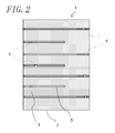
- Fig. 2 is a sectional view of the multi-layer piezoelectric element shown in Fig. 1 taken along a section parallel to a stacked direction of a stacked body, illustrating a part including internal electrode layers each having an exposed end face.
- the multi-layer piezoelectric element 1 of this embodiment comprises a stacked body 7 in which piezoelectric layers 3 and internal electrode layers 5 are alternately laminated in such a way that an end face of each of the internal electrode layers 5 is partly exposed at a side face of the stacked body 7.
- external electrodes 8 taken as a pair, are bonded to the side faces, respectively, of the stacked body 7 so as to make connection with the internal electrode layers 5.
- the end face of each of the internal electrode layers partly exposed at the side face of the stacked body 7 is substantially free from the voids 4.
- the piezoelectric layer 3 constituting the stacked body 7 is made of piezoelectric ceramics having piezoelectric characteristics such for example as a perovskite-type oxide of PbZrO 3 -PbTiO 3 (PZT: lead zirconate titanate).
- the internal electrode layers 5 are alternately laminated together with the piezoelectric layers 3 in such a way that the piezoelectric layer 3 is sandwiched between upper and lower internal electrode layers 5.
- positive electrodes and negative electrodes are arranged in an orderly sequence in the stacked direction, so that a driving voltage can be applied to the piezoelectric layer 3 sandwiched between the electrodes.
- the internal electrode layer 5 is made of a metal such for example as silver-palladium (Ag-Pd).
- positive electrodes and negative electrodes (or grounding electrodes) are led out to the opposed side faces, respectively, of the stacked body 7 in a staggered arrangement, with their end faces partly exposed for electrical connection with the paired external electrodes 8 each bonded to the side face of the stacked body 7.
- a portion between the piezoelectric layers 3 of the stacked body 7 partially has the stress relaxing layer (not shown) instead of the internal electrode layer 5.
- the stress relaxing layer has a strength lower than that of the internal electrode layer 5 and is easily cracked by stress.
- stress generated in the stacked body 7 by driving operation causes damage such as cracks forming sooner in the stress relaxing layer than in the internal electrode layer 5. That is to say, the stress relaxing layers function as stress relaxing layers in the stacked body 7.
- the voids 4 exist in the internal electrode layer 5, and the end face of each of the internal electrode layers 5 partly exposed at the side face of the stacked body 7 is substantially free from the voids 4 (the voids are not observed), and the voids 4 are not exposed at the end face of each of the internal electrode layers 5.
- the multi-layer piezoelectric element 1 is able to extend straight even under a condition of long-time use, and is thus resistant to heat liberation.
- the piezoelectric layer 3 Since the piezoelectric layer 3, whose displacement is temperature-dependent, is not heated, it follows that the multi-layer piezoelectric element 1 can be driven to operate with stability. Moreover, since the voids 4 are substantially nonexistent and are thus not exposed at the exposed end face of each of the internal electrode layers 5, it is possible to protect the exposed end face of each of the internal electrode layers 5 against adsorption of the content of moisture and impurities, and thereby prevent occurrence of migration of metal components between the internal electrode layers 5. Further, since a multiplicity of voids 4 exists in the internal electrode layers 5, it is possible to effectively relax a stress which is applied to the internal electrode layer 5 in the course of driving operation.
- a multiplicity of voids 4 existing in the internal electrode layers 5 ranges in size from 0.1 ⁇ m to 5 ⁇ m in diameter for example, and are scattered overall at a porosity in a range of 5% to 40%.
- porosity refers to the proportion in area of the voids 4 in the cross section of the internal electrode layer 5 in a direction perpendicular to the stacked direction. The porosity of the interior of the internal electrode layer 5 can be adjusted to a desired level in accordance with the following production technique.
- substances that disappear or are released during firing for example, resin powder such as acrylic beads or carbon powder, are admixed in an internal electrode layer conductive paste that is shaped into the internal electrode layer 5. This allows formation of the internal electrode layer 5 in which a multiplicity of voids 4 exists at a desired porosity.
- the end face of each of the internal electrode layers 5 exposed at the side face of the stacked body 7 is flattened by grinding. This makes it possible to ensure that the end face of each of the internal electrode layers 5 exposed at the side face of the stacked body 7 is substantially free from the voids 4. In addition, since the end face has an even surface after the flattening operation, it is possible to achieve uniform concentration of the electric field from the end face of each of the internal electrode layers 5 to the outer side, and thereby prevent occurrence of electrical discharge due to localized concentration of the electric field.
- the surface flattening operation by grinding for the end face of each of the internal electrode layers 5 is carried out as follows.
- the first step is to perform grinding on the end face of each of the internal electrode layers 5 exposed at the side face of the stacked body 7 in a direction parallel to the internal electrode layer 5. After that, the surface of the end face is ground, with the depth of cut set at a low (or zero). In this way, the end face of each of the internal electrode layers 5, being higher in softness than the piezoelectric layer 3, is abrasively machined by an abrasive stone, thereby causing that part of the end face which is exposed at the side face of the stacked body 7 to become deformed so as to fill in the voids 4.
- the stacked body 7 with the internal electrode layer 5 having a flattened end face which is exposed at the side face of the stacked body 7 and is substantially free from the voids 4.
- the expression "the exposed end face of each of the internal electrode layers 5 is substantially free from the voids 4" refers to the condition that, when the end face of each of the internal electrode layers 5 is observed by a metallurgical microscope or SEM (scanning-type microscope), between crystalline particles constituting the internal electrode layer 5 is found a difference in level greater than the diameter of a crystalline particle resulting from the grinding, yet it is recognized that there exists no pore through which a crystalline particle lying inside the crystalline particles constituting the end part of the internal electrode layer 5 can be observed.
- a pore through which the inlying crystalline particle can be observed is defined as the void, whereas a pore through which no inlying crystalline particle is observed is not construed as the void.
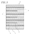
- Fig. 3 is a sectional view of the multi-layer piezoelectric element 1 shown in Fig. 1 taken along a section parallel to the stacked direction of the stacked body 7, illustrating a part including the internal electrode layers 5 having an exposed end face.
- the end part of the internal electrode layer 5 exposed at the side face of the stacked body 7 should preferably be so shaped as to spread over side faces of, respectively, an upper piezoelectric layer 3 and a lower piezoelectric layer 3.
- the end part of each of the internal electrode layers 5 is so shaped as to spread over the side faces of the upper and lower piezoelectric layers 3 on the side face of the stacked body 7, the end part has a so-called nail-headed cross-sectional configuration. This makes it possible to restrain development of a gap between the internal electrode layer 5 and the piezoelectric layer 3 on the side face of the stacked body 7, and thereby provide excellent sealability for the side face of the stacked body 7 where the end face of each of the internal electrode layers 5 is exposed, as is desirable.
- the end part of each of the internal electrode layers 5 spreading over the side faces of the upper and lower piezoelectric layers 3 can be formed as follows.
- the first step is to perform selective grinding in a manner that the piezoelectric layer 3 is ground as appropriate, whereas the internal electrode layer 5 is ground little. Specifically, grinding is performed on the side face of the stacked body 7 in a direction parallel to the internal electrode layer 5 by a wire saw using flowable abrasive grains. In this way, the stacked body 7 can be processed into a form in which the end part of the internal electrode layer 5 protrudes from the side face of the piezoelectric layer 3.
- the side face of the stacked body 7 is abrasively machined in the direction parallel to the internal electrode layer 5 for a plurality of times (preferably three or more times) by a surface grinder or polygon processing machine.
- the depth of cut for the honing is set at a low, preferably 50 ⁇ m or less, more preferably 5 ⁇ m or less.
- piezoelectric ceramic green sheets for constituting the piezoelectric layers 3 are produced. Specifically, calcined powder of piezoelectric ceramics, a binder made of an organic high polymer such as acrylic polymer or butyral polymer, and a plasticizer are mixed to prepare a ceramic slurry. The ceramic slurry is shaped into piezoelectric ceramic green sheets by a tape casting method such as the doctor blade method or the calender roll method.
- the piezoelectric ceramics may be of any given type so long as it has piezoelectric property. For example, a perovskite-type oxide made of lead zirconate titanate (PZT: PbZrO 3 -PbTiO 3 ) can be used.
- a plasticizer dibutyl phthalate (DBP), dioctyl phthalate (DOP), or the like can be used.
- the internal electrode layer conductive paste that is shaped into the internal electrode layer 5 is produced.
- the internal electrode layer conductive paste is prepared by admixing a binder and a plasticizer in metal powder of, for example, a silver-palladium (Ag-Pd) alloy. Note that a mixture of silver powder and palladium powder may be used instead of the silver-palladium alloy.
- the internal electrode layer conductive paste is applied, in a specific pattern of the internal electrode layer 5, onto the piezoelectric ceramic green sheets by means of screen printing, for example.
- a stress relaxing layer paste is applied, in a specific pattern of the stress relaxing layer, onto other piezoelectric ceramic green sheets by means of screen printing.
- the pattern of the stress relaxing layer may be designed either as a whole pattern extending over the range of the entire cross section of the stacked body 7 perpendicular to the stacked direction, or as a partial pattern.
- the paste is printed in a partial pattern with a non-formed region where the stress relaxing layer is not formed, rather than a whole pattern.
- a predetermined number of the piezoelectric ceramic green sheets with coatings of the internal electrode layer conductive paste are laminated on top of each other.
- the piezoelectric ceramic green sheets with coatings of the stress relaxing layer paste are laminated at predetermined spacing (intervals of a predetermined number of the piezoelectric ceramic green sheets).
- firing is performed at 900°C to 1200°C to form a stacked body 7 in which piezoelectric layers 3 and internal electrode layers 5 are alternately laminated and a stress relaxing layer is disposed at part of the portions between the piezoelectric layers 3.
- the side face of the stacked body 7 obtained by firing is abrasively machined to ensure that the end face of each of the internal electrode layers 5 exposed at the side face is substantially free from the voids 4.
- the side face of the stacked body 7, at which is exposed the end face of each of the internal electrode layers 5, is ground in the direction parallel to the internal electrode layer 5 until the stacked body 7 is turned into a predetermined shape by a surface grinder or polygon processing machine using abrasive stones ranging in count from #200 to #1000, for example.
- the side face is further abrasively machined for a plurality of times (preferably three or more times).
- a plurality of times preferably three or more times.
- the end part of each of the internal electrode layers 5 exposed at the side face of the stacked body 7 is shaped so as to spread over the side faces of the upper and lower piezoelectric layers 3 in the following manner. That is, the stacked body 7 obtained by firing is subjected to selective grinding so that the piezoelectric layer 3 is ground as appropriate, whereas the internal electrode layer 5 is ground little. Specifically, the side face of the stacked body 7 is ground in the direction parallel to the internal electrode layer 5 by a wire saw using flowable abrasive grains. In this way, the stacked body 7 can be processed into a form in which the end part of the internal electrode layer 5 protrudes from the side face of the piezoelectric layer 3.
- the side face of the stacked body 7 is abrasively machined in the direction parallel to the internal electrode layer 5 for a plurality of times (preferably three or more times) by a surface grinder or polygon processing machine.
- the depth of cut for the honing is set at a low, preferably 50 ⁇ m or less, more preferably 5 ⁇ m or less.
- a silver-glass conductive paste which is composed predominantly of silver and contains glass is printed, in a specific pattern of the external electrode 8, onto the side face of the stacked body 7 where the internal electrode layer 5 is led out. Then, baking treatment is performed thereon at a temperature in a range of 650°C to 750°C. In this way, the external electrode 8 is formed.
- an external lead member 9 is fixedly connected to the surface of the external electrode 8 via a conductive bonding material (solder) 10.
- the multi-layer piezoelectric element 1 is completed.
- the external electrode 8 and an external power source are connected to each other via the external lead member 9, so that a driving voltage can be applied to the piezoelectric layer 3 via the internal electrode layers 5.
- a driving voltage can be applied to the piezoelectric layer 3 via the internal electrode layers 5.
- the multi-layer piezoelectric element is capable of functioning as, for example, an automotive fuel injection valve for the injection supply of fuel to an engine.
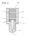
- FIG. 4 is a schematic cross-sectional view showing an example of an injection device according to an embodiment of the invention.
- an injection device 19 of this example comprises a housing (container) 23 comprising an injection hole 21 at one end thereof, and the foregoing multi-layer piezoelectric element 1 of the example placed within the housing 23.
- a needle valve 25 capable of opening and closing of the injection hole 21.
- a fluid passage 27 is so disposed as to be capable of communicating with the injection hole 21 in accordance with the movement of the needle valve 25.
- the fluid passage 27 is coupled to an external fluid supply source, so that a fluid is supplied to the fluid passage 27 under high pressure at all times. Therefore, when the needle valve 25 is operated to open the injection hole 21, then a fluid which has been fed through the fluid passage 27 is injected, through the injection hole 21, to an exterior of the device or into an adjacent container, for example, a fuel chamber of an internal-combustion engine (not shown).
- an upper end of the needle valve 25 is a piston 31 having an inner diameter larger than that of the other portions, and this piston 31 slides along the inner wall 29 of the cylindrical housing 23. Furthermore, the foregoing multi-layer piezoelectric element 1 of the invention is placed within the housing 23.
- the piston 31 upon extension of the multi-layer piezoelectric element 1 entailed by application of voltage, the piston 31 is pushed forward, thus causing the needle valve 25 to close the fluid passage 27 communicating with the injection hole 21 with a consequent halt on supply of fluid. Moreover, upon stopping the application of voltage, the multi-layer piezoelectric element 1 is contracted, and a disc spring 33 pushes the piston 31 backward, thereby opening the fluid passage 27. In consequence, the injection hole 21 communicates with the fluid passage 27 so that injection of fluid can be carried out through the injection hole 21.
- the injection device may be so designed that the fluid passage 27 is opened by applying a voltage to the multi-layer piezoelectric element 1, and is contrariwise closed upon a halt on the application of voltage.
- the injection device of the example may comprise a container 23 comprising an injection hole 21 and the multi-layer piezoelectric element 1 according to the example, wherein a fluid stored in the container is configured to be injected through the injection hole by driving the multi-layer piezoelectric element 1. That is, the multi-layer piezoelectric element 1 does not necessarily have to be placed within the housing 23. It is essential only that a pressure for control of fluid injection is applied to the interior of the housing by driving the multi-layer piezoelectric element 1.
- the term "fluid" is construed as encompassing not only fuel and ink, but also various liquid fluid such as a conductive paste, and gases. The use of the injection device 19 of the example makes it possible to control a flow rate of fluid and timing of fluid injection with stability for a long period of time.
- fuel can be injected toward a combustion chamber of the internal-combustion engine such as an engine with higher accuracy for a longer period of time compared to the case of using a conventional injection device.
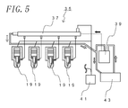
- FIG. 5 is a schematic view showing an example of a fuel injection system according to an embodiment of the invention.
- the fuel injection system 35 of the example comprises a common rail 37 configured to store a high-pressure fuel as a high-pressure fluid, a plurality of the injection devices 19 of the example configured to inject the high-pressure fluid stored in the common rail 37, a pressure pump 39 configured to supply the high-pressure fluid to the common rail 37, and an injection control unit 41 configured to send a drive signal to the injection devices 19.
- the injection control unit 41 controls an amount of injection of the high-pressure fluid and timing of fluid injection on the basis of external information or external signals. For example, in the case of using the fuel injection system 35 for injection of fuel into an engine, it is possible to control the amount of fuel injection and the timing of fuel injection while detecting the condition of the interior of the combustion chamber of the engine by a sensor or the like.
- the pressure pump 39 plays a role of supplying a fluid fuel from a fuel tank 43 to the common rail 37 under high pressure.
- the fluid fuel is fed to the common rail 37 under high pressure of about 1000 to 2000 atmospheres (about 101 MPa to about 203 MPa), and preferably high pressure of about 1500 to 1700 atmospheres (about 152 MPa to about 172 MPa).
- the common rail 37 stores therein the high-pressure fuel from the pressure pump 39 and acts to feed it to the injection device 19 on an as needed basis.
- the injection device 19 injects fluid in a certain amount to the exterior of the device or into an adjacent container through the injection hole 21.
- high-pressure fuel in fine-spray form is injected into the combustion chamber of the engine through the injection hole 21.
- two external electrodes 8 in the multi-layer piezoelectric element 1 are respectively formed on two opposing side faces of the stacked body 7 in the above-described example, two external electrodes 8 may be formed on adjacent side faces of the stacked body 7 or may be formed on the same side face of the stacked body 7.
- the stacked body 7 has a rectangular sectional profile as viewed in a direction perpendicular to the stacked direction
- the sectional profile may be defined by a polygon such as a hexagon or octagon, a circle, or a combination of a straight line and an arc, instead.
- the multi-layer piezoelectric element 1 of the example is used for a piezoelectric driving element (piezoelectric actuator), a pressure sensor element, a piezoelectric circuit element, and so forth.
- the driving element include a fuel injection device for an automotive engine, a liquid injection device such as an ink-jet system, a precise positioning device such as an optical device, and an anti-vibration device.
- the sensor element include a combustion pressure sensor, a knocking sensor, an acceleration sensor, a load sensor, an ultrasound sensor, a pressure-sensing element, and a yaw-rate sensor.
- the circuit element include a piezoelectric gyroscope, a piezoelectric switch, a piezoelectric transformer, and a piezoelectric breaker.
- a piezoelectric actuator comprising the multi-layer piezoelectric element of the invention was fabricated as follows. Firstly, a ceramic slurry was prepared by mixing calcined powder of piezoelectric ceramics composed predominantly of lead zirconate titanate (PZT: PbZrO 3 -PbTiO 3 ) having an average particle size of 0.4 ⁇ m, a binder, and a plasticizer. The ceramic slurry was shaped into piezoelectric ceramic green sheets having a thickness of 100 ⁇ m for forming piezoelectric layers by the doctor blade method. After that, an internal electrode layer conductive paste was prepared by adding a plasticizer and a binder to a mixture composed of silver-palladium alloy powder blended with acrylic beads in an amount of 20% by mass relative to the sum total of the silver-palladium alloy.
- PZT lead zirconate titanate
- the internal electrode layer conductive paste was applied onto the piezoelectric ceramic green sheets by means of screen printing, and 300 pieces of these sheets were laminated on top of each other.
- the resultant was fired at a temperature in a range of 980°C to 1100°C, whereupon a stacked body was obtained.
- the stacked body obtained by firing was ground into a predetermined shape by an abrasive stone with a count of #600, with the depth of cut set at 100 ⁇ m. Then, the side face of the stacked body was abrasively machined 10 times, with the depth of cut changed to 0 ⁇ m.
- the side face of the stacked body in finished form was polished to a mirror-smooth state, and then the internal electrode layer, part of which is exposed at the side face of the stacked body, was examined to check the presence or absence of voids.
- the result showed that a multiplicity of voids, the average size of which was 3 ⁇ m, were substantially evenly distributed inside the internal electrode layer in a proportion of 20% by volume on average, but no voids were observed in the end part of the internal electrode layer exposed at the side face of the stacked body.
- the exposed end face of each of the internal electrode layers was flattened as the result of grinding.
- a silver-glass paste prepared by adding glass, a binder, and a plasticizer to silver powder was printed, in a specific pattern of the external electrode, onto the side face of the stacked body, followed by baking treatment at 700°C. In this way, there was formed the external electrode connected to the internal electrode layer. Then, as an external lead member, a lead wire was fixedly connected to the external electrode with use of solder as a conductive bonding material.
- the example of the multi-layer piezoelectric element of the invention (Sample number 1) was fabricated.
- polarizing treatment on the piezoelectric layers was performed in which a direct-current electric field of 3 kV/mm was applied for 15 minutes via the outer lead members to the external electrodes of the multi-layer piezoelectric elements of Sample numbers 1 and 2.
- the external electrode peels off the stacked body that resulted in sparking, and eventually the operation of the multi-layer piezoelectric element is interrupted.
Landscapes
- Engineering & Computer Science (AREA)
- Chemical & Material Sciences (AREA)
- Combustion & Propulsion (AREA)
- Mechanical Engineering (AREA)
- General Engineering & Computer Science (AREA)
- Manufacturing & Machinery (AREA)
- Fuel-Injection Apparatus (AREA)
Abstract
Description
- The present invention relates to a multi-layer piezoelectric element that can be used as, for example, a piezoelectric driving element (piezoelectric actuator), a pressure sensor element, and a piezoelectric circuit element.
- A conventional multi-layer piezoelectric element has, for example, a stacked body in which piezoelectric layers and internal electrode layers are alternately laminated; and a pair of external electrodes which are bonded to side faces of the stacked body so as to make electrical connection with the internal electrode layers that are set so as to have alternately opposite polarities and are led out to the side faces.
- In such a multi-layer piezoelectric element, in the interest of increased displacement, it has been customary to design the internal electrode layer so that it is exposed at an end face of the stacked body. Meanwhile, Inside the internal electrode layer generally, voids are included, and the voids are uniformly distributed within a plane of the internal electrode layer.
- Besides, the multi-layer piezoelectric element has been required to be adaptable to driving operation at even higher frequencies.
-
- Patent Literature 1: Japanese Unexamined Patent Publication
JP-A 2006-518934 - At the time of driving the multi-layer piezoelectric element, an electric field in the internal electrode layer passes along voids existing within the internal electrode layer, wherefore heat tends to be liberated around the voids. Furthermore, in a part of the internal electrode layer more distant from the external electrode, the higher is the frequency of a drive signal, the larger is a lag in the time of energization. Therefore, the driving timing within the plane of the internal electrode layer may be disturbed in the case of high-speed driving operation at a high-frequency pulse. In consequence, during long-time driving operation, the multi-layer piezoelectric element fails to extend straight, and also there arises decline in the amount of displacement due to heat liberated by the multi-layer piezoelectric element.
- In addition, in the end face of the internal electrode layer exposed at the side face of the stacked body, the content of moisture trapped in the voids existing in the end face caused migration of metal components constituting the internal electrode layer along the end face of the piezoelectric layer.
- This resulted in the difficulty in driving the multi-layer piezoelectric element for a long period of time with stability.
- The invention has been devised in view of the problems associated with the conventional art as mentioned supra, and accordingly an object of the invention is to provide a multi-layer piezoelectric element capable of long-time stable and satisfactory driving operation, in which there is no decline in the amount of displacement even under a condition of long-time use, and an end face of an internal electrode layer lying at a side face of a stacked body can be protected against adsorption of the content of moisture and impurities, thereby preventing occurrence of short-circuiting between the internal electrode layers at the side face of the stacked body.
- The invention provides a multi-layer piezoelectric element, comprising: a stacked body in which piezoelectric layers and internal electrode layers are alternately laminated in such a way that an end face of each of the internal electrode layers is partly exposed at a side face of the stacked body; and a pair of external electrodes that are bonded to side faces of the stacked body so as to make connection with the internal electrode layers, wherein a multiplicity of voids exists in the internal electrode layers, and the end face of each of the internal electrode layers partly exposed at the side face of the stacked body is substantially free from the voids.
- Moreover, in the multi-layer piezoelectric element of the invention, it is preferable that the end face of each of the internal electrode layers exposed at the side face of the stacked body is flattened by grinding.
- Moreover, in the multi-layer piezoelectric element of the invention, it is preferable that an end part of each of the internal electrode layers exposed at the side face of the stacked body is so shaped as to spread over side faces of an upper piezoelectric layer and a lower piezoelectric layer.
- Moreover, the invention provides an injection device, comprising: a container comprising an injection hole; and the multi-layer piezoelectric element mentioned above, wherein a fluid stored in the container is configured to be injected through the injection hole by driving the multi-layer piezoelectric element.
- Moreover the invention provides a fuel injection system, comprising: a common rail configured to store a high-pressure fuel; the injection device mentioned above, configured to inject the high-pressure fuel stored in the common rail; a pressure pump configured to supply the high-pressure fuel to the common rail; and an injection control unit configured to send a drive signal to the injection device.
- According to the multi-layer piezoelectric element of the invention, a multiplicity of voids exists in the internal electrode layers, and the end face of each of the internal electrode layers partly exposed at the side face of the stacked body is substantially free from the voids. That is, since the voids located toward the end face are fewer in number than those located in the inside, it follows that, in the internal electrode layer, an electric field is firstly applied to its periphery (end face), and is whereafter applied to its interior. Therefore, energizations of the individual internal electrode layers at their periphery sides (end-face sides) are timed with one another, which results in coincidences of driving timing within the planes of the individual internal electrode layers. Accordingly, the multi-layer piezoelectric element is able to extend straight even under a condition of long-time use, and is thus resistant to heat liberation. This makes it possible to avoid decline in the amount of displacement.
- Moreover, since the end face of each of the internal electrode layers partly exposed at the side face of the stacked body is substantially free from the voids, it is possible to protect the end face of each of the internal electrode layers against adsorption of the content of moisture and impurities, and thereby prevent occurrence of short-circuiting between the internal electrode layers at the side face of the stacked body. Further, since voids exist in the internal electrode layer, it is possible to reduce a stress applied to the internal electrode layer by virtue of the voids, and thereby drive the multi-layer piezoelectric element satisfactorily for a longer period of time with stability, with consequent enhancement of durability.
- According to the invention, the injection device comprises: the container comprising an injection hole; and the multi-layer piezoelectric element of the invention, wherein a fluid filled in the container is configured to be injected through the injection hole by driving the multi-layer piezoelectric element. Since the highly durable multi-layer piezoelectric element of the invention is used, the injection device succeeds in providing excellent durability.
- According to the invention, the fuel injection system comprises: the common rail configured to store a high-pressure fuel; the injection device of the invention configured to inject the high-pressure fuel stored in the common rail; the pressure pump configured to supply the high-pressure fuel to the common rail; and the injection control unit configured to send a drive signal to the injection device. Since the injection device of the invention incorporating the highly durable multi-layer piezoelectric element of the invention is used, the fuel injection system succeeds in providing excellent durability.
-
-
Fig. 1 is a perspective view showing an example of a multi-layer piezoelectric element according to an embodiment of the invention; -
Fig. 2 is a sectional view of the multi-layer piezoelectric element shown inFig. 1 taken along a section parallel to a stacked direction of a stacked body, illustrating a part including internal electrode layers each having an exposed end face; -
Fig. 3 is a sectional view of the multi-layer piezoelectric element shown inFig. 1 taken along a section parallel to the stacked direction of the stacked body, illustrating a part including the internal electrode layers having an exposed end face; -
Fig. 4 is a schematic sectional view showing an example of an injection device according to an embodiment of the invention; and -
Fig. 5 is a schematic block diagram showing an example of a fuel injection system according to an embodiment of the invention. - Hereinafter, examples of a multi-layer piezoelectric element according to an embodiment of the invention will be described in detail with reference to the drawings.
-
Fig. 1 is a perspective view showing an example of a multi-layer piezoelectric element according to an embodiment of the invention.Fig. 2 is a sectional view of the multi-layer piezoelectric element shown inFig. 1 taken along a section parallel to a stacked direction of a stacked body, illustrating a part including internal electrode layers each having an exposed end face. As shown inFigs. 1 and2 , the multi-layerpiezoelectric element 1 of this embodiment comprises astacked body 7 in whichpiezoelectric layers 3 andinternal electrode layers 5 are alternately laminated in such a way that an end face of each of theinternal electrode layers 5 is partly exposed at a side face of thestacked body 7. Moreover,external electrodes 8, taken as a pair, are bonded to the side faces, respectively, of thestacked body 7 so as to make connection with theinternal electrode layers 5. At this time, while a multiplicity ofvoids 4 exists in theinternal electrode layers 5, the end face of each of the internal electrode layers partly exposed at the side face of thestacked body 7 is substantially free from thevoids 4. - The
piezoelectric layer 3 constituting the stackedbody 7 is made of piezoelectric ceramics having piezoelectric characteristics such for example as a perovskite-type oxide of PbZrO3-PbTiO3 (PZT: lead zirconate titanate). Moreover, theinternal electrode layers 5 are alternately laminated together with thepiezoelectric layers 3 in such a way that thepiezoelectric layer 3 is sandwiched between upper and lowerinternal electrode layers 5. In this way, positive electrodes and negative electrodes are arranged in an orderly sequence in the stacked direction, so that a driving voltage can be applied to thepiezoelectric layer 3 sandwiched between the electrodes. Theinternal electrode layer 5 is made of a metal such for example as silver-palladium (Ag-Pd). In this embodiment, positive electrodes and negative electrodes (or grounding electrodes) are led out to the opposed side faces, respectively, of thestacked body 7 in a staggered arrangement, with their end faces partly exposed for electrical connection with the pairedexternal electrodes 8 each bonded to the side face of thestacked body 7. - Furthermore, a portion between the
piezoelectric layers 3 of thestacked body 7 partially has the stress relaxing layer (not shown) instead of theinternal electrode layer 5. The stress relaxing layer has a strength lower than that of theinternal electrode layer 5 and is easily cracked by stress. Thus, stress generated in the stackedbody 7 by driving operation causes damage such as cracks forming sooner in the stress relaxing layer than in theinternal electrode layer 5. That is to say, the stress relaxing layers function as stress relaxing layers in thestacked body 7. - In the multi-layer
piezoelectric element 1 of the invention, as shown inFig. 2 , thevoids 4 exist in theinternal electrode layer 5, and the end face of each of theinternal electrode layers 5 partly exposed at the side face of thestacked body 7 is substantially free from the voids 4 (the voids are not observed), and thevoids 4 are not exposed at the end face of each of theinternal electrode layers 5. - In the case where the
voids 4 are not exposed at the end face of each of theinternal electrode layers 5 exposed at the side face of thestacked body 7, expressed differently, are substantially nonexistent (not observed), in theinternal electrode layer 5, an electric field induced by the driving voltage applied to theinternal electrode layer 5 through theexternal electrode 8 is firstly applied to its periphery (end face), and is whereafter applied to its interior. Therefore, energizations of the individualinternal electrode layers 5 at their periphery sides (end-face sides) are timed with one another, which results in coincidences of driving timing within the planes of the individualinternal electrode layers 5. Accordingly, the multi-layerpiezoelectric element 1 is able to extend straight even under a condition of long-time use, and is thus resistant to heat liberation. Since thepiezoelectric layer 3, whose displacement is temperature-dependent, is not heated, it follows that the multi-layerpiezoelectric element 1 can be driven to operate with stability. Moreover, since thevoids 4 are substantially nonexistent and are thus not exposed at the exposed end face of each of theinternal electrode layers 5, it is possible to protect the exposed end face of each of theinternal electrode layers 5 against adsorption of the content of moisture and impurities, and thereby prevent occurrence of migration of metal components between theinternal electrode layers 5. Further, since a multiplicity ofvoids 4 exists in theinternal electrode layers 5, it is possible to effectively relax a stress which is applied to theinternal electrode layer 5 in the course of driving operation. - In the interior of the
stacked body 7, a multiplicity ofvoids 4 existing in theinternal electrode layers 5 ranges in size from 0.1 µm to 5 µm in diameter for example, and are scattered overall at a porosity in a range of 5% to 40%. As used herein, the term "porosity" refers to the proportion in area of thevoids 4 in the cross section of theinternal electrode layer 5 in a direction perpendicular to the stacked direction. The porosity of the interior of theinternal electrode layer 5 can be adjusted to a desired level in accordance with the following production technique. Specifically, substances that disappear or are released during firing, for example, resin powder such as acrylic beads or carbon powder, are admixed in an internal electrode layer conductive paste that is shaped into theinternal electrode layer 5. This allows formation of theinternal electrode layer 5 in which a multiplicity ofvoids 4 exists at a desired porosity. - In the multi-layer
piezoelectric element 1 of the invention, it is preferable that the end face of each of theinternal electrode layers 5 exposed at the side face of thestacked body 7 is flattened by grinding. This makes it possible to ensure that the end face of each of theinternal electrode layers 5 exposed at the side face of thestacked body 7 is substantially free from thevoids 4. In addition, since the end face has an even surface after the flattening operation, it is possible to achieve uniform concentration of the electric field from the end face of each of theinternal electrode layers 5 to the outer side, and thereby prevent occurrence of electrical discharge due to localized concentration of the electric field. - The surface flattening operation by grinding for the end face of each of the
internal electrode layers 5 is carried out as follows. The first step is to perform grinding on the end face of each of theinternal electrode layers 5 exposed at the side face of thestacked body 7 in a direction parallel to theinternal electrode layer 5. After that, the surface of the end face is ground, with the depth of cut set at a low (or zero). In this way, the end face of each of theinternal electrode layers 5, being higher in softness than thepiezoelectric layer 3, is abrasively machined by an abrasive stone, thereby causing that part of the end face which is exposed at the side face of thestacked body 7 to become deformed so as to fill in thevoids 4. As a result, there is obtained thestacked body 7 with theinternal electrode layer 5 having a flattened end face which is exposed at the side face of thestacked body 7 and is substantially free from thevoids 4. As used herein, the expression "the exposed end face of each of theinternal electrode layers 5 is substantially free from thevoids 4" refers to the condition that, when the end face of each of theinternal electrode layers 5 is observed by a metallurgical microscope or SEM (scanning-type microscope), between crystalline particles constituting theinternal electrode layer 5 is found a difference in level greater than the diameter of a crystalline particle resulting from the grinding, yet it is recognized that there exists no pore through which a crystalline particle lying inside the crystalline particles constituting the end part of theinternal electrode layer 5 can be observed. In other words, a pore through which the inlying crystalline particle can be observed is defined as the void, whereas a pore through which no inlying crystalline particle is observed is not construed as the void. - Next,
Fig. 3 is a sectional view of the multi-layerpiezoelectric element 1 shown inFig. 1 taken along a section parallel to the stacked direction of thestacked body 7, illustrating a part including theinternal electrode layers 5 having an exposed end face. In the multi-layerpiezoelectric element 1 of the invention, as shown inFig. 3 , the end part of theinternal electrode layer 5 exposed at the side face of thestacked body 7 should preferably be so shaped as to spread over side faces of, respectively, an upperpiezoelectric layer 3 and a lowerpiezoelectric layer 3. In the case where the end part of each of theinternal electrode layers 5 is so shaped as to spread over the side faces of the upper and lowerpiezoelectric layers 3 on the side face of thestacked body 7, the end part has a so-called nail-headed cross-sectional configuration. This makes it possible to restrain development of a gap between theinternal electrode layer 5 and thepiezoelectric layer 3 on the side face of thestacked body 7, and thereby provide excellent sealability for the side face of thestacked body 7 where the end face of each of theinternal electrode layers 5 is exposed, as is desirable. - The end part of each of the
internal electrode layers 5 spreading over the side faces of the upper and lowerpiezoelectric layers 3 can be formed as follows. The first step is to perform selective grinding in a manner that thepiezoelectric layer 3 is ground as appropriate, whereas theinternal electrode layer 5 is ground little. Specifically, grinding is performed on the side face of thestacked body 7 in a direction parallel to theinternal electrode layer 5 by a wire saw using flowable abrasive grains. In this way, thestacked body 7 can be processed into a form in which the end part of theinternal electrode layer 5 protrudes from the side face of thepiezoelectric layer 3. After that, in the manner as above described, the side face of thestacked body 7 is abrasively machined in the direction parallel to theinternal electrode layer 5 for a plurality of times (preferably three or more times) by a surface grinder or polygon processing machine. At this time, the depth of cut for the honing is set at a low, preferably 50 µm or less, more preferably 5 µm or less. As a result, the end part of each of theinternal electrode layers 5 protruding from the side face of thepiezoelectric layer 3 is crushed from above downward to become deformed so as to spread over the side faces of the upper and lowerpiezoelectric layers 3. - Next, an example of a method for manufacturing the multi-layer
piezoelectric element 1 of this example will be described. - To begin with, piezoelectric ceramic green sheets for constituting the
piezoelectric layers 3 are produced. Specifically, calcined powder of piezoelectric ceramics, a binder made of an organic high polymer such as acrylic polymer or butyral polymer, and a plasticizer are mixed to prepare a ceramic slurry. The ceramic slurry is shaped into piezoelectric ceramic green sheets by a tape casting method such as the doctor blade method or the calender roll method. The piezoelectric ceramics may be of any given type so long as it has piezoelectric property. For example, a perovskite-type oxide made of lead zirconate titanate (PZT: PbZrO3-PbTiO3) can be used. Moreover, as the plasticizer, dibutyl phthalate (DBP), dioctyl phthalate (DOP), or the like can be used. - Then, an internal electrode layer conductive paste that is shaped into the
internal electrode layer 5 is produced. Specifically, the internal electrode layer conductive paste is prepared by admixing a binder and a plasticizer in metal powder of, for example, a silver-palladium (Ag-Pd) alloy. Note that a mixture of silver powder and palladium powder may be used instead of the silver-palladium alloy. - In order to form a multiplicity of
voids 4 in theinternal electrode layers 5 effectively, it is desirable to mix substances that disappear or are released during firing, such for example as acrylic beads, in the internal electrode layer conductive paste. Following the completion of firing, areas of the paste which bore acrylic beads become thevoids 4 that exist in theinternal electrode layer 5. - Then, the internal electrode layer conductive paste is applied, in a specific pattern of the
internal electrode layer 5, onto the piezoelectric ceramic green sheets by means of screen printing, for example. - Moreover, a stress relaxing layer paste is applied, in a specific pattern of the stress relaxing layer, onto other piezoelectric ceramic green sheets by means of screen printing. The pattern of the stress relaxing layer may be designed either as a whole pattern extending over the range of the entire cross section of the
stacked body 7 perpendicular to the stacked direction, or as a partial pattern. Preferably, the paste is printed in a partial pattern with a non-formed region where the stress relaxing layer is not formed, rather than a whole pattern. Moreover, in the interest of preventing occurrence of short-circuiting between the pairedexternal electrodes 8 without fail, it is desirable to adopt a pattern such that the non-formed region acts as partition between the positive and negativeexternal electrodes 8. - Then, a predetermined number of the piezoelectric ceramic green sheets with coatings of the internal electrode layer conductive paste are laminated on top of each other. At this time, the piezoelectric ceramic green sheets with coatings of the stress relaxing layer paste are laminated at predetermined spacing (intervals of a predetermined number of the piezoelectric ceramic green sheets). Moreover, it is possible to laminate a conductive paste-free piezoelectric ceramic green sheet on each of the top and the bottom of the resultant layered body as opposite end parts.
- Furthermore, after debinding treatment at a predetermined temperature, firing is performed at 900°C to 1200°C to form a
stacked body 7 in whichpiezoelectric layers 3 andinternal electrode layers 5 are alternately laminated and a stress relaxing layer is disposed at part of the portions between thepiezoelectric layers 3. - Next, the side face of the
stacked body 7 obtained by firing is abrasively machined to ensure that the end face of each of theinternal electrode layers 5 exposed at the side face is substantially free from thevoids 4. Specifically, the side face of thestacked body 7, at which is exposed the end face of each of theinternal electrode layers 5, is ground in the direction parallel to theinternal electrode layer 5 until thestacked body 7 is turned into a predetermined shape by a surface grinder or polygon processing machine using abrasive stones ranging in count from #200 to #1000, for example. Then, after the depth of cut is reduced to a low, preferably 50 µm or below, more preferably 5 µm or below, the side face is further abrasively machined for a plurality of times (preferably three or more times). Thereby, only theinternal electrode layer 5 which is softer than thepiezoelectric layer 3 is plastically, or ductilly deformed by the honing so as to fill in thevoid 4 exposed at the end face. This makes it possible to ensure that the end face of each of theinternal electrode layers 5 exposed at the side face of thestacked body 7 is substantially free from thevoids 4. - Further, as shown in
Fig. 3 , the end part of each of theinternal electrode layers 5 exposed at the side face of thestacked body 7 is shaped so as to spread over the side faces of the upper and lowerpiezoelectric layers 3 in the following manner. That is, thestacked body 7 obtained by firing is subjected to selective grinding so that thepiezoelectric layer 3 is ground as appropriate, whereas theinternal electrode layer 5 is ground little. Specifically, the side face of thestacked body 7 is ground in the direction parallel to theinternal electrode layer 5 by a wire saw using flowable abrasive grains. In this way, thestacked body 7 can be processed into a form in which the end part of theinternal electrode layer 5 protrudes from the side face of thepiezoelectric layer 3. After that, in the manner as above described, the side face of thestacked body 7 is abrasively machined in the direction parallel to theinternal electrode layer 5 for a plurality of times (preferably three or more times) by a surface grinder or polygon processing machine. At this time, the depth of cut for the honing is set at a low, preferably 50 µm or less, more preferably 5 µm or less. As a result, the end part of each of theinternal electrode layers 5 protruding from the side face of thepiezoelectric layer 3 is crushed from above downward so as to spread over the side faces of the upper and lowerpiezoelectric layers 3. - Subsequently, a silver-glass conductive paste which is composed predominantly of silver and contains glass is printed, in a specific pattern of the
external electrode 8, onto the side face of thestacked body 7 where theinternal electrode layer 5 is led out. Then, baking treatment is performed thereon at a temperature in a range of 650°C to 750°C. In this way, theexternal electrode 8 is formed. - Then, an
external lead member 9 is fixedly connected to the surface of theexternal electrode 8 via a conductive bonding material (solder) 10. - After that, a direct-current electric field of 0.1 to 3 kV/mm is applied, through the
external electrodes 8 and theinternal electrode layer 5, to thepiezoelectric layer 3 from theexternal lead member 9 connected to each of the pairedexternal electrodes 8 to initiate polarization in thepiezoelectric layer 3 constituting thestacked body 7. In this way, the construction of the multi-layerpiezoelectric element 1 is completed. In this multi-layerpiezoelectric element 1, theexternal electrode 8 and an external power source are connected to each other via theexternal lead member 9, so that a driving voltage can be applied to thepiezoelectric layer 3 via the internal electrode layers 5. This allows each of thepiezoelectric layers 3 to undergo significant displacement under an inverse piezoelectric effect. Thus, the multi-layer piezoelectric element is capable of functioning as, for example, an automotive fuel injection valve for the injection supply of fuel to an engine. - Next, an example of an injection device according to an embodiment of the invention will be described.
Fig. 4 is a schematic cross-sectional view showing an example of an injection device according to an embodiment of the invention. - As shown in
Fig. 4 , aninjection device 19 of this example comprises a housing (container) 23 comprising aninjection hole 21 at one end thereof, and the foregoing multi-layerpiezoelectric element 1 of the example placed within thehousing 23. - In an interior of the
housing 23 is disposed aneedle valve 25 capable of opening and closing of theinjection hole 21. Afluid passage 27 is so disposed as to be capable of communicating with theinjection hole 21 in accordance with the movement of theneedle valve 25. Thefluid passage 27 is coupled to an external fluid supply source, so that a fluid is supplied to thefluid passage 27 under high pressure at all times. Therefore, when theneedle valve 25 is operated to open theinjection hole 21, then a fluid which has been fed through thefluid passage 27 is injected, through theinjection hole 21, to an exterior of the device or into an adjacent container, for example, a fuel chamber of an internal-combustion engine (not shown). - Furthermore, an upper end of the
needle valve 25 is a piston 31 having an inner diameter larger than that of the other portions, and this piston 31 slides along theinner wall 29 of thecylindrical housing 23. Furthermore, the foregoing multi-layerpiezoelectric element 1 of the invention is placed within thehousing 23. - In the
injection device 19, upon extension of the multi-layerpiezoelectric element 1 entailed by application of voltage, the piston 31 is pushed forward, thus causing theneedle valve 25 to close thefluid passage 27 communicating with theinjection hole 21 with a consequent halt on supply of fluid. Moreover, upon stopping the application of voltage, the multi-layerpiezoelectric element 1 is contracted, and adisc spring 33 pushes the piston 31 backward, thereby opening thefluid passage 27. In consequence, theinjection hole 21 communicates with thefluid passage 27 so that injection of fluid can be carried out through theinjection hole 21. - It is noted that the injection device may be so designed that the
fluid passage 27 is opened by applying a voltage to the multi-layerpiezoelectric element 1, and is contrariwise closed upon a halt on the application of voltage. - Moreover, the injection device of the example may comprise a
container 23 comprising aninjection hole 21 and the multi-layerpiezoelectric element 1 according to the example, wherein a fluid stored in the container is configured to be injected through the injection hole by driving the multi-layerpiezoelectric element 1. That is, the multi-layerpiezoelectric element 1 does not necessarily have to be placed within thehousing 23. It is essential only that a pressure for control of fluid injection is applied to the interior of the housing by driving the multi-layerpiezoelectric element 1. In theinjection device 19 of this example, the term "fluid" is construed as encompassing not only fuel and ink, but also various liquid fluid such as a conductive paste, and gases. The use of theinjection device 19 of the example makes it possible to control a flow rate of fluid and timing of fluid injection with stability for a long period of time. - When the
injection device 19 of this example using the multi-layerpiezoelectric element 1 of this example is used for an internal-combustion engine, fuel can be injected toward a combustion chamber of the internal-combustion engine such as an engine with higher accuracy for a longer period of time compared to the case of using a conventional injection device. - Next, an example of a fuel injection system according to an embodiment of the invention will be described.
Fig. 5 is a schematic view showing an example of a fuel injection system according to an embodiment of the invention. - As shown in
Fig. 5 , thefuel injection system 35 of the example comprises acommon rail 37 configured to store a high-pressure fuel as a high-pressure fluid, a plurality of theinjection devices 19 of the example configured to inject the high-pressure fluid stored in thecommon rail 37, apressure pump 39 configured to supply the high-pressure fluid to thecommon rail 37, and an injection control unit 41 configured to send a drive signal to theinjection devices 19. - The injection control unit 41 controls an amount of injection of the high-pressure fluid and timing of fluid injection on the basis of external information or external signals. For example, in the case of using the
fuel injection system 35 for injection of fuel into an engine, it is possible to control the amount of fuel injection and the timing of fuel injection while detecting the condition of the interior of the combustion chamber of the engine by a sensor or the like. Thepressure pump 39 plays a role of supplying a fluid fuel from a fuel tank 43 to thecommon rail 37 under high pressure. For example, in thefuel injection system 35 for use in engine application, the fluid fuel is fed to thecommon rail 37 under high pressure of about 1000 to 2000 atmospheres (about 101 MPa to about 203 MPa), and preferably high pressure of about 1500 to 1700 atmospheres (about 152 MPa to about 172 MPa). Thecommon rail 37 stores therein the high-pressure fuel from thepressure pump 39 and acts to feed it to theinjection device 19 on an as needed basis. As has already been described, theinjection device 19 injects fluid in a certain amount to the exterior of the device or into an adjacent container through theinjection hole 21. For example, in the case where an engine is a target of fuel supply by injection, high-pressure fuel in fine-spray form is injected into the combustion chamber of the engine through theinjection hole 21. - It is to be understood that the application of the invention is not limited to the specific embodiments described heretofore, and that various changes and modifications can be made without departing from the gist of the invention. For example, although two
external electrodes 8 in the multi-layerpiezoelectric element 1 are respectively formed on two opposing side faces of thestacked body 7 in the above-described example, twoexternal electrodes 8 may be formed on adjacent side faces of thestacked body 7 or may be formed on the same side face of thestacked body 7. Furthermore, while, in the foregoing examples, thestacked body 7 has a rectangular sectional profile as viewed in a direction perpendicular to the stacked direction, the sectional profile may be defined by a polygon such as a hexagon or octagon, a circle, or a combination of a straight line and an arc, instead. - For example, the multi-layer
piezoelectric element 1 of the example is used for a piezoelectric driving element (piezoelectric actuator), a pressure sensor element, a piezoelectric circuit element, and so forth. Examples of the driving element include a fuel injection device for an automotive engine, a liquid injection device such as an ink-jet system, a precise positioning device such as an optical device, and an anti-vibration device. Examples of the sensor element include a combustion pressure sensor, a knocking sensor, an acceleration sensor, a load sensor, an ultrasound sensor, a pressure-sensing element, and a yaw-rate sensor. Examples of the circuit element include a piezoelectric gyroscope, a piezoelectric switch, a piezoelectric transformer, and a piezoelectric breaker. - Hereinafter, an example of the multi-layer piezoelectric element of the invention will be described.
- A piezoelectric actuator comprising the multi-layer piezoelectric element of the invention was fabricated as follows. Firstly, a ceramic slurry was prepared by mixing calcined powder of piezoelectric ceramics composed predominantly of lead zirconate titanate (PZT: PbZrO3-PbTiO3) having an average particle size of 0.4 µm, a binder, and a plasticizer. The ceramic slurry was shaped into piezoelectric ceramic green sheets having a thickness of 100 µm for forming piezoelectric layers by the doctor blade method. After that, an internal electrode layer conductive paste was prepared by adding a plasticizer and a binder to a mixture composed of silver-palladium alloy powder blended with acrylic beads in an amount of 20% by mass relative to the sum total of the silver-palladium alloy.
- Then, the internal electrode layer conductive paste was applied onto the piezoelectric ceramic green sheets by means of screen printing, and 300 pieces of these sheets were laminated on top of each other.
- The resultant was fired at a temperature in a range of 980°C to 1100°C, whereupon a stacked body was obtained.
- Next, the stacked body obtained by firing was ground into a predetermined shape by an abrasive stone with a count of #600, with the depth of cut set at 100 µm. Then, the side face of the stacked body was abrasively machined 10 times, with the depth of cut changed to 0 µm.
- In this way, there was obtained the stacked body in which a multiplicity of voids exists in the internal electrode layers and the end face of each of the internal electrode layer partly exposed at the side face of the stacked body is substantially free from the voids.
- Next, the side face of the stacked body in finished form was polished to a mirror-smooth state, and then the internal electrode layer, part of which is exposed at the side face of the stacked body, was examined to check the presence or absence of voids. The result showed that a multiplicity of voids, the average size of which was 3 µm, were substantially evenly distributed inside the internal electrode layer in a proportion of 20% by volume on average, but no voids were observed in the end part of the internal electrode layer exposed at the side face of the stacked body. At this time, the exposed end face of each of the internal electrode layers was flattened as the result of grinding.
- Subsequently, a silver-glass paste prepared by adding glass, a binder, and a plasticizer to silver powder was printed, in a specific pattern of the external electrode, onto the side face of the stacked body, followed by baking treatment at 700°C. In this way, there was formed the external electrode connected to the internal electrode layer. Then, as an external lead member, a lead wire was fixedly connected to the external electrode with use of solder as a conductive bonding material. In the manner as above described, the example of the multi-layer piezoelectric element of the invention (Sample number 1) was fabricated.
- On the other hand, by way of a comparative example, there was fabricated a sample in which the stacked body obtained by firing was ground into a predetermined shape by an abrasive stone with a count of #600, with the depth of cut set at 100 µm. Likewise, in this sample, the side face of the stacked body was polished to a mirror-smooth state, and then the internal electrode layer, part of which was exposed at the side face of the stacked body, was examined to check the presence or absence of voids. The result showed that a multiplicity of voids, the average size of which was 3 µm, were substantially evenly distributed inside the internal electrode layer in a proportion of 20% by volume on average, and similarly a multiplicity of voids of the same average size was substantially evenly distributed, in a proportion of 20% by volume on average, even in the end part of the internal electrode layer exposed at the side face of the stacked body.
- Subsequently, based on the sample for the comparative example, there was fabricated a stacked body, the side face of which where the end face of each of the internal electrode layers was exposed was abrasively machined by a surface grinder, so that a multiplicity of voids was exposed at the end face of each of the internal electrode layers. The side face of the stacked body thus obtained was then coated with silicone resin. In this way, the comparative example of the multi-layer piezoelectric element (Sample number 2) was fabricated.
- Next, polarizing treatment on the piezoelectric layers was performed in which a direct-current electric field of 3 kV/mm was applied for 15 minutes via the outer lead members to the external electrodes of the multi-layer piezoelectric elements of
Sample numbers 1 and 2. - An alternating-current voltage of 0 V to +160 V was applied to the multi-layer piezoelectric elements of
Sample numbers 1 and 2 in an atmosphere of 150°C and at a frequency of 150 Hz, and a durability test that performed continuous driving opeariton 1 × 10⁸ times was carried out. Table 1 shows the obtained results.Table 1 Sample number Durability test result 1 No problem occurred after 1 × 10^8 cycles of driving operation 2 External electrode peeled off stacked body that resulted in sparking after 2 × 10^7 cycles of driving operation - As shown in
Fig. 1 , in the multi-layer piezoelectric element implemented by way of the example of the invention (Sample number 1), even after 1 × 10⁸ cycles of continuous driving operation, there was no sign of abnormality. This is because, since the exposed end face of each of the internal electrode layers is substantially free from the voids and thus voids located outward are few in number, it followed that, in the internal electrode layer, an electric field is applied firstly to its periphery, and is whereafter applied to its interior for energization. Therefore, energizations of the individual internal electrode layers at their peripheral sides are timed with one another, which resulted in coincidences of driving timing within the planes parallel to the internal electrode layers. As a result, the stacked body is able to extend straight even under a long-time driving operation, and the multi-layer piezoelectric element becomes resistant to heat liberation. This makes it possible to avoid decline in the amount of displacement. - Moreover, since the number of voids in the end face, or the peripheral side of the internal electrode layer is reduced, it becomes possible to protect the end face against adsorption of the content of moisture and impurities, and thereby prevent occurrence of short-circuiting between the internal electrode layers at the side face of the stacked body. Meanwhile, since a multiplicity of voids exists inside the internal electrode layers, a stress applied to the internal electrode layer can be relaxed, with consequent enhancement of durability. Further, since localized concentration of the electric field at part of the end face of each of the internal electrode layers can be restrained for prevention of occurrence of electrical discharge, it becomes possible to provide excellent sealability for the end face of each of the internal electrode layers.
- On the other hand, in the multi-layer piezoelectric element implemented by way of the comparative example (Sample number 2), after 2 × 10⁶ cycles of continuous driving operation, the external electrode peels off the stacked body that resulted in sparking, and eventually the operation of the multi-layer piezoelectric element is interrupted.
-
- 1:
- Multi-layer piezoelectric element
- 3:
- Piezoelectric layer
- 4:
- Void
- 5:
- Internal electrode layer
- 7:
- Stacked body
- 8:
- External electrode
- 9:
- External lead member
- 19:
- Injection device
- 21:
- Injection hole
- 23:
- Housing (Container)
- 25:
- Needle valve
- 27:
- Fluid passage
- 29:
- Cylinder
- 31:
- Piston
- 33:
- Disc spring
- 35:
- Fuel injection system
- 37:
- Common rail
- 39:
- Pressure pump
- 41:
- Injection control unit
- 43:
- Fuel tank
Claims (5)
- A multi-layer piezoelectric element, comprising:a stacked body in which piezoelectric layers and internal electrode layers are alternately laminated in such a way that an end face of each of the internal electrode layers is partly exposed at a side face of the stacked body; anda pair of external electrodes that are bonded to side faces of the stacked body so as to make connection with the internal electrode layers,wherein a multiplicity of voids exists in the internal electrode layers, and the end face of each of the internal electrode layers partly exposed at the side face of the stacked body is substantially free from the voids.
- The multi-layer piezoelectric element according to claim 1, wherein the end face of each of the internal electrode layers exposed at the side face of the stacked body is flattened by grinding.
- The multi-layer piezoelectric element according to claim 1, wherein an end part of each of the internal electrode layers exposed at the side face of the stacked body is so shaped as to spread over side faces of an upper piezoelectric layer and a lower piezoelectric layer.
- An injection device, comprising:a container comprising an injection hole; andthe multi-layer piezoelectric element according to any one of claims 1 to 3, whereina fluid stored in the container is configured to be injected through the injection hole by driving the multi-layer piezoelectric element.
- A fuel injection system, comprising:a common rail configured to store a high-pressure fuel;the injection device according to claim 4, configured to inject the high-pressure fuel stored in the common rail;a pressure pump configured to supply the high-pressure fuel to the common rail; andan injection control unit configured to send a drive signal to the injection device.
Applications Claiming Priority (2)
| Application Number | Priority Date | Filing Date | Title |
|---|---|---|---|
| JP2009196348 | 2009-08-27 | ||
| PCT/JP2010/064590 WO2011024948A1 (en) | 2009-08-27 | 2010-08-27 | Multilayer piezoelectric element, and injection apparatus and fuel injection system using same |
Publications (3)
| Publication Number | Publication Date |
|---|---|
| EP2472620A1 true EP2472620A1 (en) | 2012-07-04 |
| EP2472620A4 EP2472620A4 (en) | 2014-08-27 |
| EP2472620B1 EP2472620B1 (en) | 2018-06-13 |
Family
ID=43628046
Family Applications (1)
| Application Number | Title | Priority Date | Filing Date |
|---|---|---|---|
| EP10811997.5A Active EP2472620B1 (en) | 2009-08-27 | 2010-08-27 | Multilayer piezoelectric element, and injection device and fuel injection device using the same |
Country Status (5)
| Country | Link |
|---|---|
| US (1) | US20120187212A1 (en) |
| EP (1) | EP2472620B1 (en) |
| JP (1) | JP5496210B2 (en) |
| CN (1) | CN102473836A (en) |
| WO (1) | WO2011024948A1 (en) |
Cited By (1)
| Publication number | Priority date | Publication date | Assignee | Title |
|---|---|---|---|---|
| JP2017157830A (en) * | 2016-02-26 | 2017-09-07 | 京セラ株式会社 | Piezoelectric ceramic plate, plate-like substrate, and electronic component |
Families Citing this family (3)
| Publication number | Priority date | Publication date | Assignee | Title |
|---|---|---|---|---|
| US8578911B2 (en) * | 2008-07-29 | 2013-11-12 | Kyocera Corporation | Multi-layer piezoelectric element, and injection device and fuel injection system using the same |
| WO2011096335A1 (en) * | 2010-02-04 | 2011-08-11 | 株式会社 村田製作所 | Process for producing esd protection device, and esd protection device |
| WO2019073783A1 (en) * | 2017-10-12 | 2019-04-18 | 住友電気工業株式会社 | Ceramic substrate, laminate, and saw device |
Citations (6)
| Publication number | Priority date | Publication date | Assignee | Title |
|---|---|---|---|---|
| US5073740A (en) * | 1987-09-25 | 1991-12-17 | Hitachi Metals, Ltd. | Laminate-type displacement element |
| US20040262037A1 (en) * | 2000-02-16 | 2004-12-30 | Taiyo Yuden Co., Ltd. | Multilayer displacement element and method for manufacturing same |
| US20060061237A1 (en) * | 2003-06-06 | 2006-03-23 | Ngk Insulators, Ltd. | Piezoelectric/electrostrictive element, method of manufacturing piezoelectric/electrostrictive element, piezoelectric/electrostrictive device, and method of manufacturing piezoelectric/electrostrictive device |
| US20060145401A1 (en) * | 2003-02-21 | 2006-07-06 | Kenjiro Mihara | Laminate type ceramic electronic components and method of producing the same |
| US20060274042A1 (en) * | 2005-06-03 | 2006-12-07 | Apple Computer, Inc. | Mouse with improved input mechanisms |
| WO2009096381A1 (en) * | 2008-01-29 | 2009-08-06 | Kyocera Corporation | Laminated piezoelectric element, and injector equipped with laminated piezoelectric element and fuel injection system |
Family Cites Families (16)
| Publication number | Priority date | Publication date | Assignee | Title |
|---|---|---|---|---|
| JPH11163426A (en) * | 1997-11-28 | 1999-06-18 | Kyocera Corp | Laminated piezoelectric actuator |
| JP3872349B2 (en) * | 2002-01-24 | 2007-01-24 | 京セラ株式会社 | Manufacturing method of multilayer piezoelectric element |
| JP4165237B2 (en) * | 2003-01-28 | 2008-10-15 | トヨタ自動車株式会社 | Start control device for internal combustion engine |
| JP4635439B2 (en) * | 2003-02-12 | 2011-02-23 | 株式会社デンソー | Multilayer piezoelectric element and method for manufacturing the same |
| DE10307825A1 (en) | 2003-02-24 | 2004-09-09 | Epcos Ag | Electrical multilayer component and layer stack |
| CN100563039C (en) * | 2004-03-09 | 2009-11-25 | 京瓷株式会社 | Laminate type piezoelectric element and manufacture method thereof |
| DE102004038103A1 (en) * | 2004-08-05 | 2006-02-23 | Epcos Ag | Multi-layer component and method for its production |
| JP2006156587A (en) * | 2004-11-26 | 2006-06-15 | Tdk Corp | Multilayer piezoelectric element |
| EP1898476B1 (en) * | 2005-06-15 | 2014-11-19 | Kyocera Corporation | Multilayer piezoelectric element and ejector using this |
| WO2007049456A1 (en) * | 2005-10-28 | 2007-05-03 | Murata Manufacturing Co., Ltd. | Multilayer electronic component and its manufacturing method |
| JP2007134561A (en) * | 2005-11-11 | 2007-05-31 | Fujitsu Ltd | Method for forming multilayer piezoelectric element |
| CN102110770B (en) * | 2005-11-29 | 2012-12-12 | 京瓷株式会社 | Multi-layer electronic component and method for manufacturing same |
| JP4987847B2 (en) * | 2006-02-27 | 2012-07-25 | 京セラ株式会社 | Manufacturing method of ceramic member |
| JP4933554B2 (en) * | 2006-09-28 | 2012-05-16 | 京セラ株式会社 | Multilayer piezoelectric element, injection apparatus and fuel injection system using the same, and method for manufacturing multilayer piezoelectric element |
| WO2008117476A1 (en) * | 2007-03-27 | 2008-10-02 | Kyocera Corporation | Multi-layer piezoelectric element and method of producing the same |
| US8590512B2 (en) * | 2007-11-28 | 2013-11-26 | Kyocera Corporation | Multi-layer piezoelectric element, method for manufacturing the same, injection apparatus and fuel injection system |
-
2010
- 2010-08-27 EP EP10811997.5A patent/EP2472620B1/en active Active
- 2010-08-27 WO PCT/JP2010/064590 patent/WO2011024948A1/en active Application Filing
- 2010-08-27 US US13/392,258 patent/US20120187212A1/en not_active Abandoned
- 2010-08-27 CN CN2010800366304A patent/CN102473836A/en active Pending
- 2010-08-27 JP JP2011528866A patent/JP5496210B2/en active Active
Patent Citations (6)
| Publication number | Priority date | Publication date | Assignee | Title |
|---|---|---|---|---|
| US5073740A (en) * | 1987-09-25 | 1991-12-17 | Hitachi Metals, Ltd. | Laminate-type displacement element |
| US20040262037A1 (en) * | 2000-02-16 | 2004-12-30 | Taiyo Yuden Co., Ltd. | Multilayer displacement element and method for manufacturing same |
| US20060145401A1 (en) * | 2003-02-21 | 2006-07-06 | Kenjiro Mihara | Laminate type ceramic electronic components and method of producing the same |
| US20060061237A1 (en) * | 2003-06-06 | 2006-03-23 | Ngk Insulators, Ltd. | Piezoelectric/electrostrictive element, method of manufacturing piezoelectric/electrostrictive element, piezoelectric/electrostrictive device, and method of manufacturing piezoelectric/electrostrictive device |
| US20060274042A1 (en) * | 2005-06-03 | 2006-12-07 | Apple Computer, Inc. | Mouse with improved input mechanisms |
| WO2009096381A1 (en) * | 2008-01-29 | 2009-08-06 | Kyocera Corporation | Laminated piezoelectric element, and injector equipped with laminated piezoelectric element and fuel injection system |
Non-Patent Citations (1)
| Title |
|---|
| See also references of WO2011024948A1 * |
Cited By (1)
| Publication number | Priority date | Publication date | Assignee | Title |
|---|---|---|---|---|
| JP2017157830A (en) * | 2016-02-26 | 2017-09-07 | 京セラ株式会社 | Piezoelectric ceramic plate, plate-like substrate, and electronic component |
Also Published As
| Publication number | Publication date |
|---|---|
| US20120187212A1 (en) | 2012-07-26 |
| WO2011024948A1 (en) | 2011-03-03 |
| EP2472620B1 (en) | 2018-06-13 |
| EP2472620A4 (en) | 2014-08-27 |
| JPWO2011024948A1 (en) | 2013-01-31 |
| CN102473836A (en) | 2012-05-23 |
| JP5496210B2 (en) | 2014-05-21 |
Similar Documents
| Publication | Publication Date | Title |
|---|---|---|
| EP2461385B1 (en) | Multi-layer piezoelectric element, and injection device and fuel injection system using the same | |
| EP2337104B1 (en) | Multilayer piezoelectric element, injection apparatus, and fuel injection system | |
| JP5518090B2 (en) | Multilayer piezoelectric element, injection device using the same, and fuel injection system | |
| EP2237337B1 (en) | Laminated piezoelectric element, and injection device and fuel injection system using the same | |
| JP4933554B2 (en) | Multilayer piezoelectric element, injection apparatus and fuel injection system using the same, and method for manufacturing multilayer piezoelectric element | |
| JP5311733B2 (en) | Multilayer piezoelectric element, injection device including the same, and fuel injection system including the same | |
| EP2472619B1 (en) | Multilayer piezoelectric element, and injection apparatus and fuel injection system provided therewith | |
| EP2511968B1 (en) | Stacked piezoelectric element, injection device using same, and fuel injection system | |
| EP2405503B1 (en) | Laminated piezoelectric element, jetting device provided with same, and fuel jetting system | |
| EP2472620B1 (en) | Multilayer piezoelectric element, and injection device and fuel injection device using the same | |
| JP5398543B2 (en) | Multilayer piezoelectric element, method for manufacturing the same, injection device, and fuel injection system | |
| EP3252836B1 (en) | Laminated piezoelectric element, injection device provided with the same, and fuel injection system | |
| WO2012011302A1 (en) | Laminated piezoelectric element, and jetting device and fuel jetting system provided with the laminated piezoelectric element | |
| JP5133399B2 (en) | Multilayer piezoelectric element, injection device including the same, and fuel injection system | |
| JP2013251568A (en) | Laminated piezoelectric element, and injection device and fuel injection system including the same | |
| JP2012114212A (en) | Laminated piezoelectric element, injector equipped with the same and fuel injection system |
Legal Events
| Date | Code | Title | Description |
|---|---|---|---|
| PUAI | Public reference made under article 153(3) epc to a published international application that has entered the european phase |
Free format text: ORIGINAL CODE: 0009012 |
|
| 17P | Request for examination filed |
Effective date: 20120327 |
|
| AK | Designated contracting states |
Kind code of ref document: A1 Designated state(s): AL AT BE BG CH CY CZ DE DK EE ES FI FR GB GR HR HU IE IS IT LI LT LU LV MC MK MT NL NO PL PT RO SE SI SK SM TR |
|
| DAX | Request for extension of the european patent (deleted) | ||
| REG | Reference to a national code |
Ref country code: DE Ref legal event code: R079 Ref document number: 602010051315 Country of ref document: DE Free format text: PREVIOUS MAIN CLASS: H01L0041083000 Ipc: H01L0041047000 |
|
| A4 | Supplementary search report drawn up and despatched |
Effective date: 20140729 |
|
| RIC1 | Information provided on ipc code assigned before grant |
Ipc: F02M 51/06 20060101ALI20140723BHEP Ipc: H01L 41/047 20060101AFI20140723BHEP Ipc: H01L 41/083 20060101ALI20140723BHEP |
|
| 17Q | First examination report despatched |
Effective date: 20150623 |
|
| GRAP | Despatch of communication of intention to grant a patent |
Free format text: ORIGINAL CODE: EPIDOSNIGR1 |
|
| INTG | Intention to grant announced |
Effective date: 20180220 |
|
| GRAS | Grant fee paid |
Free format text: ORIGINAL CODE: EPIDOSNIGR3 |
|
| GRAA | (expected) grant |
Free format text: ORIGINAL CODE: 0009210 |
|
| AK | Designated contracting states |
Kind code of ref document: B1 Designated state(s): AL AT BE BG CH CY CZ DE DK EE ES FI FR GB GR HR HU IE IS IT LI LT LU LV MC MK MT NL NO PL PT RO SE SI SK SM TR |
|
| RAP1 | Party data changed (applicant data changed or rights of an application transferred) |
Owner name: KYOCERA CORPORATION |
|
| REG | Reference to a national code |
Ref country code: GB Ref legal event code: FG4D |
|
| REG | Reference to a national code |
Ref country code: CH Ref legal event code: EP Ref country code: AT Ref legal event code: REF Ref document number: 1009366 Country of ref document: AT Kind code of ref document: T Effective date: 20180615 |
|
| REG | Reference to a national code |
Ref country code: IE Ref legal event code: FG4D |
|
| REG | Reference to a national code |
Ref country code: DE Ref legal event code: R096 Ref document number: 602010051315 Country of ref document: DE |
|
| REG | Reference to a national code |
Ref country code: FR Ref legal event code: PLFP Year of fee payment: 9 |
|
| REG | Reference to a national code |
Ref country code: NL Ref legal event code: MP Effective date: 20180613 |
|
| REG | Reference to a national code |
Ref country code: LT Ref legal event code: MG4D |
|
| PG25 | Lapsed in a contracting state [announced via postgrant information from national office to epo] |
Ref country code: SE Free format text: LAPSE BECAUSE OF FAILURE TO SUBMIT A TRANSLATION OF THE DESCRIPTION OR TO PAY THE FEE WITHIN THE PRESCRIBED TIME-LIMIT Effective date: 20180613 Ref country code: ES Free format text: LAPSE BECAUSE OF FAILURE TO SUBMIT A TRANSLATION OF THE DESCRIPTION OR TO PAY THE FEE WITHIN THE PRESCRIBED TIME-LIMIT Effective date: 20180613 Ref country code: LT Free format text: LAPSE BECAUSE OF FAILURE TO SUBMIT A TRANSLATION OF THE DESCRIPTION OR TO PAY THE FEE WITHIN THE PRESCRIBED TIME-LIMIT Effective date: 20180613 Ref country code: CY Free format text: LAPSE BECAUSE OF FAILURE TO SUBMIT A TRANSLATION OF THE DESCRIPTION OR TO PAY THE FEE WITHIN THE PRESCRIBED TIME-LIMIT Effective date: 20180613 Ref country code: FI Free format text: LAPSE BECAUSE OF FAILURE TO SUBMIT A TRANSLATION OF THE DESCRIPTION OR TO PAY THE FEE WITHIN THE PRESCRIBED TIME-LIMIT Effective date: 20180613 Ref country code: BG Free format text: LAPSE BECAUSE OF FAILURE TO SUBMIT A TRANSLATION OF THE DESCRIPTION OR TO PAY THE FEE WITHIN THE PRESCRIBED TIME-LIMIT Effective date: 20180913 Ref country code: NO Free format text: LAPSE BECAUSE OF FAILURE TO SUBMIT A TRANSLATION OF THE DESCRIPTION OR TO PAY THE FEE WITHIN THE PRESCRIBED TIME-LIMIT Effective date: 20180913 |
|
| PG25 | Lapsed in a contracting state [announced via postgrant information from national office to epo] |
Ref country code: GR Free format text: LAPSE BECAUSE OF FAILURE TO SUBMIT A TRANSLATION OF THE DESCRIPTION OR TO PAY THE FEE WITHIN THE PRESCRIBED TIME-LIMIT Effective date: 20180914 Ref country code: LV Free format text: LAPSE BECAUSE OF FAILURE TO SUBMIT A TRANSLATION OF THE DESCRIPTION OR TO PAY THE FEE WITHIN THE PRESCRIBED TIME-LIMIT Effective date: 20180613 Ref country code: HR Free format text: LAPSE BECAUSE OF FAILURE TO SUBMIT A TRANSLATION OF THE DESCRIPTION OR TO PAY THE FEE WITHIN THE PRESCRIBED TIME-LIMIT Effective date: 20180613 |
|
| REG | Reference to a national code |
Ref country code: AT Ref legal event code: MK05 Ref document number: 1009366 Country of ref document: AT Kind code of ref document: T Effective date: 20180613 |
|
| PG25 | Lapsed in a contracting state [announced via postgrant information from national office to epo] |
Ref country code: NL Free format text: LAPSE BECAUSE OF FAILURE TO SUBMIT A TRANSLATION OF THE DESCRIPTION OR TO PAY THE FEE WITHIN THE PRESCRIBED TIME-LIMIT Effective date: 20180613 |
|
| PG25 | Lapsed in a contracting state [announced via postgrant information from national office to epo] |
Ref country code: CZ Free format text: LAPSE BECAUSE OF FAILURE TO SUBMIT A TRANSLATION OF THE DESCRIPTION OR TO PAY THE FEE WITHIN THE PRESCRIBED TIME-LIMIT Effective date: 20180613 Ref country code: RO Free format text: LAPSE BECAUSE OF FAILURE TO SUBMIT A TRANSLATION OF THE DESCRIPTION OR TO PAY THE FEE WITHIN THE PRESCRIBED TIME-LIMIT Effective date: 20180613 Ref country code: PL Free format text: LAPSE BECAUSE OF FAILURE TO SUBMIT A TRANSLATION OF THE DESCRIPTION OR TO PAY THE FEE WITHIN THE PRESCRIBED TIME-LIMIT Effective date: 20180613 Ref country code: EE Free format text: LAPSE BECAUSE OF FAILURE TO SUBMIT A TRANSLATION OF THE DESCRIPTION OR TO PAY THE FEE WITHIN THE PRESCRIBED TIME-LIMIT Effective date: 20180613 Ref country code: SK Free format text: LAPSE BECAUSE OF FAILURE TO SUBMIT A TRANSLATION OF THE DESCRIPTION OR TO PAY THE FEE WITHIN THE PRESCRIBED TIME-LIMIT Effective date: 20180613 Ref country code: AT Free format text: LAPSE BECAUSE OF FAILURE TO SUBMIT A TRANSLATION OF THE DESCRIPTION OR TO PAY THE FEE WITHIN THE PRESCRIBED TIME-LIMIT Effective date: 20180613 Ref country code: IS Free format text: LAPSE BECAUSE OF FAILURE TO SUBMIT A TRANSLATION OF THE DESCRIPTION OR TO PAY THE FEE WITHIN THE PRESCRIBED TIME-LIMIT Effective date: 20181013 |
|
| PG25 | Lapsed in a contracting state [announced via postgrant information from national office to epo] |
Ref country code: SM Free format text: LAPSE BECAUSE OF FAILURE TO SUBMIT A TRANSLATION OF THE DESCRIPTION OR TO PAY THE FEE WITHIN THE PRESCRIBED TIME-LIMIT Effective date: 20180613 Ref country code: IT Free format text: LAPSE BECAUSE OF FAILURE TO SUBMIT A TRANSLATION OF THE DESCRIPTION OR TO PAY THE FEE WITHIN THE PRESCRIBED TIME-LIMIT Effective date: 20180613 |
|
| REG | Reference to a national code |
Ref country code: DE Ref legal event code: R097 Ref document number: 602010051315 Country of ref document: DE |
|
| PG25 | Lapsed in a contracting state [announced via postgrant information from national office to epo] |
Ref country code: MC Free format text: LAPSE BECAUSE OF FAILURE TO SUBMIT A TRANSLATION OF THE DESCRIPTION OR TO PAY THE FEE WITHIN THE PRESCRIBED TIME-LIMIT Effective date: 20180613 |
|
| REG | Reference to a national code |
Ref country code: CH Ref legal event code: PL |
|
| PLBE | No opposition filed within time limit |
Free format text: ORIGINAL CODE: 0009261 |
|
| STAA | Information on the status of an ep patent application or granted ep patent |
Free format text: STATUS: NO OPPOSITION FILED WITHIN TIME LIMIT |
|
| PG25 | Lapsed in a contracting state [announced via postgrant information from national office to epo] |
Ref country code: LU Free format text: LAPSE BECAUSE OF NON-PAYMENT OF DUE FEES Effective date: 20180827 Ref country code: LI Free format text: LAPSE BECAUSE OF NON-PAYMENT OF DUE FEES Effective date: 20180831 Ref country code: CH Free format text: LAPSE BECAUSE OF NON-PAYMENT OF DUE FEES Effective date: 20180831 |
|
| REG | Reference to a national code |
Ref country code: BE Ref legal event code: MM Effective date: 20180831 |
|
| 26N | No opposition filed |
Effective date: 20190314 |
|
| PG25 | Lapsed in a contracting state [announced via postgrant information from national office to epo] |
Ref country code: SI Free format text: LAPSE BECAUSE OF FAILURE TO SUBMIT A TRANSLATION OF THE DESCRIPTION OR TO PAY THE FEE WITHIN THE PRESCRIBED TIME-LIMIT Effective date: 20180613 Ref country code: DK Free format text: LAPSE BECAUSE OF FAILURE TO SUBMIT A TRANSLATION OF THE DESCRIPTION OR TO PAY THE FEE WITHIN THE PRESCRIBED TIME-LIMIT Effective date: 20180613 |
|
| PG25 | Lapsed in a contracting state [announced via postgrant information from national office to epo] |
Ref country code: BE Free format text: LAPSE BECAUSE OF NON-PAYMENT OF DUE FEES Effective date: 20180831 |
|
| PG25 | Lapsed in a contracting state [announced via postgrant information from national office to epo] |
Ref country code: AL Free format text: LAPSE BECAUSE OF FAILURE TO SUBMIT A TRANSLATION OF THE DESCRIPTION OR TO PAY THE FEE WITHIN THE PRESCRIBED TIME-LIMIT Effective date: 20180613 |
|
| PG25 | Lapsed in a contracting state [announced via postgrant information from national office to epo] |
Ref country code: MT Free format text: LAPSE BECAUSE OF NON-PAYMENT OF DUE FEES Effective date: 20180827 |
|
| PG25 | Lapsed in a contracting state [announced via postgrant information from national office to epo] |
Ref country code: TR Free format text: LAPSE BECAUSE OF FAILURE TO SUBMIT A TRANSLATION OF THE DESCRIPTION OR TO PAY THE FEE WITHIN THE PRESCRIBED TIME-LIMIT Effective date: 20180613 |
|
| PG25 | Lapsed in a contracting state [announced via postgrant information from national office to epo] |
Ref country code: PT Free format text: LAPSE BECAUSE OF FAILURE TO SUBMIT A TRANSLATION OF THE DESCRIPTION OR TO PAY THE FEE WITHIN THE PRESCRIBED TIME-LIMIT Effective date: 20180613 Ref country code: HU Free format text: LAPSE BECAUSE OF FAILURE TO SUBMIT A TRANSLATION OF THE DESCRIPTION OR TO PAY THE FEE WITHIN THE PRESCRIBED TIME-LIMIT; INVALID AB INITIO Effective date: 20100827 |
|
| PG25 | Lapsed in a contracting state [announced via postgrant information from national office to epo] |
Ref country code: MK Free format text: LAPSE BECAUSE OF NON-PAYMENT OF DUE FEES Effective date: 20180613 Ref country code: IE Free format text: LAPSE BECAUSE OF NON-PAYMENT OF DUE FEES Effective date: 20180827 |
|
| PGFP | Annual fee paid to national office [announced via postgrant information from national office to epo] |
Ref country code: GB Payment date: 20220707 Year of fee payment: 13 |
|
| REG | Reference to a national code |
Ref country code: DE Ref legal event code: R079 Ref document number: 602010051315 Country of ref document: DE Free format text: PREVIOUS MAIN CLASS: H01L0041047000 Ipc: H10N0030870000 |
|
| PGFP | Annual fee paid to national office [announced via postgrant information from national office to epo] |
Ref country code: FR Payment date: 20220709 Year of fee payment: 13 |
|
| P01 | Opt-out of the competence of the unified patent court (upc) registered |
Effective date: 20230505 |
|
| GBPC | Gb: european patent ceased through non-payment of renewal fee |
Effective date: 20230827 |
|
| PG25 | Lapsed in a contracting state [announced via postgrant information from national office to epo] |
Ref country code: GB Free format text: LAPSE BECAUSE OF NON-PAYMENT OF DUE FEES Effective date: 20230827 |
|
| PG25 | Lapsed in a contracting state [announced via postgrant information from national office to epo] |
Ref country code: GB Free format text: LAPSE BECAUSE OF NON-PAYMENT OF DUE FEES Effective date: 20230827 Ref country code: FR Free format text: LAPSE BECAUSE OF NON-PAYMENT OF DUE FEES Effective date: 20230831 |
|
| PGFP | Annual fee paid to national office [announced via postgrant information from national office to epo] |
Ref country code: DE Payment date: 20240702 Year of fee payment: 15 |