EP2471147B1 - Electrical connectors with crosstalk compensation - Google Patents
Electrical connectors with crosstalk compensation Download PDFInfo
- Publication number
- EP2471147B1 EP2471147B1 EP10747971.9A EP10747971A EP2471147B1 EP 2471147 B1 EP2471147 B1 EP 2471147B1 EP 10747971 A EP10747971 A EP 10747971A EP 2471147 B1 EP2471147 B1 EP 2471147B1
- Authority
- EP
- European Patent Office
- Prior art keywords
- vias
- conductor
- connector
- mating
- shielded
- Prior art date
- Legal status (The legal status is an assumption and is not a legal conclusion. Google has not performed a legal analysis and makes no representation as to the accuracy of the status listed.)
- Not-in-force
Links
Images


Classifications
-
- H—ELECTRICITY
- H01—ELECTRIC ELEMENTS
- H01R—ELECTRICALLY-CONDUCTIVE CONNECTIONS; STRUCTURAL ASSOCIATIONS OF A PLURALITY OF MUTUALLY-INSULATED ELECTRICAL CONNECTING ELEMENTS; COUPLING DEVICES; CURRENT COLLECTORS
- H01R13/00—Details of coupling devices of the kinds covered by groups H01R12/70 or H01R24/00 - H01R33/00
- H01R13/66—Structural association with built-in electrical component
- H01R13/665—Structural association with built-in electrical component with built-in electronic circuit
- H01R13/6658—Structural association with built-in electrical component with built-in electronic circuit on printed circuit board
-
- H—ELECTRICITY
- H01—ELECTRIC ELEMENTS
- H01R—ELECTRICALLY-CONDUCTIVE CONNECTIONS; STRUCTURAL ASSOCIATIONS OF A PLURALITY OF MUTUALLY-INSULATED ELECTRICAL CONNECTING ELEMENTS; COUPLING DEVICES; CURRENT COLLECTORS
- H01R13/00—Details of coupling devices of the kinds covered by groups H01R12/70 or H01R24/00 - H01R33/00
- H01R13/646—Details of coupling devices of the kinds covered by groups H01R12/70 or H01R24/00 - H01R33/00 specially adapted for high-frequency, e.g. structures providing an impedance match or phase match
- H01R13/6461—Means for preventing cross-talk
- H01R13/6471—Means for preventing cross-talk by special arrangement of ground and signal conductors, e.g. GSGS [Ground-Signal-Ground-Signal]
-
- H—ELECTRICITY
- H01—ELECTRIC ELEMENTS
- H01R—ELECTRICALLY-CONDUCTIVE CONNECTIONS; STRUCTURAL ASSOCIATIONS OF A PLURALITY OF MUTUALLY-INSULATED ELECTRICAL CONNECTING ELEMENTS; COUPLING DEVICES; CURRENT COLLECTORS
- H01R13/00—Details of coupling devices of the kinds covered by groups H01R12/70 or H01R24/00 - H01R33/00
- H01R13/646—Details of coupling devices of the kinds covered by groups H01R12/70 or H01R24/00 - H01R33/00 specially adapted for high-frequency, e.g. structures providing an impedance match or phase match
- H01R13/6461—Means for preventing cross-talk
- H01R13/6464—Means for preventing cross-talk by adding capacitive elements
- H01R13/6466—Means for preventing cross-talk by adding capacitive elements on substrates, e.g. printed circuit boards [PCB]
-
- H—ELECTRICITY
- H01—ELECTRIC ELEMENTS
- H01R—ELECTRICALLY-CONDUCTIVE CONNECTIONS; STRUCTURAL ASSOCIATIONS OF A PLURALITY OF MUTUALLY-INSULATED ELECTRICAL CONNECTING ELEMENTS; COUPLING DEVICES; CURRENT COLLECTORS
- H01R13/00—Details of coupling devices of the kinds covered by groups H01R12/70 or H01R24/00 - H01R33/00
- H01R13/646—Details of coupling devices of the kinds covered by groups H01R12/70 or H01R24/00 - H01R33/00 specially adapted for high-frequency, e.g. structures providing an impedance match or phase match
- H01R13/6461—Means for preventing cross-talk
- H01R13/6467—Means for preventing cross-talk by cross-over of signal conductors
-
- H—ELECTRICITY
- H01—ELECTRIC ELEMENTS
- H01R—ELECTRICALLY-CONDUCTIVE CONNECTIONS; STRUCTURAL ASSOCIATIONS OF A PLURALITY OF MUTUALLY-INSULATED ELECTRICAL CONNECTING ELEMENTS; COUPLING DEVICES; CURRENT COLLECTORS
- H01R13/00—Details of coupling devices of the kinds covered by groups H01R12/70 or H01R24/00 - H01R33/00
- H01R13/66—Structural association with built-in electrical component
- H01R13/719—Structural association with built-in electrical component specially adapted for high frequency, e.g. with filters
-
- Y—GENERAL TAGGING OF NEW TECHNOLOGICAL DEVELOPMENTS; GENERAL TAGGING OF CROSS-SECTIONAL TECHNOLOGIES SPANNING OVER SEVERAL SECTIONS OF THE IPC; TECHNICAL SUBJECTS COVERED BY FORMER USPC CROSS-REFERENCE ART COLLECTIONS [XRACs] AND DIGESTS
- Y10—TECHNICAL SUBJECTS COVERED BY FORMER USPC
- Y10S—TECHNICAL SUBJECTS COVERED BY FORMER USPC CROSS-REFERENCE ART COLLECTIONS [XRACs] AND DIGESTS
- Y10S439/00—Electrical connectors
- Y10S439/941—Crosstalk suppression
Definitions
- the subject matter herein relates generally to electrical connectors, and more particularly, to electrical connectors that utilize differential pairs and experience offending crosstalk and/or return loss.
- the electrical connectors that are commonly used in telecommunication systems may provide interfaces between successive runs of cable in such systems and between cables and electronic devices.
- the electrical connectors may include mating conductors that are arranged according to known industry standards, such as Electronics Industries Alliance / Telecommunications Industry Association (“EIA/TIA”)-568.
- EIA/TIA Electronics Industries Alliance / Telecommunications Industry Association
- the performance of the electrical connectors may be negatively affected by, for example, near-end crosstalk (NEXT) loss and/or return loss.
- NEXT near-end crosstalk
- techniques are used to provide compensation for the NEXT loss and/or to improve the return loss.
- Such techniques have focused on arranging the mating conductors with respect to each other within the electrical connector and/or introducing components to provide the compensation, e.g., compensating NEXT.
- compensating signals may be created by crossing the conductors such that a coupling polarity between the two conductors is reversed.
- Compensating signals may also be created in a circuit board of the electrical connector by capacitively coupling digital fingers to one another.
- the above techniques may have limited capabilities for providing crosstalk compensation and/or improving return loss.
- US 2007/0212946 discloses a receptacle assembly with a housing having front end for receiving a plug, and a rear end for accepting wire termination contacts.
- a circuit board is held within the housing and has contact holes arranged in a contact array pattern, and wire termination holes arranged in a wire termination pattern.
- the electrical connector includes an array of mating conductors configured to engage select plug contacts of a modular plug.
- the mating conductors include differential pairs.
- the connector also includes a plurality of terminal contacts that are configured to electrically connect to select cable wires and a printed circuit that interconnects the mating conductors to the terminal contacts.
- the printed circuit has opposite end portions and also includes first and second shielding rows of conductor vias that are located between the end portions and are electrically connected to the mating conductors.
- the conductor vias of each of the first and second shielding rows is substantially aligned along first and second row axes, respectively.
- the first and second row axes are substantially parallel to each other.
- the printed circuit also includes outer terminal vias that are electrically connected to the terminal contacts. Each end portion has terminal vias therein that are distributed in a direction along the first and second row axes.
- the printed circuit also includes a pair of shielded vias that are electrically connected to corresponding mating conductors. The pair of shielded vias are located between the first and second shielding rows.
- the electrical connector is characterised in that the pair of shielded vias are located along a central-pair axis extending between the first and second shielding rows, and substantially parallel to the first and second row axes.
- the conductor vias of the first and second shielding rows are located to electrically isolate the shielded vias from the terminal vias.
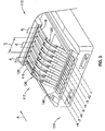
- FIG 1 is a perspective view of an exemplary embodiment of an electrical connector 100.
- the connector 100 is a modular connector, such as, but not limited to, an RJ-45 outlet or communication jack.
- the connector 100 is configured to receive and engage a mating or modular plug 145 (shown in Figure 4 ) (also referred to as a mating connector).
- the modular plug 145 is loaded along a mating direction, shown generally by arrow A.
- the connector 100 includes a connector body 101 having a mating end 104 that is configured to receive and engage the modular plug 145 and a loading end 106 that is configured to electrically and mechanically engage a cable 126.
- the connector body 101 may include a housing 102 extending from the mating end 104 and toward the loading end 106.
- the connector body 101 or housing 102 may at least partially define an interior chamber 108 that extends therethrough and is configured to receive the modular plug 145 proximate the mating end 104.
- the connector 100 includes a contact sub-assembly 110 received within the housing 102 proximate to the loading end 106.
- the contact sub-assembly 110 is secured to the housing 102 via tabs 112 that cooperate with corresponding openings 113 within the housing 102.
- the contact sub-assembly 110 extends from a mating end portion 114 to a terminating end portion 116.
- the contact sub-assembly 110 is held within the housing 102 such that the mating end portion 114 of the contact sub-assembly 110 is positioned proximate the mating end 104 of the housing 102.
- the terminating end portion 116 in the exemplary embodiment is located proximate to the loading end 106.
- the contact sub-assembly 110 includes an array 117 of mating conductors or contacts 118.
- Each mating conductor 118 within the array 117 includes a mating surface 120 arranged within the chamber 108.
- the mating conductors 118 extend between the corresponding mating surfaces 120 and corresponding conductor vias 139 ( Figure 2 ) in a printed circuit 132 ( Figure 2 ).
- Each mating surface 120 engages (i.e., interfaces with) a select mating or plug contact 146 (shown in Figure 4 ) of the modular plug 145 when the modular plug 145 is mated with the connector 100.
- the arrangement of the mating conductors 118 may be at least partially determined by industry standards, such as, but not limited to, International Electrotechnical Commission (IEC) 60603-7 or Electronics Industries Alliance / Telecommunications Industry Association (EIA/TIA)-568.
- IEC International Electrotechnical Commission
- EIA/TIA Electronics Industries Alliance / Telecommunications Industry Association
- the connector 100 includes eight mating conductors 118 comprising four differential pairs.
- the connector 100 may include any number of mating conductors 118, whether or not the mating conductors 118 are arranged in differential pairs.
- a plurality of cable wires 122 are attached to terminating portions 124 of the contact sub-assembly 110.
- the terminating portions 124 are located at the terminating end portion 116 of the contact sub-assembly 110.
- Each terminating portion 124 may be electrically connected to a corresponding one of the mating conductors 118.
- the wires 122 extend from the cable 126 and are terminated at the terminating portions 124.
- the terminating portions 124 include insulation displacement contacts (IDCs) for electrically connecting the wires 122 to the contact sub-assembly 110.
- IDCs insulation displacement contacts
- the wires 122 may be terminated to the contact sub-assembly 110 via a soldered connection, a crimped connection, and/or the like.
- eight wires 122 arranged as differential pairs are terminated to the connector 100.
- any number of wires 122 may be terminated to the connector 100, whether or not the wires 122 are arranged in differential pairs.
- Each wire 122 is electrically connected to a corresponding one of the mating conductors 118.
- the connector 100 may provide electrical signal, electrical ground, and/or electrical power paths between the modular plug 145 and the wires 122 via the mating conductors 118 and the terminating portions 124.
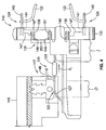
- FIG 2 is a perspective view of an exemplary embodiment of the contact sub-assembly 110.
- the contact sub-assembly 110 includes a base 130 extending from the mating end portion 114 to a printed circuit 132 proximate the terminating end portion 116, which is located proximate to the loading end 106 ( Figure 1 ) when the connector 100 ( Figure 1 ) is fully assembled.
- the term "printed circuit” includes any electric circuit in which conductive pathways have been printed or otherwise deposited in predetermined patterns on a dielectric substrate.
- the printed circuit 132 may be a circuit board or a flex circuit having a substrate 202.
- the contact sub-assembly 110 holds the array 117 of mating conductors 118 such that the mating conductors 118 extend in a direction that is generally parallel to the loading direction (shown in Figure 1 by arrow A) of the modular plug 145 ( Figure 4 ).
- the base 130 includes a supporting block 134 positioned proximate to the printed circuit 132 and a band 133 of dielectric material that is configured to facilitate supporting or holding the mating conductors 118 in a predetermined arrangement.
- the printed circuit 132 may electrically engage the mating conductors 118 through corresponding conductor vias 139 and shielded vias 151 (shown in Figure 5 ).
- the mating conductors 118 may have circuit contact portions 252 proximate to the printed circuit 132 that electrically connect to the corresponding conductor and shielded vias 139 and 151.
- the conductor and shielded vias 139 and 151 may be electrically connected to corresponding terminal vias 141 through corresponding traces (e.g., traces 481-488 shown in Figure 12 ).
- Adjacent mating conductors 118 may have coupling regions 138 that are configured to capacitively couple to one another.
- a "coupling region" of a mating conductor includes dimensions that are configured to substantially affect the electromagnetic coupling of the corresponding mating conductor to other mating conductors and/or the printed circuit.
- the circuit contact portions 252 include the coupling regions 138; however, the coupling regions 138 may be in other portions of the mating conductors 118 in other embodiments.
- the coupling regions 138 may be located proximate to the printed circuit 132.
- the terminal vias 141 may be electrically connected to a plurality of terminal contacts 143 (shown in Figure 4 ). Each terminal contact 143 may mechanically engage and electrically connect to a select wire 122 ( Figure 1 ) proximate the loading end 106 ( Figure 1 ).
- the arrangement or pattern of the conductor and shielded vias 139 and 151 with respect to each other and to the terminal vias 141 within the printed circuit 132 may be configured for a desired electrical performance.
- the traces (described below) that electrically connect the terminal vias 141 to the conductor and shielded vias 139 and 151 may also be configured to tune or obtain a desired electrical performance of the connector 100.
- the contact sub-assembly 110 may also include a compensation component 140 (indicated by dashed-lines) that extends between the mating end portion 114 and the terminating end portion 116.
- the compensation component 140 may be received within a cavity 142 of the base 130.
- the mating conductors 118 may be electrically connected to the compensation component 140 proximate to the mating end portion 114 and/or the terminating end portion 116.
- the mating conductors 118 may be electrically connected to the compensation component 140 through contact pads 144 proximate to the mating end portion 114.
- the mating conductors 118 may also be electrically connected to the compensation component 140 through other contact pads (not shown) located toward the terminating end portion 116 of the compensation component 140.
- Figure 3 is an enlarged perspective view of the mating end portion 114 of the contact sub-assembly 110.
- the array 117 may include eight mating conductors 118 that are arranged as a plurality of differential pairs P1-P4.
- Each differential pair P1-P4 consists of two associated mating conductors 118 in which one mating conductor 118 transmits a signal current and the other mating conductor 118 transmits a signal current that is about 180° out of phase with the associated mating conductor.
- the differential pair P1 includes mating conductors +4 and -5; the differential pair P2 includes mating conductors +6 and -3; the differential pair P3 includes mating conductors +2 and -1; and the differential pair P4 includes mating conductors +8 and -7.
- the (+) and (-) represent positive and negative polarities of the mating conductors.
- a mating conductor labeled (+) is opposite in polarity to a mating conductor labeled (-), and, as such, the mating conductor labeled (-) carries a signal that is about 180° out of phase with the mating conductor labeled (+).
- Mating conductors may also be characterized as having a signal path or a return path where the signal and return paths carry signals that are about 180° out of phase with each other.
- the mating conductors +6 and -3 of the differential pair P2 are separated by the mating conductors +4 and -5 that form the differential pair P1. As such, the mating conductors +6 and -3 of the differential pair P2 are split by the mating conductors +4 and -5 of the differential pair P 1.
- Near-end crosstalk may develop between the differential pairs P1 and P2 when the plug contacts 146 engage the select mating conductors 118 along the corresponding mating surfaces 120.
- FIG 4 is a schematic side view of the contact sub-assembly 110 when the modular plug 145 is engaged with the connector 100 ( Figure 1 ).
- Each mating conductor 118 may extend along the mating direction A between a plug contact engagement portion 127 and the circuit contact portion 252 that electrically connects to the corresponding conductor vias 139.
- the engagement portion 127 includes the mating surface 120.
- the engagement portion 127 and the circuit contact portion 252 are separated by a length of the corresponding mating conductor 118.
- the band 133 and/or a transition region may be located between the engagement portion 127 and the circuit contact portion 252.
- the engagement portion 127 is configured to interface with the corresponding plug contact 146 along the mating surface 120, and the circuit contact portion 252 is configured to be electrically connected to the printed circuit 132. Although not shown, the circuit contact portion 252 may also be electrically connected to the compensation component 140 ( Figure 2 ).
- the plug contacts 146 of the modular plug 145 are configured to selectively engage mating conductors 118 of the array 117. When the plug contacts 146 engage the mating conductors 118 at the corresponding mating surfaces 120, offending signals that cause noise/crosstalk may be generated.
- the offending crosstalk (NEXT loss) is created by adjacent or nearby conductors or contacts through capacitive and inductive coupling which yields the unwanted exchange of electromagnetic energy between a first differential pair and or signal conductor to second differential pair and or signal conductor.
- the circuit contact portions 252 may include end portions 149 that are mechanically engaged and electrically connected to corresponding shielded and conductor vias 151 and 139 of the printed circuit 132.
- the terminating portions 124 may include the terminal vias 141 electrically connected to corresponding terminal contacts 143.
- the shielded and conductor vias 151 and 139 are electrically connected to select terminal vias 141 through traces 147 of the printed circuit 132.
- Each terminal via 141 may be electrically connected to a terminal contact 143, which are illustrated as IDC's in Figure 4 .
- the terminal contacts 143 mechanically engage and electrically connect to corresponding wires 122.
- the printed circuit 132 may interconnect the mating conductors 118 to the terminal contacts 143 and transmit signal current therethrough.
- the coupling regions 138 may be arranged and configured with respect to each other to improve the performance of the connector 100 ( Figure 1 ).
- the conductor vias 139, the shielded vias 151, and the terminal 141 may be arranged with respect to each other to improve the performance of the connector 100.
- the traces 147 of the printed circuit 132, the compensation component 140, and the arrangement of the mating conductors 118 may also be configured to improve the performance of the connector 100.
- the mating conductors 118 form at least one interconnection path, such as the interconnection path X1, that transmits signal current between the mating end 104 ( Figure 1 ) and the loading end 106 ( Figure 1 ).
- the interconnection path X1 may extend between the engagement portions 127 of the mating conductors 118 and the circuit contact portions 252 to the corresponding conductor and shielded vias 139 and 151.
- another interconnection path may extend between the conductor and shielded vias 139 and 151, the PCB traces 147, the terminal vias 141, and to the terminal contacts 143.
- An "interconnection path,” as used herein, is collectively formed by mating conductors and/or traces of a differential pair(s) that are configured to transmit a signal current between corresponding input and output terminals or nodes when the electrical connector is in operation.
- the mating conductors and/or traces experience crosstalk coupling from each other that may be used for compensation to reduce or cancel the offending crosstalk and/or to improve the overall performance of the connector.
- the signal current may be a broadband frequency signal current.
- each differential pair P1-P4 ( Figure 3 ) transmits signal current along the interconnection path X1 between the corresponding engagement portion 127 and the corresponding circuit contact portion 252.
- another interconnection path may extend through the compensation component 140 ( Figure 2 ). Such embodiments are described in greater detail in US Patent No. 7,914,345 .
- the interconnection path X1 may include one or more NEXT stages.
- a “NEXT stage,” as used herein, is a region where signal coupling (i.e., crosstalk coupling) exists between conductors or pairs of conductors of different differential pairs or signal paths and where the magnitude and phase of the crosstalk are substantially similar, without abrupt change.
- the NEXT stage could be a NEXT loss stage, where offending signals are generated, or a NEXT compensation stage, where NEXT compensation is provided.
- the interconnection path X1 may include a NEXT loss Stage 0 and a NEXT compensation Stage I. The Stages 0 and I are separated by the transition region 135.
- FIG 5 is an elevation view of the printed circuit 132 as viewed from the loading end 106 ( Figure 1 ) and illustrating the terminal vias 141, the conductor vias 139, and the shielded vias 151 arranged with respect to each other in the exemplary embodiment.
- the printed circuit 132 includes the substrate 202 having a length L 1 that extends along a vertical or first orientation axis 190 and a width W 1 that extends along a horizontal or second orientation axis 192.
- the terms “horizontal” and “vertical” are used only for describing orientation and not intended to limit the embodiments described herein.
- the substrate 202 has a substantially rectangular and planar body and a surface S 1 extending therealong.
- the substrate 202 includes side edges 210-213.
- the side edges 211 and 213 extend substantially parallel to each other and extend widthwise along the second orientation axis 192.
- the side edges 210 and 212 extend substantially parallel to each other and extend lengthwise along the first orientation axis 190.
- the length L 1 is illustrated as being greater than the width W 1 , in alternative embodiments, the width W 1 may be greater than the length L 1 or the length L 1 and width W 1 may be substantially equal.
- the substrate 202 is shown as being substantially rectangular, the substrate may have other geometric shapes that include curved or planar side edges.
- the substrate 202 may be formed from a dielectric material(s) having multiple layers and include opposite end portions 204 and 206 and a center portion 208 extending therebetween.
- the substrate 202 is configured to interconnect the wires 122 ( Figure 1 ) and the mating conductors 118 ( Figure 1 ) so that current may flow therethrough.
- the conductor and shielded vias 139 and 151 are configured to electrically connect with corresponding mating conductors 118, and the terminal vias 141 are configured to electrically connect with the terminal contacts 143 ( Figure 4 ).
- the conductor vias 139, the shielded vias 151, and the terminal vias 141 may form the differential pairs P1-P4 and may be referred to as conductor vias 1-8, shielded vias 1-8, or terminal vias 1-8.
- the shielded vias 151 are electrically connected to the mating conductors 118 of the differential pair P2.
- the conductor vias 139, the shielded vias 151, and the terminal vias 141 are configured to transmit signal current of the differential pairs P1-P4 ( Figure 3 ).
- the substrate 202 may include a circuit array 224 that includes the plurality of conductor vias 139, the pair of shielded vias 151, and the plurality of terminal vias 141 arranged with respect to each other to for mitigating offending crosstalk and/or improving return loss.
- the plurality of conductor vias 139 and the pair of shielded vias 151 may form an interior array 220 and the plurality of terminal vias 141 may form an outer ring 221 (shown in Figure 6 ) having outer ring portions 222A and 222B.
- the shielded vias 151 are the vias -3 and +6 associated with the differential pair P2 (i.e., the pair of shielded vias 151 are electrically connected to the mating conductors 118 of differential pair P2).
- the interior array 220 may also include first and second shielding rows 230 and 232 of conductor vias 139 that are located to isolate and shield the shielded vias 151 from the terminal vias 141.
- the first and second shielding rows 230 and 232 of conductor vias 139 are located between the end portions 204 and 206.
- the shielded vias -3 and +6 of the differential pair P2 may be centrally located in the circuit array 224.
- the term "centrally located” includes the shielded vias -3 and +6 being located generally near a center 226 of the circuit array 224 (or the outer ring 221 shown in Figure 6 ) and surrounded by the conductor vias 139 and terminal vias 141.
- the shielded vias 151 may be adjacent to one another.
- two vias are "adjacent" to one another when the two vias are relatively close to each other and no other via is located therebetween.
- the shielded vias -3 and +6 of the differential pair P2 are adjacent; the terminal vias -3 and +6 of the differential pair P2 are adjacent; the terminal vias -5 and +4 of the differential pair P1 are adjacent; the terminal vias -7 and +8 of the differential pair P4 are adjacent; the terminal vias -1 and +2 of the differential pair P3 are adjacent.
- vias that are not of a differential pair may be adjacent.
- the conductor via -5 is adjacent to the conductor via +2 and the conductor via +8.
- the conductor via +2 is adjacent to the terminal via +6, and the conductor via -7 is adjacent to the terminal via -1.
- the first and second shielding rows 230 and 232 are configured to electrically isolate the shielded vias 151 from the outer ring 221 (shown in Figure 6 ) of surrounding terminal vias 141. As such, the pair of shielded vias 151 is located between the first and second shielding rows 230 and 232. As shown, the conductor vias 139 of the first shielding row 230 are distributed widthwise (i.e., spaced apart from each other) along a first row axis 240. The first row axis 240 may extend substantially parallel to the second orientation axis 192.
- the conductor vias 139 of the first shielding row 230 are substantially aligned with respect to each other along the first row axis 240 such that the first row axis 240 intersects the corresponding conductor vias 139.
- the first row axis 240 intersects centers of the conductor vias 139; however, the conductor vias 139 may be substantially aligned with respect to each other provided that the first row axis 240 intersects at least a portion of the each conductor via 139 of the first shielding row 230.
- the conductor vias 139 of the second shielding row 232 are distributed widthwise along a second row axis 242.
- the first and second row axes 240 and 242 may extend substantially parallel to each other and the second orientation axis 192.
- the conductor vias 139 of the second shielding row 232 are substantially aligned with respect to each other along the second row axis 242.
- each of the centrally located shielded vias 151 may be substantially equidistant from the first and second shielding rows 230 and 232. More specifically, the shielded vias -3 and +6 may be spaced apart from each other and located along a central-pair axis 244 that extends substantially parallel to the first and second row axes 240 and 242. A shortest distance Z 1 measured from the shielded via -3 to the first row axis 240 may be substantially equidistant to a shortest distance Z 2 measured from the shielded via -3 to the second row axis 242. In the illustrated embodiment, the distance Z 1 is slightly greater than the distance Z 2 . Likewise, the shielded via +6 may be substantially equidistant from the first and second row axes 240 and 242.
- Each end portion 204 and 206 may include one of the outer ring portions 222A and 222B, respectively, which each include corresponding terminal vias 141 of the outer ring 221 (shown in Figure 6 ).
- each differential pair P1-P4 of terminal vias 141 i.e., terminal vias -5 and +4; -3 and +6; -1 and +2; -7 and +8; respectively
- the interior array 220 is located between the terminal vias 141 of the outer ring portions 222A and 222B.
- the terminal vias 141 within each end portion 204 and 206 are distributed in a direction along the second orientation axis 192 (or in a direction along the first and second row axes 240 and 242).
- the terminal vias 141 may be spaced apart from each other in a direction along the second orientation axis 192 such that the terminal vias 141 may have more than two axial locations with respect to the second orientation axis 192 (i.e., the terminal vias 141 may be located on more than two axes that extend substantially parallel to the first orientation axis 190).
- Figure 5 illustrates a particular embodiment where there are four axial locations 171-174.
- each terminal via 141 within the end portion 204 has its own axial location with respect to the second orientation axis 192
- each terminal via 141 within the end portion 206 has its own axial location with respect to the second orientation axis 192.
- no two terminal vias 141 may be substantially aligned along an axis that extends substantially parallel to the first orientation axis 190.
- the terminal vias 141 may have only two or three axial locations. Furthermore, two terminal vias may be substantially aligned with respect to an axis that extends parallel to the first orientation axis 190 in other embodiments.
- Figure 6 is the elevation view of the printed circuit 132 from Figure 5 and also illustrates the arrangement of the terminal vias 141, the shielded vias 151, and the conductor vias 139 in the circuit array 224.
- the substrate 202 may extend along center axes 290 and 292 that intersect the center 226 of the circuit array 224. (The center 226 of the circuit array 224 may or may not overlap a geometric center of the substrate 202.)
- the center axis 290 extends parallel to the first orientation axis 190, and the center axis 292 extends parallel to the second orientation axis 192.
- the terminal vias 141 may be arranged such that differential pairs P1-P4 of terminal vias 141 are symmetrical with respect to each other about the center axes 290 and 292.
- terminal vias 141 of the differential pairs P1-P4 are arranged such that the terminal vias 141 of the differential pairs P1-P4 form the substantially circular-shaped outer ring 221 (indicated by a dashed outline).
- the outer ring 221 surrounds the interior array 220 of the conductor and shielded vias 139 and 151.
- each differential pair P1-P4 of terminal vias 141 may be located on a corresponding plane M 1 -M 4 , respectively.
- the planes M 1 -M 4 may substantially face the interior array 220 (i.e., lines drawn perpendicular to the planes M 1 -M 4 extend toward the interior array 220).
- Each plane M 1 -M 4 may face a different direction with respect to the other planes M 1 -M 4 .
- Each plane M 1 -M 4 may also face the center 226 or the centrally located shielded vias -3 and +6. More specifically, a line drawn from any point between associated terminal vias 141 along the respective plane M 1 -M 4 to the center 226 may be substantially perpendicular to the respective plane M 1 -M 4 (e.g., about 90° +/- 10°). In alternative embodiments, only one, two, or three planes M face the center 226.
- At least two planes M may oppose each other (i.e., face each other) with the center 226 between the terminal vias 141. Also shown in Figure 6 , the planes M 1 -M 4 may be equidistant from the center 226. However, in alternative embodiments, one or more planes M are not equidistant with respect to the other.
- each differential pair P1-P4 may be adjacent to each other and separated from each other by a separation distance S D .
- the separation distances S D1 -S D4 of the differential pairs P1-P4, respectively, are substantially equal.
- the separation distances S D1 -S D4 are not substantially equal.
- each separation distance S D1 -S D4 may have a midpoint 261-264 between the associated terminal vias 141 and located on the respective plane M 1 -M 4 .
- Each plane M 1 -M 4 may be tangent to the outer ring 221 at the corresponding midpoint 261-264, respectively. As shown in Figure 6 , lines drawn from the midpoints 261-264 may be substantially perpendicular to the center 226.
- the terminal vias 141 of one differential pair may be substantially equidistant from one of the conductor vias 139 of the first or second shielding row 230 and 232.
- the conductor via -1 of the shielding row 232 may be substantially equidistant from the terminal vias +8 and - 7 of the differential pair P4.
- Figure 5 shows that each conductor via 139 of the first and second shielding rows 230 and 232 may be separated from the shielded vias -3 and +6 by predetermined distances D via-to-via .
- the distances D via-to-via are measured from a center of one via to a center of the other via.
- Figure 6 shows that the associated conductor vias 139 of each differential pair P1-P4 may be separated from each other by predetermined distances D via-to-via .
- Table 1 lists the respective distances D via-to-via for the particular embodiment shown in Figures 5 and 6 .
- the conductor vias +2, -5, and +8 of the first shielding row 230 may be evenly spaced apart from each other along the first row axis 240.
- the conductor vias -1, +4, and -7 of the second shielding row 232 may be evenly spaced apart from each other along the second row axis 242.
- the distances D via-to-via extending from the conductor vias 139 of the first shielding row 230 to the centrally located shielded vias -3 and +6 may be substantially equal (i.e., within approximately 30% of each other or, in a more specific embodiment, 20%).
- the distances D via-to-via extending from the conductor vias 139 of the second shielding row 232 to the centrally located shielded vias -3 and +6 may be substantially equal (i.e., within approximately 30% of each other or, in a more specific embodiment, 20%).
- the distance D 36 ( Figure 6 ) separating the shielded vias -3 and +6 may be approximately equal to the distances separating the conductor vias 139 along each shielding row.
- the distance D 36 also extends along the central-pair axis 244. Accordingly, the distance or length of the first shielding row 230 (i.e., D 25 + D 58 ) is greater than the distance D 36 ( Figure 6 ) separating the shielded vias -3 and +6.
- the distance or length of the second shielding row 232 i.e., D 14 + D 47 ) is greater than the distance D 36 .
- the distance D 36 may be less than the shortest distances Z 1 and Z 2 .
- the distance D via-to-via that separates the associated conductor vias 139 of one differential pair P1, P3, and P4 (i.e., D 45 , D 12 , D 78 ) in the interior array 220 may be substantially equal (e.g., the distance D via-to-via separating the conductor vias 139 of the differential pairs P1, P3, and P4 is equal to 6.876 mm in Table 1).
- the distance D via-to-via that separates the associated conductor vias 139 of a differential pair may also be used to determine the differential characteristic impedance between the associated conductor vias 139.
- the differential characteristic impedance of the conductor vias 139 may be determined by the radius of the conductor vias 139 and the D via-to-via between the associated mating conductors 118.
- At least one of the shielded vias 151 may form a "dual-polarity" coupling with two conductor vias 139.
- the respective shielded via 151 electromagnetically couples with two conductor vias 139.
- the respective shielded via 151 may electromagnetically couple with two conductor vias 139 in which the two conductor vias 139 have opposite signs with respect to each other. Dual-polarity coupling may facilitate in the reduction of offending crosstalk coupling that may occur between the conductor vias 139, shielded vias 151, and the terminal vias 141 in the printed circuit 132.
- the shielded via 151 may electromagnetically couple with two conductor vias 139 of the same differential pair.
- the shielded via -3 is electromagnetically coupled with the conductor via +2, which has an opposite sign polarity, and is also electromagnetically coupled with the conductor -1, which has the same sign polarity.
- the shielded via +6 is electromagnetically coupled with the conductor via +8, which has the same sign polarity, and is also electromagnetically coupled with the conductor -7, which has the opposite sign polarity.
- the conductor vias 139 that form a dual-polarity coupling are equivalent in size (i.e., they have a common diameter).
- the shielded via 151 may form a dual-polarity coupling with conductor vias 139 of a differential pair in which each shielding row 230 and 232 has one of the conductor vias 139 of the corresponding differential pair.
- the distance separating the electrically isolated shielded via 151 from the corresponding two dual-polarity conductor vias 139 may be substantially equidistant.
- first and second conductor vias +2 and -1 of the differential pair P3 may be located first and second distances away (i.e., distances D 13 and D 23 ), respectively, from the shielded via -3.
- a difference between the first and second distances may be at most 30% of one of the first and second distances.
- the difference between the first and second distances may be at most 20% of one of the first and second distances.
- distance D 68 may be substantially equal to distance D 67 . Accordingly, the electromagnetic coupling between the shielded via -3 and the conductor vias +2 and -1 may be substantially balanced, and the electromagnetic coupling between the shielded via +6 and the conductor vias +8 and -7 may be substantially balanced.
- each shielded via -3 and +6 may be electromagnetically coupled to another differential pair.
- both of the shielded vias -3 and +6 may be electromagnetically coupled to the conductor vias -5 and +4 of the differential pair P1.
- the shielded vias -3 and +6 may each form a dual-polarity coupling with the conductor vias -5 and +4.
- the first and second rows 230 and 232 may not only electrically isolate the shielded vias -3 and +6 from the terminal vias 141, but may also electromagnetically couple in a balanced manner to the shielded vias -3 and +6.
- FIG 7 is an elevation view of a printed circuit 632 formed in accordance with an alternative embodiment that may be used with the connector 100 of Figure 1 .
- the printed circuit 632 may have similar features as the printed circuit 132 shown in Figures 5 and 6 .
- the printed circuit 632 may have a substrate 602 that is similar to the substrate 202 ( Figure 5 ).
- the substrate 602 may have terminal vias 641 that are similarly arranged as the terminal vias 141 ( Figure 5 ).
- the printed circuit 632 may include an interior array 620 of conductor vias 639 and shielded vias 651 that is different than the interior array 220 ( Figure 5 ) of the printed circuit 132.
- the conductor vias 639 and the shielded vias 651 may be electrically connected to the mating conductors 118 ( Figure 1 ), which form the differential pairs P1-P4 ( Figure 3 ).
- the conductor vias 639 may form first and second shielding rows 650 and 652.
- the conductor vias 639 of each shielding row 650 and 652 may be substantially aligned with respect to each other.
- the conductor vias 639 of the differential pair P3 may be switched with respect to the conductor vias 139 ( Figure 5 ) of the differential pair P3.
- the conductor via -1 is substantially aligned with the conductor vias -5 and +8 in the first shielding row 650
- the conductor via +2 is substantially aligned with the conductor vias +4 and -7 in the second shielding row 652.
- the conductor vias 639 of each shielding row 650 and 652 are not evenly spaced apart from each other as the conductor vias 139 are in first and second shielding rows 230 and 232 ( Figure 5 ).
- the interior array 620 of conductor vias 639 and shielded vias 651 may be separated by distances D via-to-via as listed in Table 2.
- the first and second shielding rows 650 and 652 of conductor vias 639 may be configured to electrically isolate the centrally located shielded vias 651 from the terminal vias 641. Furthermore, each shielded via -3 and +6 may form a dual-polarity coupling with the conductor vias 639 of the first and second shielding rows 650 and 652. As shown, each shielded vias 651 may be electromagnetically coupled to the conductor vias 639 of one differential pair.
- the shielded via -3 is electromagnetically coupled with the conductor vias +2 and -1 (i.e., the conductor vias 139 of the differential pair P3)
- the shielded via +6 is electromagnetically coupled with the conductor vias +8 and -7 (i.e., the conductor vias 139 of the differential pair P4).
- the distance D via-to-via separating the shielded via -3 from conductor vias -1 and +2 may be substantially equal
- the distance D via-to-via separating the shielded via +6 from conductor vias +8 and -7 may be substantially equal.
- the electromagnetic coupling among the conductor vias 639 may be configured as desired.
- Figures 5-7 illustrate particular embodiments for electrically isolating the shielded vias of the differential pair P2 and/or for forming a dual-polarity coupling with the conductor vias of the shielding rows, other embodiments having different configurations, dimensions, and distances D via-to-via may be made.
- FIG 8A is an exposed perspective view of the printed circuit 132 and the array 117 of mating conductors 118 of the contact sub-assembly 110 ( Figure 1 ).
- the mating conductors 118 may extend from distal tips 250 that are configured to engage the contact pads 144 ( Figure 2 ) and extend toward the printed circuit 132. As shown, each mating conductor 118 may extend from a corresponding distal tip 250 through the plug contact engagement portion 127. The mating conductor 118 may then extend through the transition region 135 where the mating conductor 118, optionally, may be switched or cross-over another mating conductor.
- the mating conductor 118 may extend to a bridge portion 256 and then to the circuit contact portion 252 that mechanically and electrically engages the printed circuit 132. As will be described in greater detail, when the mating conductor 118 extends from the engagement portion 127 toward the printed circuit 132, the mating conductor 118 may form or shape into the coupling region 138. More specifically, the bridge portions 256 and/or the circuit contact portions 252 may include the coupling regions 138.
- Figures 8B and 8C show cross-sections CA 1 and CB 1 of two adjacent mating conductors 118A and 118B.
- Figure 8B illustrates cross-sections CA 1 taken with the corresponding bridge portions 256 ( Figure 8A ) of the adjacent mating conductors 118A and 118B.
- Figure 8C illustrates cross-sections CB 1 taken with coupling regions 138 ( Figure 8A ) of the adjacent mating conductors 118A and 118B.
- the coupling regions 138 are shown as being within the circuit contact portions 252. However, in alternative embodiments, the coupling regions 138 may be in other portions of the mating conductors 118, such as the bridge portion.
- the coupling region 138 of a mating conductor 118 may have an increased surface area SA 1 along a side 254A with respect to other portions of the mating conductor 118 (e.g., with respect to the engagement portion 127, distal tip 250).
- the coupling region 138 may have an increased surface area SA 1 with respect to a surface area SA 2 of the bridge portion 256.
- the surface area SA of the coupling regions appears to be indicated as one dimension in the cross-sections.
- a surface area SA of a planar surface is the product of two dimensions and that the other dimension of the coupling regions that is not shown in the cross-sections of Figures 8-10 is a length in which the adjacent mating conductors extend alongside each other in the coupling regions.
- the coupling regions 138 of adjacent mating conductors 118A and 118B may increase the capacitive coupling between the adjacent mating conductors 118A and 118B thereby affecting the crosstalk coupling of the connector 100.
- the surface area SA of each coupling region 138 may be configured to create desired compensatory crosstalk that may reduce or cancel the offending crosstalk coupling that occurs at the plug contacts 146 and/or mating surfaces 120 of the engagement portions 127.
- the surface area SA of each coupling region 138 may be approximately equal to surface areas of the plug contacts 146 ( Figure 4 ) that face each other when the modular plug 145 ( Figure 4 ) engages the connector 100.
- the mating conductors 118A and 118B are adjacent to one another and extend alongside each other. As shown, the mating conductors 118A and 118B have a spacing S 5 therebetween. In alternative embodiments, the spacing S 5 may vary as desired as varying the spacing S 5 may affect the electromagnetic coupling of the adjacent mating conductors 118A and 118B. However, in the illustrated embodiment, the spacing S 5 is uniform from the transition region 135 to the printed circuit 132. Furthermore, each mating conductor 118 has opposite sides 254A and 254B and opposite edges 258A and 258B. The side 254A of one mating conductor 118 may face the side 254B of another mating conductor 118.
- the mating conductors 118A and 118B may have a uniform width W 2 at the cross-sections CA 1 and CB 1 .
- the mating conductors 118A and 118B may have a thickness T 1 ( Figure 8B ) at the cross-section CA 1 and a thickness T 2 ( Figure 8C ) at the cross-section CB 1 .
- the thickness T 2 is greater along the coupling region 138 than the thickness T 1 at the bridge portion 256.
- the thickness T 1 may be less than the width W 2 at the bridge portion 256, but the thickness T 2 may be greater than the width W 2 at the coupling region 138 (and also greater than the thickness T 1 in the bridge portion 256).
- a surface area SA 1 along the sides 254 of the cross-section CB 1 is greater than a surface area SA 2 along the sides 254 of the cross-section CA 1 .
- the surface areas SA 1 may be sized and shaped for a desired amount of crosstalk coupling. For example, the greater the surface area SA 1 , the greater an amount of crosstalk coupling may be generated.
- FIG 9A is an exposed perspective view of a printed circuit 332 and an array 317 of mating conductors 318 of a contact sub-assembly (not shown) formed in accordance with another embodiment.
- the contact sub-assembly may be incorporated into an electrical connector, such as the connector 100 ( Figure 1 ).
- Each mating conductor 318 may extend from a corresponding distal tip 350 through a plug contact engagement portion 327 to a transition region 335 of the array 317.
- Each mating conductor 318 may then extend to a bridge portion 356 and then to a circuit contact portion 352 that mechanically and electrically engages the printed circuit 332.
- the bridge portions 356 may include the coupling regions 338.
- Figures 9B, 9C, and 9D show cross-sections CA 2 , CB 2 , and CC, respectively, of two adjacent mating conductors 318A and 318B.
- Figure 9B illustrates cross-sections CA 2 taken within the corresponding engagement portions 327 ( Figure 9A );
- Figure 9C illustrates cross-sections CB 2 taken within coupling regions 338 in the bridge portions 356 ( Figure 9A );
- Figure 9D illustrates cross-sections CC taken with the circuit contact portions 352 ( Figure 9A ) that engage the printed circuit 332 ( Figure 9A ).
- the mating conductors 318A and 318B are adjacent to one another and extend alongside each other.
- the mating conductors 318A and 318B have a uniform spacing S 2 therebetween ( Figures 9B-9D ).
- each mating conductor 318 has opposite sides 354A and 354B and opposite edges 358A and 358B.
- the side 354A of one mating conductor 318 may face the side 354B of another mating conductor 318.
- the mating conductors 318 may have a uniform width W 3 at the engagement portion 327 ( Figure 9B ), the coupling region 338 ( Figure 9C ), and the circuit contact portion 352 ( Figure 9D ).
- the mating conductors 318 may have a thickness T 3 ( Figure 9B ) at the engagement portion 327, a thickness T 4 ( Figure 9C ) at the coupling region 338 (or bridge portion 356), and a thickness T 5 ( Figure 9D ) at the circuit contact portion 352.
- the thickness T 4 is greater along the coupling region 338 than the thicknesses T 3 and T 5 .
- the thickness T 3 is less than the width W 3 at the engagement portion 327
- the thickness T 5 is less than the width W 3 at the circuit contact portion 352.
- the thickness T 4 is greater than the width W 3 at the bridge portion 356.
- the coupling regions 338 of the mating conductors 318 may have an increased surface area SA along the sides 354 with respect to other portions of the mating conductor 318.
- a surface area SA 4 along the sides 354 of the bridge portions 356 is greater than a surface area SA 3 along the sides 354 of the bridge portions 356 and greater than a surface area SA 5 along the sides 354 of the circuit contact portions 352.
- the surface area SA 4 may be sized and shaped for a desired amount of crosstalk coupling.
- the coupling regions 338 may be positioned a distance away or spaced apart from the printed circuit 332.
- Figure 10 is a perspective view of a printed circuit 438 and an array 417 of circuit contacts 419 that are mechanically and electrically engaged to the printed circuit 438.
- the printed circuit 438 and the array 417 may be components of a contact sub-assembly (not shown) that may be incorporated into an electrical connector, such as the connector 100 ( Figure 1 ).
- the circuit contacts 419 may be separate or discrete with respect to mating contacts (not shown) that electrically and mechanically engage the circuit contacts 419.
- the term "mating conductor” includes unitary mating conductors, such as the mating conductors 118 ( Figures 8A-8C ) and 318 ( Figures 9A-9D ), as well as mating conductors that are formed by separate circuit contacts 419 and mating contacts that are mechanically and electrically engaged to each other.
- Such embodiments that include circuit contacts 419 are described in greater detail in U.S. Patent Application No. 12/547,321 having Attorney Docket No. TO-00272 (958-184), filed contemporaneously herewith.
- each circuit contact 419 may have a beam 440 or 441 that extends along a surface S 3 of a substrate 442 of the printed circuit 438.
- the beams 440 and 441 extend directly alongside the surface S 3 .
- Each circuit contact 419 may include a mating contact engagement portion 444 having a slot 446 defined by opposing arms 448 and 450.
- the engagement portion 444 extends away from the surface S 3 toward a mating end (not shown) of the connector.
- the engagement portion 444 is configured to receive and hold an end of a corresponding mating contact (not shown) within the slot 446 to electrically and mechanically engage the circuit contact 419 to the mating contact.
- each circuit contact 419 includes an end portion 452 that is inserted into a conductor via 454 of the substrate 442.
- the end portion 452 may be, for example, an eye-of-needle type pin that mechanically and electrically engages the corresponding circuit contact 419 to the printed circuit 438.
- each circuit contact 419 may include an extension 460 and a gripping element 462 that extend away from the surface S 3 toward the mating end.
- the extension 460 and the gripping element 462 may be spaced apart from each other so that a thickness of a circuit board (not shown) may be held therebetween.
- the gripping element 462 may be configured to engage contact pads on an underside of the circuit board.
- the extension 460 may be configured to engage other components of the connector.
- the circuit contacts 419 of the array 417 may extend parallel to and be spaced apart from each other. More specifically, two adjacent circuit contacts 419 may be separated from each other by a uniform spacing S 4 . In Figure 10 , the circuit contacts 419 are evenly distributed or spaced apart from each other along the surface S 3 of the substrate 442. However, in alternative embodiments, the circuit contacts 419 may not be evenly distributed. The circuit contacts 419 may also extend parallel to the surface S 3 .
- the circuit contacts 419 may include coupling regions that are configured to electromagnetically couple to coupling regions on other circuit contacts 419.
- an entirety of the circuit contact 419 may be considered a coupling region since the circuit contacts 419 may have greater dimensions than the mating contacts. More specifically, sides of the circuit contacts 419 that face each other may have a greater surface area than sides of the mating contacts that face each other in the interior chamber (not shown).
- the circuit contacts 419 may have varying cross-sections therealong to generate a desired crosstalk coupling similar to the embodiments described above.
- the circuit contacts 419 may have cross-sections CB 3 and CA 3 as shown in Figure 10 in which the circuit contacts 419 at the cross-sections CA 3 have a greater surface area than a surface area of the circuit contacts 419 at the cross-sections CB 3 .
- Figure 11 is a front elevation view of the circuit contacts 419 extending alongside the surface S 3 of the printed circuit 438.
- the printed circuit 438 may have the same configuration of vias as the printed circuit 132 shown in Figures 5 and 6 .
- the circuit contact portions 252 and 352 may have similar features.
- a time delay between adjacent circuit contacts 419 may be formed to create a phase imbalance and to improve the electrical performance of the connector 100 ( Figure 1 ).
- the imbalance may be used to improve return loss and/or generate a desired amount of crosstalk coupling.
- the differential signals of the differential pairs P1-P4 ( Figure 3 ) may be phase matched ⁇ 0 at a location where a reference plane P REF intersects each circuit contact 419.
- Each circuit contact 419 forms an interconnection path or conductive pathway that extends a predetermined length LC from the reference plane P REF .
- the conductive pathways may extend parallel to the surface S 3 and with respect to each other.
- the predetermined length LC may be different for each circuit contact 419 and represents a length that current must flow along the corresponding conductive pathway between the reference plane P REF and a corresponding conductor via 454.
- the arrows extending from the reference plane P REF indicate the conductive pathways through each circuit contact 419. In the illustrated embodiment, the conductive pathways extend parallel to each other and the surface S 3 .
- the conductive pathways associated with the circuit contacts -3 and +6 may extend a length LC 1 and have a phase measurement ⁇ 1 ; the conductive pathways associated with the circuit contacts +2, -5, and +8 may extend a length LC 3 and have a phase measurement ⁇ 3 ; and the conductive pathways associated with the circuit contacts -1, +4, and -7 may extend a length LC 2 and have a phase measurement ⁇ 2 .
- the circuit contacts -3 and +6 associated with the differential pair P2 extend a common length, the length LC 1 , and in a common direction away from the reference plane P REF .
- the associated circuit contacts 419 of the differential pairs P1, P3, and P4 may extend in different (e.g., opposite) directions away from the reference plane P REF and along different lengths.
- the conductive pathways associated with the circuit contacts +2, -5, and +8 extend a greater length LC 3 than the length LC 2 of the conductive pathways of the associated circuit contacts -1, +4, and -7 respectively.
- a phase imbalance may be created between the associated circuit contacts 419 of certain differential pairs.
- the phase imbalance may be configured to improve return loss of the connector.
- the phase imbalance may be configured to generate a desired amount of crosstalk coupling.
- circuit contacts 419 do not extend directly alongside the surface S 3 of the substrate 442, but may still create the phase imbalance between the conductive pathways. Furthermore, in other embodiments, the circuit contact portions 252 and 352 may form similar conductive pathways and create similar phase imbalances as described with respect to the circuit contacts 419.
- Figure 12 is a back elevation view of the substrate 442 of the printed circuit 438.
- the substrate 442 may include a plurality of traces 481-488 that interconnect the conductor vias 454 and shielded vias 451 to corresponding terminal contacts 456.
- the traces 481-488 may be configured to offset phase imbalances due to the arrangement and configuration of the circuit contacts 439 as shown in Figure 11 . More specifically, a length of the conductive pathways along the traces 481-488 may be configured to offset the phase imbalances.
- the trace 481 may have a shorter conductive pathway than the trace 482; the trace 485 may have a shorter conductive pathway than the trace 484; and the trace 487 may have a shorter conductive pathway than the trace 488.
- the traces 481-488 may have other configurations.
- the printed circuit 438 may include other components, such as non-ohmic plates or inter-digital fingers, that are configured to facilitate obtaining a desired electrical performance.
Description
- The subject matter herein relates generally to electrical connectors, and more particularly, to electrical connectors that utilize differential pairs and experience offending crosstalk and/or return loss.
- The electrical connectors that are commonly used in telecommunication systems, such as modular jacks and modular plugs, may provide interfaces between successive runs of cable in such systems and between cables and electronic devices. The electrical connectors may include mating conductors that are arranged according to known industry standards, such as Electronics Industries Alliance / Telecommunications Industry Association ("EIA/TIA")-568. However, the performance of the electrical connectors may be negatively affected by, for example, near-end crosstalk (NEXT) loss and/or return loss. In order to improve the performance of the connectors, techniques are used to provide compensation for the NEXT loss and/or to improve the return loss.
- Such techniques have focused on arranging the mating conductors with respect to each other within the electrical connector and/or introducing components to provide the compensation, e.g., compensating NEXT. For example, compensating signals may be created by crossing the conductors such that a coupling polarity between the two conductors is reversed. Compensating signals may also be created in a circuit board of the electrical connector by capacitively coupling digital fingers to one another. However, the above techniques may have limited capabilities for providing crosstalk compensation and/or improving return loss.
- Thus, there is a need for additional techniques to improve the electrical performance of the electrical connector by reducing crosstalk and/or by improving return loss.
-
US 2007/0212946 discloses a receptacle assembly with a housing having front end for receiving a plug, and a rear end for accepting wire termination contacts. A circuit board is held within the housing and has contact holes arranged in a contact array pattern, and wire termination holes arranged in a wire termination pattern. - According to the invention, there is provided an electrical connector as defined in any one of the appended claims. The electrical connector includes an array of mating conductors configured to engage select plug contacts of a modular plug. The mating conductors include differential pairs. The connector also includes a plurality of terminal contacts that are configured to electrically connect to select cable wires and a printed circuit that interconnects the mating conductors to the terminal contacts. The printed circuit has opposite end portions and also includes first and second shielding rows of conductor vias that are located between the end portions and are electrically connected to the mating conductors. The conductor vias of each of the first and second shielding rows is substantially aligned along first and second row axes, respectively. The first and second row axes are substantially parallel to each other. The printed circuit also includes outer terminal vias that are electrically connected to the terminal contacts. Each end portion has terminal vias therein that are distributed in a direction along the first and second row axes. The printed circuit also includes a pair of shielded vias that are electrically connected to corresponding mating conductors. The pair of shielded vias are located between the first and second shielding rows. The electrical connector is characterised in that the pair of shielded vias are located along a central-pair axis extending between the first and second shielding rows, and substantially parallel to the first and second row axes. The conductor vias of the first and second shielding rows are located to electrically isolate the shielded vias from the terminal vias.
- The invention will now be described by way of example with reference to the accompanying drawings in which:
-
Figure 1 is perspective view of an electrical connector formed in accordance with one embodiment. -
Figure 2 is a perspective view of an exemplary embodiment of a contact sub-assembly of the connector shown inFigure 1 . -
Figure 3 is an enlarged perspective view of a mating end of the contact sub-assembly shown inFigure 2 . -
Figure 4 is a schematic side view of a contact sub-assembly when a modular plug is engaged with the connector ofFigure 1 . -
Figure 5 is an elevation view of a printed circuit that may be used with the connector ofFigure 1 . -
Figure 6 is the elevation view of the printed circuit shown inFigure 5 illustrating an arrangement of vias with respect to each other. -
Figure 7 is an elevation view of a printed circuit formed in accordance with another embodiment that may be used with the connector ofFigure 1 . -
Figure 8A is a perspective view of the printed circuit and an array of mating conductors that may be used with the connector ofFigure 1 . -
Figure 8B is a cross-sectional view of bridge portions of adjacent mating conductors ofFigure 8A . -
Figure 8C is a cross-sectional view of coupling regions of adjacent mating conductors ofFigure 8A . -
Figure 9A is a perspective view of a printed circuit and an array of mating conductors in accordance with another embodiment. -
Figure 9B is a cross-sectional view of engagement portions of the adjacent mating conductors ofFigure 9A . -
Figure 9C is a cross-sectional view of coupling regions of the adjacent mating conductors ofFigure 9A . -
Figure 9D is a cross-sectional view of circuit contact portions of the adjacent mating conductors ofFigure 9A . -
Figure 10 is a perspective view of a printed circuit and an array of circuit contacts in accordance with another embodiment. -
Figure 11 is an elevation view of the printed circuit and the array of circuit contacts shown inFigure 10 . -
Figure 12 is an elevation view of the printed circuit shown inFigure 10 showing a plurality of traces extending therethrough. -
Figure 1 is a perspective view of an exemplary embodiment of anelectrical connector 100. In the exemplary embodiment, theconnector 100 is a modular connector, such as, but not limited to, an RJ-45 outlet or communication jack. However, the subject matter described and/or illustrated herein is applicable to other types of electrical connectors. Theconnector 100 is configured to receive and engage a mating or modular plug 145 (shown inFigure 4 ) (also referred to as a mating connector). Themodular plug 145 is loaded along a mating direction, shown generally by arrow A. Theconnector 100 includes aconnector body 101 having amating end 104 that is configured to receive and engage themodular plug 145 and aloading end 106 that is configured to electrically and mechanically engage acable 126. Theconnector body 101 may include ahousing 102 extending from themating end 104 and toward theloading end 106. Theconnector body 101 orhousing 102 may at least partially define aninterior chamber 108 that extends therethrough and is configured to receive themodular plug 145 proximate themating end 104. - The
connector 100 includes acontact sub-assembly 110 received within thehousing 102 proximate to theloading end 106. In the exemplary embodiment, thecontact sub-assembly 110 is secured to thehousing 102 viatabs 112 that cooperate withcorresponding openings 113 within thehousing 102. Thecontact sub-assembly 110 extends from amating end portion 114 to a terminatingend portion 116. Thecontact sub-assembly 110 is held within thehousing 102 such that themating end portion 114 of thecontact sub-assembly 110 is positioned proximate themating end 104 of thehousing 102. The terminatingend portion 116 in the exemplary embodiment is located proximate to theloading end 106. As shown, thecontact sub-assembly 110 includes anarray 117 of mating conductors orcontacts 118. Eachmating conductor 118 within thearray 117 includes amating surface 120 arranged within thechamber 108. Themating conductors 118 extend between thecorresponding mating surfaces 120 and corresponding conductor vias 139 (Figure 2 ) in a printed circuit 132 (Figure 2 ). Eachmating surface 120 engages (i.e., interfaces with) a select mating or plug contact 146 (shown inFigure 4 ) of themodular plug 145 when themodular plug 145 is mated with theconnector 100. - In some embodiments, the arrangement of the
mating conductors 118 may be at least partially determined by industry standards, such as, but not limited to, International Electrotechnical Commission (IEC) 60603-7 or Electronics Industries Alliance / Telecommunications Industry Association (EIA/TIA)-568. In an exemplary embodiment, theconnector 100 includes eightmating conductors 118 comprising four differential pairs. However, theconnector 100 may include any number ofmating conductors 118, whether or not themating conductors 118 are arranged in differential pairs. - In the exemplary embodiment, a plurality of
cable wires 122 are attached to terminatingportions 124 of thecontact sub-assembly 110. The terminatingportions 124 are located at the terminatingend portion 116 of thecontact sub-assembly 110. Each terminatingportion 124 may be electrically connected to a corresponding one of themating conductors 118. Thewires 122 extend from thecable 126 and are terminated at the terminatingportions 124. Optionally, the terminatingportions 124 include insulation displacement contacts (IDCs) for electrically connecting thewires 122 to thecontact sub-assembly 110. Alternatively, thewires 122 may be terminated to thecontact sub-assembly 110 via a soldered connection, a crimped connection, and/or the like. In the exemplary embodiment, eightwires 122 arranged as differential pairs are terminated to theconnector 100. However, any number ofwires 122 may be terminated to theconnector 100, whether or not thewires 122 are arranged in differential pairs. Eachwire 122 is electrically connected to a corresponding one of themating conductors 118. Accordingly, theconnector 100 may provide electrical signal, electrical ground, and/or electrical power paths between themodular plug 145 and thewires 122 via themating conductors 118 and the terminatingportions 124. -
Figure 2 is a perspective view of an exemplary embodiment of thecontact sub-assembly 110. Thecontact sub-assembly 110 includes a base 130 extending from themating end portion 114 to a printedcircuit 132 proximate the terminatingend portion 116, which is located proximate to the loading end 106 (Figure 1 ) when the connector 100 (Figure 1 ) is fully assembled. As used herein, the term "printed circuit" includes any electric circuit in which conductive pathways have been printed or otherwise deposited in predetermined patterns on a dielectric substrate. For example, the printedcircuit 132 may be a circuit board or a flex circuit having asubstrate 202. Thecontact sub-assembly 110 holds thearray 117 ofmating conductors 118 such that themating conductors 118 extend in a direction that is generally parallel to the loading direction (shown inFigure 1 by arrow A) of the modular plug 145 (Figure 4 ). Optionally, thebase 130 includes a supportingblock 134 positioned proximate to the printedcircuit 132 and aband 133 of dielectric material that is configured to facilitate supporting or holding themating conductors 118 in a predetermined arrangement. - Also shown, the printed
circuit 132 may electrically engage themating conductors 118 through corresponding conductor vias 139 and shielded vias 151 (shown inFigure 5 ). Specifically, themating conductors 118 may havecircuit contact portions 252 proximate to the printedcircuit 132 that electrically connect to the corresponding conductor and shieldedvias vias terminal vias 141 through corresponding traces (e.g., traces 481-488 shown inFigure 12 ). -
Adjacent mating conductors 118 may havecoupling regions 138 that are configured to capacitively couple to one another. As used herein, a "coupling region" of a mating conductor includes dimensions that are configured to substantially affect the electromagnetic coupling of the corresponding mating conductor to other mating conductors and/or the printed circuit. In the exemplary embodiment shown inFigure 2 , thecircuit contact portions 252 include thecoupling regions 138; however, thecoupling regions 138 may be in other portions of themating conductors 118 in other embodiments. Thecoupling regions 138 may be located proximate to the printedcircuit 132. - The terminal vias 141 may be electrically connected to a plurality of terminal contacts 143 (shown in
Figure 4 ). Eachterminal contact 143 may mechanically engage and electrically connect to a select wire 122 (Figure 1 ) proximate the loading end 106 (Figure 1 ). The arrangement or pattern of the conductor and shieldedvias terminal vias 141 within the printedcircuit 132 may be configured for a desired electrical performance. Furthermore, the traces (described below) that electrically connect the terminal vias 141 to the conductor and shieldedvias connector 100. - The
contact sub-assembly 110 may also include a compensation component 140 (indicated by dashed-lines) that extends between themating end portion 114 and the terminatingend portion 116. Thecompensation component 140 may be received within acavity 142 of thebase 130. Themating conductors 118 may be electrically connected to thecompensation component 140 proximate to themating end portion 114 and/or the terminatingend portion 116. For example, themating conductors 118 may be electrically connected to thecompensation component 140 throughcontact pads 144 proximate to themating end portion 114. Although not shown, themating conductors 118 may also be electrically connected to thecompensation component 140 through other contact pads (not shown) located toward the terminatingend portion 116 of thecompensation component 140. -
Figure 3 is an enlarged perspective view of themating end portion 114 of thecontact sub-assembly 110. By way of example, thearray 117 may include eightmating conductors 118 that are arranged as a plurality of differential pairs P1-P4. Each differential pair P1-P4 consists of two associatedmating conductors 118 in which onemating conductor 118 transmits a signal current and theother mating conductor 118 transmits a signal current that is about 180° out of phase with the associated mating conductor. By convention, the differential pair P1 includes mating conductors +4 and -5; the differential pair P2 includes mating conductors +6 and -3; the differential pair P3 includes mating conductors +2 and -1; and the differential pair P4 includes mating conductors +8 and -7. As used herein, the (+) and (-) represent positive and negative polarities of the mating conductors. A mating conductor labeled (+) is opposite in polarity to a mating conductor labeled (-), and, as such, the mating conductor labeled (-) carries a signal that is about 180° out of phase with the mating conductor labeled (+). Mating conductors may also be characterized as having a signal path or a return path where the signal and return paths carry signals that are about 180° out of phase with each other. - As shown in
Figure 3 , the mating conductors +6 and -3 of the differential pair P2 are separated by the mating conductors +4 and -5 that form the differential pair P1. As such, the mating conductors +6 and -3 of the differential pair P2 are split by the mating conductors +4 and -5 of thedifferential pair P 1. Near-end crosstalk (NEXT) may develop between the differential pairs P1 and P2 when theplug contacts 146 engage theselect mating conductors 118 along the corresponding mating surfaces 120. -
Figure 4 is a schematic side view of thecontact sub-assembly 110 when themodular plug 145 is engaged with the connector 100 (Figure 1 ). (For illustrative purposes, theconnector body 101 is not shown and a portion of the modular plug is exposed.) Eachmating conductor 118 may extend along the mating direction A between a plugcontact engagement portion 127 and thecircuit contact portion 252 that electrically connects to the correspondingconductor vias 139. Theengagement portion 127 includes themating surface 120. Theengagement portion 127 and thecircuit contact portion 252 are separated by a length of thecorresponding mating conductor 118. Theband 133 and/or a transition region (discussed below) may be located between theengagement portion 127 and thecircuit contact portion 252. Theengagement portion 127 is configured to interface with thecorresponding plug contact 146 along themating surface 120, and thecircuit contact portion 252 is configured to be electrically connected to the printedcircuit 132. Although not shown, thecircuit contact portion 252 may also be electrically connected to the compensation component 140 (Figure 2 ). - The
plug contacts 146 of themodular plug 145 are configured to selectively engagemating conductors 118 of thearray 117. When theplug contacts 146 engage themating conductors 118 at the corresponding mating surfaces 120, offending signals that cause noise/crosstalk may be generated. The offending crosstalk (NEXT loss) is created by adjacent or nearby conductors or contacts through capacitive and inductive coupling which yields the unwanted exchange of electromagnetic energy between a first differential pair and or signal conductor to second differential pair and or signal conductor. - Also shown, the
circuit contact portions 252 may include endportions 149 that are mechanically engaged and electrically connected to corresponding shielded and conductor vias 151 and 139 of the printedcircuit 132. The terminatingportions 124 may include the terminal vias 141 electrically connected to correspondingterminal contacts 143. The shielded and conductor vias 151 and 139 are electrically connected to selectterminal vias 141 throughtraces 147 of the printedcircuit 132. Each terminal via 141 may be electrically connected to aterminal contact 143, which are illustrated as IDC's inFigure 4 . Theterminal contacts 143 mechanically engage and electrically connect tocorresponding wires 122. As such, the printedcircuit 132 may interconnect themating conductors 118 to theterminal contacts 143 and transmit signal current therethrough. - As will be discussed in greater detail below, the
coupling regions 138 may be arranged and configured with respect to each other to improve the performance of the connector 100 (Figure 1 ). Furthermore, the conductor vias 139, the shieldedvias 151, and the terminal 141 may be arranged with respect to each other to improve the performance of theconnector 100. In addition, thetraces 147 of the printedcircuit 132, thecompensation component 140, and the arrangement of themating conductors 118 may also be configured to improve the performance of theconnector 100. - In the illustrated embodiment, the
mating conductors 118 form at least one interconnection path, such as the interconnection path X1, that transmits signal current between the mating end 104 (Figure 1 ) and the loading end 106 (Figure 1 ). As an example, the interconnection path X1 may extend between theengagement portions 127 of themating conductors 118 and thecircuit contact portions 252 to the corresponding conductor and shieldedvias vias terminal vias 141, and to theterminal contacts 143. An "interconnection path," as used herein, is collectively formed by mating conductors and/or traces of a differential pair(s) that are configured to transmit a signal current between corresponding input and output terminals or nodes when the electrical connector is in operation. Along an interconnection path, the mating conductors and/or traces experience crosstalk coupling from each other that may be used for compensation to reduce or cancel the offending crosstalk and/or to improve the overall performance of the connector. In some embodiments, the signal current may be a broadband frequency signal current. By way of example, each differential pair P1-P4 (Figure 3 ) transmits signal current along the interconnection path X1 between thecorresponding engagement portion 127 and the correspondingcircuit contact portion 252. Although not shown, in some embodiments, another interconnection path may extend through the compensation component 140 (Figure 2 ). Such embodiments are described in greater detail inUS Patent No. 7,914,345 . - Techniques for providing compensation may be used along the interconnection path X1, such as reversing the polarity of crosstalk coupling between the conductors/traces and/or using discrete components. By way of an example, the
band 133 of dielectric material may support themating conductors 118 as themating conductors 118 are crossed over each other at atransition region 135. In other embodiments, non-ohmic plates and discrete components, such as, resistors, capacitors, and/or inductors may be used along interconnection paths for providing compensation to reduce or cancel the offending crosstalk and/or to improve the overall performance of the connector. Also, the interconnection path X1 may include one or more NEXT stages. A "NEXT stage," as used herein, is a region where signal coupling (i.e., crosstalk coupling) exists between conductors or pairs of conductors of different differential pairs or signal paths and where the magnitude and phase of the crosstalk are substantially similar, without abrupt change. The NEXT stage could be a NEXT loss stage, where offending signals are generated, or a NEXT compensation stage, where NEXT compensation is provided. As shown inFigure 4 , the interconnection path X1 may include aNEXT loss Stage 0 and a NEXT compensation Stage I. TheStages 0 and I are separated by thetransition region 135. -
Figure 5 is an elevation view of the printedcircuit 132 as viewed from the loading end 106 (Figure 1 ) and illustrating theterminal vias 141, the conductor vias 139, and the shielded vias 151 arranged with respect to each other in the exemplary embodiment. The printedcircuit 132 includes thesubstrate 202 having a length L1 that extends along a vertical orfirst orientation axis 190 and a width W1 that extends along a horizontal orsecond orientation axis 192. The terms "horizontal" and "vertical" are used only for describing orientation and not intended to limit the embodiments described herein. Thesubstrate 202 has a substantially rectangular and planar body and a surface S1 extending therealong. Thesubstrate 202 includes side edges 210-213. The side edges 211 and 213 extend substantially parallel to each other and extend widthwise along thesecond orientation axis 192. The side edges 210 and 212 extend substantially parallel to each other and extend lengthwise along thefirst orientation axis 190. Although the length L1 is illustrated as being greater than the width W1, in alternative embodiments, the width W1 may be greater than the length L1 or the length L1 and width W1 may be substantially equal. Also, although thesubstrate 202 is shown as being substantially rectangular, the substrate may have other geometric shapes that include curved or planar side edges. - The
substrate 202 may be formed from a dielectric material(s) having multiple layers and includeopposite end portions center portion 208 extending therebetween. Thesubstrate 202 is configured to interconnect the wires 122 (Figure 1 ) and the mating conductors 118 (Figure 1 ) so that current may flow therethrough. The conductor and shieldedvias corresponding mating conductors 118, and theterminal vias 141 are configured to electrically connect with the terminal contacts 143 (Figure 4 ). Similar to themating conductors 118 shown inFigure 3 , the conductor vias 139, the shieldedvias 151, and theterminal vias 141 may form the differential pairs P1-P4 and may be referred to as conductor vias 1-8, shielded vias 1-8, or terminal vias 1-8. (In the exemplary embodiments, the shieldedvias 151 are electrically connected to themating conductors 118 of the differential pair P2.) Accordingly, the conductor vias 139, the shieldedvias 151, and theterminal vias 141 are configured to transmit signal current of the differential pairs P1-P4 (Figure 3 ). - The
substrate 202 may include acircuit array 224 that includes the plurality of conductor vias 139, the pair of shieldedvias 151, and the plurality ofterminal vias 141 arranged with respect to each other to for mitigating offending crosstalk and/or improving return loss. The plurality of conductor vias 139 and the pair of shieldedvias 151 may form aninterior array 220 and the plurality ofterminal vias 141 may form an outer ring 221 (shown inFigure 6 ) havingouter ring portions vias 151 are the vias -3 and +6 associated with the differential pair P2 (i.e., the pair of shieldedvias 151 are electrically connected to themating conductors 118 of differential pair P2). Theinterior array 220 may also include first andsecond shielding rows terminal vias 141. The first andsecond shielding rows end portions - In the illustrated embodiment, the shielded vias -3 and +6 of the differential pair P2 may be centrally located in the
circuit array 224. As used herein, the term "centrally located" includes the shielded vias -3 and +6 being located generally near acenter 226 of the circuit array 224 (or theouter ring 221 shown inFigure 6 ) and surrounded by the conductor vias 139 andterminal vias 141. The shielded vias 151 may be adjacent to one another. As used herein, two vias are "adjacent" to one another when the two vias are relatively close to each other and no other via is located therebetween. For example, with respect toFigure 5 , the shielded vias -3 and +6 of the differential pair P2 are adjacent; the terminal vias -3 and +6 of the differential pair P2 are adjacent; the terminal vias -5 and +4 of the differential pair P1 are adjacent; the terminal vias -7 and +8 of the differential pair P4 are adjacent; the terminal vias -1 and +2 of the differential pair P3 are adjacent. Furthermore, vias that are not of a differential pair may be adjacent. For example, the conductor via -5 is adjacent to the conductor via +2 and the conductor via +8. Furthermore, the conductor via +2 is adjacent to the terminal via +6, and the conductor via -7 is adjacent to the terminal via -1. - The first and
second shielding rows Figure 6 ) of surroundingterminal vias 141. As such, the pair of shieldedvias 151 is located between the first andsecond shielding rows first shielding row 230 are distributed widthwise (i.e., spaced apart from each other) along afirst row axis 240. Thefirst row axis 240 may extend substantially parallel to thesecond orientation axis 192. The conductor vias 139 of thefirst shielding row 230 are substantially aligned with respect to each other along thefirst row axis 240 such that thefirst row axis 240 intersects the correspondingconductor vias 139. As shown, thefirst row axis 240 intersects centers of the conductor vias 139; however, the conductor vias 139 may be substantially aligned with respect to each other provided that thefirst row axis 240 intersects at least a portion of the each conductor via 139 of thefirst shielding row 230. Also shown, the conductor vias 139 of thesecond shielding row 232 are distributed widthwise along asecond row axis 242. The first and second row axes 240 and 242 may extend substantially parallel to each other and thesecond orientation axis 192. The conductor vias 139 of thesecond shielding row 232 are substantially aligned with respect to each other along thesecond row axis 242. - Also shown, each of the centrally located shielded
vias 151 may be substantially equidistant from the first andsecond shielding rows first row axis 240 may be substantially equidistant to a shortest distance Z2 measured from the shielded via -3 to thesecond row axis 242. In the illustrated embodiment, the distance Z1 is slightly greater than the distance Z2. Likewise, the shielded via +6 may be substantially equidistant from the first and second row axes 240 and 242. - Each
end portion outer ring portions Figure 6 ). In the illustrated embodiments, each differential pair P1-P4 of terminal vias 141 (i.e., terminal vias -5 and +4; -3 and +6; -1 and +2; -7 and +8; respectively) is located in a select or corresponding corner region C1-C4 of thesubstrate 202. Theinterior array 220 is located between theterminal vias 141 of theouter ring portions - As shown, the terminal vias 141 within each
end portion second orientation axis 192 such that theterminal vias 141 may have more than two axial locations with respect to the second orientation axis 192 (i.e., theterminal vias 141 may be located on more than two axes that extend substantially parallel to the first orientation axis 190).Figure 5 illustrates a particular embodiment where there are four axial locations 171-174. Specifically, the terminal vias +6 and +8 have a firstaxial location 171; the terminal vias -3 and -7 have a secondaxial location 172; the terminal vias +4 and +2 have a thirdaxial location 173; and the terminal vias -5 and -1 have a fourthaxial location 174. As such, each terminal via 141 within theend portion 204 has its own axial location with respect to thesecond orientation axis 192, and each terminal via 141 within theend portion 206 has its own axial location with respect to thesecond orientation axis 192. In other words, within eachend portion terminal vias 141 may be substantially aligned along an axis that extends substantially parallel to thefirst orientation axis 190. - However, in alternative embodiments, the
terminal vias 141 may have only two or three axial locations. Furthermore, two terminal vias may be substantially aligned with respect to an axis that extends parallel to thefirst orientation axis 190 in other embodiments. -
Figure 6 is the elevation view of the printedcircuit 132 fromFigure 5 and also illustrates the arrangement of theterminal vias 141, the shieldedvias 151, and the conductor vias 139 in thecircuit array 224. As shown, thesubstrate 202 may extend along center axes 290 and 292 that intersect thecenter 226 of thecircuit array 224. (Thecenter 226 of thecircuit array 224 may or may not overlap a geometric center of thesubstrate 202.) Thecenter axis 290 extends parallel to thefirst orientation axis 190, and thecenter axis 292 extends parallel to thesecond orientation axis 192. The terminal vias 141 may be arranged such that differential pairs P1-P4 ofterminal vias 141 are symmetrical with respect to each other about the center axes 290 and 292. - Also, the terminal vias 141 of the differential pairs P1-P4 are arranged such that the terminal vias 141 of the differential pairs P1-P4 form the substantially circular-shaped outer ring 221 (indicated by a dashed outline). The
outer ring 221 surrounds theinterior array 220 of the conductor and shieldedvias terminal vias 141 may be located on a corresponding plane M1-M4, respectively. The planes M1-M4 may substantially face the interior array 220 (i.e., lines drawn perpendicular to the planes M1-M4 extend toward the interior array 220). Each plane M1-M4 may face a different direction with respect to the other planes M1-M4. Each plane M1-M4 may also face thecenter 226 or the centrally located shielded vias -3 and +6. More specifically, a line drawn from any point between associatedterminal vias 141 along the respective plane M1-M4 to thecenter 226 may be substantially perpendicular to the respective plane M1-M4 (e.g., about 90° +/- 10°). In alternative embodiments, only one, two, or three planes M face thecenter 226. In a more particular embodiment, at least two planes M (e.g., M1 and M4 or M2 and M3 inFigure 6 ) may oppose each other (i.e., face each other) with thecenter 226 between theterminal vias 141. Also shown inFigure 6 , the planes M1-M4 may be equidistant from thecenter 226. However, in alternative embodiments, one or more planes M are not equidistant with respect to the other. - The associated
terminal vias 141 of each differential pair P1-P4 may be adjacent to each other and separated from each other by a separation distance SD. In the illustrated embodiment, the separation distances SD1-SD4 of the differential pairs P1-P4, respectively, are substantially equal. However, in alternative embodiments, the separation distances SD1-SD4 are not substantially equal. Furthermore, each separation distance SD1-SD4 may have a midpoint 261-264 between the associatedterminal vias 141 and located on the respective plane M1-M4. Each plane M1-M4 may be tangent to theouter ring 221 at the corresponding midpoint 261-264, respectively. As shown inFigure 6 , lines drawn from the midpoints 261-264 may be substantially perpendicular to thecenter 226. - Furthermore, in some embodiments, the terminal vias 141 of one differential pair may be substantially equidistant from one of the conductor vias 139 of the first or
second shielding row row 232 may be substantially equidistant from the terminal vias +8 and - 7 of the differential pair P4. -
Figure 5 shows that each conductor via 139 of the first andsecond shielding rows Figure 6 shows that the associated conductor vias 139 of each differential pair P1-P4 may be separated from each other by predetermined distances Dvia-to-via. Table 1 lists the respective distances Dvia-to-via for the particular embodiment shown inFigures 5 and6 .Table 1 Distance (Dvia-to-via) from conductor via to conductor via (mm) as shown in Figures 5 and6 D25 3.048 D46 3.335 D58 3.048 D67 3.770 D23 4.155 D14 3.048 D35 3.764 D47 3.048 D56 4.155 D12 6.876 D68 3.764 D45 6.876 D13 3.335 D78 6.876 D34 3.770 D36 3.048 - As shown in
Figure 5 , theconductor vias + 2, -5, and +8 of thefirst shielding row 230 may be evenly spaced apart from each other along thefirst row axis 240. The conductor vias -1, +4, and -7 of thesecond shielding row 232 may be evenly spaced apart from each other along thesecond row axis 242. The distances Dvia-to-via extending from the conductor vias 139 of thefirst shielding row 230 to the centrally located shielded vias -3 and +6 may be substantially equal (i.e., within approximately 30% of each other or, in a more specific embodiment, 20%). Furthermore, the distances Dvia-to-via extending from the conductor vias 139 of thesecond shielding row 232 to the centrally located shielded vias -3 and +6 may be substantially equal (i.e., within approximately 30% of each other or, in a more specific embodiment, 20%). In addition, the distance D36 (Figure 6 ) separating the shielded vias -3 and +6 may be approximately equal to the distances separating the conductor vias 139 along each shielding row. The distance D36 also extends along the central-pair axis 244. Accordingly, the distance or length of the first shielding row 230 (i.e., D25 + D58) is greater than the distance D36 (Figure 6 ) separating the shielded vias -3 and +6. Likewise, the distance or length of the second shielding row 232 (i.e., D14 + D47) is greater than the distance D36. Furthermore, the distance D36 may be less than the shortest distances Z1 and Z2. - Also, the distance Dvia-to-via that separates the associated conductor vias 139 of one differential pair P1, P3, and P4 (i.e., D45, D12, D78) in the
interior array 220 may be substantially equal (e.g., the distance Dvia-to-via separating the conductor vias 139 of the differential pairs P1, P3, and P4 is equal to 6.876 mm in Table 1). The distance Dvia-to-via that separates the associated conductor vias 139 of a differential pair may also be used to determine the differential characteristic impedance between the associatedconductor vias 139. The differential characteristic impedance of the conductor vias 139 may be determined by the radius of the conductor vias 139 and the Dvia-to-via between the associatedmating conductors 118. - Also shown in
Figures 5 , at least one of the shieldedvias 151 may form a "dual-polarity" coupling with twoconductor vias 139. In a dual-polarity coupling, the respective shielded via 151 electromagnetically couples with twoconductor vias 139. For example, the respective shielded via 151 may electromagnetically couple with twoconductor vias 139 in which the twoconductor vias 139 have opposite signs with respect to each other. Dual-polarity coupling may facilitate in the reduction of offending crosstalk coupling that may occur between the conductor vias 139, shielded vias 151, and theterminal vias 141 in the printedcircuit 132. In particular embodiments, the shielded via 151 may electromagnetically couple with two conductor vias 139 of the same differential pair. For example, the shielded via -3 is electromagnetically coupled with the conductor via +2, which has an opposite sign polarity, and is also electromagnetically coupled with the conductor -1, which has the same sign polarity. Furthermore, the shielded via +6 is electromagnetically coupled with the conductor via +8, which has the same sign polarity, and is also electromagnetically coupled with the conductor -7, which has the opposite sign polarity. In the illustrated embodiment, the conductor vias 139 that form a dual-polarity coupling are equivalent in size (i.e., they have a common diameter). - Accordingly, in some embodiments, the shielded via 151 may form a dual-polarity coupling with
conductor vias 139 of a differential pair in which each shieldingrow - Furthermore, in some embodiments, the distance separating the electrically isolated shielded via 151 from the corresponding two dual-polarity conductor vias 139 may be substantially equidistant. For instance, first and second conductor vias +2 and -1 of the differential pair P3 may be located first and second distances away (i.e., distances D13 and D23), respectively, from the shielded via -3. A difference between the first and second distances may be at most 30% of one of the first and second distances. In a particular embodiment, the difference between the first and second distances may be at most 20% of one of the first and second distances. As another example, distance D68 may be substantially equal to distance D67. Accordingly, the electromagnetic coupling between the shielded via -3 and the conductor vias +2 and -1 may be substantially balanced, and the electromagnetic coupling between the shielded via +6 and the conductor vias +8 and -7 may be substantially balanced.
- In addition to each shielded via -3 and +6 forming a dual-polarity coupling with a select one differential pair, each shielded via -3 and +6 may be electromagnetically coupled to another differential pair. For example, both of the shielded vias -3 and +6 may be electromagnetically coupled to the conductor vias -5 and +4 of the differential pair P1. As such, the shielded vias -3 and +6 may each form a dual-polarity coupling with the conductor vias -5 and +4. Accordingly, the first and
second rows terminal vias 141, but may also electromagnetically couple in a balanced manner to the shielded vias -3 and +6. -
Figure 7 is an elevation view of a printedcircuit 632 formed in accordance with an alternative embodiment that may be used with theconnector 100 ofFigure 1 . The printedcircuit 632 may have similar features as the printedcircuit 132 shown inFigures 5 and6 . For example, the printedcircuit 632 may have asubstrate 602 that is similar to the substrate 202 (Figure 5 ). Furthermore, thesubstrate 602 may haveterminal vias 641 that are similarly arranged as the terminal vias 141 (Figure 5 ). However, the printedcircuit 632 may include aninterior array 620 of conductor vias 639 and shielded vias 651 that is different than the interior array 220 (Figure 5 ) of the printedcircuit 132. - The conductor vias 639 and the shielded
vias 651 may be electrically connected to the mating conductors 118 (Figure 1 ), which form the differential pairs P1-P4 (Figure 3 ). The conductor vias 639 may form first andsecond shielding rows row Figure 5 ) of the differential pair P3. More specifically, the conductor via -1 is substantially aligned with the conductor vias -5 and +8 in thefirst shielding row 650, and the conductor via +2 is substantially aligned with the conductor vias +4 and -7 in thesecond shielding row 652. Furthermore, the conductor vias 639 of each shieldingrow second shielding rows 230 and 232 (Figure 5 ). In a particular embodiment, theinterior array 620 of conductor vias 639 and shielded vias 651 may be separated by distances Dvia-to-via as listed in Table 2.Table 2 Distance (Dvia-to-via) from conductor via to conductor via (mm) as shown in Figure 7 D15 2.032 D46 3.335 D58 3.048 D67 3.770 D23 3.770 D24 4.064 D35 3.764 D47 3.048 D56 4.155 D12 6.876 D68 3.764 D45 6.876 D13 3.764 D78 6.876 D34 3.770 D36 3.048 - Similar to the first and
second shielding rows Figures 5 and6 , the first andsecond shielding rows vias 651 from theterminal vias 641. Furthermore, each shielded via -3 and +6 may form a dual-polarity coupling with the conductor vias 639 of the first andsecond shielding rows - Although
Figures 5-7 illustrate particular embodiments for electrically isolating the shielded vias of the differential pair P2 and/or for forming a dual-polarity coupling with the conductor vias of the shielding rows, other embodiments having different configurations, dimensions, and distances Dvia-to-via may be made. -
Figure 8A is an exposed perspective view of the printedcircuit 132 and thearray 117 ofmating conductors 118 of the contact sub-assembly 110 (Figure 1 ). Themating conductors 118 may extend fromdistal tips 250 that are configured to engage the contact pads 144 (Figure 2 ) and extend toward the printedcircuit 132. As shown, eachmating conductor 118 may extend from a correspondingdistal tip 250 through the plugcontact engagement portion 127. Themating conductor 118 may then extend through thetransition region 135 where themating conductor 118, optionally, may be switched or cross-over another mating conductor. From there, themating conductor 118 may extend to abridge portion 256 and then to thecircuit contact portion 252 that mechanically and electrically engages the printedcircuit 132. As will be described in greater detail, when themating conductor 118 extends from theengagement portion 127 toward the printedcircuit 132, themating conductor 118 may form or shape into thecoupling region 138. More specifically, thebridge portions 256 and/or thecircuit contact portions 252 may include thecoupling regions 138. -
Figures 8B and 8C show cross-sections CA1 and CB1 of twoadjacent mating conductors Figure 8B illustrates cross-sections CA1 taken with the corresponding bridge portions 256 (Figure 8A ) of theadjacent mating conductors Figure 8C illustrates cross-sections CB1 taken with coupling regions 138 (Figure 8A ) of theadjacent mating conductors Figure 8A , thecoupling regions 138 are shown as being within thecircuit contact portions 252. However, in alternative embodiments, thecoupling regions 138 may be in other portions of themating conductors 118, such as the bridge portion. - As shown in
Figure 8C , thecoupling region 138 of amating conductor 118 may have an increased surface area SA1 along aside 254A with respect to other portions of the mating conductor 118 (e.g., with respect to theengagement portion 127, distal tip 250). As one example shown inFigure 8B , thecoupling region 138 may have an increased surface area SA1 with respect to a surface area SA2 of thebridge portion 256. InFigures 8-10 , the surface area SA of the coupling regions appears to be indicated as one dimension in the cross-sections. However, those skilled in the art understand that a surface area SA of a planar surface is the product of two dimensions and that the other dimension of the coupling regions that is not shown in the cross-sections ofFigures 8-10 is a length in which the adjacent mating conductors extend alongside each other in the coupling regions. - The
coupling regions 138 ofadjacent mating conductors adjacent mating conductors connector 100. In some embodiments, the surface area SA of eachcoupling region 138 may be configured to create desired compensatory crosstalk that may reduce or cancel the offending crosstalk coupling that occurs at theplug contacts 146 and/ormating surfaces 120 of theengagement portions 127. In a more particular embodiment, the surface area SA of eachcoupling region 138 may be approximately equal to surface areas of the plug contacts 146 (Figure 4 ) that face each other when the modular plug 145 (Figure 4 ) engages theconnector 100. - Returning to
Figures 8B and 8C , themating conductors mating conductors adjacent mating conductors transition region 135 to the printedcircuit 132. Furthermore, eachmating conductor 118 hasopposite sides opposite edges side 254A of onemating conductor 118 may face theside 254B of anothermating conductor 118. - The
mating conductors mating conductors Figure 8B ) at the cross-section CA1 and a thickness T2 (Figure 8C ) at the cross-section CB1. In some embodiments, the thickness T2 is greater along thecoupling region 138 than the thickness T1 at thebridge portion 256. The thickness T1 may be less than the width W2 at thebridge portion 256, but the thickness T2 may be greater than the width W2 at the coupling region 138 (and also greater than the thickness T1 in the bridge portion 256). Accordingly, in the exemplary embodiment, a surface area SA1 along the sides 254 of the cross-section CB1 is greater than a surface area SA2 along the sides 254 of the cross-section CA1. The surface areas SA1 may be sized and shaped for a desired amount of crosstalk coupling. For example, the greater the surface area SA1, the greater an amount of crosstalk coupling may be generated. -
Figure 9A is an exposed perspective view of a printedcircuit 332 and anarray 317 ofmating conductors 318 of a contact sub-assembly (not shown) formed in accordance with another embodiment. The contact sub-assembly may be incorporated into an electrical connector, such as the connector 100 (Figure 1 ). Eachmating conductor 318 may extend from a correspondingdistal tip 350 through a plugcontact engagement portion 327 to atransition region 335 of thearray 317. Eachmating conductor 318 may then extend to abridge portion 356 and then to acircuit contact portion 352 that mechanically and electrically engages the printedcircuit 332. As shown inFigure 9A , thebridge portions 356 may include thecoupling regions 338.Figures 9B, 9C, and 9D show cross-sections CA2, CB2, and CC, respectively, of twoadjacent mating conductors Figure 9B illustrates cross-sections CA2 taken within the corresponding engagement portions 327 (Figure 9A );Figure 9C illustrates cross-sections CB2 taken withincoupling regions 338 in the bridge portions 356 (Figure 9A ); andFigure 9D illustrates cross-sections CC taken with the circuit contact portions 352 (Figure 9A ) that engage the printed circuit 332 (Figure 9A ). - As shown in
Figure 9A-9D , themating conductors mating conductors Figures 9B-9D ). As shown inFigures 9B-9D , eachmating conductor 318 hasopposite sides opposite edges side 354A of onemating conductor 318 may face theside 354B of anothermating conductor 318. Themating conductors 318 may have a uniform width W3 at the engagement portion 327 (Figure 9B ), the coupling region 338 (Figure 9C ), and the circuit contact portion 352 (Figure 9D ). Themating conductors 318 may have a thickness T3 (Figure 9B ) at theengagement portion 327, a thickness T4 (Figure 9C ) at the coupling region 338 (or bridge portion 356), and a thickness T5 (Figure 9D ) at thecircuit contact portion 352. The thickness T4 is greater along thecoupling region 338 than the thicknesses T3 and T5. As shown, the thickness T3 is less than the width W3 at theengagement portion 327, and the thickness T5 is less than the width W3 at thecircuit contact portion 352. However, the thickness T4 is greater than the width W3 at thebridge portion 356. - Similar to the coupling regions 138 (
Figure 8A ), thecoupling regions 338 of themating conductors 318 may have an increased surface area SA along the sides 354 with respect to other portions of themating conductor 318. For example, a surface area SA4 along the sides 354 of thebridge portions 356 is greater than a surface area SA3 along the sides 354 of thebridge portions 356 and greater than a surface area SA5 along the sides 354 of thecircuit contact portions 352. The surface area SA4 may be sized and shaped for a desired amount of crosstalk coupling. As such, thecoupling regions 338 may be positioned a distance away or spaced apart from the printedcircuit 332. -
Figure 10 is a perspective view of a printedcircuit 438 and anarray 417 ofcircuit contacts 419 that are mechanically and electrically engaged to the printedcircuit 438. The printedcircuit 438 and thearray 417 may be components of a contact sub-assembly (not shown) that may be incorporated into an electrical connector, such as the connector 100 (Figure 1 ). Thecircuit contacts 419 may be separate or discrete with respect to mating contacts (not shown) that electrically and mechanically engage thecircuit contacts 419. As used herein, the term "mating conductor" includes unitary mating conductors, such as the mating conductors 118 (Figures 8A-8C ) and 318 (Figures 9A-9D ), as well as mating conductors that are formed byseparate circuit contacts 419 and mating contacts that are mechanically and electrically engaged to each other. Such embodiments that includecircuit contacts 419 are described in greater detail inU.S. Patent Application No. 12/547,321 having Attorney Docket No. TO-00272 (958-184), filed contemporaneously herewith. - As shown in
Figure 10 , eachcircuit contact 419 may have abeam substrate 442 of the printedcircuit 438. Thebeams circuit contact 419 may include a matingcontact engagement portion 444 having aslot 446 defined by opposingarms engagement portion 444 extends away from the surface S3 toward a mating end (not shown) of the connector. Theengagement portion 444 is configured to receive and hold an end of a corresponding mating contact (not shown) within theslot 446 to electrically and mechanically engage thecircuit contact 419 to the mating contact. Furthermore, eachcircuit contact 419 includes anend portion 452 that is inserted into a conductor via 454 of thesubstrate 442. Theend portion 452 may be, for example, an eye-of-needle type pin that mechanically and electrically engages thecorresponding circuit contact 419 to the printedcircuit 438. Optionally, eachcircuit contact 419 may include anextension 460 and agripping element 462 that extend away from the surface S3 toward the mating end. Theextension 460 and thegripping element 462 may be spaced apart from each other so that a thickness of a circuit board (not shown) may be held therebetween. In some embodiments, thegripping element 462 may be configured to engage contact pads on an underside of the circuit board. Theextension 460 may be configured to engage other components of the connector. Such embodiments are described inU.S. Patent Applications 12/547,32112/547,245 extensions 460 andgripping elements 462 ofadjacent circuit contacts 419 may be configured to capacitively couple to each other to generate crosstalk coupling. - The
circuit contacts 419 of thearray 417 may extend parallel to and be spaced apart from each other. More specifically, twoadjacent circuit contacts 419 may be separated from each other by a uniform spacing S4. InFigure 10 , thecircuit contacts 419 are evenly distributed or spaced apart from each other along the surface S3 of thesubstrate 442. However, in alternative embodiments, thecircuit contacts 419 may not be evenly distributed. Thecircuit contacts 419 may also extend parallel to the surface S3. - Similar to the
mating conductors circuit contacts 419 may include coupling regions that are configured to electromagnetically couple to coupling regions onother circuit contacts 419. In the exemplary embodiment, an entirety of thecircuit contact 419 may be considered a coupling region since thecircuit contacts 419 may have greater dimensions than the mating contacts. More specifically, sides of thecircuit contacts 419 that face each other may have a greater surface area than sides of the mating contacts that face each other in the interior chamber (not shown). Furthermore, in some embodiments, thecircuit contacts 419 may have varying cross-sections therealong to generate a desired crosstalk coupling similar to the embodiments described above. For example, thecircuit contacts 419 may have cross-sections CB3 and CA3 as shown inFigure 10 in which thecircuit contacts 419 at the cross-sections CA3 have a greater surface area than a surface area of thecircuit contacts 419 at the cross-sections CB3. -
Figure 11 is a front elevation view of thecircuit contacts 419 extending alongside the surface S3 of the printedcircuit 438. The printedcircuit 438 may have the same configuration of vias as the printedcircuit 132 shown inFigures 5 and6 . Although the following description is with specific reference to thecircuit contacts 419, thecircuit contact portions - In some embodiments, a time delay between adjacent circuit contacts 419 (or circuit contact portions) may be formed to create a phase imbalance and to improve the electrical performance of the connector 100 (
Figure 1 ). For example, the imbalance may be used to improve return loss and/or generate a desired amount of crosstalk coupling. As current is transmitted through a connector that includes thearray 417 ofcircuit contacts 419, the differential signals of the differential pairs P1-P4 (Figure 3 ) may be phase matched ϕ0 at a location where a reference plane PREF intersects eachcircuit contact 419. Eachcircuit contact 419 forms an interconnection path or conductive pathway that extends a predetermined length LC from the reference plane PREF. The conductive pathways may extend parallel to the surface S3 and with respect to each other. The predetermined length LC may be different for eachcircuit contact 419 and represents a length that current must flow along the corresponding conductive pathway between the reference plane PREF and a corresponding conductor via 454. The arrows extending from the reference plane PREF indicate the conductive pathways through eachcircuit contact 419. In the illustrated embodiment, the conductive pathways extend parallel to each other and the surface S3. More specifically, the conductive pathways associated with the circuit contacts -3 and +6 may extend a length LC1 and have a phase measurement ϕ1; the conductive pathways associated with the circuit contacts +2, -5, and +8 may extend a length LC3 and have a phase measurement ϕ3; and the conductive pathways associated with the circuit contacts -1, +4, and -7 may extend a length LC2 and have a phase measurement ϕ2. - Also shown, the circuit contacts -3 and +6 associated with the differential pair P2 extend a common length, the length LC1, and in a common direction away from the reference plane PREF. However, the associated
circuit contacts 419 of the differential pairs P1, P3, and P4 may extend in different (e.g., opposite) directions away from the reference plane PREF and along different lengths. For example, the conductive pathways associated with the circuit contacts +2, -5, and +8 extend a greater length LC3 than the length LC2 of the conductive pathways of the associated circuit contacts -1, +4, and -7 respectively. As such, a phase imbalance may be created between the associatedcircuit contacts 419 of certain differential pairs. The phase imbalance may be configured to improve return loss of the connector. Furthermore, the phase imbalance may be configured to generate a desired amount of crosstalk coupling. - In alternative embodiments, the
circuit contacts 419 do not extend directly alongside the surface S3 of thesubstrate 442, but may still create the phase imbalance between the conductive pathways. Furthermore, in other embodiments, thecircuit contact portions circuit contacts 419. -
Figure 12 is a back elevation view of thesubstrate 442 of the printedcircuit 438. Thesubstrate 442 may include a plurality of traces 481-488 that interconnect the conductor vias 454 and shielded vias 451 to correspondingterminal contacts 456. The traces 481-488 may be configured to offset phase imbalances due to the arrangement and configuration of the circuit contacts 439 as shown inFigure 11 . More specifically, a length of the conductive pathways along the traces 481-488 may be configured to offset the phase imbalances. For example, thetrace 481 may have a shorter conductive pathway than thetrace 482; thetrace 485 may have a shorter conductive pathway than thetrace 484; and thetrace 487 may have a shorter conductive pathway than thetrace 488. However, in alternative embodiments, the traces 481-488 may have other configurations. Furthermore, the printedcircuit 438 may include other components, such as non-ohmic plates or inter-digital fingers, that are configured to facilitate obtaining a desired electrical performance. - Exemplary embodiments are described and/or illustrated herein in detail. The embodiments are not limited to the specific embodiments described herein, but rather, components and/or steps of each embodiment may be utilized independently and separately from other components and/or steps described herein. Each component, and/or each step of one embodiment, can also be used in combination with other components and/or steps of other embodiments. For example, the coupling regions as described with respect to
Figures 8-12 may or may not be used in conjunction with the arrangement of conductive and terminal vias as described with respect toFigures 5-7 .
Claims (15)
- An electrical connector (100) comprising:an array (117) of mating conductors (118) configured to engage select plug contacts (146) of a modular plug (145), the mating conductors (118) comprising differential pairs;a plurality of terminal contacts (143) configured to electrically connect to select cable wires (122); anda printed circuit (132) interconnecting the mating conductors (118) to the terminal contacts (143), the printed circuit (132) having opposite end portions (204, 206) and further comprising:first and second shielding rows (230, 232) of conductor vias (139) located between the end portions (204, 206) and electrically connected to the mating conductors (118), the conductor vias (139) of each of the first and second shielding rows (230, 232) being substantially aligned along first and second row axes (240, 242), respectively, the first and second row axes (240, 242) being substantially parallel to each other;outer terminal vias (141) electrically connected to the terminal contacts (143), each end portion (204, 206) having terminal vias (141) therein that are distributed in a direction along the first and second row axes (240, 242); anda pair of shielded vias (151) electrically connected to corresponding mating conductors (118), the pair of shielded vias (151) being located between the first and second shielding rows (230, 232),characterised in that the pair of shielded vias (151) are located along a central-pair axis (244) that extends between the first and second shielding rows (230, 232) substantially parallel to the first and second row axes (240, 242), wherein the conductor vias (139) of the first and second shielding rows (230, 232) are located to electrically isolate the shielded vias (151) from the terminal vias (141).
- The connector (100) in accordance with claim 1 wherein the conductor vias (139) include a differential pair of conductor vias (139), each conductor via (139) of the differential pair being substantially equidistant from at least one of the shielded vias (151), the at least one shielded via (151) forming a dual-polarity coupling with the conductor vias (139) of the differential pair.
- The connector (100) in accordance with claim 2 wherein each of the first and second shielding rows (230, 232) includes one conductor via (139) of the differential pair.
- The connector (100) in accordance with claim 2 wherein the differential pair of conductor vias (139) is a first differential pair, the conductor vias further comprising a second differential pair of conductor vias (139), wherein the at least one shielded via (151) forms a dual-polarity coupling with the conductor vias (139) of the first differential pair and also a dual-polarity coupling with the conductor vias (139) of the second differential pair.
- The connector (100) in accordance with claim 2 wherein the differential pair of conductor vias (139) includes a first and second conductor vias (139), the first and second conductor vias (139) being located first and second distances away, respectively, from the at least one shielded via (151), a difference between the first and second distances being at most 30% of one of the first and second distances.
- The connector (100) in accordance with claim 1 wherein at least one shielded via (151) is substantially equidistant from the first and second row axes (240, 242).
- The connector (100) in accordance with claim 1 wherein the terminal vias (141) comprise a differential pair, the terminal vias (141) of the differential pair being substantially equidistant from one of the conductor vias (139) of the first or second shielding row (230, 232).
- The connector (100) in accordance with claim 1 wherein the shielded vias (151) are separated from each other by a distance that is less than shortest distances separating the shielded vias (151) from the first and second row axes (240, 242).
- The connector (100) in accordance with claim 1 wherein the terminal vias (141) comprise differential pairs spaced apart from each other, the associated terminal vias (141) of the differential pairs being positioned adjacent to each other.
- The connector (100) in accordance with claim 9 wherein the terminal vias (141) of each differential pair are intersected by a corresponding plane, the planes of each of the differential pairs facing a center of the printed circuit (132), each plane facing a different direction with respect to other planes.
- The connector (100) in accordance with claim 10 wherein each plane faces one other plane across the center of the printed circuit (132).
- The connector (100) in accordance with claim 1 wherein the pair of shielded vias (151) are electrically connected to a differential pair of mating conductors (118), the differential pair of mating conductors (118) being split by another differential pair of mating conductors (118).
- The connector (100) in accordance with claim 1 wherein the mating conductors (118) comprise adjacent mating conductors (118) having respective coupling regions (138) that capacitively couple to each other, the coupling regions (138) being located proximate to the printed circuit (132), each coupling region (138) has a side that extends along the thickness and faces the side of the coupling region (138) of the adjacent mating conductor (118), wherein the thickness along each coupling region (138) is greater than the width.
- The connector (100) in accordance with claim 1, the connector configured to electrically interconnect the modular plug (145) and the cable wires (122), the connector further comprising a connector body (101) having an interior chamber (108) configured to receive the modular plug (145),
wherein the printed circuit (132) comprises a substrate (202) having the conductor vias (139); and
wherein the array of mating conductors (118) are in the interior chamber (108) and are configured to engage the select plug contacts (146) of the modular plug (145) along mating surfaces, the mating conductors (118) extending between the mating surfaces and corresponding conductor vias (139) of the printed circuit, the mating conductors (118) having a cross-section including a width and a thickness, the mating conductors (118) comprising adjacent mating conductors (118) having respective coupling regions (138) that capacitively couple to each other, each coupling region (138) having a side that extends along the thickness and faces the side of the coupling region (138) of the adjacent mating conductor (118), wherein the thickness along each coupling region (138) is greater than the width. - The connector (100) in accordance with claim 14 wherein the adjacent mating conductors (118) comprise separable circuit contacts coupled to the conductor vias (139) of the printed circuit (132), the circuit contacts extending substantially parallel to a surface of the printed circuit (132) and including the coupling regions (139).
Applications Claiming Priority (2)
| Application Number | Priority Date | Filing Date | Title |
|---|---|---|---|
| US12/547,211 US8128436B2 (en) | 2009-08-25 | 2009-08-25 | Electrical connectors with crosstalk compensation |
| PCT/US2010/002279 WO2011028238A1 (en) | 2009-08-25 | 2010-08-19 | Electrical connectors with crosstalk compensation |
Publications (2)
| Publication Number | Publication Date |
|---|---|
| EP2471147A1 EP2471147A1 (en) | 2012-07-04 |
| EP2471147B1 true EP2471147B1 (en) | 2016-02-10 |
Family
ID=42989460
Family Applications (1)
| Application Number | Title | Priority Date | Filing Date |
|---|---|---|---|
| EP10747971.9A Not-in-force EP2471147B1 (en) | 2009-08-25 | 2010-08-19 | Electrical connectors with crosstalk compensation |
Country Status (8)
| Country | Link |
|---|---|
| US (1) | US8128436B2 (en) |
| EP (1) | EP2471147B1 (en) |
| CN (1) | CN102484342B (en) |
| ES (1) | ES2568461T3 (en) |
| IN (1) | IN2012DN00756A (en) |
| MX (1) | MX2012002433A (en) |
| TW (1) | TWI538322B (en) |
| WO (1) | WO2011028238A1 (en) |
Families Citing this family (17)
| Publication number | Priority date | Publication date | Assignee | Title |
|---|---|---|---|---|
| BRPI0917310A2 (en) * | 2008-08-20 | 2015-11-17 | Panduit Corp | communication jack for use in a communication network |
| US8435082B2 (en) | 2010-08-03 | 2013-05-07 | Tyco Electronics Corporation | Electrical connectors and printed circuits having broadside-coupling regions |
| US8016621B2 (en) | 2009-08-25 | 2011-09-13 | Tyco Electronics Corporation | Electrical connector having an electrically parallel compensation region |
| US7967644B2 (en) * | 2009-08-25 | 2011-06-28 | Tyco Electronics Corporation | Electrical connector with separable contacts |
| CN202009112U (en) * | 2011-01-25 | 2011-10-12 | 富士康(昆山)电脑接插件有限公司 | Electric connector component |
| US8900015B2 (en) * | 2011-10-03 | 2014-12-02 | Panduit Corp. | Communication connector with reduced crosstalk |
| US9343822B2 (en) | 2013-03-15 | 2016-05-17 | Leviton Manufacturing Co., Inc. | Communications connector system |
| US8998650B2 (en) * | 2013-04-18 | 2015-04-07 | Yfc-Boneagle Electric Co., Ltd. | Connector with FPCB pin module |
| JP2015181096A (en) * | 2014-03-04 | 2015-10-15 | ソニー・オリンパスメディカルソリューションズ株式会社 | Wiring connection device, camera head and endoscope system |
| USD752590S1 (en) | 2014-06-19 | 2016-03-29 | Leviton Manufacturing Co., Ltd. | Communication outlet |
| US9391405B1 (en) * | 2015-09-03 | 2016-07-12 | Hsing Chau Industrial Co., Ltd. | Pin structure of modular jack |
| US9608379B1 (en) * | 2015-10-14 | 2017-03-28 | Leviton Manufacturing Co., Inc. | Communication connector |
| DE102016101039A1 (en) * | 2016-01-21 | 2017-07-27 | Wilhelm Rutenbeck Gmbh & Co. | Socket for telecommunications and / or data transmission systems |
| US10135207B2 (en) | 2016-01-31 | 2018-11-20 | Leviton Manufacturing Co., Inc. | High-speed data communications connector |
| WO2018081398A1 (en) * | 2016-10-26 | 2018-05-03 | Samtec Inc. | Interconnect module for both panel and mid board mounting |
| US10361514B2 (en) | 2017-03-02 | 2019-07-23 | Panduit Corp. | Communication connectors utilizing multiple contact points |
| CN107086119B (en) * | 2017-05-24 | 2023-02-17 | 成都线易科技有限责任公司 | Conductor structure and capacitor array |
Family Cites Families (59)
| Publication number | Priority date | Publication date | Assignee | Title |
|---|---|---|---|---|
| EP0511649B1 (en) * | 1991-04-30 | 1996-11-13 | Yazaki Corporation | Connector |
| US5299956B1 (en) | 1992-03-23 | 1995-10-24 | Superior Modular Prod Inc | Low cross talk electrical connector system |
| US5432484A (en) * | 1992-08-20 | 1995-07-11 | Hubbell Incorporated | Connector for communication systems with cancelled crosstalk |
| US5470244A (en) * | 1993-10-05 | 1995-11-28 | Thomas & Betts Corporation | Electrical connector having reduced cross-talk |
| US5700167A (en) * | 1996-09-06 | 1997-12-23 | Lucent Technologies | Connector cross-talk compensation |
| US6107578A (en) * | 1997-01-16 | 2000-08-22 | Lucent Technologies Inc. | Printed circuit board having overlapping conductors for crosstalk compensation |
| US5997358A (en) * | 1997-09-02 | 1999-12-07 | Lucent Technologies Inc. | Electrical connector having time-delayed signal compensation |
| US5967853A (en) * | 1997-06-24 | 1999-10-19 | Lucent Technologies Inc. | Crosstalk compensation for electrical connectors |
| EP0940890B1 (en) | 1998-02-04 | 2002-10-09 | Nexans | Contact set |
| DE69902491T2 (en) * | 1998-02-27 | 2003-04-10 | Lucent Technologies Inc | Low crosstalk connector |
| US6231397B1 (en) * | 1998-04-16 | 2001-05-15 | Thomas & Betts International, Inc. | Crosstalk reducing electrical jack and plug connector |
| US6255593B1 (en) * | 1998-09-29 | 2001-07-03 | Nordx/Cdt, Inc. | Method and apparatus for adjusting the coupling reactances between twisted pairs for achieving a desired level of crosstalk |
| US6116964A (en) * | 1999-03-08 | 2000-09-12 | Lucent Technologies Inc. | High frequency communications connector assembly with crosstalk compensation |
| US6433558B1 (en) * | 1999-05-13 | 2002-08-13 | Microtest, Inc. | Method for diagnosing performance problems in cabling |
| US6186834B1 (en) * | 1999-06-08 | 2001-02-13 | Avaya Technology Corp. | Enhanced communication connector assembly with crosstalk compensation |
| US6089923A (en) * | 1999-08-20 | 2000-07-18 | Adc Telecommunications, Inc. | Jack including crosstalk compensation for printed circuit board |
| US6139371A (en) * | 1999-10-20 | 2000-10-31 | Lucent Technologies Inc. | Communication connector assembly with capacitive crosstalk compensation |
| US6317011B1 (en) * | 2000-03-09 | 2001-11-13 | Avaya Technology Corp. | Resonant capacitive coupler |
| US6533618B1 (en) * | 2000-03-31 | 2003-03-18 | Ortronics, Inc. | Bi-directional balance low noise communication interface |
| US6270381B1 (en) * | 2000-07-07 | 2001-08-07 | Avaya Technology Corp. | Crosstalk compensation for electrical connectors |
| US6350158B1 (en) * | 2000-09-19 | 2002-02-26 | Avaya Technology Corp. | Low crosstalk communication connector |
| US6558207B1 (en) * | 2000-10-25 | 2003-05-06 | Tyco Electronics Corporation | Electrical connector having stamped electrical contacts with deformed sections for increased stiffness |
| US6464541B1 (en) * | 2001-05-23 | 2002-10-15 | Avaya Technology Corp. | Simultaneous near-end and far-end crosstalk compensation in a communication connector |
| US6443777B1 (en) * | 2001-06-22 | 2002-09-03 | Avaya Technology Corp. | Inductive crosstalk compensation in a communication connector |
| EP1306934B1 (en) * | 2001-10-29 | 2003-12-10 | Setec Netzwerke AG | Connection box providing a high capacity data line connection |
| TW528235U (en) * | 2001-12-28 | 2003-04-11 | Hon Hai Prec Ind Co Ltd | RJ modular connector having substrate having conductive trace to balance electrical couplings between terminals |
| US7140024B2 (en) * | 2002-07-29 | 2006-11-21 | Silicon Graphics, Inc. | System and method for managing graphics applications |
| US6736681B2 (en) | 2002-10-03 | 2004-05-18 | Avaya Technology Corp. | Communications connector that operates in multiple modes for handling multiple signal types |
| US6866548B2 (en) * | 2002-10-23 | 2005-03-15 | Avaya Technology Corp. | Correcting for near-end crosstalk unbalance caused by deployment of crosstalk compensation on other pairs |
| US7548599B2 (en) * | 2003-01-28 | 2009-06-16 | Agere Systems Inc. | Method and apparatus for reducing cross-talk with reduced redundancies |
| CA2547029C (en) * | 2003-11-21 | 2012-10-23 | Leviton Manufacturing Co., Inc. | Compensation system and method for negative capacitive coupling in idc |
| US7182649B2 (en) * | 2003-12-22 | 2007-02-27 | Panduit Corp. | Inductive and capacitive coupling balancing electrical connector |
| US7179131B2 (en) * | 2004-02-12 | 2007-02-20 | Panduit Corp. | Methods and apparatus for reducing crosstalk in electrical connectors |
| US7153168B2 (en) * | 2004-04-06 | 2006-12-26 | Panduit Corp. | Electrical connector with improved crosstalk compensation |
| CA2464834A1 (en) * | 2004-04-19 | 2005-10-19 | Nordx/Cdt Inc. | Connector |
| US7190594B2 (en) * | 2004-05-14 | 2007-03-13 | Commscope Solutions Properties, Llc | Next high frequency improvement by using frequency dependent effective capacitance |
| US7038554B2 (en) * | 2004-05-17 | 2006-05-02 | Leviton Manufacturing Co., Inc. | Crosstalk compensation with balancing capacitance system and method |
| US7281957B2 (en) * | 2004-07-13 | 2007-10-16 | Panduit Corp. | Communications connector with flexible printed circuit board |
| US7166000B2 (en) * | 2004-12-07 | 2007-01-23 | Commscope Solutions Properties, Llc | Communications connector with leadframe contact wires that compensate differential to common mode crosstalk |
| US7074092B1 (en) * | 2004-12-20 | 2006-07-11 | Tyco Electronics Corporation | Electrical connector with crosstalk compensation |
| EP1842296A1 (en) * | 2005-01-28 | 2007-10-10 | Commscope Inc. of North Carolina | Controlled mode conversion connector for reduced alien crosstalk |
| US7314393B2 (en) * | 2005-05-27 | 2008-01-01 | Commscope, Inc. Of North Carolina | Communications connectors with floating wiring board for imparting crosstalk compensation between conductors |
| US20070015410A1 (en) | 2005-07-12 | 2007-01-18 | Siemon John A | Telecommunications connector with modular element |
| US7357683B2 (en) * | 2005-07-15 | 2008-04-15 | Panduit Corp. | Communications connector with crimped contacts |
| US7367849B2 (en) * | 2006-03-07 | 2008-05-06 | Surtec Industries, Inc. | Electrical connector with shortened contact and crosstalk compensation |
| US7628656B2 (en) * | 2006-03-10 | 2009-12-08 | Tyco Electronics Corporation | Receptacle with crosstalk optimizing contact array |
| US7402085B2 (en) * | 2006-04-11 | 2008-07-22 | Adc Gmbh | Telecommunications jack with crosstalk compensation provided on a multi-layer circuit board |
| US7381098B2 (en) * | 2006-04-11 | 2008-06-03 | Adc Telecommunications, Inc. | Telecommunications jack with crosstalk multi-zone crosstalk compensation and method for designing |
| US7294025B1 (en) * | 2006-04-21 | 2007-11-13 | Surtec Industries, Inc. | High performance jack |
| US7407417B2 (en) * | 2006-04-26 | 2008-08-05 | Tyco Electronics Corporation | Electrical connector having contact plates |
| TWM301448U (en) | 2006-06-02 | 2006-11-21 | Jyh Eng Technology Co Ltd | Network connector |
| US7530854B2 (en) * | 2006-06-15 | 2009-05-12 | Ortronics, Inc. | Low noise multiport connector |
| US7364470B2 (en) * | 2006-07-05 | 2008-04-29 | Commscope, Inc. Of North Carolina | Communications connectors with signal current splitting |
| US7978591B2 (en) * | 2007-03-31 | 2011-07-12 | Tokyo Electron Limited | Mitigation of interference and crosstalk in communications systems |
| US7481678B2 (en) * | 2007-06-14 | 2009-01-27 | Ortronics, Inc. | Modular insert and jack including bi-sectional lead frames |
| US7857635B2 (en) * | 2007-09-12 | 2010-12-28 | Commscope, Inc. Of North Carolina | Board edge termination back-end connection assemblies and communications connectors including such assemblies |
| US7575482B1 (en) * | 2008-04-22 | 2009-08-18 | Tyco Electronics Corporation | Electrical connector with enhanced back end design |
| US7658651B2 (en) * | 2008-04-25 | 2010-02-09 | Tyco Electronics Corporation | Electrical connectors and circuit boards having non-ohmic plates |
| US7914345B2 (en) * | 2008-08-13 | 2011-03-29 | Tyco Electronics Corporation | Electrical connector with improved compensation |
-
2009
- 2009-08-25 US US12/547,211 patent/US8128436B2/en not_active Expired - Fee Related
-
2010
- 2010-08-19 IN IN756DEN2012 patent/IN2012DN00756A/en unknown
- 2010-08-19 WO PCT/US2010/002279 patent/WO2011028238A1/en active Application Filing
- 2010-08-19 MX MX2012002433A patent/MX2012002433A/en active IP Right Grant
- 2010-08-19 EP EP10747971.9A patent/EP2471147B1/en not_active Not-in-force
- 2010-08-19 ES ES10747971.9T patent/ES2568461T3/en active Active
- 2010-08-19 CN CN201080037888.6A patent/CN102484342B/en not_active Expired - Fee Related
- 2010-08-25 TW TW099128405A patent/TWI538322B/en not_active IP Right Cessation
Also Published As
| Publication number | Publication date |
|---|---|
| EP2471147A1 (en) | 2012-07-04 |
| US20110053430A1 (en) | 2011-03-03 |
| ES2568461T3 (en) | 2016-04-29 |
| CN102484342B (en) | 2015-02-18 |
| CN102484342A (en) | 2012-05-30 |
| WO2011028238A1 (en) | 2011-03-10 |
| US8128436B2 (en) | 2012-03-06 |
| IN2012DN00756A (en) | 2015-06-19 |
| TW201121165A (en) | 2011-06-16 |
| MX2012002433A (en) | 2012-04-19 |
| TWI538322B (en) | 2016-06-11 |
Similar Documents
| Publication | Publication Date | Title |
|---|---|---|
| EP2471147B1 (en) | Electrical connectors with crosstalk compensation | |
| US9660385B2 (en) | Electrical connectors having open-ended conductors | |
| AU2010258637B2 (en) | Communications plugs having capacitors that inject offending crosstalk after a plug-jack mating point and related connectors and methods | |
| AU736959B2 (en) | Crosstalk reducing electrical jack and plug connector | |
| EP3297101B1 (en) | Electrical connector having a circuit board with broadside-coupling regions | |
| US7967644B2 (en) | Electrical connector with separable contacts | |
| EP2815467B1 (en) | High speed communication jack | |
| WO2008127543A1 (en) | Cross connect systems with self-compensating balanced connector elements | |
| WO2008060272A1 (en) | Modular jack having a cross talk compensation circuit and robust receptacle terminals | |
| EP3175515B1 (en) | Communications connectors including low impedance transmission line segments that improve return loss | |
| US8308509B2 (en) | Multiple-position modular connector employing shielded or filtered signal conductors for reducing electrical noise | |
| WO2004030158A2 (en) | Impedance-tuned terminal contact arrangement and connectors incorporating same | |
| WO2017083287A1 (en) | Modular jack connector | |
| JP2004146078A (en) | High-speed connector |
Legal Events
| Date | Code | Title | Description |
|---|---|---|---|
| PUAI | Public reference made under article 153(3) epc to a published international application that has entered the european phase |
Free format text: ORIGINAL CODE: 0009012 |
|
| 17P | Request for examination filed |
Effective date: 20120210 |
|
| AK | Designated contracting states |
Kind code of ref document: A1 Designated state(s): AL AT BE BG CH CY CZ DE DK EE ES FI FR GB GR HR HU IE IS IT LI LT LU LV MC MK MT NL NO PL PT RO SE SI SK SM TR |
|
| DAX | Request for extension of the european patent (deleted) | ||
| REG | Reference to a national code |
Ref country code: DE Ref legal event code: R079 Ref document number: 602010030561 Country of ref document: DE Free format text: PREVIOUS MAIN CLASS: H01R0013660000 Ipc: H01R0013647100 |
|
| GRAP | Despatch of communication of intention to grant a patent |
Free format text: ORIGINAL CODE: EPIDOSNIGR1 |
|
| RIC1 | Information provided on ipc code assigned before grant |
Ipc: H01R 13/66 20060101ALI20150710BHEP Ipc: H01R 13/6464 20110101ALI20150710BHEP Ipc: H01R 13/6466 20110101ALI20150710BHEP Ipc: H01R 13/719 20110101ALI20150710BHEP Ipc: H01R 13/6467 20110101ALI20150710BHEP Ipc: H01R 13/6471 20110101AFI20150710BHEP |
|
| INTG | Intention to grant announced |
Effective date: 20150812 |
|
| GRAS | Grant fee paid |
Free format text: ORIGINAL CODE: EPIDOSNIGR3 |
|
| GRAA | (expected) grant |
Free format text: ORIGINAL CODE: 0009210 |
|
| AK | Designated contracting states |
Kind code of ref document: B1 Designated state(s): AL AT BE BG CH CY CZ DE DK EE ES FI FR GB GR HR HU IE IS IT LI LT LU LV MC MK MT NL NO PL PT RO SE SI SK SM TR |
|
| REG | Reference to a national code |
Ref country code: GB Ref legal event code: FG4D |
|
| REG | Reference to a national code |
Ref country code: AT Ref legal event code: REF Ref document number: 775056 Country of ref document: AT Kind code of ref document: T Effective date: 20160215 Ref country code: CH Ref legal event code: EP |
|
| REG | Reference to a national code |
Ref country code: IE Ref legal event code: FG4D |
|
| REG | Reference to a national code |
Ref country code: DE Ref legal event code: R096 Ref document number: 602010030561 Country of ref document: DE |
|
| REG | Reference to a national code |
Ref country code: ES Ref legal event code: FG2A Ref document number: 2568461 Country of ref document: ES Kind code of ref document: T3 Effective date: 20160429 |
|
| REG | Reference to a national code |
Ref country code: LT Ref legal event code: MG4D |
|
| REG | Reference to a national code |
Ref country code: NL Ref legal event code: MP Effective date: 20160210 |
|
| REG | Reference to a national code |
Ref country code: AT Ref legal event code: MK05 Ref document number: 775056 Country of ref document: AT Kind code of ref document: T Effective date: 20160210 |
|
| PG25 | Lapsed in a contracting state [announced via postgrant information from national office to epo] |
Ref country code: GR Free format text: LAPSE BECAUSE OF FAILURE TO SUBMIT A TRANSLATION OF THE DESCRIPTION OR TO PAY THE FEE WITHIN THE PRESCRIBED TIME-LIMIT Effective date: 20160511 Ref country code: NO Free format text: LAPSE BECAUSE OF FAILURE TO SUBMIT A TRANSLATION OF THE DESCRIPTION OR TO PAY THE FEE WITHIN THE PRESCRIBED TIME-LIMIT Effective date: 20160510 Ref country code: FI Free format text: LAPSE BECAUSE OF FAILURE TO SUBMIT A TRANSLATION OF THE DESCRIPTION OR TO PAY THE FEE WITHIN THE PRESCRIBED TIME-LIMIT Effective date: 20160210 Ref country code: HR Free format text: LAPSE BECAUSE OF FAILURE TO SUBMIT A TRANSLATION OF THE DESCRIPTION OR TO PAY THE FEE WITHIN THE PRESCRIBED TIME-LIMIT Effective date: 20160210 |
|
| REG | Reference to a national code |
Ref country code: FR Ref legal event code: PLFP Year of fee payment: 7 |
|
| PG25 | Lapsed in a contracting state [announced via postgrant information from national office to epo] |
Ref country code: NL Free format text: LAPSE BECAUSE OF FAILURE TO SUBMIT A TRANSLATION OF THE DESCRIPTION OR TO PAY THE FEE WITHIN THE PRESCRIBED TIME-LIMIT Effective date: 20160210 Ref country code: IS Free format text: LAPSE BECAUSE OF FAILURE TO SUBMIT A TRANSLATION OF THE DESCRIPTION OR TO PAY THE FEE WITHIN THE PRESCRIBED TIME-LIMIT Effective date: 20160610 Ref country code: AT Free format text: LAPSE BECAUSE OF FAILURE TO SUBMIT A TRANSLATION OF THE DESCRIPTION OR TO PAY THE FEE WITHIN THE PRESCRIBED TIME-LIMIT Effective date: 20160210 Ref country code: PT Free format text: LAPSE BECAUSE OF FAILURE TO SUBMIT A TRANSLATION OF THE DESCRIPTION OR TO PAY THE FEE WITHIN THE PRESCRIBED TIME-LIMIT Effective date: 20160613 Ref country code: PL Free format text: LAPSE BECAUSE OF FAILURE TO SUBMIT A TRANSLATION OF THE DESCRIPTION OR TO PAY THE FEE WITHIN THE PRESCRIBED TIME-LIMIT Effective date: 20160210 Ref country code: LV Free format text: LAPSE BECAUSE OF FAILURE TO SUBMIT A TRANSLATION OF THE DESCRIPTION OR TO PAY THE FEE WITHIN THE PRESCRIBED TIME-LIMIT Effective date: 20160210 Ref country code: LT Free format text: LAPSE BECAUSE OF FAILURE TO SUBMIT A TRANSLATION OF THE DESCRIPTION OR TO PAY THE FEE WITHIN THE PRESCRIBED TIME-LIMIT Effective date: 20160210 Ref country code: SE Free format text: LAPSE BECAUSE OF FAILURE TO SUBMIT A TRANSLATION OF THE DESCRIPTION OR TO PAY THE FEE WITHIN THE PRESCRIBED TIME-LIMIT Effective date: 20160210 |
|
| PG25 | Lapsed in a contracting state [announced via postgrant information from national office to epo] |
Ref country code: DK Free format text: LAPSE BECAUSE OF FAILURE TO SUBMIT A TRANSLATION OF THE DESCRIPTION OR TO PAY THE FEE WITHIN THE PRESCRIBED TIME-LIMIT Effective date: 20160210 Ref country code: EE Free format text: LAPSE BECAUSE OF FAILURE TO SUBMIT A TRANSLATION OF THE DESCRIPTION OR TO PAY THE FEE WITHIN THE PRESCRIBED TIME-LIMIT Effective date: 20160210 |
|
| REG | Reference to a national code |
Ref country code: DE Ref legal event code: R097 Ref document number: 602010030561 Country of ref document: DE |
|
| PG25 | Lapsed in a contracting state [announced via postgrant information from national office to epo] |
Ref country code: RO Free format text: LAPSE BECAUSE OF FAILURE TO SUBMIT A TRANSLATION OF THE DESCRIPTION OR TO PAY THE FEE WITHIN THE PRESCRIBED TIME-LIMIT Effective date: 20160210 Ref country code: CZ Free format text: LAPSE BECAUSE OF FAILURE TO SUBMIT A TRANSLATION OF THE DESCRIPTION OR TO PAY THE FEE WITHIN THE PRESCRIBED TIME-LIMIT Effective date: 20160210 Ref country code: SM Free format text: LAPSE BECAUSE OF FAILURE TO SUBMIT A TRANSLATION OF THE DESCRIPTION OR TO PAY THE FEE WITHIN THE PRESCRIBED TIME-LIMIT Effective date: 20160210 Ref country code: SK Free format text: LAPSE BECAUSE OF FAILURE TO SUBMIT A TRANSLATION OF THE DESCRIPTION OR TO PAY THE FEE WITHIN THE PRESCRIBED TIME-LIMIT Effective date: 20160210 |
|
| PLBE | No opposition filed within time limit |
Free format text: ORIGINAL CODE: 0009261 |
|
| STAA | Information on the status of an ep patent application or granted ep patent |
Free format text: STATUS: NO OPPOSITION FILED WITHIN TIME LIMIT |
|
| PG25 | Lapsed in a contracting state [announced via postgrant information from national office to epo] |
Ref country code: BE Free format text: LAPSE BECAUSE OF FAILURE TO SUBMIT A TRANSLATION OF THE DESCRIPTION OR TO PAY THE FEE WITHIN THE PRESCRIBED TIME-LIMIT Effective date: 20160210 |
|
| 26N | No opposition filed |
Effective date: 20161111 |
|
| PG25 | Lapsed in a contracting state [announced via postgrant information from national office to epo] |
Ref country code: SI Free format text: LAPSE BECAUSE OF FAILURE TO SUBMIT A TRANSLATION OF THE DESCRIPTION OR TO PAY THE FEE WITHIN THE PRESCRIBED TIME-LIMIT Effective date: 20160210 Ref country code: BG Free format text: LAPSE BECAUSE OF FAILURE TO SUBMIT A TRANSLATION OF THE DESCRIPTION OR TO PAY THE FEE WITHIN THE PRESCRIBED TIME-LIMIT Effective date: 20160510 |
|
| PG25 | Lapsed in a contracting state [announced via postgrant information from national office to epo] |
Ref country code: MC Free format text: LAPSE BECAUSE OF FAILURE TO SUBMIT A TRANSLATION OF THE DESCRIPTION OR TO PAY THE FEE WITHIN THE PRESCRIBED TIME-LIMIT Effective date: 20160210 |
|
| REG | Reference to a national code |
Ref country code: CH Ref legal event code: PL |
|
| PG25 | Lapsed in a contracting state [announced via postgrant information from national office to epo] |
Ref country code: CH Free format text: LAPSE BECAUSE OF NON-PAYMENT OF DUE FEES Effective date: 20160831 Ref country code: LI Free format text: LAPSE BECAUSE OF NON-PAYMENT OF DUE FEES Effective date: 20160831 |
|
| REG | Reference to a national code |
Ref country code: IE Ref legal event code: MM4A |
|
| PG25 | Lapsed in a contracting state [announced via postgrant information from national office to epo] |
Ref country code: IE Free format text: LAPSE BECAUSE OF NON-PAYMENT OF DUE FEES Effective date: 20160819 |
|
| REG | Reference to a national code |
Ref country code: FR Ref legal event code: PLFP Year of fee payment: 8 |
|
| PG25 | Lapsed in a contracting state [announced via postgrant information from national office to epo] |
Ref country code: LU Free format text: LAPSE BECAUSE OF NON-PAYMENT OF DUE FEES Effective date: 20160819 |
|
| PG25 | Lapsed in a contracting state [announced via postgrant information from national office to epo] |
Ref country code: CY Free format text: LAPSE BECAUSE OF FAILURE TO SUBMIT A TRANSLATION OF THE DESCRIPTION OR TO PAY THE FEE WITHIN THE PRESCRIBED TIME-LIMIT Effective date: 20160210 Ref country code: HU Free format text: LAPSE BECAUSE OF FAILURE TO SUBMIT A TRANSLATION OF THE DESCRIPTION OR TO PAY THE FEE WITHIN THE PRESCRIBED TIME-LIMIT; INVALID AB INITIO Effective date: 20100819 |
|
| PG25 | Lapsed in a contracting state [announced via postgrant information from national office to epo] |
Ref country code: MK Free format text: LAPSE BECAUSE OF FAILURE TO SUBMIT A TRANSLATION OF THE DESCRIPTION OR TO PAY THE FEE WITHIN THE PRESCRIBED TIME-LIMIT Effective date: 20160210 Ref country code: TR Free format text: LAPSE BECAUSE OF FAILURE TO SUBMIT A TRANSLATION OF THE DESCRIPTION OR TO PAY THE FEE WITHIN THE PRESCRIBED TIME-LIMIT Effective date: 20160210 Ref country code: MT Free format text: LAPSE BECAUSE OF NON-PAYMENT OF DUE FEES Effective date: 20160831 |
|
| REG | Reference to a national code |
Ref country code: FR Ref legal event code: PLFP Year of fee payment: 9 |
|
| PG25 | Lapsed in a contracting state [announced via postgrant information from national office to epo] |
Ref country code: AL Free format text: LAPSE BECAUSE OF FAILURE TO SUBMIT A TRANSLATION OF THE DESCRIPTION OR TO PAY THE FEE WITHIN THE PRESCRIBED TIME-LIMIT Effective date: 20160210 |
|
| PGFP | Annual fee paid to national office [announced via postgrant information from national office to epo] |
Ref country code: IT Payment date: 20180822 Year of fee payment: 9 Ref country code: FR Payment date: 20180827 Year of fee payment: 9 Ref country code: ES Payment date: 20180904 Year of fee payment: 9 Ref country code: DE Payment date: 20180829 Year of fee payment: 9 |
|
| PGFP | Annual fee paid to national office [announced via postgrant information from national office to epo] |
Ref country code: GB Payment date: 20180828 Year of fee payment: 9 |
|
| REG | Reference to a national code |
Ref country code: DE Ref legal event code: R119 Ref document number: 602010030561 Country of ref document: DE |
|
| GBPC | Gb: european patent ceased through non-payment of renewal fee |
Effective date: 20190819 |
|
| PG25 | Lapsed in a contracting state [announced via postgrant information from national office to epo] |
Ref country code: DE Free format text: LAPSE BECAUSE OF NON-PAYMENT OF DUE FEES Effective date: 20200303 Ref country code: FR Free format text: LAPSE BECAUSE OF NON-PAYMENT OF DUE FEES Effective date: 20190831 |
|
| PG25 | Lapsed in a contracting state [announced via postgrant information from national office to epo] |
Ref country code: IT Free format text: LAPSE BECAUSE OF NON-PAYMENT OF DUE FEES Effective date: 20190819 Ref country code: GB Free format text: LAPSE BECAUSE OF NON-PAYMENT OF DUE FEES Effective date: 20190819 |
|
| REG | Reference to a national code |
Ref country code: ES Ref legal event code: FD2A Effective date: 20210107 |
|
| PG25 | Lapsed in a contracting state [announced via postgrant information from national office to epo] |
Ref country code: ES Free format text: LAPSE BECAUSE OF NON-PAYMENT OF DUE FEES Effective date: 20190820 |