EP2469717A2 - Funkempfänger und Verfahren zu seinem Betrieb - Google Patents
Funkempfänger und Verfahren zu seinem Betrieb Download PDFInfo
- Publication number
- EP2469717A2 EP2469717A2 EP11010036A EP11010036A EP2469717A2 EP 2469717 A2 EP2469717 A2 EP 2469717A2 EP 11010036 A EP11010036 A EP 11010036A EP 11010036 A EP11010036 A EP 11010036A EP 2469717 A2 EP2469717 A2 EP 2469717A2
- Authority
- EP
- European Patent Office
- Prior art keywords
- radio receiver
- signal processor
- logic module
- configuration memory
- digital
- Prior art date
- Legal status (The legal status is an assumption and is not a legal conclusion. Google has not performed a legal analysis and makes no representation as to the accuracy of the status listed.)
- Granted
Links
Images
Classifications
-
- H—ELECTRICITY
- H04—ELECTRIC COMMUNICATION TECHNIQUE
- H04B—TRANSMISSION
- H04B1/00—Details of transmission systems, not covered by a single one of groups H04B3/00 - H04B13/00; Details of transmission systems not characterised by the medium used for transmission
- H04B1/06—Receivers
- H04B1/16—Circuits
- H04B1/1638—Special circuits to enhance selectivity of receivers not otherwise provided for
-
- H—ELECTRICITY
- H04—ELECTRIC COMMUNICATION TECHNIQUE
- H04W—WIRELESS COMMUNICATION NETWORKS
- H04W52/00—Power management, e.g. Transmission Power Control [TPC] or power classes
- H04W52/02—Power saving arrangements
- H04W52/0209—Power saving arrangements in terminal devices
- H04W52/0261—Power saving arrangements in terminal devices managing power supply demand, e.g. depending on battery level
- H04W52/0274—Power saving arrangements in terminal devices managing power supply demand, e.g. depending on battery level by switching on or off the equipment or parts thereof
- H04W52/028—Power saving arrangements in terminal devices managing power supply demand, e.g. depending on battery level by switching on or off the equipment or parts thereof switching on or off only a part of the equipment circuit blocks
-
- Y—GENERAL TAGGING OF NEW TECHNOLOGICAL DEVELOPMENTS; GENERAL TAGGING OF CROSS-SECTIONAL TECHNOLOGIES SPANNING OVER SEVERAL SECTIONS OF THE IPC; TECHNICAL SUBJECTS COVERED BY FORMER USPC CROSS-REFERENCE ART COLLECTIONS [XRACs] AND DIGESTS
- Y02—TECHNOLOGIES OR APPLICATIONS FOR MITIGATION OR ADAPTATION AGAINST CLIMATE CHANGE
- Y02D—CLIMATE CHANGE MITIGATION TECHNOLOGIES IN INFORMATION AND COMMUNICATION TECHNOLOGIES [ICT], I.E. INFORMATION AND COMMUNICATION TECHNOLOGIES AIMING AT THE REDUCTION OF THEIR OWN ENERGY USE
- Y02D30/00—Reducing energy consumption in communication networks
- Y02D30/70—Reducing energy consumption in communication networks in wireless communication networks
Definitions
- the invention relates to a radio receiver according to the preamble of the main claim, a method for operating such a radio receiver and a use of such a radio receiver.
- Such a radio receiver is about from the DE 10 2005 034 102 A1 for recording consumption values for billing, in particular water, heat or electricity consumption, without having to enter a residential building or even its individual apartments for reading measuring points, because their current measured values are transmitted via miniaturized data transmitters.
- These measuring point-coded consumption values are preprocessed in a read-out unit containing the radio receiver and, if appropriate, temporarily stored and transmitted therefrom to a billing center.
- radio receivers for data transmission are increasingly no longer realized in hardware, but in software, taking into account the previously known nature of the expected, interesting data.
- the antenna receive signal usually after preamplification, is scanned by means of a scan program and evaluated via adapted filter algorithms in a signal processor.
- the digitized received signals can be transmitted to a signal processor via a programmable digital logic module (a field programmable gate array FPGA) or an application-specific integrated circuit (ASIC) that has already been implemented in an application-specific manner.
- a DSP Dynamic Signal Processor
- ⁇ C microcontroller
- the inclusion of the logic module in the receiver circuit in front of the signal processor then results in the advantage of being able to advance numerous correlation, filtering and detection algorithms out of the processor into this logic circuit, within which parallel processing takes place in real time - in contrast to serial signal processing in FIG a processor.
- the power requirement of such logic devices is comparatively high and, in particular, higher than in pure processor processing. Therefore, according to the invention, it is further provided to electrically bridge the logic module lying in series with the signal processor-or omit it altogether-namely, if such an increased performance of the data radio receiver is not required due to the circumstances of the expected deployment scenario. This may be the case, for example, if the readout unit with its receiver is to be used as a handheld device in power-saving mode and is to be passed in the immediate vicinity of the data transmitter.
- the radio receiver can easily be operated with the logic module in front of its signal processor, for example from the roadway in data passing over the widespread terrain in transit To capture wide-range mode.
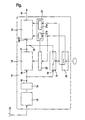
- an analog-to-digital converter 14 which is usually connected directly to a signal processor 15 (eg, a DSP, a "Digital Signal Processor") for filtering and analyzing the digitized receive signals 16.
- a signal processor 15 eg, a DSP, a "Digital Signal Processor"
- the measured values 17 obtained in this way can be sent directly to a computer-equipped computer Evaluation center transmitted or cached initially in the readout unit.
- serial-processing signal processor 15 is released from at least part of the tasks of analyzing and decoding the received signals 16 Algorithms in at least one acutely programmable (or already application-specific designed) complex logic device 18 (a FPGA ("Field Programmable Gate Array”) or an ASIC ("Application-Specific Integrated Circuit”)) are implemented, which is connected upstream of the signal processor 15 in series and only supplies further processed digital measured values 17 to the signal processor 15.
- a FPGA Field Programmable Gate Array
- ASIC Application-Specific Integrated Circuit
- the wireless receiver 11 may be equipped production side only earmarked at a designated slot with the logic module 18; or he is already pre-populated with it by default.
- the initially empty in the receiver circuit and now to be populated slot or the like recording or a standard therein already provided logic device 18 are now effectively effective by opening a bypass switch 19 in the signal path to the signal processor 15, as is apparent from the block diagram functionally.
- a switch 20 When running up to start of operation is specified via this switch 20, whether the radio receiver 11 now with increased detection reliability, ie with increased range, or whether he should be operated in power-saving mode. In the latter case, the switch 19 for bridging the installation position of a logic device 18 is closed and at the same time a nonvolatile configuration memory 21 a for programming the signal processor 15 activated in this mode in which he exercises within the function necessary at least rudimentary signal processing tasks from the functions of the logic device 18 ,
- the readout unit is raised with its radio receiver 11 in that functional position of the switch 20, in which the bypass switch 19 is opened, and thus an updatable configuration memory 22 for the logic device 18 is activated.
- a configuration memory 21 b is activated, which suppresses those functions in the signal processor 15, the logic block 18 which is now connected upstream of it are perceived; wherein the configuration functions 21a / 21b circuit technology can also be stored in a single, differentiated readable processor configuration memory 21.
- any future functional enhancements need not be intervened in the programming of the signal processor 15; they are more easily stored in the configuration memory 22 for the logic module 18.
- the signal processor 15 or its configuration memory 21 / 21a / 21b the logic module 18 or its configuration memory 22 configured itself, so that z. B. the signal processor 15 to be taken over by the logic device 18 functions - depending on programmed or entered specifications - yourself determined.
- the configuration memory 21 / 21a / 21b is integrated in the signal processor 15 and / or the configuration memory 22 in the logic module 18.
- the possibility is opened up to initialize a software radio receiver 11, as used in particular for obtaining digital measured values 17 via a signal processor 15 from demodulated and digitized data reception signals 16, optionally for operation in power-saving mode or for operation with increased range ,
- a substantial proportion of the detection algorithms is displaced into a logic module 18 connected upstream of the signal processor 15, the otherwise bridged function of which is released to some extent by activating its configuration memory 22 by opening a bridging switch 19.
Landscapes
- Engineering & Computer Science (AREA)
- Computer Networks & Wireless Communication (AREA)
- Signal Processing (AREA)
- Circuits Of Receivers In General (AREA)
- Noise Elimination (AREA)
Abstract
Description
- Die Erfindung betrifft einen Funkempfänger gemäß dem Oberbegriff des Hauptanspruchs, ein Verfahren zum Betreiben eines solchen Funkempfängers und eine Verwendung eines solchen Funkempfängers.
- Ein derartiger Funkempfänger ist etwa aus der
DE 10 2005 034 102 A1 zum Aufnehmen von Verbrauchswerten für die Abrechnung insbesondere von Wasser-, Wärme- oder Elektrizitätsverbrauch bekannt, ohne eigens ein Wohngebäude oder gar dessen einzelnen Wohnungen zum Ablesen von Mess-Stellen betreten zu müssen, weil deren aktuellen Messwerte über miniaturisierte Datensender ausgestrahlt werden. Diese messstellen-codierten Verbrauchswerte werden in einer den Funkempfänger enthaltenden Ausleseeinheit vorverarbeitet und gegebenenfalls zwischengespeichert sowie daraus an eine Abrechnungszentrale übermittelt. - Insbesondere Funkempfänger für Datenübermittlung werden zunehmend nicht mehr in Hardware, sondern in Software unter Berücksichtigung des vorbekannten Charakters der zu erwartenden, interessierenden Daten realisiert. Dafür wird das Antennen-Empfangssignal, gewöhnlich nach Vorverstärkung, mittels eines Scanprogrammes abgetastet und über angepasste Filteralgorithmen in einem Signalprozessor ausgewertet.
- In dem Zusammenhang soll nun die technische Problemstellung gelöst werden, die Performance im Sinne der allgemeinen Leistungsfähigkeit eines solchen Funkempfängers, unter Berücksichtigung auch von Aspekten möglichst geringen Leistungsbedarfes, zu erhöhen.
- Diese Aufgabe ist erfindungsgemäß durch die Merkmale des Hauptanspruchs gelöst. Danach können die digitalisierten Empfangssignale - statt unmittelbar - über einen programmierbaren digitalen Logikbaustein (ein FPGA ("Field Programmable Gate Array")) oder einen bereits anwendungsspezifisch ausgeführten digitalen Logikbaustein (einen ASIC ("Application-Specific Integrated Circuit")) auf einen Signalprozessor (einen DSP ("Digftal Signal Processor"), einen Mikrocontroller ("µC") oder einen Mikroprozessor) geschaltet werden. Aus der Aufnahme des Logikbausteins in der Empfängerschaltung vor dem Signalprozessor resultiert dann der Vorteil, zahlreiche Korrelations-, Filter- und Detektions-Algorithmen aus dem Prozessor heraus in diese Logikschaltung vorverlegen zu können, innerhalb derer Parallelverarbeitungen in Echtzeit ablaufen - im Gegensatz zur seriellen Signalverarbeitung in einem Prozessor. Solche Beschleunigung des Demodulierens von digitalen Daten schon vor der abschließenden Prozessorfunktion erlaubt praktisch ohne Zeitverlust die Anwendung von aufwändigeren Kriterien für eine kritischere Auswertung der Datensignale, und die wiederum führt zu einer Erhöhung der Detektionssicherheit, was wegen verbesserter Störresistenz eine größere nutzbare Empfangsreichweite zur Folge hat.
- Allerdings ist der Strombedarf derartiger Logikbausteine vergleichsweise hoch und insbesondere höher als bei einer reinen Prozessorverarbeitung. Deshalb ist gemäß der Erfindung weiterhin vorgesehen, den in Serie zum Signalprozessor liegenden Logikbaustein elektrisch zu überbrücken - oder gleich ganz fortzulassen -, nämlich wenn aufgrund der Umstände des zu erwartenden Einsatzszenarios solch eine erhöhte Performance des Daten-Funkempfängers gar nicht benötigt wird. Das kann etwa der Fall sein, wenn die Ausleseeinheit mit ihrem Empfänger im Stromsparmodus als Handgerät eingesetzt und in unmittelbarer Nähe von Datensendem vorbeigeführt werden soll. Wenn die Ausleseeinheit dagegen in einem Kraftfahrzeug betrieben wird, wo aus dem Bordnetz genügend Energie verfügbar ist, kann der Funkempfänger ohne weiteres mit dem Logikbaustein vor seinem Signalprozessor betrieben werden, um etwa von der Fahrbahn aus im Vorüberfahren auch über ein ausgedehntes Gelände verstreut betriebene Datensender im Weitbereichsmodus zu erfassen.
- Weitere Merkmale und zusätzliche Weiterbildungen der Erfindung ergeben sich aus den weiteren Ansprüchen und, auch hinsichtlich deren Vorteilen, aus nachstehender Beschreibung eines bevorzugten Realisierungsbeispieles zur erfindungsgemäßen Lösung. Die einzige Figur der Zeichnung veranschaulicht in der auf das Prinzipielle abstrahierten Skizze eines einpoligen Blockschaltbildes die Signalverarbeitung in einem erfindungsgemäß ausgelegten Daten-Funkempfänger.
- Ein derartiger, insbesondere in einer Messdaten-Ausleseeinheit betriebener Funkempfänger 11 ist mit einem Anschluss für eine interne oder externe Antenne 12 ausgestattet, die einen analogen Verstärker 13 speist. Dem folgt ein Analog-Digital-Wandler 14, Der ist gewöhnlich direkt auf einen Signalprozessor 15 (z. B. einen DSP, einen "Digital Signal Processor") zum Filtern und Analysieren der digitalisierten Empfangssignale 16 geschaltet. Die so gewonnen Messwerte 17 können unmittelbar an eine computerbestückte Auswertezentrale übermittelt oder zunächst in der Ausleseeinheit zwischengespeichert werden.
- Solche Signalverarbeitung lässt sich vertiefen und dennoch spürbar beschleunigen. Insbesondere lässt sich erfindungsgemäß ohne Verlängerung der Verarbeitungszeit über weitere Detektionskriterien eine gesteigerte Detektionszuverlässigkeit und folglich eine Erhöhung der Empfangsreichweite des Funkempfängers 11 erzielen, wenn der seriell arbeitende Signalprozessor 15 wenigstens von einem Teil der Aufgaben des Analysierens und Dekodierens der Empfangssignale 16 dadurch entbunden wird, dass deren Algorithmen in wenigstens einem akut programmierbaren (oder bereits anwendungsspezifisch ausgelegten) komplexen Logikbaustein 18 (einem FPGA ("Field Programmable Gate Array") oder einem ASIC ("Application-Specific Integrated Circuit")) implementiert werden, der dem Signalprozessor 15 in Serie vorgeschaltet wird und nur noch weiterzuverarbeitende digitale Messwerte 17 an den Signalprozessor 15 liefert. Dazu mag der Funkempfänger 11 fertigungsseitig erst zweckgebunden an einem dafür vorgesehenen Steckplatz mit dem Logikbaustein 18 bestückt werden; oder er ist damit bereits standardmäßig vorbestückt. Der in der Empfängerschaltung zunächst noch leere und nun zu bestückende Steckplatz oder dergleichen Aufnahme beziehungsweise ein darin schon standardmäßig vorgesehener Logikbaustein 18 werden nun gewissermaßen durch Öffnen eines Überbrückungs-Schalters 19 im Signalpfad zum Signalprozessor 15 wirksam, wie es sich aus dem Blockschaltbild funktional ergibt.
- Solche Auswahlmöglichkeit ist dort durch einen Umschalter 20 symbolisiert. Beim Hochlaufen zu Betriebsbeginn wird über diesen Umschalter 20 vorgegeben, ob der Funkempfänger 11 nun bei erhöhter Detektionszuverlässigkeit, also mit gesteigerter Reichweite, oder aber ob er im Stromsparmodus betrieben werden soll. In letzterem Falle wird der Schalter 19 zum Überbrücken der Einbauposition eines Logikbausteins 18 geschlossen und zugleich ein nichtflüchtiger Konfigurationsspeicher 21 a für die Programmierung des Signalprozessors 15 in dieser Betriebsart aktiviert, in der er im Rahmen des Funktionsnotwendigen wenigstens rudimentäre Signalverarbeitungsaufgaben aus den Funktionen des Logikbausteins 18 übemimmt.
- Wenn dagegen die Bestückung der Schaltung des Funkempfängers 11 unter Einschluss des gesonderten Logikbausteins 18 vor dem Signalprozessor 15 und deshalb mit gesteigerter Empfindlichkeit wirksam werden soll, dann wird die Ausleseeinheit mit ihrem Funkempfänger 11 in derjenigen Funktionsstellung des Umschalters 20 hochgefahren, in welcher der Überbrückungs-Schalter 19 geöffnet ist, und damit auch ein aktualisierbarer Konfigurationsspeicher 22 für den Logikbaustein 18 aktiviert. Zugleich wird ein Konfigurationsspeicher 21 b aktiviert, der im Signalprozessor 15 diejenigen Funktionen unterdrückt, die vom ihm nun vorgeschalteten Logikbaustein 18 wahrgenommen werden; wobei die Konfigurationsfunktionen 21a/21b schaltungstechnisch auch in einem einzigen, differenziert auslesbaren Prozessor-Konfigurationsspeicher 21 hinterlegt sein können. Für etwaige künftige Funktionserweiterungen braucht nicht in die Programmierung des Signalprozessors 15 eingegriffen zu werden; die werden einfacher im Konfigurationsspeicher 22 für den Logikbaustein 18 abgelegt.
- Daneben kann auch vorgesehen sein, dass der Signalprozessor 15 oder sein Konfigurationsspeicher 21/21a/21b den Logikbaustein 18 oder dessen Konfigurationsspeicher 22 selbst konfiguriert, dass also z. B. der Signalprozessor 15 die durch den Logikbaustein 18 zu übernehmenden Funktionen - je nach einprogrammierten oder eingegebenen Vorgaben - selbst bestimmt.
- Es sei noch erwähnt, dass in Ausgestaltung der Schaltung des Funkempfängers 11 natürlich ebenfalls vorgesehen sein kann, dass der Konfigurationsspeicher 21/21a/21b in den Signalprozessor 15 und/oder der Konfigurationsspeicher 22 in den Logikbaustein 18 integriert sind.
- So wird also erfindungsgemäß die Möglichkeit eröffnet, einen Software-Funkempfänger 11, wie er insbesondere zum Gewinnen digitaler Messwerte 17 über einen Signalprozessor 15 aus demodulierten und digitalisierten Daten-Empfangssignalen 16 Einsatz findet, wahlweise für Betrieb im Stromsparmodus oder für Betrieb mit gesteigerter Reichweite zu initialisieren. In letzterem Falle wird ein wesentlicher Anteil der Detektions-Algorithmen in einen dem Signalprozessor 15 vorgeschalteten Logikbaustein 18 verlagert, dessen ansonsten überbrückte Funktion dafür unter Aktivieren seines Konfigurationsspeichers 22 gewissermaßen durch Öffnen eines Überbrückungs-Schalters 19 freigegeben wird.
-
- 11
- Funkempfänger
- 12
- Antenne
- 13
- Verstärker (hinter 12)
- 14
- Analog-Digital-Wandler (ADC) (hinter 13)
- 15
- Signalprozessor (DSP)
- 16
- (digitalisierte) Empfangssignale (hinter 13)
- 17
- (digitale) Messwerte (hinter 15)
- 18
- digitaler Logikbaustein (FGPA /ASIC) (optional vor 15)
- 19
- Schalter (zum Überbrücken von 18)
- 20
- Umschalter
- 21
- Aktualisierbarer Konfigurationsspeicher (EPROM bzw. FLASH) (21 a+21 b für 15)
- 22
- Aktualisierbarer Konfigurationsspeicher (EPROM bzw. FLASH) (für 18)
Claims (13)
- Funkempfänger (11) mit Signalprozessor (15) zur Auswertung digitalisierter Empfangssignale (16), dadurch gekennzeichnet, dass der Funkempfänger zur überbrückbaren Aufnahme eines, programmierbaren oder anwendungsspezifisch ausgeführten, digitalen Logikbausteins (18) vor dem Signalprozessor (15) ausgelegt und mit der Funktion eines Umschalters (20) ausgestattet ist. dem gemäß eine Inbetriebnahme des Funkempfängers (11) entweder unter Überbrückung der Aufnahme für den Logikbaustein (18) oder aber unter Aktivieren eines Konfigurationsspeichers (22) für den Logikbaustein (18) initiierbar ist.
- Funkempfänger nach dem vorangehenden Anspruch, dadurch gekennzeichnet, dass bei Aktivieren des Konfigurationsspeichers (22) für den Logikbaustein (18) ein Konfigurationsspeicher (21 b) für den Signalprozessor (15) In diesem Funktionen sperrt, die vom Logikbaustein (18) übemommenen sind.
- Funkempfänger nach einem der vorangehenden Ansprüche, dadurch gekennzeichnet, dass in den Logikbaustein (18), im Interesse vergrößerter Empfangsreichweite, zusätzliche Algorithmen zur störungsresistenten Gewinnung von digitalen Daten aus den digitalisierten Empfangssignalen (16) implementiert sind.
- Funkempfänger nach einem der vorangehenden Ansprüche, dadurch gekennzeichnet, dass, im Interesse reduzierten Energieverbrauches, bei funktional zu überbrückendem Logikbaustein (18) ein Prozessor-Konfigurationsspeicher (21 a) aktivierbar ist, der im Signalprozessor (15) wenigstens die funktionswesentlichen Algorithmen für ein Umsetzen der digitalisierten Empfangssignale (16) in die digitalen Daten Implementiert.
- Funkempfänger nach einem der vorangehenden Ansprüche, dadurch gekennzeichnet, dass der Logikbaustein (18) und/oder sein Konfiguratiohsspeicher (22) von dem Signalprozessor (15) und/oder dessen Konfigurationsspeicher (21/21 a/21b) konfigurierbar ausgeführt sind.
- Funkempfänger nach einem der vorangehenden Ansprüche, dadurch gekennzeichnet, dass es sich bei den digitalen Daten um Messwerte (17) insbesondere für Verbrauchsabrechnungen handelt und der Funkempfänger zum Liefern der digitalen Messwerte (17) aus den digitalisierten Empfangssignalen (16) ausgebildet ist.
- Funkempfänger nach einem der vorangehenden Ansprüche, dadurch gekennzeichnet, dass es sich bei dem Logikbaustein (18) um ein FPGA oder einen ASIC und bei dem Signalprozessor (15) um einen DSP, einen Mikroprozessor oder einen Mikrocontroller handelt.
- Verfahren zum Betreiben eines Funkempfängers (11) nach einem der vorangehenden Ansprüche wahlweise in einem Weitbereichsmodus oder in einem Stromsparmodus durch Umschalten zwischen Freigeben und Überbrücken der Funktion eines, programmierbaren oder anwendungsspezifisch ausgeführten, digitalen Logikbausteins (18) vor dem Signalprozessor (15) zum Ausgeben digitaler Daten, insbesondere digitaler Messwerte (17) für Verbrauchsabrechnungen.
- Verfahren nach dem vorangehenden Anspruch, dadurch gekennzeichnet, dass bei Freigabe der Funktion des Logikbausteins (18) ein Konfigurationsspeicher (21b) für den Signalprozessor (15) in diesem Funktionen sperrt, die vom Logikbaustein (18) übernommenen werden.
- Verfahren nach Anspruch 8 oder 9, dadurch gekennzeichnet, dass der Logikbaustein (18), im Interesse vergrößerter Empfangsreichweite, zusätzliche Algorithmen zur störungsresistenten Gewinnung von digitalen Daten aus den digitalisierten Empfangssignalen (16) ausführt.
- Verfahren nach einem der Ansprüche 8 bis 10, dadurch gekennzeichnet, dass beim Initiieren des Funkempfängers (11) im Stromsparmodus ein Konfigurationsspeicher (21 a) zum Implementieren der funktionsnotwendigen Detektions-algorithmen des Logikbausteins (18) im Signalprozessor (15) aktiviert wird.
- Verfahren nach einem der Ansprüche 8 bis 11, dadurch gekennzeichnet, dass der Logikbaustein (18) und/oder sein Konfigurationsspeicher (22) von dem Signalprozessor (15) und/oder dessen Konfigurationsspeicher (21/21 a/21b) konfiguriert werden.
- Verwendung eines Funkempfängers (11) nach einem der Ansprüche 1 bis 7 zum Liefem von digitalen Messwerten (17) für Verbrauchsabrechnungen.
Applications Claiming Priority (1)
| Application Number | Priority Date | Filing Date | Title |
|---|---|---|---|
| DE102010056080A DE102010056080A1 (de) | 2010-12-23 | 2010-12-23 | Funkempfänger und Verfahren zu seinem Betrieb |
Publications (3)
| Publication Number | Publication Date |
|---|---|
| EP2469717A2 true EP2469717A2 (de) | 2012-06-27 |
| EP2469717A3 EP2469717A3 (de) | 2014-12-24 |
| EP2469717B1 EP2469717B1 (de) | 2017-06-21 |
Family
ID=45470178
Family Applications (1)
| Application Number | Title | Priority Date | Filing Date |
|---|---|---|---|
| EP11010036.9A Not-in-force EP2469717B1 (de) | 2010-12-23 | 2011-12-21 | Funkempfänger und Verfahren zu seinem Betrieb |
Country Status (2)
| Country | Link |
|---|---|
| EP (1) | EP2469717B1 (de) |
| DE (1) | DE102010056080A1 (de) |
Cited By (1)
| Publication number | Priority date | Publication date | Assignee | Title |
|---|---|---|---|---|
| WO2019166260A1 (de) * | 2018-02-28 | 2019-09-06 | Diehl Metering Systems Gmbh | Funkempfänger |
Citations (1)
| Publication number | Priority date | Publication date | Assignee | Title |
|---|---|---|---|---|
| DE102005034102A1 (de) | 2005-07-21 | 2007-02-01 | Hydrometer Gmbh | System zur Funkdatenübertragung |
Family Cites Families (4)
| Publication number | Priority date | Publication date | Assignee | Title |
|---|---|---|---|---|
| US6693953B2 (en) * | 1998-09-30 | 2004-02-17 | Skyworks Solutions, Inc. | Adaptive wireless communication receiver |
| WO2000069084A1 (en) * | 1999-05-07 | 2000-11-16 | Morphics Technology Inc. | Reprogrammable digital wireless communication device and method of operating same |
| US7272366B2 (en) * | 2001-12-17 | 2007-09-18 | Nokia Corporation | Method and apparatus for reducing RF filter induced distortion in a wide bandwidth wireless system by the use of channel-dependent RF filter compensation |
| US7856246B2 (en) * | 2007-03-21 | 2010-12-21 | Nokia Corporation | Multi-cell data processor |
-
2010
- 2010-12-23 DE DE102010056080A patent/DE102010056080A1/de not_active Withdrawn
-
2011
- 2011-12-21 EP EP11010036.9A patent/EP2469717B1/de not_active Not-in-force
Patent Citations (1)
| Publication number | Priority date | Publication date | Assignee | Title |
|---|---|---|---|---|
| DE102005034102A1 (de) | 2005-07-21 | 2007-02-01 | Hydrometer Gmbh | System zur Funkdatenübertragung |
Cited By (3)
| Publication number | Priority date | Publication date | Assignee | Title |
|---|---|---|---|---|
| WO2019166260A1 (de) * | 2018-02-28 | 2019-09-06 | Diehl Metering Systems Gmbh | Funkempfänger |
| CN111699631A (zh) * | 2018-02-28 | 2020-09-22 | 代傲表计系统有限公司 | 无线电接收器 |
| US11569855B2 (en) | 2018-02-28 | 2023-01-31 | Diehl Metering Systems Gmbh | Radio receiver and communications system |
Also Published As
| Publication number | Publication date |
|---|---|
| EP2469717B1 (de) | 2017-06-21 |
| DE102010056080A1 (de) | 2012-06-28 |
| EP2469717A3 (de) | 2014-12-24 |
Similar Documents
| Publication | Publication Date | Title |
|---|---|---|
| EP0492061B1 (de) | Fernbedienungssystem | |
| DE102012014471A1 (de) | Energieversorgungsschaltung für elektrische Komponenten | |
| EP3089263B1 (de) | Tragbare richtantenne, messanordnung und messverfahren | |
| DE102013200434A1 (de) | Vorrichtung und Verfahren zur Umfeldsensorik | |
| DE3706229C2 (de) | ||
| DE102015011930A1 (de) | Verfahren zum Betrieb eines Fahrerassistenzsystems zur Unterstützung von wenigstens einer Person außerhalb eines Kraftfahrzeugs | |
| DE102013106769B4 (de) | Fahrtenschreiber mit der Spurhalte- und Kollisionswarnfunktion | |
| DE102005046724A1 (de) | Fahrzeugseitige Fernbedienungseinheit | |
| DE102013206997A1 (de) | Überwachungssystem | |
| EP2469717B1 (de) | Funkempfänger und Verfahren zu seinem Betrieb | |
| EP2614869A1 (de) | Flüssigkeitsfilter | |
| DE102013220457A1 (de) | Sensoreinheit zum Bestimmen von Eigenschaften eines Schmiermittels sowie Maschinenelement und Maschinenanordnung | |
| DE102007029824B4 (de) | Vorrichtung zum Erfassen von Quadratursignalen | |
| DE102021001764A1 (de) | Bauteil für ein Fahrzeug mit einem Hohlraum und einem Feuchtesensor | |
| WO2021110715A1 (de) | Messen mit einem ultraschallsensorsystem in einer störumgebung | |
| DE10309600A1 (de) | Sicherungssystem | |
| EP2018578A1 (de) | Verfahren zur ortung von objekten mittels eines abbildenden radarsystems und transponder für die ortung von objekten mittels derartiger radarsysteme | |
| DE102006054317A1 (de) | Anordnung zur Erkennung einer Radbewegung | |
| WO2022083986A1 (de) | Anordnung für eine erfassung einer aktivierungshandlung und für eine kommunikation bei einem fahrzeug | |
| DE102013102613A1 (de) | Vorrichtung zum Stoppen eines in falscher Richtung fahrenden Kraftfahrzeugs und Batterie zur Verwendung bei einer derartigen Vorrichtung | |
| DE102005058144B4 (de) | Toröffnungssystem für ein Kraftfahrzeug | |
| DE102010056268A1 (de) | Verfahren zum gleichzeitigen Betreiben eines Störsenders sowie eines elektronischen Aufklärungssystems | |
| DE202017107396U1 (de) | Gebäude- oder Einfriedungsabschlussantriebsvorrichtung und System zum automatisierten Antreiben eines Gebäude- oder Einfriedungsabschlusses | |
| DE102016003845A1 (de) | Verfahren zur Warnung eines Fahrers eines Fahzeuges | |
| EP3057234A1 (de) | Sensoranordnung für ein kraftfahrzeug |
Legal Events
| Date | Code | Title | Description |
|---|---|---|---|
| AK | Designated contracting states |
Kind code of ref document: A2 Designated state(s): AL AT BE BG CH CY CZ DE DK EE ES FI FR GB GR HR HU IE IS IT LI LT LU LV MC MK MT NL NO PL PT RO RS SE SI SK SM TR |
|
| AX | Request for extension of the european patent |
Extension state: BA ME |
|
| PUAI | Public reference made under article 153(3) epc to a published international application that has entered the european phase |
Free format text: ORIGINAL CODE: 0009012 |
|
| RAP1 | Party data changed (applicant data changed or rights of an application transferred) |
Owner name: DIEHL METERING SYSTEMS GMBH Owner name: FRAUNHOFER-GESELLSCHAFT ZUR FOERDERUNG DER ANGEWAN |
|
| PUAL | Search report despatched |
Free format text: ORIGINAL CODE: 0009013 |
|
| AK | Designated contracting states |
Kind code of ref document: A3 Designated state(s): AL AT BE BG CH CY CZ DE DK EE ES FI FR GB GR HR HU IE IS IT LI LT LU LV MC MK MT NL NO PL PT RO RS SE SI SK SM TR |
|
| AX | Request for extension of the european patent |
Extension state: BA ME |
|
| RIC1 | Information provided on ipc code assigned before grant |
Ipc: H04B 1/16 20060101AFI20141118BHEP Ipc: H04W 52/02 20090101ALN20141118BHEP |
|
| 17P | Request for examination filed |
Effective date: 20150622 |
|
| RBV | Designated contracting states (corrected) |
Designated state(s): AL AT BE BG CH CY CZ DE DK EE ES FI FR GB GR HR HU IE IS IT LI LT LU LV MC MK MT NL NO PL PT RO RS SE SI SK SM TR |
|
| 17Q | First examination report despatched |
Effective date: 20161006 |
|
| STAA | Information on the status of an ep patent application or granted ep patent |
Free format text: STATUS: EXAMINATION IS IN PROGRESS |
|
| GRAP | Despatch of communication of intention to grant a patent |
Free format text: ORIGINAL CODE: EPIDOSNIGR1 |
|
| STAA | Information on the status of an ep patent application or granted ep patent |
Free format text: STATUS: GRANT OF PATENT IS INTENDED |
|
| INTG | Intention to grant announced |
Effective date: 20170314 |
|
| GRAS | Grant fee paid |
Free format text: ORIGINAL CODE: EPIDOSNIGR3 |
|
| GRAA | (expected) grant |
Free format text: ORIGINAL CODE: 0009210 |
|
| STAA | Information on the status of an ep patent application or granted ep patent |
Free format text: STATUS: THE PATENT HAS BEEN GRANTED |
|
| AK | Designated contracting states |
Kind code of ref document: B1 Designated state(s): AL AT BE BG CH CY CZ DE DK EE ES FI FR GB GR HR HU IE IS IT LI LT LU LV MC MK MT NL NO PL PT RO RS SE SI SK SM TR |
|
| REG | Reference to a national code |
Ref country code: GB Ref legal event code: FG4D Free format text: NOT ENGLISH |
|
| REG | Reference to a national code |
Ref country code: CH Ref legal event code: EP |
|
| REG | Reference to a national code |
Ref country code: IE Ref legal event code: FG4D Free format text: LANGUAGE OF EP DOCUMENT: GERMAN |
|
| REG | Reference to a national code |
Ref country code: AT Ref legal event code: REF Ref document number: 903777 Country of ref document: AT Kind code of ref document: T Effective date: 20170715 |
|
| REG | Reference to a national code |
Ref country code: DE Ref legal event code: R096 Ref document number: 502011012467 Country of ref document: DE |
|
| REG | Reference to a national code |
Ref country code: NL Ref legal event code: MP Effective date: 20170621 |
|
| PG25 | Lapsed in a contracting state [announced via postgrant information from national office to epo] |
Ref country code: HR Free format text: LAPSE BECAUSE OF FAILURE TO SUBMIT A TRANSLATION OF THE DESCRIPTION OR TO PAY THE FEE WITHIN THE PRESCRIBED TIME-LIMIT Effective date: 20170621 Ref country code: FI Free format text: LAPSE BECAUSE OF FAILURE TO SUBMIT A TRANSLATION OF THE DESCRIPTION OR TO PAY THE FEE WITHIN THE PRESCRIBED TIME-LIMIT Effective date: 20170621 Ref country code: NO Free format text: LAPSE BECAUSE OF FAILURE TO SUBMIT A TRANSLATION OF THE DESCRIPTION OR TO PAY THE FEE WITHIN THE PRESCRIBED TIME-LIMIT Effective date: 20170921 Ref country code: GR Free format text: LAPSE BECAUSE OF FAILURE TO SUBMIT A TRANSLATION OF THE DESCRIPTION OR TO PAY THE FEE WITHIN THE PRESCRIBED TIME-LIMIT Effective date: 20170922 Ref country code: LT Free format text: LAPSE BECAUSE OF FAILURE TO SUBMIT A TRANSLATION OF THE DESCRIPTION OR TO PAY THE FEE WITHIN THE PRESCRIBED TIME-LIMIT Effective date: 20170621 |
|
| REG | Reference to a national code |
Ref country code: LT Ref legal event code: MG4D |
|
| PG25 | Lapsed in a contracting state [announced via postgrant information from national office to epo] |
Ref country code: NL Free format text: LAPSE BECAUSE OF FAILURE TO SUBMIT A TRANSLATION OF THE DESCRIPTION OR TO PAY THE FEE WITHIN THE PRESCRIBED TIME-LIMIT Effective date: 20170621 Ref country code: RS Free format text: LAPSE BECAUSE OF FAILURE TO SUBMIT A TRANSLATION OF THE DESCRIPTION OR TO PAY THE FEE WITHIN THE PRESCRIBED TIME-LIMIT Effective date: 20170621 Ref country code: BG Free format text: LAPSE BECAUSE OF FAILURE TO SUBMIT A TRANSLATION OF THE DESCRIPTION OR TO PAY THE FEE WITHIN THE PRESCRIBED TIME-LIMIT Effective date: 20170921 Ref country code: LV Free format text: LAPSE BECAUSE OF FAILURE TO SUBMIT A TRANSLATION OF THE DESCRIPTION OR TO PAY THE FEE WITHIN THE PRESCRIBED TIME-LIMIT Effective date: 20170621 Ref country code: SE Free format text: LAPSE BECAUSE OF FAILURE TO SUBMIT A TRANSLATION OF THE DESCRIPTION OR TO PAY THE FEE WITHIN THE PRESCRIBED TIME-LIMIT Effective date: 20170621 |
|
| REG | Reference to a national code |
Ref country code: FR Ref legal event code: PLFP Year of fee payment: 7 |
|
| PG25 | Lapsed in a contracting state [announced via postgrant information from national office to epo] |
Ref country code: RO Free format text: LAPSE BECAUSE OF FAILURE TO SUBMIT A TRANSLATION OF THE DESCRIPTION OR TO PAY THE FEE WITHIN THE PRESCRIBED TIME-LIMIT Effective date: 20170621 Ref country code: EE Free format text: LAPSE BECAUSE OF FAILURE TO SUBMIT A TRANSLATION OF THE DESCRIPTION OR TO PAY THE FEE WITHIN THE PRESCRIBED TIME-LIMIT Effective date: 20170621 Ref country code: SK Free format text: LAPSE BECAUSE OF FAILURE TO SUBMIT A TRANSLATION OF THE DESCRIPTION OR TO PAY THE FEE WITHIN THE PRESCRIBED TIME-LIMIT Effective date: 20170621 Ref country code: CZ Free format text: LAPSE BECAUSE OF FAILURE TO SUBMIT A TRANSLATION OF THE DESCRIPTION OR TO PAY THE FEE WITHIN THE PRESCRIBED TIME-LIMIT Effective date: 20170621 |
|
| PG25 | Lapsed in a contracting state [announced via postgrant information from national office to epo] |
Ref country code: IT Free format text: LAPSE BECAUSE OF FAILURE TO SUBMIT A TRANSLATION OF THE DESCRIPTION OR TO PAY THE FEE WITHIN THE PRESCRIBED TIME-LIMIT Effective date: 20170621 Ref country code: IS Free format text: LAPSE BECAUSE OF FAILURE TO SUBMIT A TRANSLATION OF THE DESCRIPTION OR TO PAY THE FEE WITHIN THE PRESCRIBED TIME-LIMIT Effective date: 20171021 Ref country code: SM Free format text: LAPSE BECAUSE OF FAILURE TO SUBMIT A TRANSLATION OF THE DESCRIPTION OR TO PAY THE FEE WITHIN THE PRESCRIBED TIME-LIMIT Effective date: 20170621 Ref country code: ES Free format text: LAPSE BECAUSE OF FAILURE TO SUBMIT A TRANSLATION OF THE DESCRIPTION OR TO PAY THE FEE WITHIN THE PRESCRIBED TIME-LIMIT Effective date: 20170621 Ref country code: PL Free format text: LAPSE BECAUSE OF FAILURE TO SUBMIT A TRANSLATION OF THE DESCRIPTION OR TO PAY THE FEE WITHIN THE PRESCRIBED TIME-LIMIT Effective date: 20170621 |
|
| REG | Reference to a national code |
Ref country code: DE Ref legal event code: R097 Ref document number: 502011012467 Country of ref document: DE |
|
| PLBE | No opposition filed within time limit |
Free format text: ORIGINAL CODE: 0009261 |
|
| STAA | Information on the status of an ep patent application or granted ep patent |
Free format text: STATUS: NO OPPOSITION FILED WITHIN TIME LIMIT |
|
| PG25 | Lapsed in a contracting state [announced via postgrant information from national office to epo] |
Ref country code: DK Free format text: LAPSE BECAUSE OF FAILURE TO SUBMIT A TRANSLATION OF THE DESCRIPTION OR TO PAY THE FEE WITHIN THE PRESCRIBED TIME-LIMIT Effective date: 20170621 |
|
| 26N | No opposition filed |
Effective date: 20180322 |
|
| REG | Reference to a national code |
Ref country code: CH Ref legal event code: PL |
|
| PG25 | Lapsed in a contracting state [announced via postgrant information from national office to epo] |
Ref country code: SI Free format text: LAPSE BECAUSE OF FAILURE TO SUBMIT A TRANSLATION OF THE DESCRIPTION OR TO PAY THE FEE WITHIN THE PRESCRIBED TIME-LIMIT Effective date: 20170621 |
|
| REG | Reference to a national code |
Ref country code: IE Ref legal event code: MM4A |
|
| PG25 | Lapsed in a contracting state [announced via postgrant information from national office to epo] |
Ref country code: MT Free format text: LAPSE BECAUSE OF FAILURE TO SUBMIT A TRANSLATION OF THE DESCRIPTION OR TO PAY THE FEE WITHIN THE PRESCRIBED TIME-LIMIT Effective date: 20170621 Ref country code: LU Free format text: LAPSE BECAUSE OF NON-PAYMENT OF DUE FEES Effective date: 20171221 |
|
| REG | Reference to a national code |
Ref country code: BE Ref legal event code: MM Effective date: 20171231 |
|
| PG25 | Lapsed in a contracting state [announced via postgrant information from national office to epo] |
Ref country code: IE Free format text: LAPSE BECAUSE OF NON-PAYMENT OF DUE FEES Effective date: 20171221 |
|
| PG25 | Lapsed in a contracting state [announced via postgrant information from national office to epo] |
Ref country code: BE Free format text: LAPSE BECAUSE OF NON-PAYMENT OF DUE FEES Effective date: 20171231 Ref country code: LI Free format text: LAPSE BECAUSE OF NON-PAYMENT OF DUE FEES Effective date: 20171231 Ref country code: CH Free format text: LAPSE BECAUSE OF NON-PAYMENT OF DUE FEES Effective date: 20171231 |
|
| REG | Reference to a national code |
Ref country code: AT Ref legal event code: MM01 Ref document number: 903777 Country of ref document: AT Kind code of ref document: T Effective date: 20171221 |
|
| PGFP | Annual fee paid to national office [announced via postgrant information from national office to epo] |
Ref country code: GB Payment date: 20181218 Year of fee payment: 8 Ref country code: FR Payment date: 20181220 Year of fee payment: 8 |
|
| PG25 | Lapsed in a contracting state [announced via postgrant information from national office to epo] |
Ref country code: AT Free format text: LAPSE BECAUSE OF NON-PAYMENT OF DUE FEES Effective date: 20171221 |
|
| PGFP | Annual fee paid to national office [announced via postgrant information from national office to epo] |
Ref country code: DE Payment date: 20190213 Year of fee payment: 8 |
|
| PG25 | Lapsed in a contracting state [announced via postgrant information from national office to epo] |
Ref country code: MC Free format text: LAPSE BECAUSE OF FAILURE TO SUBMIT A TRANSLATION OF THE DESCRIPTION OR TO PAY THE FEE WITHIN THE PRESCRIBED TIME-LIMIT Effective date: 20170621 Ref country code: HU Free format text: LAPSE BECAUSE OF FAILURE TO SUBMIT A TRANSLATION OF THE DESCRIPTION OR TO PAY THE FEE WITHIN THE PRESCRIBED TIME-LIMIT; INVALID AB INITIO Effective date: 20111221 |
|
| PG25 | Lapsed in a contracting state [announced via postgrant information from national office to epo] |
Ref country code: CY Free format text: LAPSE BECAUSE OF NON-PAYMENT OF DUE FEES Effective date: 20170621 |
|
| PG25 | Lapsed in a contracting state [announced via postgrant information from national office to epo] |
Ref country code: MK Free format text: LAPSE BECAUSE OF FAILURE TO SUBMIT A TRANSLATION OF THE DESCRIPTION OR TO PAY THE FEE WITHIN THE PRESCRIBED TIME-LIMIT Effective date: 20170621 |
|
| PG25 | Lapsed in a contracting state [announced via postgrant information from national office to epo] |
Ref country code: TR Free format text: LAPSE BECAUSE OF FAILURE TO SUBMIT A TRANSLATION OF THE DESCRIPTION OR TO PAY THE FEE WITHIN THE PRESCRIBED TIME-LIMIT Effective date: 20170621 |
|
| PG25 | Lapsed in a contracting state [announced via postgrant information from national office to epo] |
Ref country code: PT Free format text: LAPSE BECAUSE OF FAILURE TO SUBMIT A TRANSLATION OF THE DESCRIPTION OR TO PAY THE FEE WITHIN THE PRESCRIBED TIME-LIMIT Effective date: 20170621 |
|
| REG | Reference to a national code |
Ref country code: DE Ref legal event code: R119 Ref document number: 502011012467 Country of ref document: DE |
|
| PG25 | Lapsed in a contracting state [announced via postgrant information from national office to epo] |
Ref country code: AL Free format text: LAPSE BECAUSE OF FAILURE TO SUBMIT A TRANSLATION OF THE DESCRIPTION OR TO PAY THE FEE WITHIN THE PRESCRIBED TIME-LIMIT Effective date: 20170621 |
|
| GBPC | Gb: european patent ceased through non-payment of renewal fee |
Effective date: 20191221 |
|
| PG25 | Lapsed in a contracting state [announced via postgrant information from national office to epo] |
Ref country code: FR Free format text: LAPSE BECAUSE OF NON-PAYMENT OF DUE FEES Effective date: 20191231 Ref country code: DE Free format text: LAPSE BECAUSE OF NON-PAYMENT OF DUE FEES Effective date: 20200701 Ref country code: GB Free format text: LAPSE BECAUSE OF NON-PAYMENT OF DUE FEES Effective date: 20191221 |