EP2469709A2 - Composite substrate and method for manufacturing the composite substrate - Google Patents
Composite substrate and method for manufacturing the composite substrate Download PDFInfo
- Publication number
- EP2469709A2 EP2469709A2 EP20110194768 EP11194768A EP2469709A2 EP 2469709 A2 EP2469709 A2 EP 2469709A2 EP 20110194768 EP20110194768 EP 20110194768 EP 11194768 A EP11194768 A EP 11194768A EP 2469709 A2 EP2469709 A2 EP 2469709A2
- Authority
- EP
- European Patent Office
- Prior art keywords
- substrate
- piezoelectric substrate
- adhesive layer
- bonded
- piezoelectric
- Prior art date
- Legal status (The legal status is an assumption and is not a legal conclusion. Google has not performed a legal analysis and makes no representation as to the accuracy of the status listed.)
- Granted
Links
Images


Classifications
-
- H—ELECTRICITY
- H03—ELECTRONIC CIRCUITRY
- H03H—IMPEDANCE NETWORKS, e.g. RESONANT CIRCUITS; RESONATORS
- H03H9/00—Networks comprising electromechanical or electro-acoustic elements; Electromechanical resonators
- H03H9/15—Constructional features of resonators consisting of piezoelectric or electrostrictive material
-
- H—ELECTRICITY
- H03—ELECTRONIC CIRCUITRY
- H03H—IMPEDANCE NETWORKS, e.g. RESONANT CIRCUITS; RESONATORS
- H03H9/00—Networks comprising electromechanical or electro-acoustic elements; Electromechanical resonators
- H03H9/02—Details
- H03H9/02535—Details of surface acoustic wave devices
- H03H9/02543—Characteristics of substrate, e.g. cutting angles
- H03H9/02574—Characteristics of substrate, e.g. cutting angles of combined substrates, multilayered substrates, piezoelectrical layers on not-piezoelectrical substrate
-
- H—ELECTRICITY
- H03—ELECTRONIC CIRCUITRY
- H03H—IMPEDANCE NETWORKS, e.g. RESONANT CIRCUITS; RESONATORS
- H03H3/00—Apparatus or processes specially adapted for the manufacture of impedance networks, resonating circuits, resonators
- H03H3/007—Apparatus or processes specially adapted for the manufacture of impedance networks, resonating circuits, resonators for the manufacture of electromechanical resonators or networks
- H03H3/02—Apparatus or processes specially adapted for the manufacture of impedance networks, resonating circuits, resonators for the manufacture of electromechanical resonators or networks for the manufacture of piezoelectric or electrostrictive resonators or networks
-
- H—ELECTRICITY
- H03—ELECTRONIC CIRCUITRY
- H03H—IMPEDANCE NETWORKS, e.g. RESONANT CIRCUITS; RESONATORS
- H03H3/00—Apparatus or processes specially adapted for the manufacture of impedance networks, resonating circuits, resonators
- H03H3/007—Apparatus or processes specially adapted for the manufacture of impedance networks, resonating circuits, resonators for the manufacture of electromechanical resonators or networks
- H03H3/08—Apparatus or processes specially adapted for the manufacture of impedance networks, resonating circuits, resonators for the manufacture of electromechanical resonators or networks for the manufacture of resonators or networks using surface acoustic waves
-
- H—ELECTRICITY
- H03—ELECTRONIC CIRCUITRY
- H03H—IMPEDANCE NETWORKS, e.g. RESONANT CIRCUITS; RESONATORS
- H03H9/00—Networks comprising electromechanical or electro-acoustic elements; Electromechanical resonators
- H03H9/02—Details
- H03H9/02007—Details of bulk acoustic wave devices
- H03H9/02015—Characteristics of piezoelectric layers, e.g. cutting angles
-
- H—ELECTRICITY
- H10—SEMICONDUCTOR DEVICES; ELECTRIC SOLID-STATE DEVICES NOT OTHERWISE PROVIDED FOR
- H10N—ELECTRIC SOLID-STATE DEVICES NOT OTHERWISE PROVIDED FOR
- H10N30/00—Piezoelectric or electrostrictive devices
- H10N30/01—Manufacture or treatment
- H10N30/07—Forming of piezoelectric or electrostrictive parts or bodies on an electrical element or another base
- H10N30/072—Forming of piezoelectric or electrostrictive parts or bodies on an electrical element or another base by laminating or bonding of piezoelectric or electrostrictive bodies
- H10N30/073—Forming of piezoelectric or electrostrictive parts or bodies on an electrical element or another base by laminating or bonding of piezoelectric or electrostrictive bodies by fusion of metals or by adhesives
-
- H—ELECTRICITY
- H10—SEMICONDUCTOR DEVICES; ELECTRIC SOLID-STATE DEVICES NOT OTHERWISE PROVIDED FOR
- H10N—ELECTRIC SOLID-STATE DEVICES NOT OTHERWISE PROVIDED FOR
- H10N30/00—Piezoelectric or electrostrictive devices
- H10N30/01—Manufacture or treatment
- H10N30/08—Shaping or machining of piezoelectric or electrostrictive bodies
- H10N30/085—Shaping or machining of piezoelectric or electrostrictive bodies by machining
- H10N30/086—Shaping or machining of piezoelectric or electrostrictive bodies by machining by polishing or grinding
-
- Y—GENERAL TAGGING OF NEW TECHNOLOGICAL DEVELOPMENTS; GENERAL TAGGING OF CROSS-SECTIONAL TECHNOLOGIES SPANNING OVER SEVERAL SECTIONS OF THE IPC; TECHNICAL SUBJECTS COVERED BY FORMER USPC CROSS-REFERENCE ART COLLECTIONS [XRACs] AND DIGESTS
- Y10—TECHNICAL SUBJECTS COVERED BY FORMER USPC
- Y10T—TECHNICAL SUBJECTS COVERED BY FORMER US CLASSIFICATION
- Y10T29/00—Metal working
- Y10T29/42—Piezoelectric device making
Definitions
- the present invention relates to a composite substrate and a method for manufacturing the composite substrate.
- Patent Document 1 discloses a composite substrate including a piezoelectric substrate formed of lithium niobate, lithium tantalate, or the like and a support substrate formed of silicon, quartz, or the like. According to Patent Document 1, the piezoelectric substrate and the support substrate are bonded together by applying an ultraviolet-curable adhesive to the support substrate by spin coating.
- Patent Document 1 JP 2006-319679 A
- the adhesive When the adhesive is applied to the support substrate by spin coating, the adhesive forms a swelling portion in an outer peripheral area thereof, owing to a centrifugal force applied in the spin coating process.
- adhesion failure may occur at the swelling portion.
- the support substrate and the piezoelectric substrate may become separated from each other. Such a separation probably occurs because of air bubbles that enter between the swelling portion of the adhesive layer and the piezoelectric substrate.
- the present invention has been made in view of the above-described problem, and the main object of the present invention is to reliably bond a support substrate and a piezoelectric substrate to each other with an adhesive layer including a swelling portion in an outer peripheral area thereof.
- a composite substrate according to the present invention includes a piezoelectric substrate, a support substrate, and an adhesive layer with which the piezoelectric substrate and the support substrate are bonded to each other.
- the adhesive layer includes a flat portion and a swelling portion formed in an outer peripheral area of the flat portion.
- the piezoelectric substrate includes a first surface that is bonded to the flat portion of the adhesive layer and a second surface at the side opposite to the front surface, and is bonded to the support substrate in an area excluding the swelling portion.
- the adhesive layer in the composite substrate includes the swelling portion in the outer peripheral area thereof
- the piezoelectric substrate is bonded to the support substrate in the area excluding the swelling portion. Accordingly, air bubbles do not easily enter between the swelling portion of the adhesive layer and the piezoelectric substrate, and separations caused by the air bubbles can be prevented. As a result, the support substrate and the piezoelectric substrate can be reliably bonded to each other with the adhesive layer including the swelling portion in the outer peripheral area thereof.
- an outer peripheral edge of the first surface may be in contact with a boundary between the swelling portion and the flat portion of the adhesive layer.
- the edge portion of of the first surface as the bonding area between the piezoelectric substrate and the adhesive layer is protected by the swelling portion of the adhesive layer. Accordingly, when the composite substrate is subjected to a cleaning process, the piezoelectric substrate may be prevented from being separated from the adhesive layer by acid or alkaline solution used in the cleaning process.
- the piezoelectric substrate may have a bulging portion that is formed such that the first surface of the piezoelectric substrate is inside the second surface of the piezoelectric substrate when the first surface is projected in a perpendicular direction onto the second surface.
- cracks can be prevented from being formed in the piezoelectric substrate when, for example, the composite substrate is subjected to a heating process.
- the reason for this is believed to be as follows. That is, since the piezoelectric substrate includes the bulging portion, the second surface of the piezoelectric substrate that is not bonded to the support substrate is larger than the first surface of the piezoelectric substrate that is bonded to the support substrate with the adhesive layer.
- the volume of the second surface which has more freedom than the first surface, is relatively large.
- the bulging portion probably serves to reduce the stress applied to the edge portion when the support substrate and the piezoelectric substrate expand or contract in the heating process.
- an angle between the first surface of the piezoelectric substrate and an outer peripheral surface of the piezoelectric substrate may be obtuse.
- a method for manufacturing a composite substrate according to the present invention includes (a) a step of preparing a piezoelectric substrate; (b) a step of applying an adhesive to a surface of a support substrate by spin coating; and (c) a step of forming a composite substrate by bonding the support substrate and the piezoelectric substrate to each other with the adhesive.
- the piezoelectric substrate prepared in step (a) includes a first surface and is shaped such that, in bonding in step (c), the first surface of the piezoelectric substrate is capable of being bonded to a flat portion of the adhesive layer and the piezoelectric substrate is capable of being bonded to the support substrate in an area excluding a swelling portion of the adhesive layer that is formed in an outer peripheral area of the flat portion, the flat portion and the swelling portion being formed when the adhesive is applied to the support substrate by spin coating in step (b).
- step (c) the bonding is performed so that the first surface is bonded to the flat surface of the adhesive layer and that the piezoelectric substrate is bonded to the support substrate in the area excluding the swelling portion
- the piezoelectric substrate is bonded to the support substrate in the area excluding the swelling portion in step (c). Accordingly, air bubbles do not easily enter between the swelling portion of the adhesive layer and the piezoelectric substrate, and separations caused by the air bubbles can be prevented in the composite substrate manufactured by the above-described manufacturing method. As a result, a composite substrate may be manufactured in which the support substrate and the piezoelectric substrate are reliably bonded to each other with the adhesive layer including the swelling portion in the outer peripheral area thereof.
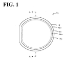
- Fig. 1 is a plan view of a composite substrate 10 according to an embodiment of the present invention.
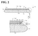
- Fig. 2 is a sectional view of Fig. 1 taken along line A-A.
- the composite substrate 10 according to the present invention is formed by bonding a plurality of substrates together.
- the composite substrate 10 includes a support substrate 12, a piezoelectric substrate 14, and an adhesive layer 16 with which a front surface 12a of the support substrate 12 and a back surface 14b of the piezoelectric substrate 14 are bonded to each other.
- the composite substrate 10 has a circular shape with a single flat portion. This flat portion is called an orientation flat (OF) portion, and is used to detect the position and orientation of a wafer when, for example, the wafer is subjected to various operations in a process of manufacturing a surface acoustic wave device.
- OF orientation flat
- the support substrate 12 supports the piezoelectric substrate 14 that is bonded to the front surface 12a, which is the top surface of the support substrate 12, with the adhesive layer 16.
- the material of the support substrate 12 may be, for example, silicon, sapphire, aluminum nitride, alumina, borosilicate glass, silica glass, lithium tantalate, lithium niobate, lithium niobate-lithium tantalate solid-solution single crystal, lithium borate, langasite, or quartz.
- the support substrate 12 has a coefficient of thermal expansion that is lower than that of the piezoelectric substrate 14. The difference in coefficient of thermal expansion between the support substrate 12 and the piezoelectric substrate 14 may be 5 ppm/°C or more.
- the coefficient of thermal expansion of the piezoelectric substrate 14 is in the range of 13 to 20 ppm/°C
- the coefficient of thermal expansion of the support substrate 12 is preferably in the range of 2 to 7 ppm/°C.
- the size of the support substrate 12 is not particularly limited.
- the support substrate 12 may have a diameter in the range of 50 to 150 mm and a thickness in the range of 100 to 500 ⁇ m.
- the front surface 12a is a bonding surface of the support substrate 12 that is bonded to the adhesive layer 16.
- the term "front surface” is used merely for convenience, and the front surface may instead be referred to as a "back surface".
- the adhesive layer 16 is provided to bond the front surface 12a of the support substrate 12 and the back surface 14b of the piezoelectric substrate 14 to each other.
- the adhesive layer 16 includes a swelling portion 16a in an outer peripheral area thereof.
- the swelling portion 16a is formed when, for example, an adhesive is applied to the front surface 12a of the support substrate 12 by spin coating to form the adhesive layer 16.
- a portion of the adhesive layer 16 other than the swelling portion 16a is formed as a flat portion 16b. Namely, the adhesive layer 16 includes the swelling portion 16a and the flat portion 16b.
- a heat-resistant organic adhesive is preferably used.
- an epoxy adhesive or an acrylic adhesive may be used.
- the piezoelectric substrate 14 is a substrate capable of propagating acoustic waves (in particular, surface acoustic waves).
- the material of the piezoelectric substrate 14 may be, for example, lithium tantalate, lithium niobate, lithium niobate-lithium tantalate solid-solution single crystal, lithium borate, langasite, or quartz.
- the back surface 14b (a first surface) of the piezoelectric substrate 14 is in contact with the flat portion 16b of the adhesive layer 16, but is not in contact with the swelling portion 16a.
- the piezoelectric substrate 14 is bonded to the support substrate 12 with the adhesive layer 16 in an area excluding the swelling portion 16a of the adhesive layer 16.
- the piezoelectric substrate 14 includes a bulging portion 14d that is formed such that the back surface 14b is inside a front surface 14a (a second surface) when the back surface 14b is projected onto the front surface 14a in a direction perpendicular to the front surface 14a.
- an outer peripheral surface 14e of the piezoelectric substrate 14 is formed such that the circumference thereof increases toward the front surface 14a from the back surface 14b.
- the outer peripheral surface 14e is formed such that an angle ⁇ between the back surface 14b and the outer peripheral surface 14e is more than 90° and less than 180°, that is, such that the angle ⁇ is obtuse.
- the angle ⁇ is preferably in the range of 110° or more and 170° or less.
- the back surface 14b is a bonding surface of the piezoelectric substrate 14 that is bonded to the adhesive layer 16, and the front surface 14a is a surface at the side opposite to the bonding surface (back surface 14b).
- the terms "front surface” and "back surface” are used merely for convenience.
- the bonding surface (the first surface) of the piezoelectric substrate 14 that is bonded to the adhesive layer 16 may instead be referred to as a "front surface", and the surface (the second surface) at the side opposite to the bonding surface may instead be referred to as a "back surface”.
- acoustic wave devices are formed on the composite substrate 10 by photolithography, and then the individual acoustic wave devices are separated from each other by a dicing process.
- the acoustic wave devices may be, for example, surface acoustic wave devices, Lamb wave devices, or film bulk acoustic resonators (FBAR).
- FBAR film bulk acoustic resonators
- a surface acoustic wave device is formed by arranging an input interdigital transducer (IDT) electrode (also referred to as a comb-shaped electrode or an interdigital transducer) for exciting a surface acoustic wave and an output IDT electrode that receives the surface acoustic wave on the front surface 14a of the piezoelectric substrate 14.
- IDT input interdigital transducer
- the support substrate 12 has a coefficient of thermal expansion that is lower than that of the piezoelectric substrate 14. Therefore, in a surface acoustic wave device that is formed by using the composite substrate 10, variation in the size of the piezoelectric substrate 14 caused by temperature variation can be suppressed by the support substrate 12. As a result, variation in frequency characteristics of the surface acoustic wave device caused by temperature variation can be suppressed.
- Figs. 3A to 3D are schematic sectional views illustrating a manufacturing process of the composite substrate 10.
- the method for manufacturing the composite substrate 10 includes (a) a step of preparing a piezoelectric substrate 24 having an outer peripheral surface that has been ground; (b) a step of applying an adhesive by spin coating to the front surface 12a of the support substrate 12 that has been prepared; and (c) a step of forming a composite substrate 20 by bonding the front surface 12a of the support substrate 12 and a back surface 24b of the piezoelectric substrate 24 to each other with the adhesive.
- the piezoelectric substrate 24, which is used to form the piezoelectric substrate 14, is prepared ( Fig. 3A ).
- the piezoelectric substrate 24 may be made of one of the above-mentioned materials.
- the size of the piezoelectric substrate 24 is not particularly limited.
- the piezoelectric substrate 24 may have a diameter in the range of 50 to 150 mm and a thickness in the range of 250 to 500 ⁇ m.
- An outer peripheral portion (portion shown by broken lines in Fig. 3A ) of the piezoelectric substrate 24 is ground in advance so that the angle between the back surface 24b and an outer peripheral surface 24e after the grinding process is set to ⁇ . The value of the angle ⁇ will be described below.
- a substrate that is initially formed in the shape shown by the solid lines in Fig. 3A may be prepared as the piezoelectric substrate 24.
- step (b) the support substrate 12 is prepared and an adhesive 26 used to form the adhesive layer 16 is applied to the front surface 12a of the support substrate 12 (see Fig. 3B ).
- the support substrate 12 may be made of one of the above-mentioned materials and have the above-described size.
- the adhesive 26 may be one of the above-mentioned materials of the adhesive layer 16.
- the adhesive 26 forms a swelling portion 26a in an outer peripheral area thereof and a flat portion 26b in an area other than the swelling portion 26a.
- step (c) the composite substrate 20 is formed by bonding the front surface 12a of the support substrate 12 and the back surface 24b of the piezoelectric substrate 24 to each other with the adhesive 26 and solidifying the adhesive 26 ( Fig. 3C ).
- the adhesive 26 is formed into the adhesive layer 16 by the solidifying process.
- the piezoelectric substrate 24 prepared in step (a) is shaped such that, in step (c), the piezoelectric substrate 24 is bonded with the adhesive 26 in an area excluding the swelling portion 26a and an outer peripheral edge 24c of the back surface 24b comes into contact with a boundary 26c between the swelling portion 26a and the flat portion 26b of the adhesive 26.
- the back surface 24b of the piezoelectric substrate 24 is not bonded to the swelling portion 16a.
- the angle ⁇ of the piezoelectric substrate 24 prepared in step (a) is set in advance such that the piezoelectric substrate 24 can be bonded in the above-described manner.
- the size of the swelling portion 26a is determined by the diameter of the support substrate 12, the material of the adhesive 26, and conditions, such as a rotation speed, under which spin coating is performed in step (b). Accordingly, the angle ⁇ may be determined in advance on the basis of the above-mentioned conditions so that the piezoelectric substrate 24 can be bonded in an area excluding the swelling portion 26a.
- a front surface 24a (see Fig. 3C ) of the piezoelectric substrate 24 is ground such that the thickness of the piezoelectric substrate 24 is reduced and the front surface 24a is mirror polished ( Fig. 3D ).
- the piezoelectric substrate 14 illustrated in Fig. 1 is formed from the piezoelectric substrate 24 and the composite substrate 10 is obtained.
- the piezoelectric substrate 24 prepared in the above-described step (a) is not shaped such that the piezoelectric substrate 24 can be bonded in an area excluding the swelling portion 26a in step (c) (for example, when the process of grinding the portion shown by the broken lines in Fig. 3A is not performed), there is a risk that adhesion failure will occur in the bonding process in step (c). This is probably because air bubbles will enter between the swelling portion 16a of the adhesive layer 16 and the piezoelectric substrate 24 in the bonding process.
- the piezoelectric substrate 24 is shaped such that the piezoelectric substrate 24 can be bonded in an area excluding the swelling portion 26a in step (c). Therefore, the adhesion failure can be prevented.
- the piezoelectric substrate 14 is bonded to the support substrate 12 in the area excluding the swelling portion 16a. Therefore, air bubbles do not easily enter between the swelling portion 16a of the adhesive layer 16 and the piezoelectric substrate 14. Accordingly, the support substrate 12 and the piezoelectric substrate 14 may be reliably bonded to each other.
- the outer peripheral edge 14c of the back surface 14b of the piezoelectric substrate 14 is in contact with the boundary 16c between the swelling portion 16a and the flat portion 16b. Therefore, the edge portion of the bonding area between the piezoelectric substrate 14 and the adhesive layer 16 is protected by the swelling portion 16a. Accordingly, when the composite substrate 10 is subjected to a cleaning process, the piezoelectric substrate 14 may be prevented from being separated from the adhesive layer 16 by acid or alkaline solution used in the cleaning process.
- the piezoelectric substrate 14 includes the bulging portion 14d that is formed such that the back surface 14b is inside the front surface 14a when the back surface 14b is projected onto the front surface 14a in a direction perpendicular to the front surface 14a. Therefore, cracks can be prevented from being formed in the piezoelectric substrate 14 when, for example, the composite substrate 10 is subjected to a heating process.
- the reason for this is believed to be as follows. That is, since the piezoelectric substrate 14 includes the bulging portion 14d, the front surface 14a of the piezoelectric substrate 14, which is not bonded to the support substrate 12, is larger than the back surface 14b of the piezoelectric substrate 14, which is bonded to the support substrate 12 with the adhesive layer 16.
- the volume of the front surface 14a which has more freedom than the back surface 14b, is relatively large.
- the bulging portion 14d probably serves to reduce the stress applied to the edge portion when the support substrate 12 and the piezoelectric substrate 14 expand or contract in the heating process.
- the boundary 16c of the adhesive layer 16 is in contact with the outer peripheral edge 14c of the back surface 14b of the piezoelectric substrate 14.
- the boundary 16c it is not necessary that the boundary 16c be in contact with the outer peripheral edge 14c as long as the piezoelectric substrate 14 is bonded to the support substrate 12 in an area excluding the swelling portion 16a.
- Fig. 4 is a schematic sectional view of a composite substrate according to this modification. Also in this case, the piezoelectric substrate 14 is bonded to the support substrate 12 in an area excluding the swelling portion 16a, so that the support substrate 12 and the piezoelectric substrate 14 may be reliably bonded to each other.
- FIG. 5 is a schematic sectional view of a composite substrate according to this modification. Also in this case, the piezoelectric substrate 14 is bonded to the support substrate 12 in an area excluding the swelling portion 16a, and the outer peripheral edge 14c of the back surface 14b is in contact with the boundary 16c. Therefore, the above-described effects can be obtained.
- the outer peripheral surface 14e has a linear shape in cross section.
- the outer peripheral surface 14e may instead have, for example, a curved shape in cross section.
- a constricted part 14f may be formed in the outer peripheral surface 14e in cross section.
- the piezoelectric substrate 14 is bonded to the support substrate 12 in an area excluding the swelling portion 16a, and the outer peripheral edge 14c of the back surface 14b is in contact with the boundary 16c.
- the bulging portion 14d is formed, the above-described effects can be obtained.
- the composite substrate 10 illustrated in Figs. 1 and 2 was manufactured by the manufacturing method illustrated in Fig. 3 .
- a lithium tantalate substrate (LT substrate) including an orientation flat (OF) portion was prepared as the piezoelectric substrate 24.
- the LT substrate had a diameter of 4 inches and a thickness of 250 ⁇ m, and the outer peripheral surface thereof was ground as illustrated in Fig. 3A .
- the LT substrate was a 46° rotated Y-cut X-propagation LT substrate in which X is the propagation direction of the surface acoustic wave (SAW).
- SAW surface acoustic wave
- a corner of the LT substrate before the grinding process was chamfered or rounded from a position 300 ⁇ m inward from the outer peripheral surface of the LT substrate, and the angle of chamfer at this position was 20°.
- the LT substrate was retained on a rotating table by vacuum attraction, and a grinding wheel that rotates was brought into contact with the outer peripheral surface of the LT substrate that also rotates.
- the LT substrate was formed into a shape in which the angle ⁇ illustrated in Fig. 3A was 120° and the diameter ⁇ of the back surface 24b of the piezoelectric substrate 24 was 96 mm.
- the values of the angle ⁇ and the diameter ⁇ were determined in accordance with the result of a preliminary experiment performed to check the diameter of the flat portion 26b of the adhesive 26 and the height of the swelling portion 26a of the adhesive 26.
- step (b) a silicon substrate including an OF portion and having a diameter of 4 inches and a thickness of 230 ⁇ m was prepared as the support substrate 12.
- An epoxy adhesive was used as the adhesive 26 and applied by spin coating to the front surface 12a of the support substrate 12.
- a layer of the adhesive 26 having a diameter of 100 mm was formed.
- the diameter of the flat portion 26b of the adhesive 26 was 98 mm, and a peripheral portion of the adhesive 26 that surrounds the flat portion 26b was formed as the swelling portion 26a.
- the height of the swelling portion was 0.5 ⁇ m.
- step (c) the front surface 12a of the support substrate 12 to which the adhesive 26 was applied and the back surface 24b of the piezoelectric substrate 24 were bonded to each other with the adhesive 26.
- the adhesive 26 was solidified by being irradiated with ultraviolet rays of 2,000 mJ through the piezoelectric substrate 24.
- the composite substrate 20 was formed.
- the piezoelectric substrate 24 was bonded to the support substrate 12 so that the back surface 24b was bonded to the flat portion 26b and bonded in an area excluding the swelling portion 26a.
- the thickness of the adhesive layer 16 formed by solidifying the adhesive was 1 ⁇ m.
- step (d) the LT substrate was polished with a polishing machine until the thickness of the LT substrate was reduced to 40 ⁇ m.
- a polishing machine that performs mirror-polishing after reducing the thickness was used.
- the composite substrate 20 was placed between a polishing plate and a pressure plate.
- the pressure plate was rotated while slurry including polishing particles was supplied to between the composite substrate 20 and the polishing plate and the composite substrate 20 was pressed against the polishing plate surface with the pressure plate.
- the polishing plate was changed to a polishing plate having a pad bonded thereto and the polishing particles were changed to those having a higher grain size number.
- the pressure plate was rotated and revolved, so that the surface of the piezoelectric substrate 24 was mirror polished.
- the LT substrate in the composite substrate 20 was pressed against the polishing plate surface and was continuously polished for 60 minutes at a rotation speed of 100 rpm.
- the polishing plate was changed to a polishing plate having a pad bonded thereto and the polishing particles were changed to those having a higher grain size number.
- mirror polishing was continuously performed for 60 minutes at a rotation speed of 100 rpm and a revolution speed of 100 rpm while the pressure at which the composite substrate 20 was pressed against the polishing plate surface was set to 0.2 MPa.
- the composite substrate 10 illustrated in Figs. 1 and 2 was manufactured.
- Example 2 the composite substrate 10 was manufactured by a process similar to that of Example 1 except a 42° rotated Y-cut X-propagation LT substrate, in which X is the propagation direction of the surface acoustic wave, was prepared as the piezoelectric substrate 24 in step (a).
- Example 3 the composite substrate 10 was manufactured by a process similar to that of Example 1 except a 64° rotated Y-cut X-propagation lithium niobate substrate (LN substrate), in which X is the propagation direction of the surface acoustic wave, was prepared as the piezoelectric substrate 24 in step (a).
- LN substrate 64° rotated Y-cut X-propagation lithium niobate substrate
- Example 4 the composite substrate 10 was manufactured by a process similar to that of Example 1 except the piezoelectric substrate 24 prepared in step (a) was ground into a shape in which the angle ⁇ illustrated in Fig. 3A was 95° and the diameter ⁇ of the back surface 24b of the piezoelectric substrate 24 was 98 mm. Also in the composite substrate 10 of Example 4, similar to Example 1, the piezoelectric substrate 14 was bonded to the support substrate 12 in an area excluding the swelling portion 16a of the adhesive layer 16. In addition, the outer peripheral edge 14c of the back surface 14b of the piezoelectric substrate 14 was in contact with the boundary 16c between the swelling portion 16a and the flat portion 16b of the adhesive layer 16.
- the composite substrate 10 was manufactured by a process similar to that of Example 1 except the piezoelectric substrate 24 prepared in step (a) was ground into a shape in which the angle ⁇ illustrated in Fig. 3A was 150° and the diameter ⁇ of the back surface 24b of the piezoelectric substrate 24 was 98 mm. Also in the composite substrate 10 of Example 5, similar to Example 1, the piezoelectric substrate 14 was bonded to the support substrate 12 in an area excluding the swelling portion 16a of the adhesive layer 16. In addition, the outer peripheral edge 14c of the back surface 14b of the piezoelectric substrate 14 was in contact with the boundary 16c between the swelling portion 16a and the flat portion 16b of the adhesive layer 16.
- a composite substrate 40 was manufactured by a process similar to that of Example 1 except the outer peripheral portion of an LT substrate prepared in step (a) was not ground and the LT substrate illustrated in Fig. 8 was used without performing the grinding process.
- a piezoelectric substrate 54 that is identical to the LT substrate illustrated in Fig. 8 and a support substrate 42 that is identical to that used in Example 1 were prepared.
- an epoxy adhesive was used as an adhesive 56 and applied by spin coating to a front surface 42a of the support substrate 42.
- the front surface 42a of the support substrate 42 to which the adhesive 56 was applied and a back surface 54b of the piezoelectric substrate 54 were bonded to each other with the adhesive 56. Since the outer peripheral portion of the piezoelectric substrate 54 was not ground, the piezoelectric substrate 54 was bonded to the support substrate 42 in an area including the swelling portion 56a of the adhesive 56. Accordingly, the back surface 54b of the piezoelectric substrate 54 was bonded to the swelling portion 56a. Then, the adhesive 56 was solidified by being irradiated with ultraviolet rays of 2,000 mJ through the piezoelectric substrate 54. Thus, a composite substrate 50 was formed. The thickness of an adhesive layer 46 formed by solidifying the adhesive was 1 ⁇ m.
- the composite substrate 50 was polished with a polishing machine until the thickness of the LT substrate was reduced to 40 ⁇ m, as illustrated in Fig. 9(b) .
- the composite substrate 40 was formed.
- the states of adhesion between the LT substrates (LN substrate in Example 3) and the silicon substrates in the composite substrates 10 according to Examples 1 to 5 and the composite substrate 40 according to Comparative Example 1 were compared with each other. Specifically, the front surfaces of the LT substrates (LN substrate in Example 3) in the composite substrates 10 and 40 were observed with a differential interference microscope. As a result, in the composite substrate 40, an interference pattern was observed in an outer peripheral area (area directly above the swelling portion 46a) of the front surface of the piezoelectric substrate 44. This is probably because air bubbles were present between the swelling portion 46a and the back surface 44b of the piezoelectric substrate 44. In contrast, no interference pattern was observed in the composite substrates 10 of Examples 1 to 5.
- the support substrate 12 and the piezoelectric substrate 14 can be reliably bonded to each other by bonding the piezoelectric substrate 14 to the support substrate 12 in an area excluding the swelling portion 16a of the adhesive layer 16.
- the effect of suppressing the entrance of air bubbles between the swelling portion 16a of the adhesive layer 16 and the piezoelectric substrate 14 does not change even when the cut angle, the material, or the angle ⁇ of the piezoelectric substrate 14 is changed.
- the composite substrate of the present invention is applicable to, for example, acoustic wave devices used as bandpass filters in communication apparatuses such as mobile phones.
- a back surface 14b of a piezoelectric substrate 14 and a front surface 12a of a support substrate 12 are bonded to each other with an adhesive layer 16.
- the adhesive layer 16 includes a swelling portion 16a at an outer peripheral area thereof, and the piezoelectric substrate 14 is bonded to the support substrate 12 in an area excluding the swelling portion 16a. Accordingly, air bubbles do not easily enter between the swelling portion 16a of the adhesive layer 16 and the piezoelectric substrate 14, and separations caused by the air bubbles can be prevented. As a result, the support substrate and the piezoelectric substrate can be reliably bonded to each other with the adhesive layer including the swelling portion in the outer peripheral area thereof.
Landscapes
- Physics & Mathematics (AREA)
- Acoustics & Sound (AREA)
- Engineering & Computer Science (AREA)
- Manufacturing & Machinery (AREA)
- Surface Acoustic Wave Elements And Circuit Networks Thereof (AREA)
Abstract
Description
- The present invention relates to a composite substrate and a method for manufacturing the composite substrate.
- Acoustic wave devices manufactured by arranging electrodes on a composite substrate including a support substrate and a piezoelectric substrate that are bonded together have been known. The acoustic wave devices are used as, for example, bandpass filters in communication devices, such as mobile phones. Patent Document 1, for example, discloses a composite substrate including a piezoelectric substrate formed of lithium niobate, lithium tantalate, or the like and a support substrate formed of silicon, quartz, or the like. According to Patent Document 1, the piezoelectric substrate and the support substrate are bonded together by applying an ultraviolet-curable adhesive to the support substrate by spin coating.
- Patent Document 1:
JP 2006-319679 A - When the adhesive is applied to the support substrate by spin coating, the adhesive forms a swelling portion in an outer peripheral area thereof, owing to a centrifugal force applied in the spin coating process. When the support substrate and the piezoelectric substrate are bonded to each other with the adhesive having the swelling portion, adhesion failure may occur at the swelling portion. As a result, the support substrate and the piezoelectric substrate may become separated from each other. Such a separation probably occurs because of air bubbles that enter between the swelling portion of the adhesive layer and the piezoelectric substrate.
- The present invention has been made in view of the above-described problem, and the main object of the present invention is to reliably bond a support substrate and a piezoelectric substrate to each other with an adhesive layer including a swelling portion in an outer peripheral area thereof.
- To achieve the above-described object, the following means is employed in the present invention.
- A composite substrate according to the present invention includes a piezoelectric substrate, a support substrate, and an adhesive layer with which the piezoelectric substrate and the support substrate are bonded to each other. The adhesive layer includes a flat portion and a swelling portion formed in an outer peripheral area of the flat portion. The piezoelectric substrate includes a first surface that is bonded to the flat portion of the adhesive layer and a second surface at the side opposite to the front surface, and is bonded to the support substrate in an area excluding the swelling portion.
- Although the adhesive layer in the composite substrate includes the swelling portion in the outer peripheral area thereof, the piezoelectric substrate is bonded to the support substrate in the area excluding the swelling portion. Accordingly, air bubbles do not easily enter between the swelling portion of the adhesive layer and the piezoelectric substrate, and separations caused by the air bubbles can be prevented. As a result, the support substrate and the piezoelectric substrate can be reliably bonded to each other with the adhesive layer including the swelling portion in the outer peripheral area thereof.
- In the composite substrate according to the present invention, an outer peripheral edge of the first surface may be in contact with a boundary between the swelling portion and the flat portion of the adhesive layer. In such a case, the edge portion of of the first surface as the bonding area between the piezoelectric substrate and the adhesive layer is protected by the swelling portion of the adhesive layer. Accordingly, when the composite substrate is subjected to a cleaning process, the piezoelectric substrate may be prevented from being separated from the adhesive layer by acid or alkaline solution used in the cleaning process.
- In the composite substrate according to the present invention, the piezoelectric substrate may have a bulging portion that is formed such that the first surface of the piezoelectric substrate is inside the second surface of the piezoelectric substrate when the first surface is projected in a perpendicular direction onto the second surface. In such a case, cracks can be prevented from being formed in the piezoelectric substrate when, for example, the composite substrate is subjected to a heating process. The reason for this is believed to be as follows. That is, since the piezoelectric substrate includes the bulging portion, the second surface of the piezoelectric substrate that is not bonded to the support substrate is larger than the first surface of the piezoelectric substrate that is bonded to the support substrate with the adhesive layer. Thus, the volume of the second surface, which has more freedom than the first surface, is relatively large. The bulging portion probably serves to reduce the stress applied to the edge portion when the support substrate and the piezoelectric substrate expand or contract in the heating process. In this case, an angle between the first surface of the piezoelectric substrate and an outer peripheral surface of the piezoelectric substrate may be obtuse.
- A method for manufacturing a composite substrate according to the present invention includes (a) a step of preparing a piezoelectric substrate; (b) a step of applying an adhesive to a surface of a support substrate by spin coating; and (c) a step of forming a composite substrate by bonding the support substrate and the piezoelectric substrate to each other with the adhesive. The piezoelectric substrate prepared in step (a) includes a first surface and is shaped such that, in bonding in step (c), the first surface of the piezoelectric substrate is capable of being bonded to a flat portion of the adhesive layer and the piezoelectric substrate is capable of being bonded to the support substrate in an area excluding a swelling portion of the adhesive layer that is formed in an outer peripheral area of the flat portion, the flat portion and the swelling portion being formed when the adhesive is applied to the support substrate by spin coating in step (b). In step (c), the bonding is performed so that the first surface is bonded to the flat surface of the adhesive layer and that the piezoelectric substrate is bonded to the support substrate in the area excluding the swelling portion
- According to the method for manufacturing the composite substrate of the present invention, although the swelling portion is formed in the outer peripheral area of the adhesive when the adhesive is applied to the support substrate by spin coating in step (b), the piezoelectric substrate is bonded to the support substrate in the area excluding the swelling portion in step (c). Accordingly, air bubbles do not easily enter between the swelling portion of the adhesive layer and the piezoelectric substrate, and separations caused by the air bubbles can be prevented in the composite substrate manufactured by the above-described manufacturing method. As a result, a composite substrate may be manufactured in which the support substrate and the piezoelectric substrate are reliably bonded to each other with the adhesive layer including the swelling portion in the outer peripheral area thereof.
-
-
Fig. 1 is a plan view of acomposite substrate 10; -
Fig. 2 is a sectional view ofFig. 1 taken along line A-A; -
Figs. 3A to 3D are schematic sectional views illustrating a manufacturing process of thecomposite substrate 10; -
Fig. 4 is a schematic sectional view of a composite substrate according to a modification; -
Fig. 5 is a schematic sectional view of a composite substrate according to another modification; -
Fig. 6 is a schematic sectional view of a composite substrate according to another modification; -
Fig. 7 is a schematic sectional view of a composite substrate according to another modification; -
Fig. 8 is a sectional view of apiezoelectric substrate 14 before grinding that is used in step (a); and -
Figs. 9A and 9B are schematic sectional views illustrating a manufacturing process of acomposite substrate 40. - An embodiment of the present invention will now be described with reference to the drawings.
Fig. 1 is a plan view of acomposite substrate 10 according to an embodiment of the present invention.Fig. 2 is a sectional view ofFig. 1 taken along line A-A. Thecomposite substrate 10 according to the present invention is formed by bonding a plurality of substrates together. Thecomposite substrate 10 includes asupport substrate 12, apiezoelectric substrate 14, and anadhesive layer 16 with which afront surface 12a of thesupport substrate 12 and aback surface 14b of thepiezoelectric substrate 14 are bonded to each other. Thecomposite substrate 10 has a circular shape with a single flat portion. This flat portion is called an orientation flat (OF) portion, and is used to detect the position and orientation of a wafer when, for example, the wafer is subjected to various operations in a process of manufacturing a surface acoustic wave device. - The
support substrate 12 supports thepiezoelectric substrate 14 that is bonded to thefront surface 12a, which is the top surface of thesupport substrate 12, with theadhesive layer 16. The material of thesupport substrate 12 may be, for example, silicon, sapphire, aluminum nitride, alumina, borosilicate glass, silica glass, lithium tantalate, lithium niobate, lithium niobate-lithium tantalate solid-solution single crystal, lithium borate, langasite, or quartz. Thesupport substrate 12 has a coefficient of thermal expansion that is lower than that of thepiezoelectric substrate 14. The difference in coefficient of thermal expansion between thesupport substrate 12 and thepiezoelectric substrate 14 may be 5 ppm/°C or more. When the coefficient of thermal expansion of thepiezoelectric substrate 14 is in the range of 13 to 20 ppm/°C, the coefficient of thermal expansion of thesupport substrate 12 is preferably in the range of 2 to 7 ppm/°C. The size of thesupport substrate 12 is not particularly limited. For example, thesupport substrate 12 may have a diameter in the range of 50 to 150 mm and a thickness in the range of 100 to 500 µm. Thefront surface 12a is a bonding surface of thesupport substrate 12 that is bonded to theadhesive layer 16. The term "front surface" is used merely for convenience, and the front surface may instead be referred to as a "back surface". - The
adhesive layer 16 is provided to bond thefront surface 12a of thesupport substrate 12 and theback surface 14b of thepiezoelectric substrate 14 to each other. Theadhesive layer 16 includes a swellingportion 16a in an outer peripheral area thereof. The swellingportion 16a is formed when, for example, an adhesive is applied to thefront surface 12a of thesupport substrate 12 by spin coating to form theadhesive layer 16. A portion of theadhesive layer 16 other than the swellingportion 16a is formed as aflat portion 16b. Namely, theadhesive layer 16 includes the swellingportion 16a and theflat portion 16b. Although the material of theadhesive layer 16 is not particularly limited, a heat-resistant organic adhesive is preferably used. For example, an epoxy adhesive or an acrylic adhesive may be used. - The
piezoelectric substrate 14 is a substrate capable of propagating acoustic waves (in particular, surface acoustic waves). The material of thepiezoelectric substrate 14 may be, for example, lithium tantalate, lithium niobate, lithium niobate-lithium tantalate solid-solution single crystal, lithium borate, langasite, or quartz. Theback surface 14b (a first surface) of thepiezoelectric substrate 14 is in contact with theflat portion 16b of theadhesive layer 16, but is not in contact with the swellingportion 16a. In other words, thepiezoelectric substrate 14 is bonded to thesupport substrate 12 with theadhesive layer 16 in an area excluding the swellingportion 16a of theadhesive layer 16. An outerperipheral edge 14c of theback surface 14b of the piezoelectric substrate is in contact with aboundary 16c between the swellingportion 16a and theflat portion 16b of theadhesive layer 16. Thepiezoelectric substrate 14 includes a bulgingportion 14d that is formed such that theback surface 14b is inside afront surface 14a (a second surface) when theback surface 14b is projected onto thefront surface 14a in a direction perpendicular to thefront surface 14a. In other words, an outerperipheral surface 14e of thepiezoelectric substrate 14 is formed such that the circumference thereof increases toward thefront surface 14a from theback surface 14b. The outerperipheral surface 14e is formed such that an angle θ between theback surface 14b and the outerperipheral surface 14e is more than 90° and less than 180°, that is, such that the angle θ is obtuse. The angle θ is preferably in the range of 110° or more and 170° or less. Theback surface 14b is a bonding surface of thepiezoelectric substrate 14 that is bonded to theadhesive layer 16, and thefront surface 14a is a surface at the side opposite to the bonding surface (backsurface 14b). The terms "front surface" and "back surface" are used merely for convenience. The bonding surface (the first surface) of thepiezoelectric substrate 14 that is bonded to theadhesive layer 16 may instead be referred to as a "front surface", and the surface (the second surface) at the side opposite to the bonding surface may instead be referred to as a "back surface". - Multiple acoustic wave devices are formed on the
composite substrate 10 by photolithography, and then the individual acoustic wave devices are separated from each other by a dicing process. The acoustic wave devices may be, for example, surface acoustic wave devices, Lamb wave devices, or film bulk acoustic resonators (FBAR). For example, a surface acoustic wave device is formed by arranging an input interdigital transducer (IDT) electrode (also referred to as a comb-shaped electrode or an interdigital transducer) for exciting a surface acoustic wave and an output IDT electrode that receives the surface acoustic wave on thefront surface 14a of thepiezoelectric substrate 14. When a high-frequency signal is applied to the input IDT electrode, an electric field is generated between the electrodes and a surface acoustic wave is excited and propagated along the piezoelectric substrate. The output IDT electrode, which is located at a position toward which the surface acoustic wave is propagated, outputs an electric signal based on the propagated surface acoustic wave. As described above, thesupport substrate 12 has a coefficient of thermal expansion that is lower than that of thepiezoelectric substrate 14. Therefore, in a surface acoustic wave device that is formed by using thecomposite substrate 10, variation in the size of thepiezoelectric substrate 14 caused by temperature variation can be suppressed by thesupport substrate 12. As a result, variation in frequency characteristics of the surface acoustic wave device caused by temperature variation can be suppressed. - Next, a method for manufacturing the
composite substrate 10 will be described with reference toFigs. 3A to 3D. Figs. 3A to 3D are schematic sectional views illustrating a manufacturing process of thecomposite substrate 10. The method for manufacturing thecomposite substrate 10 includes (a) a step of preparing apiezoelectric substrate 24 having an outer peripheral surface that has been ground; (b) a step of applying an adhesive by spin coating to thefront surface 12a of thesupport substrate 12 that has been prepared; and (c) a step of forming acomposite substrate 20 by bonding thefront surface 12a of thesupport substrate 12 and aback surface 24b of thepiezoelectric substrate 24 to each other with the adhesive. - In step (a), the
piezoelectric substrate 24, which is used to form thepiezoelectric substrate 14, is prepared (Fig. 3A ). Thepiezoelectric substrate 24 may be made of one of the above-mentioned materials. The size of thepiezoelectric substrate 24 is not particularly limited. For example, thepiezoelectric substrate 24 may have a diameter in the range of 50 to 150 mm and a thickness in the range of 250 to 500 µm. An outer peripheral portion (portion shown by broken lines inFig. 3A ) of thepiezoelectric substrate 24 is ground in advance so that the angle between theback surface 24b and an outerperipheral surface 24e after the grinding process is set to θ. The value of the angle θ will be described below. Instead of performing the grinding process, a substrate that is initially formed in the shape shown by the solid lines inFig. 3A may be prepared as thepiezoelectric substrate 24. - In step (b), the
support substrate 12 is prepared and an adhesive 26 used to form theadhesive layer 16 is applied to thefront surface 12a of the support substrate 12 (seeFig. 3B ). Thesupport substrate 12 may be made of one of the above-mentioned materials and have the above-described size. The adhesive 26 may be one of the above-mentioned materials of theadhesive layer 16. When the adhesive 26 is applied to thesupport substrate 12 by spin coating, the adhesive 26 forms a swellingportion 26a in an outer peripheral area thereof and aflat portion 26b in an area other than the swellingportion 26a. - In step (c), the
composite substrate 20 is formed by bonding thefront surface 12a of thesupport substrate 12 and theback surface 24b of thepiezoelectric substrate 24 to each other with the adhesive 26 and solidifying the adhesive 26 (Fig. 3C ). The adhesive 26 is formed into theadhesive layer 16 by the solidifying process. Thepiezoelectric substrate 24 prepared in step (a) is shaped such that, in step (c), thepiezoelectric substrate 24 is bonded with the adhesive 26 in an area excluding the swellingportion 26a and an outerperipheral edge 24c of theback surface 24b comes into contact with aboundary 26c between the swellingportion 26a and theflat portion 26b of the adhesive 26. Therefore, in thecomposite substrate 20 formed by the boning process, theback surface 24b of thepiezoelectric substrate 24 is not bonded to the swellingportion 16a. The angle θ of thepiezoelectric substrate 24 prepared in step (a) is set in advance such that thepiezoelectric substrate 24 can be bonded in the above-described manner. The size of the swellingportion 26a is determined by the diameter of thesupport substrate 12, the material of the adhesive 26, and conditions, such as a rotation speed, under which spin coating is performed in step (b). Accordingly, the angle θ may be determined in advance on the basis of the above-mentioned conditions so that thepiezoelectric substrate 24 can be bonded in an area excluding the swellingportion 26a. - After the
composite substrate 20 is formed, in step (d), afront surface 24a (seeFig. 3C ) of thepiezoelectric substrate 24 is ground such that the thickness of thepiezoelectric substrate 24 is reduced and thefront surface 24a is mirror polished (Fig. 3D ). As a result, thepiezoelectric substrate 14 illustrated inFig. 1 is formed from thepiezoelectric substrate 24 and thecomposite substrate 10 is obtained. - When the
piezoelectric substrate 24 prepared in the above-described step (a) is not shaped such that thepiezoelectric substrate 24 can be bonded in an area excluding the swellingportion 26a in step (c) (for example, when the process of grinding the portion shown by the broken lines inFig. 3A is not performed), there is a risk that adhesion failure will occur in the bonding process in step (c). This is probably because air bubbles will enter between the swellingportion 16a of theadhesive layer 16 and thepiezoelectric substrate 24 in the bonding process. In contrast, according to the method for manufacturing thecomposite substrate 10 of the present embodiment, thepiezoelectric substrate 24 is shaped such that thepiezoelectric substrate 24 can be bonded in an area excluding the swellingportion 26a in step (c). Therefore, the adhesion failure can be prevented. - In the above-described
composite substrate 10 according to the present embodiment, although the swellingportion 16a is formed in the outer peripheral area of theadhesive layer 16, thepiezoelectric substrate 14 is bonded to thesupport substrate 12 in the area excluding the swellingportion 16a. Therefore, air bubbles do not easily enter between the swellingportion 16a of theadhesive layer 16 and thepiezoelectric substrate 14. Accordingly, thesupport substrate 12 and thepiezoelectric substrate 14 may be reliably bonded to each other. - The outer
peripheral edge 14c of theback surface 14b of thepiezoelectric substrate 14 is in contact with theboundary 16c between the swellingportion 16a and theflat portion 16b. Therefore, the edge portion of the bonding area between thepiezoelectric substrate 14 and theadhesive layer 16 is protected by the swellingportion 16a. Accordingly, when thecomposite substrate 10 is subjected to a cleaning process, thepiezoelectric substrate 14 may be prevented from being separated from theadhesive layer 16 by acid or alkaline solution used in the cleaning process. - The
piezoelectric substrate 14 includes the bulgingportion 14d that is formed such that theback surface 14b is inside thefront surface 14a when theback surface 14b is projected onto thefront surface 14a in a direction perpendicular to thefront surface 14a. Therefore, cracks can be prevented from being formed in thepiezoelectric substrate 14 when, for example, thecomposite substrate 10 is subjected to a heating process. The reason for this is believed to be as follows. That is, since thepiezoelectric substrate 14 includes the bulgingportion 14d, thefront surface 14a of thepiezoelectric substrate 14, which is not bonded to thesupport substrate 12, is larger than theback surface 14b of thepiezoelectric substrate 14, which is bonded to thesupport substrate 12 with theadhesive layer 16. Thus, the volume of thefront surface 14a, which has more freedom than theback surface 14b, is relatively large. The bulgingportion 14d probably serves to reduce the stress applied to the edge portion when thesupport substrate 12 and thepiezoelectric substrate 14 expand or contract in the heating process. - The present invention is not limited to the above-described embodiment, and various modifications are, of course, possible within the technical scope of the present invention.
- For example, in the above-described embodiment, the
boundary 16c of theadhesive layer 16 is in contact with the outerperipheral edge 14c of theback surface 14b of thepiezoelectric substrate 14. However, it is not necessary that theboundary 16c be in contact with the outerperipheral edge 14c as long as thepiezoelectric substrate 14 is bonded to thesupport substrate 12 in an area excluding the swellingportion 16a.Fig. 4 is a schematic sectional view of a composite substrate according to this modification. Also in this case, thepiezoelectric substrate 14 is bonded to thesupport substrate 12 in an area excluding the swellingportion 16a, so that thesupport substrate 12 and thepiezoelectric substrate 14 may be reliably bonded to each other. - Although the angle θ is obtuse in the above-described embodiment, the angle θ may instead be acute.
Fig. 5 is a schematic sectional view of a composite substrate according to this modification. Also in this case, thepiezoelectric substrate 14 is bonded to thesupport substrate 12 in an area excluding the swellingportion 16a, and the outerperipheral edge 14c of theback surface 14b is in contact with theboundary 16c. Therefore, the above-described effects can be obtained. - In the above-described embodiment, the outer
peripheral surface 14e has a linear shape in cross section. However, the outerperipheral surface 14e may instead have, for example, a curved shape in cross section. In addition, as illustrated inFigs. 6 and 7 , aconstricted part 14f may be formed in the outerperipheral surface 14e in cross section. Also in this case, thepiezoelectric substrate 14 is bonded to thesupport substrate 12 in an area excluding the swellingportion 16a, and the outerperipheral edge 14c of theback surface 14b is in contact with theboundary 16c. In addition, since the bulgingportion 14d is formed, the above-described effects can be obtained. - As Example 1, the
composite substrate 10 illustrated inFigs. 1 and2 was manufactured by the manufacturing method illustrated inFig. 3 . First, in step (a), a lithium tantalate substrate (LT substrate) including an orientation flat (OF) portion was prepared as thepiezoelectric substrate 24. The LT substrate had a diameter of 4 inches and a thickness of 250 µm, and the outer peripheral surface thereof was ground as illustrated inFig. 3A . The LT substrate was a 46° rotated Y-cut X-propagation LT substrate in which X is the propagation direction of the surface acoustic wave (SAW). As illustrated inFig. 8 , a corner of the LT substrate before the grinding process was chamfered or rounded from aposition 300 µm inward from the outer peripheral surface of the LT substrate, and the angle of chamfer at this position was 20°. In the grinding process, the LT substrate was retained on a rotating table by vacuum attraction, and a grinding wheel that rotates was brought into contact with the outer peripheral surface of the LT substrate that also rotates. As a result of the grinding process, the LT substrate was formed into a shape in which the angle θ illustrated inFig. 3A was 120° and the diameter φ of theback surface 24b of thepiezoelectric substrate 24 was 96 mm. The values of the angle θ and the diameter φ were determined in accordance with the result of a preliminary experiment performed to check the diameter of theflat portion 26b of the adhesive 26 and the height of the swellingportion 26a of the adhesive 26. - Next, in step (b), a silicon substrate including an OF portion and having a diameter of 4 inches and a thickness of 230 µm was prepared as the
support substrate 12. An epoxy adhesive was used as the adhesive 26 and applied by spin coating to thefront surface 12a of thesupport substrate 12. As a result, a layer of the adhesive 26 having a diameter of 100 mm was formed. The diameter of theflat portion 26b of the adhesive 26 was 98 mm, and a peripheral portion of the adhesive 26 that surrounds theflat portion 26b was formed as the swellingportion 26a. The height of the swelling portion was 0.5 µm. - Next, in step (c), the
front surface 12a of thesupport substrate 12 to which the adhesive 26 was applied and theback surface 24b of thepiezoelectric substrate 24 were bonded to each other with the adhesive 26. The adhesive 26 was solidified by being irradiated with ultraviolet rays of 2,000 mJ through thepiezoelectric substrate 24. Thus, thecomposite substrate 20 was formed. As described above, thepiezoelectric substrate 24 was bonded to thesupport substrate 12 so that theback surface 24b was bonded to theflat portion 26b and bonded in an area excluding the swellingportion 26a. The thickness of theadhesive layer 16 formed by solidifying the adhesive was 1 µm. - In step (d), the LT substrate was polished with a polishing machine until the thickness of the LT substrate was reduced to 40 µm. In this example, a polishing machine that performs mirror-polishing after reducing the thickness was used. Specifically, in the process of reducing the thickness, the
composite substrate 20 was placed between a polishing plate and a pressure plate. The pressure plate was rotated while slurry including polishing particles was supplied to between thecomposite substrate 20 and the polishing plate and thecomposite substrate 20 was pressed against the polishing plate surface with the pressure plate. Next, in the process of mirror polishing, the polishing plate was changed to a polishing plate having a pad bonded thereto and the polishing particles were changed to those having a higher grain size number. Then, the pressure plate was rotated and revolved, so that the surface of thepiezoelectric substrate 24 was mirror polished. First, the LT substrate in thecomposite substrate 20 was pressed against the polishing plate surface and was continuously polished for 60 minutes at a rotation speed of 100 rpm. Next, the polishing plate was changed to a polishing plate having a pad bonded thereto and the polishing particles were changed to those having a higher grain size number. Then, mirror polishing was continuously performed for 60 minutes at a rotation speed of 100 rpm and a revolution speed of 100 rpm while the pressure at which thecomposite substrate 20 was pressed against the polishing plate surface was set to 0.2 MPa. Thus, thecomposite substrate 10 illustrated inFigs. 1 and2 was manufactured. - As Example 2, the
composite substrate 10 was manufactured by a process similar to that of Example 1 except a 42° rotated Y-cut X-propagation LT substrate, in which X is the propagation direction of the surface acoustic wave, was prepared as thepiezoelectric substrate 24 in step (a). - As Example 3, the
composite substrate 10 was manufactured by a process similar to that of Example 1 except a 64° rotated Y-cut X-propagation lithium niobate substrate (LN substrate), in which X is the propagation direction of the surface acoustic wave, was prepared as thepiezoelectric substrate 24 in step (a). - As Example 4, the
composite substrate 10 was manufactured by a process similar to that of Example 1 except thepiezoelectric substrate 24 prepared in step (a) was ground into a shape in which the angle θ illustrated inFig. 3A was 95° and the diameter φ of theback surface 24b of thepiezoelectric substrate 24 was 98 mm. Also in thecomposite substrate 10 of Example 4, similar to Example 1, thepiezoelectric substrate 14 was bonded to thesupport substrate 12 in an area excluding the swellingportion 16a of theadhesive layer 16. In addition, the outerperipheral edge 14c of theback surface 14b of thepiezoelectric substrate 14 was in contact with theboundary 16c between the swellingportion 16a and theflat portion 16b of theadhesive layer 16. - As Example 5, the
composite substrate 10 was manufactured by a process similar to that of Example 1 except thepiezoelectric substrate 24 prepared in step (a) was ground into a shape in which the angle θ illustrated inFig. 3A was 150° and the diameter φ of theback surface 24b of thepiezoelectric substrate 24 was 98 mm. Also in thecomposite substrate 10 of Example 5, similar to Example 1, thepiezoelectric substrate 14 was bonded to thesupport substrate 12 in an area excluding the swellingportion 16a of theadhesive layer 16. In addition, the outerperipheral edge 14c of theback surface 14b of thepiezoelectric substrate 14 was in contact with theboundary 16c between the swellingportion 16a and theflat portion 16b of theadhesive layer 16. - As Comparative Example 1, a
composite substrate 40 was manufactured by a process similar to that of Example 1 except the outer peripheral portion of an LT substrate prepared in step (a) was not ground and the LT substrate illustrated inFig. 8 was used without performing the grinding process. Specifically, as illustrated inFig. 9(a) , apiezoelectric substrate 54 that is identical to the LT substrate illustrated inFig. 8 and asupport substrate 42 that is identical to that used in Example 1 were prepared. Then, similar to Example 1, an epoxy adhesive was used as an adhesive 56 and applied by spin coating to afront surface 42a of thesupport substrate 42. Then, thefront surface 42a of thesupport substrate 42 to which the adhesive 56 was applied and aback surface 54b of thepiezoelectric substrate 54 were bonded to each other with the adhesive 56. Since the outer peripheral portion of thepiezoelectric substrate 54 was not ground, thepiezoelectric substrate 54 was bonded to thesupport substrate 42 in an area including the swellingportion 56a of the adhesive 56. Accordingly, theback surface 54b of thepiezoelectric substrate 54 was bonded to the swellingportion 56a. Then, the adhesive 56 was solidified by being irradiated with ultraviolet rays of 2,000 mJ through thepiezoelectric substrate 54. Thus, acomposite substrate 50 was formed. The thickness of anadhesive layer 46 formed by solidifying the adhesive was 1 µm. - Next, similar to Example 1, the
composite substrate 50 was polished with a polishing machine until the thickness of the LT substrate was reduced to 40 µm, as illustrated inFig. 9(b) . Thus, thecomposite substrate 40 was formed. - The states of adhesion between the LT substrates (LN substrate in Example 3) and the silicon substrates in the
composite substrates 10 according to Examples 1 to 5 and thecomposite substrate 40 according to Comparative Example 1 were compared with each other. Specifically, the front surfaces of the LT substrates (LN substrate in Example 3) in thecomposite substrates composite substrate 40, an interference pattern was observed in an outer peripheral area (area directly above the swellingportion 46a) of the front surface of thepiezoelectric substrate 44. This is probably because air bubbles were present between the swellingportion 46a and theback surface 44b of thepiezoelectric substrate 44. In contrast, no interference pattern was observed in thecomposite substrates 10 of Examples 1 to 5. As a result, it has been found that thesupport substrate 12 and thepiezoelectric substrate 14 can be reliably bonded to each other by bonding thepiezoelectric substrate 14 to thesupport substrate 12 in an area excluding the swellingportion 16a of theadhesive layer 16. In addition, it has been found from the results of Examples 1 to 5 that the effect of suppressing the entrance of air bubbles between the swellingportion 16a of theadhesive layer 16 and thepiezoelectric substrate 14 does not change even when the cut angle, the material, or the angle θ of thepiezoelectric substrate 14 is changed. - The composite substrate of the present invention is applicable to, for example, acoustic wave devices used as bandpass filters in communication apparatuses such as mobile phones.
In acomposite substrate 10, aback surface 14b of apiezoelectric substrate 14 and afront surface 12a of asupport substrate 12 are bonded to each other with anadhesive layer 16. Theadhesive layer 16 includes a swellingportion 16a at an outer peripheral area thereof, and thepiezoelectric substrate 14 is bonded to thesupport substrate 12 in an area excluding the swellingportion 16a. Accordingly, air bubbles do not easily enter between the swellingportion 16a of theadhesive layer 16 and thepiezoelectric substrate 14, and separations caused by the air bubbles can be prevented. As a result, the support substrate and the piezoelectric substrate can be reliably bonded to each other with the adhesive layer including the swelling portion in the outer peripheral area thereof.
Claims (5)
- A composite substrate comprising:a piezoelectric substrate;a support substrate; andan adhesive layer with which the piezoelectric substrate and the support substrate are bonded to each other,wherein the adhesive layer includes a flat portion and a swelling portion formed in an outer peripheral area of the flat portion, andthe piezoelectric substrate includes a first surface that is bonded to the flat portion of the adhesive layer and a second surface at the side opposite to the front surface, and is bonded to the support substrate in an area excluding the swelling portion.
- The composite substrate according to Claim 1, wherein an outer peripheral edge of the first surface of the piezoelectric substrate is in contact with a boundary between the swelling portion and the flat portion of the adhesive layer.
- The composite substrate according to Claim 1 or 2, wherein the piezoelectric substrate has a bulging portion that is formed such that the first surface of the piezoelectric substrate is inside the second surface of the piezoelectric substrate when the first surface is projected in a perpendicular direction onto the second surface .
- The composite substrate according to Claim 3, wherein an angle between the first surface of the piezoelectric substrate and an outer peripheral surface of the piezoelectric substrate is obtuse.
- A method for manufacturing a composite substrate, comprising:(a) a step of preparing a piezoelectric substrate;(b) a step of applying an adhesive to a support substrate by spin coating; and(c) a step of forming a composite substrate by bonding the support substrate and the piezoelectric substrate to each other with the adhesive,
wherein the piezoelectric substrate prepared in step (a) includes a first surface and is shaped such that, in bonding in step (c), the first surface of the piezoelectric substrate is capable of being bonded to a flat portion of the adhesive layer and the piezoelectric substrate is capable of being bonded to the support substrate in an area excluding a swelling portion of the adhesive layer that is formed in an outer peripheral area of the flat portion, the flat portion and the swelling portion being formed when the adhesive is applied to the support substrate by spin coating in step (b), and
in step (c), the bonding is performed so that the first surface is bonded to the flat surface of the adhesive layer and that the piezoelectric substrate is bonded to the support substrate in the area excluding the swelling portion of the adhesive layer.
Applications Claiming Priority (1)
| Application Number | Priority Date | Filing Date | Title |
|---|---|---|---|
| JP2010285760 | 2010-12-22 |
Publications (3)
| Publication Number | Publication Date |
|---|---|
| EP2469709A2 true EP2469709A2 (en) | 2012-06-27 |
| EP2469709A3 EP2469709A3 (en) | 2014-04-09 |
| EP2469709B1 EP2469709B1 (en) | 2017-06-21 |
Family
ID=45445815
Family Applications (1)
| Application Number | Title | Priority Date | Filing Date |
|---|---|---|---|
| EP11194768.5A Active EP2469709B1 (en) | 2010-12-22 | 2011-12-21 | Composite substrate and method for manufacturing the composite substrate |
Country Status (5)
| Country | Link |
|---|---|
| US (1) | US8847469B2 (en) |
| EP (1) | EP2469709B1 (en) |
| JP (1) | JP5814774B2 (en) |
| KR (1) | KR101842278B1 (en) |
| CN (1) | CN102582142B (en) |
Cited By (2)
| Publication number | Priority date | Publication date | Assignee | Title |
|---|---|---|---|---|
| EP3629389A1 (en) * | 2018-09-26 | 2020-04-01 | Shin-Etsu Chemical Co., Ltd. | A composite substrate for a surface acoustic wave device and manufacturing method thereof |
| WO2022195225A1 (en) * | 2021-03-19 | 2022-09-22 | Soitec | Method for transferring a layer of a heterostructure |
Families Citing this family (14)
| Publication number | Priority date | Publication date | Assignee | Title |
|---|---|---|---|---|
| US20140127857A1 (en) * | 2012-11-07 | 2014-05-08 | Taiwan Semiconductor Manufacturing Company, Ltd. | Carrier Wafers, Methods of Manufacture Thereof, and Packaging Methods |
| JP6264950B2 (en) * | 2013-05-22 | 2018-01-24 | パナソニックIpマネジメント株式会社 | Light extraction board for organic EL lighting |
| US20150001741A1 (en) * | 2013-06-27 | 2015-01-01 | Stats Chippac, Ltd. | Semiconductor Device and Method of Forming an Interposer Including a Beveled Edge |
| TWD174921S (en) | 2014-12-17 | 2016-04-11 | 日本碍子股份有限公司 | Portion of composite substrates |
| USD809804S1 (en) | 2014-12-17 | 2018-02-13 | Ngk Insulators, Ltd. | Composite substrate for acoustic wave device |
| DE112016000125B4 (en) * | 2015-09-15 | 2020-06-25 | Ngk Insulators, Ltd. | Composite substrate and thickness trend estimation method for a piezoelectric substrate |
| EP3196952B1 (en) | 2016-01-21 | 2019-06-19 | AT & S Austria Technologie & Systemtechnik Aktiengesellschaft | Mems piezoelectric transducer formed at a pcb support structure |
| FR3052298B1 (en) * | 2016-06-02 | 2018-07-13 | Soitec | HYBRID STRUCTURE FOR ACOUSTIC SURFACE WAVE DEVICE |
| JP6696917B2 (en) * | 2017-01-18 | 2020-05-20 | 信越化学工業株式会社 | Manufacturing method of composite substrate |
| KR102316563B1 (en) * | 2017-05-22 | 2021-10-25 | 엘지디스플레이 주식회사 | Organic Light-Emitting Display device having an upper substrate formed by a metal and Method of fabricating the same |
| JP6342051B2 (en) * | 2017-08-31 | 2018-06-13 | 日本碍子株式会社 | Polishing method for composite substrate |
| FR3079346B1 (en) * | 2018-03-26 | 2020-05-29 | Soitec | METHOD FOR MANUFACTURING A DONOR SUBSTRATE FOR TRANSFERRING A PIEZOELECTRIC LAYER, AND METHOD FOR TRANSFERRING SUCH A PIEZOELECTRIC LAYER |
| JP2020078047A (en) * | 2018-09-26 | 2020-05-21 | 信越化学工業株式会社 | Composite substrate for surface acoustic wave device and manufacturing method thereof |
| WO2026075153A1 (en) * | 2024-10-02 | 2026-04-09 | 京セラ株式会社 | Elastic wave device, piezoelectric substrate, communication device, and method for manufacturing piezoelectric substrate |
Citations (1)
| Publication number | Priority date | Publication date | Assignee | Title |
|---|---|---|---|---|
| JP2006319679A (en) | 2005-05-12 | 2006-11-24 | Shin Etsu Chem Co Ltd | Composite piezoelectric substrate |
Family Cites Families (11)
| Publication number | Priority date | Publication date | Assignee | Title |
|---|---|---|---|---|
| JPH02274009A (en) | 1989-04-14 | 1990-11-08 | Murata Mfg Co Ltd | Piezoelectric resonator and its manufacture |
| JPH06350371A (en) * | 1993-06-10 | 1994-12-22 | Matsushita Electric Ind Co Ltd | Manufacture of piezoelectric device |
| US6060336A (en) * | 1998-12-11 | 2000-05-09 | C.F. Wan Incorporated | Micro-electro mechanical device made from mono-crystalline silicon and method of manufacture therefore |
| JP2002190629A (en) * | 2000-07-17 | 2002-07-05 | Sumitomo Special Metals Co Ltd | Method for manufacturing piezoelectric element |
| JP2003016694A (en) * | 2001-06-27 | 2003-01-17 | Hitachi Maxell Ltd | Optical recording medium and manufacturing method |
| JP2006069152A (en) * | 2004-09-06 | 2006-03-16 | Canon Inc | Ink jet head and manufacturing method thereof |
| US7275815B2 (en) * | 2004-12-01 | 2007-10-02 | Lexmark International, Inc. | Die attach methods and apparatus for micro-fluid ejection device |
| DE102005055870A1 (en) | 2005-11-23 | 2007-05-24 | Epcos Ag | Electroacoustic component, has layer system arranged between carrier substrate and piezo substrate, and comprising metal layer and dielectric layer, where thickness of piezo substrate is maximally half of thickness of carrier substrate |
| JP4811924B2 (en) * | 2006-02-24 | 2011-11-09 | 日本碍子株式会社 | Piezoelectric thin film device |
| US8222799B2 (en) * | 2008-11-05 | 2012-07-17 | Bayer Materialscience Ag | Surface deformation electroactive polymer transducers |
| JP5384313B2 (en) | 2008-12-24 | 2014-01-08 | 日本碍子株式会社 | Composite substrate manufacturing method and composite substrate |
-
2011
- 2011-12-19 JP JP2011277214A patent/JP5814774B2/en active Active
- 2011-12-20 US US13/331,125 patent/US8847469B2/en active Active
- 2011-12-20 KR KR1020110138167A patent/KR101842278B1/en active Active
- 2011-12-21 EP EP11194768.5A patent/EP2469709B1/en active Active
- 2011-12-21 CN CN201110433993.8A patent/CN102582142B/en active Active
Patent Citations (1)
| Publication number | Priority date | Publication date | Assignee | Title |
|---|---|---|---|---|
| JP2006319679A (en) | 2005-05-12 | 2006-11-24 | Shin Etsu Chem Co Ltd | Composite piezoelectric substrate |
Cited By (3)
| Publication number | Priority date | Publication date | Assignee | Title |
|---|---|---|---|---|
| EP3629389A1 (en) * | 2018-09-26 | 2020-04-01 | Shin-Etsu Chemical Co., Ltd. | A composite substrate for a surface acoustic wave device and manufacturing method thereof |
| WO2022195225A1 (en) * | 2021-03-19 | 2022-09-22 | Soitec | Method for transferring a layer of a heterostructure |
| FR3120985A1 (en) * | 2021-03-19 | 2022-09-23 | Soitec | Process for manufacturing a heterostructure |
Also Published As
| Publication number | Publication date |
|---|---|
| US20120161585A1 (en) | 2012-06-28 |
| JP2012147424A (en) | 2012-08-02 |
| EP2469709B1 (en) | 2017-06-21 |
| CN102582142B (en) | 2015-11-25 |
| KR20120071334A (en) | 2012-07-02 |
| US8847469B2 (en) | 2014-09-30 |
| CN102582142A (en) | 2012-07-18 |
| EP2469709A3 (en) | 2014-04-09 |
| KR101842278B1 (en) | 2018-03-26 |
| JP5814774B2 (en) | 2015-11-17 |
Similar Documents
| Publication | Publication Date | Title |
|---|---|---|
| EP2469709B1 (en) | Composite substrate and method for manufacturing the composite substrate | |
| US8686622B2 (en) | Composite substrate and method for manufacturing the same | |
| US8288918B2 (en) | Composite substrate and manufacturing method thereof | |
| US9680083B2 (en) | Composite substrate, piezoelectric device, and method for manufacturing composite substrate | |
| KR102094026B1 (en) | Composite substrate, elastic wave device and method for manufacturing elastic wave device | |
| JP3187231U (en) | Composite board | |
| CN105229924B (en) | The manufacturing method of piezoelectric device and its manufacturing method and piezoelectricity self-supporting substrate | |
| CN105340178B (en) | Acoustic wave device | |
| JP5363092B2 (en) | Method of manufacturing composite substrate for surface acoustic wave filter and composite substrate for surface acoustic wave filter | |
| JP2010161697A (en) | Surface acoustic wave device | |
| JP2011019043A (en) | Composite substrate and method for manufacturing composite substrate |
Legal Events
| Date | Code | Title | Description |
|---|---|---|---|
| AK | Designated contracting states |
Kind code of ref document: A2 Designated state(s): AL AT BE BG CH CY CZ DE DK EE ES FI FR GB GR HR HU IE IS IT LI LT LU LV MC MK MT NL NO PL PT RO RS SE SI SK SM TR |
|
| AX | Request for extension of the european patent |
Extension state: BA ME |
|
| PUAI | Public reference made under article 153(3) epc to a published international application that has entered the european phase |
Free format text: ORIGINAL CODE: 0009012 |
|
| PUAL | Search report despatched |
Free format text: ORIGINAL CODE: 0009013 |
|
| AK | Designated contracting states |
Kind code of ref document: A3 Designated state(s): AL AT BE BG CH CY CZ DE DK EE ES FI FR GB GR HR HU IE IS IT LI LT LU LV MC MK MT NL NO PL PT RO RS SE SI SK SM TR |
|
| AX | Request for extension of the european patent |
Extension state: BA ME |
|
| RIC1 | Information provided on ipc code assigned before grant |
Ipc: H01L 41/22 20130101ALI20140303BHEP Ipc: H03H 9/02 20060101AFI20140303BHEP Ipc: H03H 3/02 20060101ALI20140303BHEP Ipc: H03H 3/08 20060101ALI20140303BHEP |
|
| 17P | Request for examination filed |
Effective date: 20141008 |
|
| REG | Reference to a national code |
Ref country code: DE Ref legal event code: R079 Ref document number: 602011038873 Country of ref document: DE Free format text: PREVIOUS MAIN CLASS: H03H0009020000 Ipc: H03H0003020000 |
|
| GRAP | Despatch of communication of intention to grant a patent |
Free format text: ORIGINAL CODE: EPIDOSNIGR1 |
|
| RIC1 | Information provided on ipc code assigned before grant |
Ipc: H03H 9/02 20060101ALI20161026BHEP Ipc: H01L 41/337 20130101ALI20161026BHEP Ipc: H03H 3/08 20060101ALI20161026BHEP Ipc: H03H 3/02 20060101AFI20161026BHEP Ipc: H01L 41/313 20130101ALI20161026BHEP |
|
| INTG | Intention to grant announced |
Effective date: 20161122 |
|
| RIN1 | Information on inventor provided before grant (corrected) |
Inventor name: NAKAHARA, TOSHINAO |
|
| GRAS | Grant fee paid |
Free format text: ORIGINAL CODE: EPIDOSNIGR3 |
|
| GRAJ | Information related to disapproval of communication of intention to grant by the applicant or resumption of examination proceedings by the epo deleted |
Free format text: ORIGINAL CODE: EPIDOSDIGR1 |
|
| GRAL | Information related to payment of fee for publishing/printing deleted |
Free format text: ORIGINAL CODE: EPIDOSDIGR3 |
|
| INTC | Intention to grant announced (deleted) | ||
| GRAR | Information related to intention to grant a patent recorded |
Free format text: ORIGINAL CODE: EPIDOSNIGR71 |
|
| GRAA | (expected) grant |
Free format text: ORIGINAL CODE: 0009210 |
|
| INTG | Intention to grant announced |
Effective date: 20170511 |
|
| AK | Designated contracting states |
Kind code of ref document: B1 Designated state(s): AL AT BE BG CH CY CZ DE DK EE ES FI FR GB GR HR HU IE IS IT LI LT LU LV MC MK MT NL NO PL PT RO RS SE SI SK SM TR |
|
| REG | Reference to a national code |
Ref country code: GB Ref legal event code: FG4D |
|
| REG | Reference to a national code |
Ref country code: CH Ref legal event code: EP |
|
| REG | Reference to a national code |
Ref country code: IE Ref legal event code: FG4D |
|
| REG | Reference to a national code |
Ref country code: AT Ref legal event code: REF Ref document number: 903768 Country of ref document: AT Kind code of ref document: T Effective date: 20170715 |
|
| REG | Reference to a national code |
Ref country code: DE Ref legal event code: R096 Ref document number: 602011038873 Country of ref document: DE |
|
| REG | Reference to a national code |
Ref country code: NL Ref legal event code: MP Effective date: 20170621 |
|
| PG25 | Lapsed in a contracting state [announced via postgrant information from national office to epo] |
Ref country code: FI Free format text: LAPSE BECAUSE OF FAILURE TO SUBMIT A TRANSLATION OF THE DESCRIPTION OR TO PAY THE FEE WITHIN THE PRESCRIBED TIME-LIMIT Effective date: 20170621 Ref country code: LT Free format text: LAPSE BECAUSE OF FAILURE TO SUBMIT A TRANSLATION OF THE DESCRIPTION OR TO PAY THE FEE WITHIN THE PRESCRIBED TIME-LIMIT Effective date: 20170621 Ref country code: HR Free format text: LAPSE BECAUSE OF FAILURE TO SUBMIT A TRANSLATION OF THE DESCRIPTION OR TO PAY THE FEE WITHIN THE PRESCRIBED TIME-LIMIT Effective date: 20170621 Ref country code: NO Free format text: LAPSE BECAUSE OF FAILURE TO SUBMIT A TRANSLATION OF THE DESCRIPTION OR TO PAY THE FEE WITHIN THE PRESCRIBED TIME-LIMIT Effective date: 20170921 Ref country code: GR Free format text: LAPSE BECAUSE OF FAILURE TO SUBMIT A TRANSLATION OF THE DESCRIPTION OR TO PAY THE FEE WITHIN THE PRESCRIBED TIME-LIMIT Effective date: 20170922 |
|
| REG | Reference to a national code |
Ref country code: LT Ref legal event code: MG4D |
|
| REG | Reference to a national code |
Ref country code: AT Ref legal event code: MK05 Ref document number: 903768 Country of ref document: AT Kind code of ref document: T Effective date: 20170621 |
|
| PG25 | Lapsed in a contracting state [announced via postgrant information from national office to epo] |
Ref country code: NL Free format text: LAPSE BECAUSE OF FAILURE TO SUBMIT A TRANSLATION OF THE DESCRIPTION OR TO PAY THE FEE WITHIN THE PRESCRIBED TIME-LIMIT Effective date: 20170621 Ref country code: SE Free format text: LAPSE BECAUSE OF FAILURE TO SUBMIT A TRANSLATION OF THE DESCRIPTION OR TO PAY THE FEE WITHIN THE PRESCRIBED TIME-LIMIT Effective date: 20170621 Ref country code: RS Free format text: LAPSE BECAUSE OF FAILURE TO SUBMIT A TRANSLATION OF THE DESCRIPTION OR TO PAY THE FEE WITHIN THE PRESCRIBED TIME-LIMIT Effective date: 20170621 Ref country code: LV Free format text: LAPSE BECAUSE OF FAILURE TO SUBMIT A TRANSLATION OF THE DESCRIPTION OR TO PAY THE FEE WITHIN THE PRESCRIBED TIME-LIMIT Effective date: 20170621 Ref country code: BG Free format text: LAPSE BECAUSE OF FAILURE TO SUBMIT A TRANSLATION OF THE DESCRIPTION OR TO PAY THE FEE WITHIN THE PRESCRIBED TIME-LIMIT Effective date: 20170921 |
|
| PG25 | Lapsed in a contracting state [announced via postgrant information from national office to epo] |
Ref country code: SK Free format text: LAPSE BECAUSE OF FAILURE TO SUBMIT A TRANSLATION OF THE DESCRIPTION OR TO PAY THE FEE WITHIN THE PRESCRIBED TIME-LIMIT Effective date: 20170621 Ref country code: EE Free format text: LAPSE BECAUSE OF FAILURE TO SUBMIT A TRANSLATION OF THE DESCRIPTION OR TO PAY THE FEE WITHIN THE PRESCRIBED TIME-LIMIT Effective date: 20170621 Ref country code: AT Free format text: LAPSE BECAUSE OF FAILURE TO SUBMIT A TRANSLATION OF THE DESCRIPTION OR TO PAY THE FEE WITHIN THE PRESCRIBED TIME-LIMIT Effective date: 20170621 Ref country code: RO Free format text: LAPSE BECAUSE OF FAILURE TO SUBMIT A TRANSLATION OF THE DESCRIPTION OR TO PAY THE FEE WITHIN THE PRESCRIBED TIME-LIMIT Effective date: 20170621 Ref country code: CZ Free format text: LAPSE BECAUSE OF FAILURE TO SUBMIT A TRANSLATION OF THE DESCRIPTION OR TO PAY THE FEE WITHIN THE PRESCRIBED TIME-LIMIT Effective date: 20170621 |
|
| PG25 | Lapsed in a contracting state [announced via postgrant information from national office to epo] |
Ref country code: PL Free format text: LAPSE BECAUSE OF FAILURE TO SUBMIT A TRANSLATION OF THE DESCRIPTION OR TO PAY THE FEE WITHIN THE PRESCRIBED TIME-LIMIT Effective date: 20170621 Ref country code: IS Free format text: LAPSE BECAUSE OF FAILURE TO SUBMIT A TRANSLATION OF THE DESCRIPTION OR TO PAY THE FEE WITHIN THE PRESCRIBED TIME-LIMIT Effective date: 20171021 Ref country code: SM Free format text: LAPSE BECAUSE OF FAILURE TO SUBMIT A TRANSLATION OF THE DESCRIPTION OR TO PAY THE FEE WITHIN THE PRESCRIBED TIME-LIMIT Effective date: 20170621 Ref country code: IT Free format text: LAPSE BECAUSE OF FAILURE TO SUBMIT A TRANSLATION OF THE DESCRIPTION OR TO PAY THE FEE WITHIN THE PRESCRIBED TIME-LIMIT Effective date: 20170621 Ref country code: ES Free format text: LAPSE BECAUSE OF FAILURE TO SUBMIT A TRANSLATION OF THE DESCRIPTION OR TO PAY THE FEE WITHIN THE PRESCRIBED TIME-LIMIT Effective date: 20170621 |
|
| REG | Reference to a national code |
Ref country code: DE Ref legal event code: R097 Ref document number: 602011038873 Country of ref document: DE |
|
| PLBE | No opposition filed within time limit |
Free format text: ORIGINAL CODE: 0009261 |
|
| STAA | Information on the status of an ep patent application or granted ep patent |
Free format text: STATUS: NO OPPOSITION FILED WITHIN TIME LIMIT |
|
| PG25 | Lapsed in a contracting state [announced via postgrant information from national office to epo] |
Ref country code: DK Free format text: LAPSE BECAUSE OF FAILURE TO SUBMIT A TRANSLATION OF THE DESCRIPTION OR TO PAY THE FEE WITHIN THE PRESCRIBED TIME-LIMIT Effective date: 20170621 |
|
| 26N | No opposition filed |
Effective date: 20180322 |
|
| REG | Reference to a national code |
Ref country code: CH Ref legal event code: PL |
|
| GBPC | Gb: european patent ceased through non-payment of renewal fee |
Effective date: 20171221 |
|
| PG25 | Lapsed in a contracting state [announced via postgrant information from national office to epo] |
Ref country code: SI Free format text: LAPSE BECAUSE OF FAILURE TO SUBMIT A TRANSLATION OF THE DESCRIPTION OR TO PAY THE FEE WITHIN THE PRESCRIBED TIME-LIMIT Effective date: 20170621 |
|
| REG | Reference to a national code |
Ref country code: IE Ref legal event code: MM4A |
|
| PG25 | Lapsed in a contracting state [announced via postgrant information from national office to epo] |
Ref country code: MT Free format text: LAPSE BECAUSE OF NON-PAYMENT OF DUE FEES Effective date: 20171221 Ref country code: LU Free format text: LAPSE BECAUSE OF NON-PAYMENT OF DUE FEES Effective date: 20171221 |
|
| REG | Reference to a national code |
Ref country code: FR Ref legal event code: ST Effective date: 20180831 |
|
| REG | Reference to a national code |
Ref country code: BE Ref legal event code: MM Effective date: 20171231 |
|
| PG25 | Lapsed in a contracting state [announced via postgrant information from national office to epo] |
Ref country code: IE Free format text: LAPSE BECAUSE OF NON-PAYMENT OF DUE FEES Effective date: 20171221 Ref country code: FR Free format text: LAPSE BECAUSE OF NON-PAYMENT OF DUE FEES Effective date: 20180102 |
|
| PG25 | Lapsed in a contracting state [announced via postgrant information from national office to epo] |
Ref country code: BE Free format text: LAPSE BECAUSE OF NON-PAYMENT OF DUE FEES Effective date: 20171231 Ref country code: GB Free format text: LAPSE BECAUSE OF NON-PAYMENT OF DUE FEES Effective date: 20171221 Ref country code: CH Free format text: LAPSE BECAUSE OF NON-PAYMENT OF DUE FEES Effective date: 20171231 Ref country code: LI Free format text: LAPSE BECAUSE OF NON-PAYMENT OF DUE FEES Effective date: 20171231 |
|
| PG25 | Lapsed in a contracting state [announced via postgrant information from national office to epo] |
Ref country code: HU Free format text: LAPSE BECAUSE OF FAILURE TO SUBMIT A TRANSLATION OF THE DESCRIPTION OR TO PAY THE FEE WITHIN THE PRESCRIBED TIME-LIMIT; INVALID AB INITIO Effective date: 20111221 Ref country code: MC Free format text: LAPSE BECAUSE OF FAILURE TO SUBMIT A TRANSLATION OF THE DESCRIPTION OR TO PAY THE FEE WITHIN THE PRESCRIBED TIME-LIMIT Effective date: 20170621 |
|
| PG25 | Lapsed in a contracting state [announced via postgrant information from national office to epo] |
Ref country code: CY Free format text: LAPSE BECAUSE OF NON-PAYMENT OF DUE FEES Effective date: 20170621 |
|
| PG25 | Lapsed in a contracting state [announced via postgrant information from national office to epo] |
Ref country code: MK Free format text: LAPSE BECAUSE OF FAILURE TO SUBMIT A TRANSLATION OF THE DESCRIPTION OR TO PAY THE FEE WITHIN THE PRESCRIBED TIME-LIMIT Effective date: 20170621 |
|
| PG25 | Lapsed in a contracting state [announced via postgrant information from national office to epo] |
Ref country code: TR Free format text: LAPSE BECAUSE OF FAILURE TO SUBMIT A TRANSLATION OF THE DESCRIPTION OR TO PAY THE FEE WITHIN THE PRESCRIBED TIME-LIMIT Effective date: 20170621 |
|
| PG25 | Lapsed in a contracting state [announced via postgrant information from national office to epo] |
Ref country code: PT Free format text: LAPSE BECAUSE OF FAILURE TO SUBMIT A TRANSLATION OF THE DESCRIPTION OR TO PAY THE FEE WITHIN THE PRESCRIBED TIME-LIMIT Effective date: 20170621 |
|
| PG25 | Lapsed in a contracting state [announced via postgrant information from national office to epo] |
Ref country code: AL Free format text: LAPSE BECAUSE OF FAILURE TO SUBMIT A TRANSLATION OF THE DESCRIPTION OR TO PAY THE FEE WITHIN THE PRESCRIBED TIME-LIMIT Effective date: 20170621 |
|
| PGFP | Annual fee paid to national office [announced via postgrant information from national office to epo] |
Ref country code: DE Payment date: 20251028 Year of fee payment: 15 |