EP2469344A1 - Developing device of image forming apparatus - Google Patents
Developing device of image forming apparatus Download PDFInfo
- Publication number
- EP2469344A1 EP2469344A1 EP11195194A EP11195194A EP2469344A1 EP 2469344 A1 EP2469344 A1 EP 2469344A1 EP 11195194 A EP11195194 A EP 11195194A EP 11195194 A EP11195194 A EP 11195194A EP 2469344 A1 EP2469344 A1 EP 2469344A1
- Authority
- EP
- European Patent Office
- Prior art keywords
- developer
- photoconductor
- space maintaining
- members
- contact
- Prior art date
- Legal status (The legal status is an assumption and is not a legal conclusion. Google has not performed a legal analysis and makes no representation as to the accuracy of the status listed.)
- Granted
Links
Images



Classifications
-
- G—PHYSICS
- G03—PHOTOGRAPHY; CINEMATOGRAPHY; ANALOGOUS TECHNIQUES USING WAVES OTHER THAN OPTICAL WAVES; ELECTROGRAPHY; HOLOGRAPHY
- G03G—ELECTROGRAPHY; ELECTROPHOTOGRAPHY; MAGNETOGRAPHY
- G03G15/00—Apparatus for electrographic processes using a charge pattern
- G03G15/06—Apparatus for electrographic processes using a charge pattern for developing
- G03G15/08—Apparatus for electrographic processes using a charge pattern for developing using a solid developer, e.g. powder developer
- G03G15/0806—Apparatus for electrographic processes using a charge pattern for developing using a solid developer, e.g. powder developer on a donor element, e.g. belt, roller
- G03G15/0813—Apparatus for electrographic processes using a charge pattern for developing using a solid developer, e.g. powder developer on a donor element, e.g. belt, roller characterised by means in the developing zone having an interaction with the image carrying member, e.g. distance holders
-
- G—PHYSICS
- G03—PHOTOGRAPHY; CINEMATOGRAPHY; ANALOGOUS TECHNIQUES USING WAVES OTHER THAN OPTICAL WAVES; ELECTROGRAPHY; HOLOGRAPHY
- G03G—ELECTROGRAPHY; ELECTROPHOTOGRAPHY; MAGNETOGRAPHY
- G03G15/00—Apparatus for electrographic processes using a charge pattern
- G03G15/06—Apparatus for electrographic processes using a charge pattern for developing
- G03G15/08—Apparatus for electrographic processes using a charge pattern for developing using a solid developer, e.g. powder developer
- G03G15/0896—Arrangements or disposition of the complete developer unit or parts thereof not provided for by groups G03G15/08 - G03G15/0894
- G03G15/0898—Arrangements or disposition of the complete developer unit or parts thereof not provided for by groups G03G15/08 - G03G15/0894 for preventing toner scattering during operation, e.g. seals
-
- G—PHYSICS
- G03—PHOTOGRAPHY; CINEMATOGRAPHY; ANALOGOUS TECHNIQUES USING WAVES OTHER THAN OPTICAL WAVES; ELECTROGRAPHY; HOLOGRAPHY
- G03G—ELECTROGRAPHY; ELECTROPHOTOGRAPHY; MAGNETOGRAPHY
- G03G21/00—Arrangements not provided for by groups G03G13/00 - G03G19/00, e.g. cleaning, elimination of residual charge
- G03G21/0005—Arrangements not provided for by groups G03G13/00 - G03G19/00, e.g. cleaning, elimination of residual charge for removing solid developer or debris from the electrographic recording medium
- G03G21/0011—Arrangements not provided for by groups G03G13/00 - G03G19/00, e.g. cleaning, elimination of residual charge for removing solid developer or debris from the electrographic recording medium using a blade; Details of cleaning blades, e.g. blade shape, layer forming
-
- G—PHYSICS
- G03—PHOTOGRAPHY; CINEMATOGRAPHY; ANALOGOUS TECHNIQUES USING WAVES OTHER THAN OPTICAL WAVES; ELECTROGRAPHY; HOLOGRAPHY
- G03G—ELECTROGRAPHY; ELECTROPHOTOGRAPHY; MAGNETOGRAPHY
- G03G21/00—Arrangements not provided for by groups G03G13/00 - G03G19/00, e.g. cleaning, elimination of residual charge
- G03G21/0005—Arrangements not provided for by groups G03G13/00 - G03G19/00, e.g. cleaning, elimination of residual charge for removing solid developer or debris from the electrographic recording medium
- G03G21/007—Arrangement or disposition of parts of the cleaning unit
-
- G—PHYSICS
- G03—PHOTOGRAPHY; CINEMATOGRAPHY; ANALOGOUS TECHNIQUES USING WAVES OTHER THAN OPTICAL WAVES; ELECTROGRAPHY; HOLOGRAPHY
- G03G—ELECTROGRAPHY; ELECTROPHOTOGRAPHY; MAGNETOGRAPHY
- G03G21/00—Arrangements not provided for by groups G03G13/00 - G03G19/00, e.g. cleaning, elimination of residual charge
- G03G21/16—Mechanical means for facilitating the maintenance of the apparatus, e.g. modular arrangements
- G03G21/18—Mechanical means for facilitating the maintenance of the apparatus, e.g. modular arrangements using a processing cartridge, whereby the process cartridge comprises at least two image processing means in a single unit
- G03G21/1803—Arrangements or disposition of the complete process cartridge or parts thereof
- G03G21/1814—Details of parts of process cartridge, e.g. for charging, transfer, cleaning, developing
Definitions
- Embodiments of the present inventive concept relate to an image forming apparatus in which a space maintaining member to maintain a constant developing nip or developing gap between a photoconductor and a developer delivery member has an improved position.
- An image forming apparatus is designed to form an image on a print medium according to input signals.
- Examples of image forming apparatuses include printers, copiers, fax machines, and devices combining functions thereof.
- an electro-photographic image forming apparatus a photoconductor, which has been charged with a predetermined electric potential, is exposed to light such that an electrostatic latent image is formed on a surface of the photoconductor. Developer is fed to the electrostatic latent image to form a visible image and thereafter, the visible image is transferred and fused to paper, completing printing of the image on the paper.
- methods of arranging a developer delivery member include a contact type method in which the developer delivery member comes into contact with the photoconductor to feed developer to the photoconductor, and a non-contact type method in which the developer delivery member is spaced apart from the photoconductor by a constant distance to feed developer to the photoconductor.
- a developing nip is defined between the photoconductor and the developer delivery member
- a developing gap is defined between the photoconductor and the developer delivery member.
- a space maintaining member is located on the same axis as the developer delivery member so as to rotate together with the developer delivery member. As the space maintaining member is rotated in contact with an outer peripheral surface of the photoconductor, a constant developing nip or developing gap between the photoconductor and the developer delivery member is maintained. However, if foreign substances accumulate and attach to the space maintaining member, the radius of the space maintaining member locally increases due to buildup of the substances, which makes it difficult to maintain a constant developing nip or developing gap between the photoconductor and the developer delivery member and results in periodic image printing defects.
- the present inventive concept provides an image forming apparatus having an improved configuration to prevent foreign substances from accumulating on a space maintaining member that is used to maintain a constant developing nip or developing gap between a photoconductor and a developer delivery member.
- a developing device includes a photoconductor, a developer delivery member to deliver and feed developer to the photoconductor, a cleaning member to remove developer and foreign substances remaining on a surface of the photoconductor while coming into contact with the photoconductor, and space maintaining members arranged to directly or indirectly come into contact with the photoconductor so as to maintain a constant developing gap or developing nip between the photoconductor and the developer delivery member, wherein the space maintaining members are located between both ends of the cleaning member.
- the developing device may further include sealing members respectively located at both ends of the cleaning member to prevent leakage of the developer, and the space maintaining members may be located between the sealing members.
- Each of the sealing members may include a contact portion to come into contact with both ends of the photoconductor, and the space maintaining members may be located between the contact portions of the sealing members.
- the developing device may further include auxiliary sealing members coupled to a surface of the cleaning member and arranged to come into contact with the respective sealing members so as to prevent leakage of the developer in cooperation with the sealing members.
- the space maintaining members may be located between the auxiliary sealing members.
- the space maintaining members may be provided at the outer side of both ends of the developer delivery member, and a distance between the space maintaining members may be greater than a width of paper delivered to the photoconductor.
- Each of the space maintaining members may be spaced apart from one end of the cleaning member by a distance of about 20 mm or less.
- an image forming apparatus includes a main body, a housing mounted in the main body, a photoconductor rotatably coupled to the housing, a developer delivery member arranged near the photoconductor to deliver developer to the photoconductor, a cleaning blade arranged to come into contact with a surface of the photoconductor so as to remove the developer remaining on the surface of the photoconductor, sealing members arranged to come into contact with both ends of the cleaning blade so as to prevent leakage of the developer, and a space maintaining member arranged within an area to be cleaned by the cleaning blade and serving to maintain a constant developing gap or developing nip between the photoconductor and the developer delivery member.
- the image forming apparatus may further include a waste developer storage chamber in which the developer removed from the surface of the photoconductor is stored, and a film member arranged below the cleaning blade to define an entrance of the waste developer storage chamber along with the cleaning blade and the sealing members.
- the space maintaining member may be located inside both ends of the entrance.
- Each of the sealing members may include a fixing portion fixed to one side of the housing and a contact portion to come into contact with the cleaning blade, and the space maintaining member may be located between the contact portions of the sealing members.
- a developing device usable with an image forming apparatus includes: a photoconductor to receive developer; a cleaning member extending along a length of the photoconductor and to remove remaining developer from the photoconductor; and a developer delivery member to deliver the developer to the photoconductor, the developer delivery member including space maintaining members disposed at each end thereof to contact respective ends of the photoconductor to maintain a space or nip between the developer delivery member and the photoconductor, the space maintaining members being disposed at positions inside a region defined by ends of the cleaning member
- the developing device further includes sealing members disposed at each end of the cleaning member to contact respective ends of the photoconductor to absorb developer remaining at ends of the cleaning member and to prevent leakage of the developer past the ends of the cleaning member.
- the space maintaining members are disposed inside a region defined by the sealing members.
- the sealing members overlap a portion of the ends of the cleaning members.
- the developing device further includes a waste developer storage chamber in which the developer removed from the surface of the photoconductor is stored; and a film member disposed below the cleaning blade to define an entrance of the waste developer storage chamber along with the cleaning blade and the sealing members.
- an image forming apparatus includes a developer housing mounted therein, the housing comprising: a photoconductor disposed therein to receive developer; a developer delivery member to deliver developer to the photoconductor; a cleaning member disposed to contact a surface of the photoconductor to clean the surface of the photoconductor of remaining developer; and a space maintaining member disposed between the developer deliver member and the photoconductor to maintain a constant developing gap or developing nip therebetween and provided within a region in which the cleaning member cleans the surface of the photoconductor.
- the image forming apparatus further includes sealing members disposed within the housing at respective ends of the cleaning member to absorb developer extending past the ends of the cleaning member.
- the space maintaining member is disposed within a region between the sealing members.
- the space maintaining member comprises first and second space maintaining members disposed at opposite ends of the developer deliver member.
- FIG. 1 is a view schematically illustrating a configuration of an image forming apparatus according to an embodiment of the present inventive concept.
- the image forming apparatus includes a main body 10, which defines an external appearance of the image forming apparatus and supports a variety of constituent elements installed in the image forming apparatus, a paper feeding device 20 to feed printing media, i.e. paper S, a developing device 100 to develop an image on the paper, a fusing device 30 to fuse the developed image on the paper by applying heat and pressure to the paper, and a paper discharge device 40 to discharge the paper, on which the image has been completely printed, to the outside of the main body 10.
- a paper feeding device 20 to feed printing media, i.e. paper S
- a developing device 100 to develop an image on the paper
- a fusing device 30 to fuse the developed image on the paper by applying heat and pressure to the paper
- a paper discharge device 40 to discharge the paper, on which the image has been completely printed, to the outside of the main body 10.
- the paper feeding device 20 includes a paper feeding cassette 21 in which the paper S is stored, a pickup roller 22 to pick up the paper S stored in the paper feeding cassette 21 sheet by sheet, and a delivery roller 23 to move the picked-up paper toward the developing device 100.
- the developing device 100 includes a housing 101, which defines an external appearance of the developing device 100 and supports a variety of constituent elements installed in the developing device 100.
- the housing 101 contains a developer storage chamber 102 in which developer is stored, and a developing chamber 103 in which a developing operation is performed using the developer fed from the developer storage chamber 102.
- the developer storage chamber 102 is provided with an agitating blade 111 and a feed roller 112.
- the agitating blade 111 serves to agitate the developer stored in the developer storage chamber 102, thereby preventing the developer from hardening.
- the feed roller 112 serves to feed the developer from the developer storage chamber 102 to the developing chamber 103.
- the feed roller 112 is rotated in contact with a developer delivery member 120 which will be described hereinafter, thereby feeding the developer to the developer delivery member 120.
- the developing chamber 103 is provided with a photoconductor 113, on a surface of which an electrostatic latent image is formed by an exposure device 50 based on image information.
- the developing chamber 102 is further provided with a charging roller 114 to charge the surface of the photoconductor 113 with a predetermined electric potential.
- the developer delivery member 120 is installed in the developing chamber 103 and serves to deliver the developer fed by the feed roller 112 to the photoconductor 113 so as to develop the electrostatic latent image formed on the photoconductor 113 to a visible image.
- the developer delivery member 120 is rotatably supported at opposite lateral surfaces of the housing 101 using a rotating shaft (120a, see FIG. 2 ).
- a regulating member 115 is installed in the housing 101.
- the regulating member 115 serves to regulate the thickness of a developer layer when the developer is adhered to a surface of the developer delivery member 120 by the feed roller 112.
- FIG. 2 is an enlarged perspective view illustrating main elements of the portion 'A' of FIG. 1
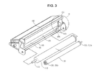
- FIG. 3 is an exploded perspective view of elements illustrated in FIG. 2
- FIG. 4 is an enlarged perspective view illustrating the portion 'B' of FIG. 3
- FIG. 5 is a sectional view taken along the line I-I of FIG. 2 in relation to a non-contact type developing method
- FIG. 6 is a sectional view taken along the line I-I of FIG. 2 in relation to a contact type developing method.
- a cleaning member 160 is provided in the housing 101.
- the cleaning member 160 serves to remove various foreign substances and the developer remaining on the surface of the photoconductor 113.
- the cleaning member 160 has an approximately rectangular blade shape and extends lengthwise in an axial direction of the rotating shaft 120a that supports the developer delivery member 120.
- the cleaning member 160 is coupled to the housing 101 via a bracket 190.
- the bracket 190 has a coupling portion 192 to secure the cleaning member 160 so as to assist in coupling the cleaning member 160 inside the housing 101.
- the cleaning member 160 is secured by the coupling portion 192 of the bracket 190, the cleaning member 160 is coupled to the housing 101 via the bracket 190 so as to come into contact with the outer peripheral surface of the photoconductor 113.
- the cleaning member 160 is formed of an elastic material, such as rubber, which allows the cleaning member 160 to always come into contact with the outer peripheral surface of the photoconductor 113 by elasticity thereof.
- a sealing member 170 is provided within the housing 101 and serves to prevent the developer removed by the cleaning member 160 from leaking from either side of the cleaning member 160.
- the sealing member 170 includes a fixing portion 172 fixed to the housing 101 and a contact portion 174 stepped from the fixing portion 172 so as to come into contact with either end of the cleaning member 160.
- the fixing portion 172 is provided with an adhesive member (not shown) such as a double-sided tape to fix the sealing member 170 to the housing 101.
- the sealing member 170 which is kept in contact with ends of the cleaning member 160, may act to absorb the developer once the developer has been removed from the surface of the photoconductor 113 and moved to either end of the cleaning member 160, or may act to move the developer to a waste developer storage chamber 104.
- An auxiliary sealing member 176 may also be coupled to one surface of the cleaning member 160.
- the auxiliary sealing member 176 is arranged to come into contact with the sealing member 170, so as to absorb the developer moved to either end of the cleaning member 160 or to move the developer to the waste developer storage chamber 104 in cooperation with the sealing member 170.
- the sealing member 170 and the auxiliary sealing member 176 may come into close contact with the photoconductor 113 by elasticity thereof and may be formed of a material suitable to absorb fine particles such as waste developer. For example, sponge or compressed felt to which Teflon has been added may be used.
- a film member 180 is provided below the cleaning member 160.
- the film member 180 is arranged to come into contact with the outer peripheral surface of the photoconductor 113 and serves to guide the developer and foreign substances removed by the cleaning member 160 into the waste developer storage chamber 104. Both ends of the film member 180 come into contact with the sealing member 170 to prevent the developer and foreign substances removed by the cleaning member 160 from leaking from the housing 101.
- the film member 180 may be a polyethyleneterephthalate (PET) film having elasticity.
- PET polyethyleneterephthalate
- the waste developer storage chamber 104 occupies a side region of the housing 101 and stores the developer removed from the surface of the photoconductor 113 by the cleaning member 160.
- the waste developer storage chamber 104 and the developing chamber 103 are partitioned from each other by the bracket 190, the cleaning member 160 is coupled to one end of the bracket 190, the sealing member 170 is in contact with the ends of the cleaning member 160, the film member 180 is provided at a lower end of the cleaning member 160 and the photoconductor 113, and the outer peripheral surface of the photoconductor 113 comes into contact with the cleaning member 160 and the film member 180. Accordingly, the waste developer storage chamber 104 prevents the developer and foreign substances introduced therein from leaking to the outside of the housing 101 or into the developing chamber 103.
- space maintaining members 130 may be rotatably installed on the rotating shaft 120a of the developer delivery member 120 such that an outer peripheral surface of each space maintaining member 130 comes into contact with the photoconductor 113.
- the space maintaining members 130 are engaged with the photoconductor 113 so as to be rotated during rotation of the photoconductor 113.
- space maintaining members 130a may be arranged at opposite ends of the rotating shaft 120a with the developer delivery member 120 interposed therebetween. In both the above cases, a distance between the space maintaining members 130 or 130a arranged respectively at opposite ends of the rotating shaft 120a is greater than a width of the paper, which prevents the paper from interfering with the space maintaining members 130 or 130a when the paper is delivered to the photoconductor 113.
- the space maintaining members 130 have an outer diameter greater than an outer diameter of the developer delivery member 120. As such, the space maintaining members 130 serve to maintain a constant developing gap G between the developer delivery member 120 and the photoconductor 113.
- the space maintaining members 130a have an outer diameter less than an outer diameter of the developer delivery member 120. As such, the space maintaining members 130a serve to maintain a constant developing nip N between the developer delivery member 120 and the photoconductor 113.
- the space maintaining members 130 or 130a to maintain a constant developing gap G or a constant developing nip N are arranged so as not to be contaminated by the developer or other foreign substances removed by the cleaning member 160.
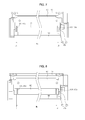
- FIG. 7 is a view illustrating a positional relationship between the cleaning member 160 and the space maintaining member 130 or 130a
- FIG. 8 is a view illustrating a positional relationship between the sealing member 170 and the space maintaining member 130 or 130a.
- illustration of the photoconductor and the developer delivery member is omitted.
- the space maintaining members 130 or 130a are inwardly spaced apart from both ends of the cleaning member 160 so as not to overlap with imaginary lines La and Lb extending from the respective ends of the cleaning member 160 in a direction perpendicular to a center rotation axis of the photoconductor 113.
- a width Wa between the imaginary lines La and Lb extending from both ends of the cleaning member 160 defines an area in which the cleaning member 160 comes into contact with the photoconductor 113 to enable removal of the developer and foreign substances from the surface of the photoconductor 113.
- the space maintaining members 130 or 130a which are located inside the imaginary lines La and Lb so as not to overlap with the imaginary lines La and Lb, are free from contamination by the developer or foreign substances.
- the photoconductor 113 receives the developer from the developer delivery member 120 while being rotated in a direction designated by the arrow and successively, transfers the developer to the paper delivered to the photoconductor 113.
- the developer which remains on the surface of the photoconductor 113 after transfer to the paper, is removed by the cleaning member 160, thereby being introduced into the waste developer storage chamber 104 or absorbed by the sealing member 170. Since the space maintaining members 130 always come into contact with the surface of the photoconductor 113 on which no developer or other foreign substances remain by operation of the cleaning member 160, it is possible to prevent the space maintaining members 130 from being contaminated by the developer or foreign substances.
- a distance between each space maintaining member 130 or 130a and the corresponding imaginary line La or Lb may be 20 mm or less. As described above, the distance between the pair of space maintaining members 130 or 130a must be greater than the width of the paper. Thus, if the distance between the space maintaining member 130 or 130a and the corresponding imaginary line La or Lb is excessively great, it may be difficult to achieve the greater distance between the pair of space maintaining members 130 or 130a than the width of the paper because this needs to excessively increase a width of the entire housing 101 containing the photoconductor 113 and the developer delivery member 120.
- each space maintaining member 130 or 130a may be inwardly spaced apart from one end of the contact portion 174 of the sealing member 170 so as not to overlap with an imaginary line Lc or Ld extending from the end of the contact portion 174 in a direction perpendicular to the center rotation axis of the photoconductor 113.
- the cleaning member 160 is adapted to scrape the developer and foreign substances remaining on the surface of the photoconductor 113 while coming into contact with the surface of the rotating photoconductor 113. Although most of the developer and foreign substances scraped by the cleaning member 160 are separated from the surface of the photoconductor 113 and introduced into the waste developer storage chamber 104, a part of the developer and foreign substances may move toward a rotating shaft 119 which rotatably supports the photoconductor 113 during rotation of the photoconductor 113, rather than being introduced into the waste developer storage chamber 104. The developer and foreign substances moved toward the rotating shaft 119 are collected at both ends of the cleaning member 160, thereby being absorbed by the sealing member 170 or being guided into the waste developer storage chamber 104.
- the sealing member 170 has a fixed volume although it is formed of a material suitable to absorb fine particles such as developer and thus, absorbs only a limited quantity of developer. If the sealing member 170 is saturated with the developer and foreign substances supplied thereto by the cleaning member 160, a part of the developer and foreign substances, not absorbed by the sealing member 170, remain on the surface of the photoconductor 113 in contact with the sealing member 170.
- the surface of the photoconductor 113 located in a width Wb between the imaginary line Lc and the imaginary line Ld is free from contamination by the developer and foreign substances not absorbed by the sealing member 170, or is repeatedly cleaned while continuously coming into contact with the cleaning member 160 even if it is partially contaminated.
- the space maintaining members 130 or 130a arranged between the imaginary lines Lc and Ld so as not to overlap with the imaginary lines Lc and Ld are free from contamination by the developer and foreign substances.
- the width Wb between the imaginary line Lc and the imaginary line Ld is equal to a width of an entrance 105 of the waste developer storage chamber 104. This is because the entrance 105 is defined by the cleaning member 160, the sealing members 170 in contact with both ends of the cleaning member 160 and the film member 180 provided at the lower end of the cleaning member 160 and thus, the width of the entrance 105 is equal to a distance between the contact portions 174 of the sealing members 170.
- the embodiment of the present inventive concept provides an image forming apparatus in which a developer delivery member is adapted to feed developer to a photoconductor at a predetermined position with respect to the photoconductor, which may prevent printing defects.
Landscapes
- Physics & Mathematics (AREA)
- General Physics & Mathematics (AREA)
- Engineering & Computer Science (AREA)
- Computer Vision & Pattern Recognition (AREA)
- Cleaning In Electrography (AREA)
- Dry Development In Electrophotography (AREA)
Abstract
Description
- Embodiments of the present inventive concept relate to an image forming apparatus in which a space maintaining member to maintain a constant developing nip or developing gap between a photoconductor and a developer delivery member has an improved position.
- An image forming apparatus is designed to form an image on a print medium according to input signals. Examples of image forming apparatuses include printers, copiers, fax machines, and devices combining functions thereof.
- In an electro-photographic image forming apparatus, a photoconductor, which has been charged with a predetermined electric potential, is exposed to light such that an electrostatic latent image is formed on a surface of the photoconductor. Developer is fed to the electrostatic latent image to form a visible image and thereafter, the visible image is transferred and fused to paper, completing printing of the image on the paper.
- In general, methods of arranging a developer delivery member include a contact type method in which the developer delivery member comes into contact with the photoconductor to feed developer to the photoconductor, and a non-contact type method in which the developer delivery member is spaced apart from the photoconductor by a constant distance to feed developer to the photoconductor.
- In the case of the contact type method, a developing nip is defined between the photoconductor and the developer delivery member, and in the case of the non-contact type method, a developing gap is defined between the photoconductor and the developer delivery member. Both the contact type method and the non-contact type method adopt a contact member, which comes into contact with the photoconductor to maintain a constant developing nip or developing gap.
- A space maintaining member is located on the same axis as the developer delivery member so as to rotate together with the developer delivery member. As the space maintaining member is rotated in contact with an outer peripheral surface of the photoconductor, a constant developing nip or developing gap between the photoconductor and the developer delivery member is maintained. However, if foreign substances accumulate and attach to the space maintaining member, the radius of the space maintaining member locally increases due to buildup of the substances, which makes it difficult to maintain a constant developing nip or developing gap between the photoconductor and the developer delivery member and results in periodic image printing defects.
- The present inventive concept provides an image forming apparatus having an improved configuration to prevent foreign substances from accumulating on a space maintaining member that is used to maintain a constant developing nip or developing gap between a photoconductor and a developer delivery member.
- Additional features and utilities of the present inventive concept will be set forth in part in the description which follows and, in part, will be obvious from the description, or may be learned by practice of the invention.
- According to the present invention there is provided an apparatus and method as set forth in the appended claims. Other features of the invention will be apparent from the dependent claims, and the description which follows.
- In accordance with an exemplary embodiment, a developing device includes a photoconductor, a developer delivery member to deliver and feed developer to the photoconductor, a cleaning member to remove developer and foreign substances remaining on a surface of the photoconductor while coming into contact with the photoconductor, and space maintaining members arranged to directly or indirectly come into contact with the photoconductor so as to maintain a constant developing gap or developing nip between the photoconductor and the developer delivery member, wherein the space maintaining members are located between both ends of the cleaning member.
- The developing device may further include sealing members respectively located at both ends of the cleaning member to prevent leakage of the developer, and the space maintaining members may be located between the sealing members.
- Each of the sealing members may include a contact portion to come into contact with both ends of the photoconductor, and the space maintaining members may be located between the contact portions of the sealing members.
- The developing device may further include auxiliary sealing members coupled to a surface of the cleaning member and arranged to come into contact with the respective sealing members so as to prevent leakage of the developer in cooperation with the sealing members.
- The space maintaining members may be located between the auxiliary sealing members.
- The space maintaining members may be provided at the outer side of both ends of the developer delivery member, and a distance between the space maintaining members may be greater than a width of paper delivered to the photoconductor.
- Each of the space maintaining members may be spaced apart from one end of the cleaning member by a distance of about 20 mm or less.
- In accordance with another exemplary embodiment, an image forming apparatus includes a main body, a housing mounted in the main body, a photoconductor rotatably coupled to the housing, a developer delivery member arranged near the photoconductor to deliver developer to the photoconductor, a cleaning blade arranged to come into contact with a surface of the photoconductor so as to remove the developer remaining on the surface of the photoconductor, sealing members arranged to come into contact with both ends of the cleaning blade so as to prevent leakage of the developer, and a space maintaining member arranged within an area to be cleaned by the cleaning blade and serving to maintain a constant developing gap or developing nip between the photoconductor and the developer delivery member.
- The image forming apparatus may further include a waste developer storage chamber in which the developer removed from the surface of the photoconductor is stored, and a film member arranged below the cleaning blade to define an entrance of the waste developer storage chamber along with the cleaning blade and the sealing members.
- The space maintaining member may be located inside both ends of the entrance.
- Each of the sealing members may include a fixing portion fixed to one side of the housing and a contact portion to come into contact with the cleaning blade, and the space maintaining member may be located between the contact portions of the sealing members.
- In accordance with another exemplary embodiment, a developing device usable with an image forming apparatus includes: a photoconductor to receive developer; a cleaning member extending along a length of the photoconductor and to remove remaining developer from the photoconductor; and a developer delivery member to deliver the developer to the photoconductor, the developer delivery member including space maintaining members disposed at each end thereof to contact respective ends of the photoconductor to maintain a space or nip between the developer delivery member and the photoconductor, the space maintaining members being disposed at positions inside a region defined by ends of the cleaning member
- In an embodiment, the developing device further includes sealing members disposed at each end of the cleaning member to contact respective ends of the photoconductor to absorb developer remaining at ends of the cleaning member and to prevent leakage of the developer past the ends of the cleaning member.
- In an embodiment, the space maintaining members are disposed inside a region defined by the sealing members.
- In an embodiment, the sealing members overlap a portion of the ends of the cleaning members.
- In an embodiment, the developing device further includes a waste developer storage chamber in which the developer removed from the surface of the photoconductor is stored; and a film member disposed below the cleaning blade to define an entrance of the waste developer storage chamber along with the cleaning blade and the sealing members.
- In accordance with another exemplary embodiment, an image forming apparatus includes a developer housing mounted therein, the housing comprising: a photoconductor disposed therein to receive developer; a developer delivery member to deliver developer to the photoconductor; a cleaning member disposed to contact a surface of the photoconductor to clean the surface of the photoconductor of remaining developer; and a space maintaining member disposed between the developer deliver member and the photoconductor to maintain a constant developing gap or developing nip therebetween and provided within a region in which the cleaning member cleans the surface of the photoconductor.
- In an embodiment, the image forming apparatus further includes sealing members disposed within the housing at respective ends of the cleaning member to absorb developer extending past the ends of the cleaning member.
- In an embodiment, the space maintaining member is disposed within a region between the sealing members.
- In an embodiment, the space maintaining member comprises first and second space maintaining members disposed at opposite ends of the developer deliver member.
- These and/or other features of the inventive concept will become apparent and more readily appreciated from the following description of the embodiments, taken in conjunction with the accompanying drawings of which:
-
FIG. 1 is a view schematically illustrating a configuration of an image forming apparatus according to an embodiment of the present inventive concept; -
FIG. 2 is an enlarged perspective view illustrating main elements of the portion 'A' ofFIG. 1 ; -
FIG. 3 is an exploded perspective view of elements illustrated inFIG. 2 ; -
FIG. 4 is an enlarged perspective view illustrating the portion 'B' ofFIG. 3 ; -
FIG. 5 is a sectional view taken along the line I-I ofFIG. 2 in relation to a non-contact type developing method; -
FIG. 6 is a sectional view taken along the line I-I ofFIG. 2 in relation to a contact type developing method; -
FIG. 7 is a view illustrating a positional relationship between a cleaning member and a space maintaining member; and -
FIG. 8 is a view illustrating a positional relationship between a sealing member and a space maintaining member. - Reference will now be made in detail to the embodiments of the present general inventive concept, examples of which are illustrated in the accompanying drawings, wherein like reference numerals refer to the like elements throughout. The embodiments are described below in order to explain the present general inventive concept while referring to the figures.
-
FIG. 1 is a view schematically illustrating a configuration of an image forming apparatus according to an embodiment of the present inventive concept. - As illustrated in
FIG. 1 , the image forming apparatus includes amain body 10, which defines an external appearance of the image forming apparatus and supports a variety of constituent elements installed in the image forming apparatus, apaper feeding device 20 to feed printing media, i.e. paper S, a developingdevice 100 to develop an image on the paper, afusing device 30 to fuse the developed image on the paper by applying heat and pressure to the paper, and apaper discharge device 40 to discharge the paper, on which the image has been completely printed, to the outside of themain body 10. - The
paper feeding device 20 includes apaper feeding cassette 21 in which the paper S is stored, a pickup roller 22 to pick up the paper S stored in thepaper feeding cassette 21 sheet by sheet, and adelivery roller 23 to move the picked-up paper toward the developingdevice 100. - The developing
device 100 includes ahousing 101, which defines an external appearance of the developingdevice 100 and supports a variety of constituent elements installed in the developingdevice 100. Thehousing 101 contains adeveloper storage chamber 102 in which developer is stored, and a developingchamber 103 in which a developing operation is performed using the developer fed from thedeveloper storage chamber 102. - The
developer storage chamber 102 is provided with anagitating blade 111 and afeed roller 112. The agitatingblade 111 serves to agitate the developer stored in thedeveloper storage chamber 102, thereby preventing the developer from hardening. Thefeed roller 112 serves to feed the developer from thedeveloper storage chamber 102 to the developingchamber 103. Thefeed roller 112 is rotated in contact with adeveloper delivery member 120 which will be described hereinafter, thereby feeding the developer to thedeveloper delivery member 120. - The developing
chamber 103 is provided with aphotoconductor 113, on a surface of which an electrostatic latent image is formed by anexposure device 50 based on image information. The developingchamber 102 is further provided with a charging roller 114 to charge the surface of thephotoconductor 113 with a predetermined electric potential. Thedeveloper delivery member 120 is installed in the developingchamber 103 and serves to deliver the developer fed by thefeed roller 112 to thephotoconductor 113 so as to develop the electrostatic latent image formed on thephotoconductor 113 to a visible image. Thedeveloper delivery member 120 is rotatably supported at opposite lateral surfaces of thehousing 101 using a rotating shaft (120a, seeFIG. 2 ). - A regulating
member 115 is installed in thehousing 101. The regulatingmember 115 serves to regulate the thickness of a developer layer when the developer is adhered to a surface of thedeveloper delivery member 120 by thefeed roller 112. -
FIG. 2 is an enlarged perspective view illustrating main elements of the portion 'A' ofFIG. 1 ,FIG. 3 is an exploded perspective view of elements illustrated inFIG. 2 ,FIG. 4 is an enlarged perspective view illustrating the portion 'B' ofFIG. 3 ,FIG. 5 is a sectional view taken along the line I-I ofFIG. 2 in relation to a non-contact type developing method, andFIG. 6 is a sectional view taken along the line I-I ofFIG. 2 in relation to a contact type developing method. - As illustrated in
FIGS. 2 to 6 , a cleaningmember 160 is provided in thehousing 101. The cleaningmember 160 serves to remove various foreign substances and the developer remaining on the surface of thephotoconductor 113. The cleaningmember 160 has an approximately rectangular blade shape and extends lengthwise in an axial direction of therotating shaft 120a that supports thedeveloper delivery member 120. - The cleaning
member 160 is coupled to thehousing 101 via abracket 190. Thebracket 190 has acoupling portion 192 to secure the cleaningmember 160 so as to assist in coupling the cleaningmember 160 inside thehousing 101. As the cleaningmember 160 is secured by thecoupling portion 192 of thebracket 190, the cleaningmember 160 is coupled to thehousing 101 via thebracket 190 so as to come into contact with the outer peripheral surface of thephotoconductor 113. - The cleaning
member 160 is formed of an elastic material, such as rubber, which allows the cleaningmember 160 to always come into contact with the outer peripheral surface of thephotoconductor 113 by elasticity thereof. - A sealing
member 170 is provided within thehousing 101 and serves to prevent the developer removed by the cleaningmember 160 from leaking from either side of the cleaningmember 160. The sealingmember 170 includes a fixingportion 172 fixed to thehousing 101 and acontact portion 174 stepped from the fixingportion 172 so as to come into contact with either end of the cleaningmember 160. The fixingportion 172 is provided with an adhesive member (not shown) such as a double-sided tape to fix the sealingmember 170 to thehousing 101. The sealingmember 170, which is kept in contact with ends of the cleaningmember 160, may act to absorb the developer once the developer has been removed from the surface of thephotoconductor 113 and moved to either end of the cleaningmember 160, or may act to move the developer to a wastedeveloper storage chamber 104. - An
auxiliary sealing member 176 may also be coupled to one surface of the cleaningmember 160. Theauxiliary sealing member 176 is arranged to come into contact with the sealingmember 170, so as to absorb the developer moved to either end of the cleaningmember 160 or to move the developer to the wastedeveloper storage chamber 104 in cooperation with the sealingmember 170. - The sealing
member 170 and theauxiliary sealing member 176 may come into close contact with thephotoconductor 113 by elasticity thereof and may be formed of a material suitable to absorb fine particles such as waste developer. For example, sponge or compressed felt to which Teflon has been added may be used. - A
film member 180 is provided below the cleaningmember 160. Thefilm member 180 is arranged to come into contact with the outer peripheral surface of thephotoconductor 113 and serves to guide the developer and foreign substances removed by the cleaningmember 160 into the wastedeveloper storage chamber 104. Both ends of thefilm member 180 come into contact with the sealingmember 170 to prevent the developer and foreign substances removed by the cleaningmember 160 from leaking from thehousing 101. - The
film member 180 may be a polyethyleneterephthalate (PET) film having elasticity. - The waste
developer storage chamber 104 occupies a side region of thehousing 101 and stores the developer removed from the surface of thephotoconductor 113 by the cleaningmember 160. The wastedeveloper storage chamber 104 and the developingchamber 103 are partitioned from each other by thebracket 190, the cleaningmember 160 is coupled to one end of thebracket 190, the sealingmember 170 is in contact with the ends of the cleaningmember 160, thefilm member 180 is provided at a lower end of the cleaningmember 160 and thephotoconductor 113, and the outer peripheral surface of thephotoconductor 113 comes into contact with the cleaningmember 160 and thefilm member 180. Accordingly, the wastedeveloper storage chamber 104 prevents the developer and foreign substances introduced therein from leaking to the outside of thehousing 101 or into the developingchamber 103. - In some embodiments,
space maintaining members 130 may be rotatably installed on therotating shaft 120a of thedeveloper delivery member 120 such that an outer peripheral surface of eachspace maintaining member 130 comes into contact with thephotoconductor 113. Thespace maintaining members 130 are engaged with thephotoconductor 113 so as to be rotated during rotation of thephotoconductor 113. In some embodiments,space maintaining members 130a may be arranged at opposite ends of therotating shaft 120a with thedeveloper delivery member 120 interposed therebetween. In both the above cases, a distance between thespace maintaining members rotating shaft 120a is greater than a width of the paper, which prevents the paper from interfering with thespace maintaining members photoconductor 113. - As illustrated in
FIG. 5 , in the case of a non-contact type developing method in which thedeveloper delivery member 120 does not come into contact with thephotoconductor 113 and defines a developing gap G with thephotoconductor 113 to feed developer, thespace maintaining members 130 have an outer diameter greater than an outer diameter of thedeveloper delivery member 120. As such, thespace maintaining members 130 serve to maintain a constant developing gap G between thedeveloper delivery member 120 and thephotoconductor 113. - As illustrated in
FIG. 6 , in the case of a contact type developing method in which thedeveloper delivery member 120 comes into contact with thephotoconductor 113 to define a developing nip N with thephotoconductor 113 to feed developer, thespace maintaining members 130a have an outer diameter less than an outer diameter of thedeveloper delivery member 120. As such, thespace maintaining members 130a serve to maintain a constant developing nip N between thedeveloper delivery member 120 and thephotoconductor 113. - The
space maintaining members member 160. -
FIG. 7 is a view illustrating a positional relationship between the cleaningmember 160 and thespace maintaining member FIG. 8 is a view illustrating a positional relationship between the sealingmember 170 and thespace maintaining member FIGS. 7 and 8 , illustration of the photoconductor and the developer delivery member is omitted. - As illustrated in
FIG. 7 , thespace maintaining members member 160 so as not to overlap with imaginary lines La and Lb extending from the respective ends of the cleaningmember 160 in a direction perpendicular to a center rotation axis of thephotoconductor 113. - A width Wa between the imaginary lines La and Lb extending from both ends of the cleaning
member 160 defines an area in which the cleaningmember 160 comes into contact with thephotoconductor 113 to enable removal of the developer and foreign substances from the surface of thephotoconductor 113. As the surface of thephotoconductor 113 located in the width Wa between the imaginary lines La and Lb is repeatedly cleaned while continuously coming into contact with the cleaningmember 160, thespace maintaining members - Explaining the above described configuration in more detail with reference to
FIG. 5 , thephotoconductor 113 receives the developer from thedeveloper delivery member 120 while being rotated in a direction designated by the arrow and successively, transfers the developer to the paper delivered to thephotoconductor 113. The developer, which remains on the surface of thephotoconductor 113 after transfer to the paper, is removed by the cleaningmember 160, thereby being introduced into the wastedeveloper storage chamber 104 or absorbed by the sealingmember 170. Since thespace maintaining members 130 always come into contact with the surface of thephotoconductor 113 on which no developer or other foreign substances remain by operation of the cleaningmember 160, it is possible to prevent thespace maintaining members 130 from being contaminated by the developer or foreign substances. - Accordingly, as a result of arranging the
space maintaining members member 160 so as not to overlap with the imaginary lines La and Lb, it is possible to prevent the developer or foreign substances from accumulating on the surface of thespace maintaining members space maintaining members space maintaining members photoconductor 113. Consequently, it is possible to prevent a distance between the photoconductor 113 and thedeveloper delivery member 120 from becoming irregular due to developer or foreign substances becoming present on thespace maintaining members - A distance between each
space maintaining member space maintaining members space maintaining member space maintaining members entire housing 101 containing thephotoconductor 113 and thedeveloper delivery member 120. - As illustrated in
FIG. 8 , eachspace maintaining member contact portion 174 of the sealingmember 170 so as not to overlap with an imaginary line Lc or Ld extending from the end of thecontact portion 174 in a direction perpendicular to the center rotation axis of thephotoconductor 113. - The cleaning
member 160 is adapted to scrape the developer and foreign substances remaining on the surface of thephotoconductor 113 while coming into contact with the surface of therotating photoconductor 113. Although most of the developer and foreign substances scraped by the cleaningmember 160 are separated from the surface of thephotoconductor 113 and introduced into the wastedeveloper storage chamber 104, a part of the developer and foreign substances may move toward arotating shaft 119 which rotatably supports thephotoconductor 113 during rotation of thephotoconductor 113, rather than being introduced into the wastedeveloper storage chamber 104. The developer and foreign substances moved toward therotating shaft 119 are collected at both ends of the cleaningmember 160, thereby being absorbed by the sealingmember 170 or being guided into the wastedeveloper storage chamber 104. - The sealing
member 170 has a fixed volume although it is formed of a material suitable to absorb fine particles such as developer and thus, absorbs only a limited quantity of developer. If the sealingmember 170 is saturated with the developer and foreign substances supplied thereto by the cleaningmember 160, a part of the developer and foreign substances, not absorbed by the sealingmember 170, remain on the surface of thephotoconductor 113 in contact with the sealingmember 170. - The surface of the
photoconductor 113 located in a width Wb between the imaginary line Lc and the imaginary line Ld is free from contamination by the developer and foreign substances not absorbed by the sealingmember 170, or is repeatedly cleaned while continuously coming into contact with the cleaningmember 160 even if it is partially contaminated. Thus, thespace maintaining members - The width Wb between the imaginary line Lc and the imaginary line Ld is equal to a width of an
entrance 105 of the wastedeveloper storage chamber 104. This is because theentrance 105 is defined by the cleaningmember 160, the sealingmembers 170 in contact with both ends of the cleaningmember 160 and thefilm member 180 provided at the lower end of the cleaningmember 160 and thus, the width of theentrance 105 is equal to a distance between thecontact portions 174 of the sealingmembers 170. - As is apparent from the above description, the embodiment of the present inventive concept provides an image forming apparatus in which a developer delivery member is adapted to feed developer to a photoconductor at a predetermined position with respect to the photoconductor, which may prevent printing defects.
- Although a few embodiments of the present general inventive concept have been shown and described, it will be appreciated by those skilled in the art that changes may be made in these embodiments without departing from the principles of the general inventive concept, the scope of which is defined in the appended claims and their equivalents.
- Attention is directed to all papers and documents which are filed concurrently with or previous to this specification in connection with this application and which are open to public inspection with this specification, and the contents of all such papers and documents are incorporated herein by reference.
- All of the features disclosed in this specification (including any accompanying claims, abstract and drawings), and/or all of the steps of any method or process so disclosed, may be combined in any combination, except combinations where at least some of such features and/or steps are mutually exclusive.
- Each feature disclosed in this specification (including any accompanying claims, abstract and drawings) may be replaced by alternative features serving the same, equivalent or similar purpose, unless expressly stated otherwise. Thus, unless expressly stated otherwise, each feature disclosed is one example only of a generic series of equivalent or similar features.
- The invention is not restricted to the details of the foregoing embodiment(s). The invention extends to any novel one, or any novel combination, of the features disclosed in this specification (including any accompanying claims, abstract and drawings), or to any novel one, or any novel combination, of the steps of any method or process so disclosed.
Claims (21)
- A developing device comprising:a photoconductor;a developer delivery member to deliver and feed developer to the photoconductor;a cleaning member to remove developer and foreign substances remaining on a surface of the photoconductor while coming into contact with the photoconductor; andspace maintaining members arranged to directly or indirectly come into contact with the photoconductor so as to maintain a constant developing gap or developing nip between the photoconductor and the developer delivery member, the space maintaining members being located between both ends of the cleaning member.
- The developing device according to claim 1, further comprising:sealing members respectively located at both ends of the cleaning member to prevent leakage of the developer,wherein the space maintaining members are located between the sealing members.
- The developing device according to claim 2, wherein:each of the sealing members includes a contact portion to come into contact with respective ends of the photoconductor; andthe space maintaining members are located between the contact portions of the sealing members.
- The developing device according to claim 3, further comprising:auxiliary sealing members coupled to a surface of the cleaning member and arranged to come into contact with the respective sealing members so as to prevent leakage of the developer in cooperation with the sealing members.
- The developing device according to claim 4, wherein the space maintaining members are located between the auxiliary sealing members.
- The developing device according to claim 1, wherein:the space maintaining members are provided at the outer side of both ends of the developer delivery member; anda distance between the space maintaining members is greater than a width of paper delivered to the photoconductor.
- The developing device according to claim 1, wherein each of the space maintaining members is spaced apart from one end of the cleaning member by a distance of about 20 mm or less.
- An image forming apparatus comprising:a main body;a housing mounted in the main body;a photoconductor rotatably coupled to the housing;a developer delivery member arranged near the photoconductor to deliver developer to the photoconductor;a cleaning blade arranged to come into contact with a surface of the photoconductor to remove the developer remaining on the surface of the photoconductor;sealing members arranged to come into contact with both ends of the cleaning blade to prevent leakage of the developer; anda space maintaining member arranged within an area to be cleaned by the cleaning blade and serving to maintain a constant developing gap or developing nip between the photoconductor and the developer delivery member.
- The image forming apparatus according to claim 8, further comprising:a waste developer storage chamber in which the developer removed from the surface of the photoconductor is stored; anda film member arranged below the cleaning blade to define an entrance of the waste developer storage chamber along with the cleaning blade and the sealing members.
- The image forming apparatus according to claim 9, wherein the space maintaining member is located inside both ends of the entrance.
- The image forming apparatus according to claim 10, wherein:each of the sealing members includes a fixing portion fixed to one side of the housing and a contact portion to come into contact with the cleaning blade; andthe space maintaining member is located between the contact portions of the sealing members.
- A developing device usable with an image forming apparatus, the developing device comprising:a photoconductor to receive developer;a cleaning member extending along a length of the photoconductor and to remove remaining developer from the photoconductor; anda developer delivery member to deliver the developer to the photoconductor, the developer delivery member including space maintaining members disposed at each end thereof to contact respective ends of the photoconductor to maintain a space or nip between the developer delivery member and the photoconductor, the space maintaining members being disposed at positions inside a region defined by ends of the cleaning member.
- The developing device of claim 12, further comprising:sealing members disposed at each end of the cleaning member to contact respective ends of the photoconductor to absorb developer remaining at ends of the cleaning member and to prevent leakage of the developer past the ends of the cleaning member.
- The developing device of claim 13, wherein the space maintaining members are disposed inside a region defined by the sealing members.
- The developing device of claim 14, wherein the sealing members overlap a portion of the ends of the cleaning members.
- The developing device of claim 13, further comprising:a waste developer storage chamber in which the developer removed from the surface of the photoconductor is stored; anda film member disposed below the cleaning blade to define an entrance of the waste developer storage chamber along with the cleaning blade and the sealing members.
- An image forming apparatus comprising:a developer housing mounted therein, the housing comprising;a photoconductor disposed therein to receive developer;a developer delivery member to deliver developer to the photoconductor;a cleaning member disposed to contact a surface of the photoconductor to clean the surface of the photoconductor of remaining developer; anda space maintaining member disposed between the developer deliver member and the photoconductor to maintain a constant developing gap or developing nip therebetween and provided within a region in which the cleaning member cleans the surface of the photoconductor.
- The image forming apparatus of claim 17, further comprising:sealing members disposed within the housing at respective ends of the cleaning member to absorb developer extending past the ends of the cleaning member.
- The image forming apparatus of claim 18, wherein the space maintaining member is disposed within a region between the sealing members.
- The image forming apparatus of claim 19, wherein the space maintaining member comprises first and second space maintaining members disposed at opposite ends of the developer deliver member.
- The image forming apparatus of claim 18, wherein the developer housing further comprises:a waste developer storage chamber in which the developer removed from the surface of the photoconductor is stored; anda film member disposed below the cleaning blade to define an entrance of the waste developer storage chamber along with the cleaning blade and the sealing members.
Applications Claiming Priority (2)
| Application Number | Priority Date | Filing Date | Title |
|---|---|---|---|
| KR20100135438 | 2010-12-27 | ||
| KR1020110125224A KR20120074204A (en) | 2010-12-27 | 2011-11-28 | Developing device of image forming apparatus |
Publications (2)
| Publication Number | Publication Date |
|---|---|
| EP2469344A1 true EP2469344A1 (en) | 2012-06-27 |
| EP2469344B1 EP2469344B1 (en) | 2018-04-11 |
Family
ID=45464302
Family Applications (1)
| Application Number | Title | Priority Date | Filing Date |
|---|---|---|---|
| EP11195194.3A Not-in-force EP2469344B1 (en) | 2010-12-27 | 2011-12-22 | Developing device of image forming apparatus |
Country Status (2)
| Country | Link |
|---|---|
| US (1) | US8837986B2 (en) |
| EP (1) | EP2469344B1 (en) |
Families Citing this family (10)
| Publication number | Priority date | Publication date | Assignee | Title |
|---|---|---|---|---|
| JP5645892B2 (en) * | 2012-08-01 | 2014-12-24 | キヤノン株式会社 | Cleaning device, cartridge, image forming apparatus, and elastic seal |
| JP6161245B2 (en) * | 2012-09-13 | 2017-07-12 | キヤノン株式会社 | Cleaning unit, process cartridge, image forming apparatus |
| US9146526B2 (en) | 2012-09-13 | 2015-09-29 | Canon Kabushiki Kaisha | Unit, cleaning unit, process cartridge, and image forming apparatus |
| JP6198524B2 (en) * | 2012-09-27 | 2017-09-20 | キヤノン株式会社 | Cleaning unit, process cartridge including cleaning unit, and image forming apparatus including cleaning unit |
| JP2014071428A (en) * | 2012-10-01 | 2014-04-21 | Canon Inc | Process cartridge |
| JP6274892B2 (en) * | 2014-02-04 | 2018-02-07 | キヤノン株式会社 | Developer container, cartridge, image forming apparatus |
| JP6287336B2 (en) * | 2014-02-28 | 2018-03-07 | ブラザー工業株式会社 | Process cartridge and photoreceptor unit |
| JP6456152B2 (en) * | 2015-01-15 | 2019-01-23 | キヤノン株式会社 | Cleaning device |
| US9891578B2 (en) * | 2015-12-29 | 2018-02-13 | Lexmark International, Inc. | Cleaner blade sealing in an electrophotographic image forming device |
| CN109778622B (en) * | 2017-11-13 | 2022-02-25 | 宝马汽车股份有限公司 | Work system and transportation system |
Citations (2)
| Publication number | Priority date | Publication date | Assignee | Title |
|---|---|---|---|---|
| JPH11119548A (en) * | 1997-10-09 | 1999-04-30 | Canon Inc | Image forming device |
| US20090269106A1 (en) * | 2008-04-24 | 2009-10-29 | Kyocera Mita Corporation | Image forming apparatus |
Family Cites Families (8)
| Publication number | Priority date | Publication date | Assignee | Title |
|---|---|---|---|---|
| US4331754A (en) * | 1975-10-02 | 1982-05-25 | Xerox Corporation | Self-spacing touchdown development method |
| US5293199A (en) * | 1990-05-11 | 1994-03-08 | Minolta Camera Kabushiki Kaisha | Image forming apparatus having spacing roller for maintaining uniform spacing between image bearing member and developing material supplying means |
| TW290661B (en) * | 1993-08-30 | 1996-11-11 | Canon Kk | |
| JP2004144803A (en) * | 2002-10-22 | 2004-05-20 | Canon Inc | Developing device and process cartridge |
| CN100520620C (en) * | 2002-11-20 | 2009-07-29 | 精工爱普生株式会社 | Developer roller, developing unit, image formation device and computer system |
| KR20080073477A (en) * | 2007-02-06 | 2008-08-11 | 삼성전자주식회사 | Image forming apparatus and developing device |
| JP5151774B2 (en) * | 2008-07-29 | 2013-02-27 | 株式会社リコー | Cleaning device, process unit, and image forming apparatus |
| JP2011253173A (en) * | 2010-05-07 | 2011-12-15 | Ricoh Co Ltd | Process unit and image forming apparatus |
-
2011
- 2011-12-22 EP EP11195194.3A patent/EP2469344B1/en not_active Not-in-force
- 2011-12-27 US US13/337,641 patent/US8837986B2/en active Active
Patent Citations (2)
| Publication number | Priority date | Publication date | Assignee | Title |
|---|---|---|---|---|
| JPH11119548A (en) * | 1997-10-09 | 1999-04-30 | Canon Inc | Image forming device |
| US20090269106A1 (en) * | 2008-04-24 | 2009-10-29 | Kyocera Mita Corporation | Image forming apparatus |
Also Published As
| Publication number | Publication date |
|---|---|
| US20120163855A1 (en) | 2012-06-28 |
| EP2469344B1 (en) | 2018-04-11 |
| US8837986B2 (en) | 2014-09-16 |
Similar Documents
| Publication | Publication Date | Title |
|---|---|---|
| US8837986B2 (en) | Developing device of image forming apparatus | |
| US7962060B2 (en) | Cleaning and sealing apparatus of an image forming apparatus and developing unit thereof | |
| EP1865387A1 (en) | Charging roller cleaning device and image forming apparatus including the same | |
| CN107643664B (en) | Image forming apparatus, process cartridge, and developing cartridge | |
| US20110097123A1 (en) | Cleaning device for photosensitive drum and image forming apparatus equipped with cleaning device | |
| US9335705B1 (en) | Rotor bearing member, photoconductor unit including the same, and image forming apparatus | |
| JP7567438B2 (en) | Toner conveying device, cleaning device, image forming device | |
| JP2004086234A (en) | Cleaning device | |
| JP5717285B2 (en) | Cleaning device and image forming apparatus equipped with the same | |
| JP5216745B2 (en) | Image forming apparatus | |
| CN102385298B (en) | Cleaning device, image processing system and clean method | |
| JP5806975B2 (en) | Image forming apparatus | |
| JP4674493B2 (en) | Image forming apparatus | |
| US7386260B2 (en) | Liquid developing unit and image forming apparatus including the same | |
| JP3669220B2 (en) | Image forming apparatus and manufacturing method thereof | |
| JP2000206850A (en) | Paper dust removal equipment for image forming equipment | |
| JP2000235336A (en) | Image forming device and cleaning device | |
| JP3631673B2 (en) | Image forming apparatus | |
| JP5634276B2 (en) | Cleaning device and image forming apparatus equipped with the same | |
| JP2010256829A (en) | Drum unit and image forming apparatus incorporating the same | |
| JP2012098502A (en) | Image forming apparatus | |
| KR100667786B1 (en) | Developing apparatus of image forming apparatus | |
| JP2014112152A (en) | Image forming apparatus | |
| JP2011095356A (en) | Cleaning device and image forming apparatus having the same | |
| JP2013242375A (en) | Cleaning device, and image carrier unit including the same, and image forming apparatus |
Legal Events
| Date | Code | Title | Description |
|---|---|---|---|
| AK | Designated contracting states |
Kind code of ref document: A1 Designated state(s): AL AT BE BG CH CY CZ DE DK EE ES FI FR GB GR HR HU IE IS IT LI LT LU LV MC MK MT NL NO PL PT RO RS SE SI SK SM TR |
|
| AX | Request for extension of the european patent |
Extension state: BA ME |
|
| PUAI | Public reference made under article 153(3) epc to a published international application that has entered the european phase |
Free format text: ORIGINAL CODE: 0009012 |
|
| RAP1 | Party data changed (applicant data changed or rights of an application transferred) |
Owner name: SAMSUNG ELECTRONICS CO., LTD. |
|
| 17P | Request for examination filed |
Effective date: 20121227 |
|
| 17Q | First examination report despatched |
Effective date: 20160818 |
|
| STAA | Information on the status of an ep patent application or granted ep patent |
Free format text: STATUS: EXAMINATION IS IN PROGRESS |
|
| RAP1 | Party data changed (applicant data changed or rights of an application transferred) |
Owner name: S-PRINTING SOLUTION CO., LTD. |
|
| GRAP | Despatch of communication of intention to grant a patent |
Free format text: ORIGINAL CODE: EPIDOSNIGR1 |
|
| STAA | Information on the status of an ep patent application or granted ep patent |
Free format text: STATUS: GRANT OF PATENT IS INTENDED |
|
| INTG | Intention to grant announced |
Effective date: 20171102 |
|
| GRAS | Grant fee paid |
Free format text: ORIGINAL CODE: EPIDOSNIGR3 |
|
| GRAA | (expected) grant |
Free format text: ORIGINAL CODE: 0009210 |
|
| STAA | Information on the status of an ep patent application or granted ep patent |
Free format text: STATUS: THE PATENT HAS BEEN GRANTED |
|
| AK | Designated contracting states |
Kind code of ref document: B1 Designated state(s): AL AT BE BG CH CY CZ DE DK EE ES FI FR GB GR HR HU IE IS IT LI LT LU LV MC MK MT NL NO PL PT RO RS SE SI SK SM TR |
|
| REG | Reference to a national code |
Ref country code: GB Ref legal event code: FG4D |
|
| REG | Reference to a national code |
Ref country code: CH Ref legal event code: EP |
|
| REG | Reference to a national code |
Ref country code: AT Ref legal event code: REF Ref document number: 988677 Country of ref document: AT Kind code of ref document: T Effective date: 20180415 |
|
| REG | Reference to a national code |
Ref country code: IE Ref legal event code: FG4D |
|
| REG | Reference to a national code |
Ref country code: DE Ref legal event code: R096 Ref document number: 602011047347 Country of ref document: DE |
|
| RAP2 | Party data changed (patent owner data changed or rights of a patent transferred) |
Owner name: HP PRINTING KOREA CO., LTD. |
|
| REG | Reference to a national code |
Ref country code: NL Ref legal event code: MP Effective date: 20180411 |
|
| REG | Reference to a national code |
Ref country code: LT Ref legal event code: MG4D |
|
| PG25 | Lapsed in a contracting state [announced via postgrant information from national office to epo] |
Ref country code: NL Free format text: LAPSE BECAUSE OF FAILURE TO SUBMIT A TRANSLATION OF THE DESCRIPTION OR TO PAY THE FEE WITHIN THE PRESCRIBED TIME-LIMIT Effective date: 20180411 |
|
| PG25 | Lapsed in a contracting state [announced via postgrant information from national office to epo] |
Ref country code: SE Free format text: LAPSE BECAUSE OF FAILURE TO SUBMIT A TRANSLATION OF THE DESCRIPTION OR TO PAY THE FEE WITHIN THE PRESCRIBED TIME-LIMIT Effective date: 20180411 Ref country code: AL Free format text: LAPSE BECAUSE OF FAILURE TO SUBMIT A TRANSLATION OF THE DESCRIPTION OR TO PAY THE FEE WITHIN THE PRESCRIBED TIME-LIMIT Effective date: 20180411 Ref country code: ES Free format text: LAPSE BECAUSE OF FAILURE TO SUBMIT A TRANSLATION OF THE DESCRIPTION OR TO PAY THE FEE WITHIN THE PRESCRIBED TIME-LIMIT Effective date: 20180411 Ref country code: PL Free format text: LAPSE BECAUSE OF FAILURE TO SUBMIT A TRANSLATION OF THE DESCRIPTION OR TO PAY THE FEE WITHIN THE PRESCRIBED TIME-LIMIT Effective date: 20180411 Ref country code: LT Free format text: LAPSE BECAUSE OF FAILURE TO SUBMIT A TRANSLATION OF THE DESCRIPTION OR TO PAY THE FEE WITHIN THE PRESCRIBED TIME-LIMIT Effective date: 20180411 Ref country code: BG Free format text: LAPSE BECAUSE OF FAILURE TO SUBMIT A TRANSLATION OF THE DESCRIPTION OR TO PAY THE FEE WITHIN THE PRESCRIBED TIME-LIMIT Effective date: 20180711 Ref country code: NO Free format text: LAPSE BECAUSE OF FAILURE TO SUBMIT A TRANSLATION OF THE DESCRIPTION OR TO PAY THE FEE WITHIN THE PRESCRIBED TIME-LIMIT Effective date: 20180711 Ref country code: FI Free format text: LAPSE BECAUSE OF FAILURE TO SUBMIT A TRANSLATION OF THE DESCRIPTION OR TO PAY THE FEE WITHIN THE PRESCRIBED TIME-LIMIT Effective date: 20180411 |
|
| PG25 | Lapsed in a contracting state [announced via postgrant information from national office to epo] |
Ref country code: LV Free format text: LAPSE BECAUSE OF FAILURE TO SUBMIT A TRANSLATION OF THE DESCRIPTION OR TO PAY THE FEE WITHIN THE PRESCRIBED TIME-LIMIT Effective date: 20180411 Ref country code: RS Free format text: LAPSE BECAUSE OF FAILURE TO SUBMIT A TRANSLATION OF THE DESCRIPTION OR TO PAY THE FEE WITHIN THE PRESCRIBED TIME-LIMIT Effective date: 20180411 Ref country code: HR Free format text: LAPSE BECAUSE OF FAILURE TO SUBMIT A TRANSLATION OF THE DESCRIPTION OR TO PAY THE FEE WITHIN THE PRESCRIBED TIME-LIMIT Effective date: 20180411 Ref country code: GR Free format text: LAPSE BECAUSE OF FAILURE TO SUBMIT A TRANSLATION OF THE DESCRIPTION OR TO PAY THE FEE WITHIN THE PRESCRIBED TIME-LIMIT Effective date: 20180712 |
|
| REG | Reference to a national code |
Ref country code: AT Ref legal event code: MK05 Ref document number: 988677 Country of ref document: AT Kind code of ref document: T Effective date: 20180411 |
|
| PG25 | Lapsed in a contracting state [announced via postgrant information from national office to epo] |
Ref country code: PT Free format text: LAPSE BECAUSE OF FAILURE TO SUBMIT A TRANSLATION OF THE DESCRIPTION OR TO PAY THE FEE WITHIN THE PRESCRIBED TIME-LIMIT Effective date: 20180813 |
|
| REG | Reference to a national code |
Ref country code: DE Ref legal event code: R097 Ref document number: 602011047347 Country of ref document: DE |
|
| PG25 | Lapsed in a contracting state [announced via postgrant information from national office to epo] |
Ref country code: SK Free format text: LAPSE BECAUSE OF FAILURE TO SUBMIT A TRANSLATION OF THE DESCRIPTION OR TO PAY THE FEE WITHIN THE PRESCRIBED TIME-LIMIT Effective date: 20180411 Ref country code: DK Free format text: LAPSE BECAUSE OF FAILURE TO SUBMIT A TRANSLATION OF THE DESCRIPTION OR TO PAY THE FEE WITHIN THE PRESCRIBED TIME-LIMIT Effective date: 20180411 Ref country code: EE Free format text: LAPSE BECAUSE OF FAILURE TO SUBMIT A TRANSLATION OF THE DESCRIPTION OR TO PAY THE FEE WITHIN THE PRESCRIBED TIME-LIMIT Effective date: 20180411 Ref country code: AT Free format text: LAPSE BECAUSE OF FAILURE TO SUBMIT A TRANSLATION OF THE DESCRIPTION OR TO PAY THE FEE WITHIN THE PRESCRIBED TIME-LIMIT Effective date: 20180411 Ref country code: RO Free format text: LAPSE BECAUSE OF FAILURE TO SUBMIT A TRANSLATION OF THE DESCRIPTION OR TO PAY THE FEE WITHIN THE PRESCRIBED TIME-LIMIT Effective date: 20180411 Ref country code: CZ Free format text: LAPSE BECAUSE OF FAILURE TO SUBMIT A TRANSLATION OF THE DESCRIPTION OR TO PAY THE FEE WITHIN THE PRESCRIBED TIME-LIMIT Effective date: 20180411 |
|
| PLBE | No opposition filed within time limit |
Free format text: ORIGINAL CODE: 0009261 |
|
| STAA | Information on the status of an ep patent application or granted ep patent |
Free format text: STATUS: NO OPPOSITION FILED WITHIN TIME LIMIT |
|
| PG25 | Lapsed in a contracting state [announced via postgrant information from national office to epo] |
Ref country code: SM Free format text: LAPSE BECAUSE OF FAILURE TO SUBMIT A TRANSLATION OF THE DESCRIPTION OR TO PAY THE FEE WITHIN THE PRESCRIBED TIME-LIMIT Effective date: 20180411 Ref country code: IT Free format text: LAPSE BECAUSE OF FAILURE TO SUBMIT A TRANSLATION OF THE DESCRIPTION OR TO PAY THE FEE WITHIN THE PRESCRIBED TIME-LIMIT Effective date: 20180411 |
|
| REG | Reference to a national code |
Ref country code: DE Ref legal event code: R081 Ref document number: 602011047347 Country of ref document: DE Owner name: HP PRINTING KOREA CO., LTD., SUWON-SI, KR Free format text: FORMER OWNER: S-PRINTING SOLUTION CO., LTD., SUWON-SI, GYEONGGI-DO, KR Ref country code: DE Ref legal event code: R081 Ref document number: 602011047347 Country of ref document: DE Owner name: HEWLETT-PACKARD DEVELOPMENT COMPANY, L.P., SPR, US Free format text: FORMER OWNER: S-PRINTING SOLUTION CO., LTD., SUWON-SI, GYEONGGI-DO, KR Ref legal event code: R082 Ref document number: 602011047347 Country of ref document: DE Ref country code: DE Ref legal event code: R082 Ref document number: 602011047347 Country of ref document: DE Representative=s name: SCHOPPE, ZIMMERMANN, STOECKELER, ZINKLER, SCHE, DE |
|
| 26N | No opposition filed |
Effective date: 20190114 |
|
| PG25 | Lapsed in a contracting state [announced via postgrant information from national office to epo] |
Ref country code: SI Free format text: LAPSE BECAUSE OF FAILURE TO SUBMIT A TRANSLATION OF THE DESCRIPTION OR TO PAY THE FEE WITHIN THE PRESCRIBED TIME-LIMIT Effective date: 20180411 |
|
| REG | Reference to a national code |
Ref country code: CH Ref legal event code: PL |
|
| PG25 | Lapsed in a contracting state [announced via postgrant information from national office to epo] |
Ref country code: MC Free format text: LAPSE BECAUSE OF FAILURE TO SUBMIT A TRANSLATION OF THE DESCRIPTION OR TO PAY THE FEE WITHIN THE PRESCRIBED TIME-LIMIT Effective date: 20180411 Ref country code: LU Free format text: LAPSE BECAUSE OF NON-PAYMENT OF DUE FEES Effective date: 20181222 |
|
| REG | Reference to a national code |
Ref country code: IE Ref legal event code: MM4A |
|
| REG | Reference to a national code |
Ref country code: BE Ref legal event code: MM Effective date: 20181231 |
|
| PG25 | Lapsed in a contracting state [announced via postgrant information from national office to epo] |
Ref country code: IE Free format text: LAPSE BECAUSE OF NON-PAYMENT OF DUE FEES Effective date: 20181222 |
|
| PG25 | Lapsed in a contracting state [announced via postgrant information from national office to epo] |
Ref country code: BE Free format text: LAPSE BECAUSE OF NON-PAYMENT OF DUE FEES Effective date: 20181231 |
|
| REG | Reference to a national code |
Ref country code: DE Ref legal event code: R081 Ref document number: 602011047347 Country of ref document: DE Owner name: HEWLETT-PACKARD DEVELOPMENT COMPANY, L.P., SPR, US Free format text: FORMER OWNER: HP PRINTING KOREA CO., LTD., SUWON-SI, GYEONGGI-DO, KR |
|
| PG25 | Lapsed in a contracting state [announced via postgrant information from national office to epo] |
Ref country code: CH Free format text: LAPSE BECAUSE OF NON-PAYMENT OF DUE FEES Effective date: 20181231 Ref country code: LI Free format text: LAPSE BECAUSE OF NON-PAYMENT OF DUE FEES Effective date: 20181231 |
|
| REG | Reference to a national code |
Ref country code: GB Ref legal event code: 732E Free format text: REGISTERED BETWEEN 20191212 AND 20191218 |
|
| PG25 | Lapsed in a contracting state [announced via postgrant information from national office to epo] |
Ref country code: MT Free format text: LAPSE BECAUSE OF NON-PAYMENT OF DUE FEES Effective date: 20181222 |
|
| PG25 | Lapsed in a contracting state [announced via postgrant information from national office to epo] |
Ref country code: TR Free format text: LAPSE BECAUSE OF FAILURE TO SUBMIT A TRANSLATION OF THE DESCRIPTION OR TO PAY THE FEE WITHIN THE PRESCRIBED TIME-LIMIT Effective date: 20180411 |
|
| PG25 | Lapsed in a contracting state [announced via postgrant information from national office to epo] |
Ref country code: CY Free format text: LAPSE BECAUSE OF FAILURE TO SUBMIT A TRANSLATION OF THE DESCRIPTION OR TO PAY THE FEE WITHIN THE PRESCRIBED TIME-LIMIT Effective date: 20180411 Ref country code: HU Free format text: LAPSE BECAUSE OF FAILURE TO SUBMIT A TRANSLATION OF THE DESCRIPTION OR TO PAY THE FEE WITHIN THE PRESCRIBED TIME-LIMIT; INVALID AB INITIO Effective date: 20111222 Ref country code: MK Free format text: LAPSE BECAUSE OF NON-PAYMENT OF DUE FEES Effective date: 20180411 |
|
| PG25 | Lapsed in a contracting state [announced via postgrant information from national office to epo] |
Ref country code: IS Free format text: LAPSE BECAUSE OF FAILURE TO SUBMIT A TRANSLATION OF THE DESCRIPTION OR TO PAY THE FEE WITHIN THE PRESCRIBED TIME-LIMIT Effective date: 20180811 |
|
| REG | Reference to a national code |
Ref country code: DE Ref legal event code: R082 Ref document number: 602011047347 Country of ref document: DE Representative=s name: NOVAGRAAF BREVETS, FR Ref country code: DE Ref legal event code: R082 Ref document number: 602011047347 Country of ref document: DE Representative=s name: SCHOPPE, ZIMMERMANN, STOECKELER, ZINKLER, SCHE, DE |
|
| PGFP | Annual fee paid to national office [announced via postgrant information from national office to epo] |
Ref country code: GB Payment date: 20231121 Year of fee payment: 13 |
|
| PGFP | Annual fee paid to national office [announced via postgrant information from national office to epo] |
Ref country code: FR Payment date: 20231122 Year of fee payment: 13 Ref country code: DE Payment date: 20231121 Year of fee payment: 13 |
|
| REG | Reference to a national code |
Ref country code: DE Ref legal event code: R119 Ref document number: 602011047347 Country of ref document: DE |
|
| REG | Reference to a national code |
Ref country code: DE Ref legal event code: R082 Ref document number: 602011047347 Country of ref document: DE Representative=s name: NOVAGRAAF BREVETS, FR |
|
| GBPC | Gb: european patent ceased through non-payment of renewal fee |
Effective date: 20241222 |
|
| PG25 | Lapsed in a contracting state [announced via postgrant information from national office to epo] |
Ref country code: DE Free format text: LAPSE BECAUSE OF NON-PAYMENT OF DUE FEES Effective date: 20250701 |
|
| PG25 | Lapsed in a contracting state [announced via postgrant information from national office to epo] |
Ref country code: GB Free format text: LAPSE BECAUSE OF NON-PAYMENT OF DUE FEES Effective date: 20241222 |
|
| PG25 | Lapsed in a contracting state [announced via postgrant information from national office to epo] |
Ref country code: FR Free format text: LAPSE BECAUSE OF NON-PAYMENT OF DUE FEES Effective date: 20241231 |