EP2467448B1 - Phosphor blend for an led light source and led light source incorporating same - Google Patents
Phosphor blend for an led light source and led light source incorporating same Download PDFInfo
- Publication number
- EP2467448B1 EP2467448B1 EP10747362.1A EP10747362A EP2467448B1 EP 2467448 B1 EP2467448 B1 EP 2467448B1 EP 10747362 A EP10747362 A EP 10747362A EP 2467448 B1 EP2467448 B1 EP 2467448B1
- Authority
- EP
- European Patent Office
- Prior art keywords
- phosphor
- light source
- led light
- activated
- weight percent
- Prior art date
- Legal status (The legal status is an assumption and is not a legal conclusion. Google has not performed a legal analysis and makes no representation as to the accuracy of the status listed.)
- Not-in-force
Links
Images


Classifications
-
- C—CHEMISTRY; METALLURGY
- C09—DYES; PAINTS; POLISHES; NATURAL RESINS; ADHESIVES; COMPOSITIONS NOT OTHERWISE PROVIDED FOR; APPLICATIONS OF MATERIALS NOT OTHERWISE PROVIDED FOR
- C09K—MATERIALS FOR MISCELLANEOUS APPLICATIONS, NOT PROVIDED FOR ELSEWHERE
- C09K11/00—Luminescent materials, e.g. electroluminescent or chemiluminescent
- C09K11/08—Luminescent materials, e.g. electroluminescent or chemiluminescent containing inorganic luminescent materials
- C09K11/0883—Arsenides; Nitrides; Phosphides
-
- C—CHEMISTRY; METALLURGY
- C09—DYES; PAINTS; POLISHES; NATURAL RESINS; ADHESIVES; COMPOSITIONS NOT OTHERWISE PROVIDED FOR; APPLICATIONS OF MATERIALS NOT OTHERWISE PROVIDED FOR
- C09K—MATERIALS FOR MISCELLANEOUS APPLICATIONS, NOT PROVIDED FOR ELSEWHERE
- C09K11/00—Luminescent materials, e.g. electroluminescent or chemiluminescent
- C09K11/08—Luminescent materials, e.g. electroluminescent or chemiluminescent containing inorganic luminescent materials
- C09K11/77—Luminescent materials, e.g. electroluminescent or chemiluminescent containing inorganic luminescent materials containing rare earth metals
- C09K11/7728—Luminescent materials, e.g. electroluminescent or chemiluminescent containing inorganic luminescent materials containing rare earth metals containing europium
- C09K11/77342—Silicates
-
- C—CHEMISTRY; METALLURGY
- C09—DYES; PAINTS; POLISHES; NATURAL RESINS; ADHESIVES; COMPOSITIONS NOT OTHERWISE PROVIDED FOR; APPLICATIONS OF MATERIALS NOT OTHERWISE PROVIDED FOR
- C09K—MATERIALS FOR MISCELLANEOUS APPLICATIONS, NOT PROVIDED FOR ELSEWHERE
- C09K11/00—Luminescent materials, e.g. electroluminescent or chemiluminescent
- C09K11/08—Luminescent materials, e.g. electroluminescent or chemiluminescent containing inorganic luminescent materials
- C09K11/77—Luminescent materials, e.g. electroluminescent or chemiluminescent containing inorganic luminescent materials containing rare earth metals
- C09K11/7728—Luminescent materials, e.g. electroluminescent or chemiluminescent containing inorganic luminescent materials containing rare earth metals containing europium
- C09K11/77347—Silicon Nitrides or Silicon Oxynitrides
-
- C—CHEMISTRY; METALLURGY
- C09—DYES; PAINTS; POLISHES; NATURAL RESINS; ADHESIVES; COMPOSITIONS NOT OTHERWISE PROVIDED FOR; APPLICATIONS OF MATERIALS NOT OTHERWISE PROVIDED FOR
- C09K—MATERIALS FOR MISCELLANEOUS APPLICATIONS, NOT PROVIDED FOR ELSEWHERE
- C09K11/00—Luminescent materials, e.g. electroluminescent or chemiluminescent
- C09K11/08—Luminescent materials, e.g. electroluminescent or chemiluminescent containing inorganic luminescent materials
- C09K11/77—Luminescent materials, e.g. electroluminescent or chemiluminescent containing inorganic luminescent materials containing rare earth metals
- C09K11/7766—Luminescent materials, e.g. electroluminescent or chemiluminescent containing inorganic luminescent materials containing rare earth metals containing two or more rare earth metals
- C09K11/7774—Aluminates
-
- H—ELECTRICITY
- H10—SEMICONDUCTOR DEVICES; ELECTRIC SOLID-STATE DEVICES NOT OTHERWISE PROVIDED FOR
- H10H—INORGANIC LIGHT-EMITTING SEMICONDUCTOR DEVICES HAVING POTENTIAL BARRIERS
- H10H20/00—Individual inorganic light-emitting semiconductor devices having potential barriers, e.g. light-emitting diodes [LED]
- H10H20/80—Constructional details
- H10H20/85—Packages
- H10H20/851—Wavelength conversion means
- H10H20/8511—Wavelength conversion means characterised by their material, e.g. binder
- H10H20/8512—Wavelength conversion materials
- H10H20/8513—Wavelength conversion materials having two or more wavelength conversion materials
Definitions
- This invention relates to lighting for photography and cinematography, especially to the use of light emitting diodes (LEDs) for these applications.
- LEDs light emitting diodes
- Lighting for the film industry started with sunlight about the beginning of the last century and thereafter evolved through the carbon arc to a mix of incandescent lamps, medium arc high intensity discharge lamps (e.g., HMI), and more recently, fluorescent lighting. To a greater or lesser extent, these light sources all required large amounts of electric power and generate large amounts of heat that is undesirable during film production. High power consumption is an especially difficult problem for location production where a supply of electric power may be limited unless portable electric generating plants are made available which can increase the cost of production.
- the films that have been developed over the years have been standardized to a degree to have responses based on the spectral characteristics of specific light sources.
- two widely used films have based their responses on a incandescent 3200K tungsten source and a standard 5500 K daylight source as exemplified by KODAK Color Negative Film 5219 and KODAK Color Negative Film 5205, respectively. It is important therefore that any new light sources which might be developed for photography or cinematography have appropriate spectral power distributions for use with these films.
- WO 2009/028657 A1 discloses a light emitting device comprising a light emitting element, a red phosphor, a green phosphor, and a YAG phosphor to emit white light.
- US 2007/0170842 A1 discloses an illumination device comprising at least one LED and three phosphors to convert partially or completely the emitted primary radiation of the LED so that white light is formed.
- US 2006/0214576 A1 discloses an electroluminescent display device including an electroluminescent light-emitting layer and a color conversion filter layer.
- a phosphor blend for an LED light source comprising from about 25 to about 35 weight percent of a cerium-activated yttrium aluminum garnet phosphor, from about 5 to about 10 weight percent of a europium-activated strontium calcium silicon nitride phosphor, and from about 50 to about 75 weight percent of a europium-activated calcium magnesium chlorosilicate phosphor.
- the phosphor blend comprises from about 28 to about 32 weight percent of the cerium-activated yttrium aluminum garnet phosphor, from about 6 to about 8 weight percent of the europium-activated strontium calcium silicon nitride phosphor, and from about 60 to about 65 weight percent of the europium-activated calcium magnesium chlorosilicate phosphor.
- the phosphor blend comprises about 30 weight percent of the cerium-activated yttrium aluminum garnet phosphor, about 7 weight percent of the europium-activated strontium calcium silicon nitride phosphor, and about 63 weight percent of the europium-activated calcium magnesium chlorosilicate phosphor.
- an LED light source including the phosphor blend, wherein the LED light source is configured to have a B:G:R ratio for a 5500 K daylight balanced color film of X:Y:Z when directly exposed through a nominal photographic lens, wherein X, Y and Z each have a value from 0.90 to 1.10.
- the LED light source comprises either discrete LED elements or arrays of nominally identical elements that can be arranged in various ways to form a complete light source.
- the color quality as described by the spectral power distribution is balanced to satisfy the exposure requirements of 5500 K daylight balance film as exemplified by KODAK Color Negative Film 5205 although the LED source generally will function satisfactorily with other films nominally balanced for 5500 K daylight.
- the sine qua non is that non-selectively reflecting surfaces will be reproduced achromatically by the developed film. It will be noted that trichromatic films of this type cannot ever reproduce all possible colored reflective surfaces identically to their direct visual appearances irrespective of the light source spectral power distribution that is used. This well-known limitation is described in Kodak Publication No. E-73, Why a Color May Not Reproduce Correctly (312-10-78-DX, 1978 ).
- 5500 K daylight film is nominally balanced to give proper color reproduction with reconstituted daylight at a correlated color temperature (CIE 15:2004) of 5500 K.
- Reconstituted daylight (CIE 15:2004) is a form of averaged daylight expressed as a spectral power distribution.
- certain spectral power distributions that differ from this one can be made acceptable.
- an acceptable alternative does not necessarily have to have a correlated color temperature of 5500 K. Regardless of the actual correlated color temperature of the LED source, it is identified as a 5500 K photographic light indicating that it is to be used with 5500 K daylight balanced film. Further, it is well-known that handheld photographic color temperature meters may not indicate either 5500 K or the actual correlated color temperature of the LED source.
- the light does not have to have any particular visual appearance in terms of color quality, and it does not have to meet any particular color quality metric for visual purposes.
- CIE 13.3-1995 General Color Rendering Index
- the method for designing the light source is to control three metric values proportional to the three components of the film response when the film is directly exposed to the light source spectrum.
- the three components are called the blue (B), green (G), and red (R) responses because the three film component sensitivities fall in the regions of the spectrum that are so described.
- Figure 1 illustrates the three film response sensitivities. We observe that the sensitivities of all three components are reasonably similar.
- Figure 2 shows the relative spectral power distribution of 5500 K reconstituted daylight.
- this spectral power is independently weighted by each of the three spectral sensitivities, the resulting blue (B), green (G), and red (R) responses are proportional to the areas under the respective product curves.
- B:G:R is in the proportions of 1:1:1. This establishes the "white point" for the film exposure.
- the spectral power of the 5500 K daylight is reasonably constant across the visible spectrum, a lack of variation that is similar to that of the areas under the three sensitivity curves versus wavelength.
- the balance of film sensitivities has been set to give three equal responses under a 5500 K daylight light source.
- the blue sensitivity of the film extends below 400 nm into the ultraviolet region of the spectrum. If the design were to proceed with the inherent blue film sensitivity, nonvisible radiation would influence the white point balance. But we also note that photographic lenses attenuate short wavelength radiation to a greater or lesser extent in the ultraviolet and sometimes well into the violet and blue regions of the visible spectrum. The effect depends on the various glasses used in manufacturing of a particular photographic camera lens and on the various lens coatings commonly used to reduce surface reflections at the various glass surfaces within the lens. The best we can do when designing a photographic light source to be used with a particular film is to make an average correction that is reasonably representative for most lenses.
- the average lens spectral transmittance that is used in the standard ANSI PH2.3-1972.
- This lens transmittance greatly reduces the blue response of the film to UV in a light source.
- the product of the blue film sensitivity and the typical average lens transmittance results in an effective blue film response as shown by the dashed line in Figure 1 . It is this modified blue response that is used in the LED design process. If the lens transmittance did not attenuate in the visible spectrum, this would be a moot point for the LED system in which the LED system does not radiate in the ultraviolet. However, the attenuation in the blue end of the visible spectrum above 400 nm will affect the white point balance.
- the LED light source has a B:G:R ratio for a 5500 K daylight balanced color film of X:Y:Z when directly exposed through a nominal photographic lens, wherein X, Y and Z each have a value from 0.90 to 1.10.
- Figure 4 shows an exemplary LED light source according to an embodiment of this invention for use with 5500 K daylight balanced color film.
- the B:G:R ratio is 1.00:1.13:1.03. While visible metrics are irrelevant for this invention in its intended application, such values may aid in visualizing this light source.
- the correlated color temperature is 5690 K while the general color rendering index is 93.
- the LED sources use blue-emitting LED chips with phosphor embedded domes that provide the full required spectral range. Blue-emitting LEDs with dominate wavelengths in the range of 455-465nm are typically used and the phosphor embedded domes contain a three-component blend of phosphors.
- the three phosphor components in the blend include (1) a europium-activated calcium magnesium chlorosilicate phosphor, preferably having a composition represented by the formula, Ca 8 Mg(SiO 4 ) 4 Cl 2 :Eu 2+ , and having a peak emission at about 500-510 nm; (2) a europium-activated strontium calcium silicon nitride phosphor, preferably having a composition represented by the formula, Sr 2-x Ca x Si 5 N 8 :Eu 2+ , and having a peak emission at about 655-665 nm; and (3) a cerium-activated yttrium aluminum garnet phosphor, preferably having a composition represented by the formula, Y 3 Al 5 O 12 :Ce 3+ , and having a peak emission at about 560-570 nm.
- a europium-activated calcium magnesium chlorosilicate phosphor preferably having a composition represented by the formula, Ca 8 Mg(SiO 4 ) 4 Cl 2
- the preferred phosphor blend in Table I was developed to couple with the spectral response of common daylight balanced films. Depending on the geometry of the part containing the phosphor blend (dome volume converted package) the concentration of the phosphor blend in the silicone matrix will vary. Typical values are 5-10 weight percent (wt%) phosphor blend in the silicone matrix. Table I. Phosphor Wt% Phosphor dominant wavelength (nm) Y 3 Al 5 O 12 :Ce 3+ 30.0 573 Sr 2-x Ca x Si 5 N 8 :Eu 2+ 6.75 608 Ca 8 Mg(SiO 4 ) 4 Cl 2 :Eu 2+ 63.25 524
- Figure 5 shows the chromaticity point of the LED light source on the 1931 CIE Chromaticity Diagram where correlated color temperature lines are labeled in kelvin.
- the chromaticity, the correlated color temperature, and the general color rendering index are not given tolerances because they are dependent variables; B, G, and R are the independent variables.
- Figure 6 shows the individual emission curves for the three phosphors comprising the blend. The phosphors are excited by the blue light emission from the blue LED and the light emitted by the phosphors combines with the remaining blue emission from the LED to produce the desired spectral output.
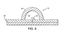
- FIG 7 is a top view of an array of LED light sources according to this invention.
- the LED light sources 10 are mounted on a circuit board 20 in a 5x5 array.
- the circuit board 20 is fitted with an electrical connector 15 for supplying power to the LED light sources.
- a cross-sectional illustration of one of the LED light sources 10 is shown in Figure 8 .
- the LED die 25 is mounted to the circuit board 20 and is covered by a phosphor-filled dome 30.
- the dome contains the 3-component phosphor blend.
- the space 35 between the LED die 25 and the dome 30 is preferably filled with a transparent silicone resin.
Landscapes
- Chemical & Material Sciences (AREA)
- Inorganic Chemistry (AREA)
- Engineering & Computer Science (AREA)
- Materials Engineering (AREA)
- Organic Chemistry (AREA)
- Led Device Packages (AREA)
- Luminescent Compositions (AREA)
Description
- This application claims the benefit of
U.S. Provisional Application No. 61/234,525, filed 8/17/2009 - This invention relates to lighting for photography and cinematography, especially to the use of light emitting diodes (LEDs) for these applications.
- Lighting for the film industry started with sunlight about the beginning of the last century and thereafter evolved through the carbon arc to a mix of incandescent lamps, medium arc high intensity discharge lamps (e.g., HMI), and more recently, fluorescent lighting. To a greater or lesser extent, these light sources all required large amounts of electric power and generate large amounts of heat that is undesirable during film production. High power consumption is an especially difficult problem for location production where a supply of electric power may be limited unless portable electric generating plants are made available which can increase the cost of production.
- In addition, the films that have been developed over the years have been standardized to a degree to have responses based on the spectral characteristics of specific light sources. In particular, two widely used films have based their responses on a incandescent 3200K tungsten source and a standard 5500 K daylight source as exemplified by KODAK Color Negative Film 5219 and KODAK Color Negative Film 5205, respectively. It is important therefore that any new light sources which might be developed for photography or cinematography have appropriate spectral power distributions for use with these films.
-
WO 2009/028657 A1 discloses a light emitting device comprising a light emitting element, a red phosphor, a green phosphor, and a YAG phosphor to emit white light. -
US 2007/0170842 A1 discloses an illumination device comprising at least one LED and three phosphors to convert partially or completely the emitted primary radiation of the LED so that white light is formed. -
US 2006/0214576 A1 discloses an electroluminescent display device including an electroluminescent light-emitting layer and a color conversion filter layer. - It is an object of the invention to obviate the disadvantages of the prior art.
- It is a another object of the invention to provide a light source based an LEDs with the major objectives of reducing heat in the vicinity of the light sources and, more importantly, reducing the power required to operate such lighting.
- It is a further object of the invention to provide a light source having a spectral power distribution appropriate for a 5500 K daylight balanced color film.
- In accordance with an aspect of the invention, there is provided a phosphor blend for an LED light source comprising from about 25 to about 35 weight percent of a cerium-activated yttrium aluminum garnet phosphor, from about 5 to about 10 weight percent of a europium-activated strontium calcium silicon nitride phosphor, and from about 50 to about 75 weight percent of a europium-activated calcium magnesium chlorosilicate phosphor.
- Preferably, the phosphor blend comprises from about 28 to about 32 weight percent of the cerium-activated yttrium aluminum garnet phosphor, from about 6 to about 8 weight percent of the europium-activated strontium calcium silicon nitride phosphor, and from about 60 to about 65 weight percent of the europium-activated calcium magnesium chlorosilicate phosphor.
- More preferably, the phosphor blend comprises about 30 weight percent of the cerium-activated yttrium aluminum garnet phosphor, about 7 weight percent of the europium-activated strontium calcium silicon nitride phosphor, and about 63 weight percent of the europium-activated calcium magnesium chlorosilicate phosphor.
- In accordance with another aspect of the invention, there is provided an LED light source including the phosphor blend, wherein the LED light source is configured to have a B:G:R ratio for a 5500 K daylight balanced color film of X:Y:Z when directly exposed through a nominal photographic lens, wherein X, Y and Z each have a value from 0.90 to 1.10.
-
-
Figure 1 illustrates the three film response sensitivities for 5500 K daylight film. -
Figure 2 shows the relative spectral power distribution of 5500 K reconstituted daylight. -
Figure 3 shows the average lens spectral transmittance used in the standard ANSI PH2.3-1972. -
Figure 4 shows a spectrum of an embodiment of an LED light source according to this invention for use with 5500 K daylight balanced color film. -
Figure 5 shows the chromaticity point of the LED light source on the 1931 CIE Chromaticity Diagram. -
Figure 6 shows the individual emission curves for the three phosphors comprising the phosphor blend according to this invention. -
Figure 7 is a top view of an array of LED light sources according to this invention. -
Figure 8 is a cross-sectional illustration of one of the LED light sources shown inFigure 7 . - In a preferred embodiment, the LED light source comprises either discrete LED elements or arrays of nominally identical elements that can be arranged in various ways to form a complete light source. The color quality as described by the spectral power distribution is balanced to satisfy the exposure requirements of 5500 K daylight balance film as exemplified by KODAK Color Negative Film 5205 although the LED source generally will function satisfactorily with other films nominally balanced for 5500 K daylight. The sine qua non is that non-selectively reflecting surfaces will be reproduced achromatically by the developed film. It will be noted that trichromatic films of this type cannot ever reproduce all possible colored reflective surfaces identically to their direct visual appearances irrespective of the light source spectral power distribution that is used. This well-known limitation is described in Kodak Publication No. E-73, Why a Color May Not Reproduce Correctly (312-10-78-DX, 1978).
- 5500 K daylight film is nominally balanced to give proper color reproduction with reconstituted daylight at a correlated color temperature (CIE 15:2004) of 5500 K. Reconstituted daylight (CIE 15:2004) is a form of averaged daylight expressed as a spectral power distribution. However, certain spectral power distributions that differ from this one can be made acceptable. Note that an acceptable alternative does not necessarily have to have a correlated color temperature of 5500 K. Regardless of the actual correlated color temperature of the LED source, it is identified as a 5500 K photographic light indicating that it is to be used with 5500 K daylight balanced film. Further, it is well-known that handheld photographic color temperature meters may not indicate either 5500 K or the actual correlated color temperature of the LED source. The light does not have to have any particular visual appearance in terms of color quality, and it does not have to meet any particular color quality metric for visual purposes. Parenthetically, we will note that the General Color Rendering Index (CIE 13.3-1995) of an acceptable light for this application commonly will fall in an acceptable range of values for commercial lighting lamps, i.e., roughly 70 or higher. The basic requirement is that the photographic system reproduces color in a proper and acceptable manner.
- The method for designing the light source is to control three metric values proportional to the three components of the film response when the film is directly exposed to the light source spectrum. The three components are called the blue (B), green (G), and red (R) responses because the three film component sensitivities fall in the regions of the spectrum that are so described.
Figure 1 illustrates the three film response sensitivities. We observe that the sensitivities of all three components are reasonably similar. -
Figure 2 shows the relative spectral power distribution of 5500 K reconstituted daylight. When this spectral power is independently weighted by each of the three spectral sensitivities, the resulting blue (B), green (G), and red (R) responses are proportional to the areas under the respective product curves. The necessary condition for the required achromatic reproduction of a non-selectively reflecting surface is that B:G:R is in the proportions of 1:1:1. This establishes the "white point" for the film exposure. We note that the spectral power of the 5500 K daylight is reasonably constant across the visible spectrum, a lack of variation that is similar to that of the areas under the three sensitivity curves versus wavelength. Clearly the balance of film sensitivities has been set to give three equal responses under a 5500 K daylight light source. - As an essential component of the computation for the desired light source spectral distribution, note that the blue sensitivity of the film extends below 400 nm into the ultraviolet region of the spectrum. If the design were to proceed with the inherent blue film sensitivity, nonvisible radiation would influence the white point balance. But we also note that photographic lenses attenuate short wavelength radiation to a greater or lesser extent in the ultraviolet and sometimes well into the violet and blue regions of the visible spectrum. The effect depends on the various glasses used in manufacturing of a particular photographic camera lens and on the various lens coatings commonly used to reduce surface reflections at the various glass surfaces within the lens. The best we can do when designing a photographic light source to be used with a particular film is to make an average correction that is reasonably representative for most lenses. In this instance, we select the average lens spectral transmittance that is used in the standard ANSI PH2.3-1972. This lens transmittance (see
Figure 3 ) greatly reduces the blue response of the film to UV in a light source. The product of the blue film sensitivity and the typical average lens transmittance results in an effective blue film response as shown by the dashed line inFigure 1 . It is this modified blue response that is used in the LED design process. If the lens transmittance did not attenuate in the visible spectrum, this would be a moot point for the LED system in which the LED system does not radiate in the ultraviolet. However, the attenuation in the blue end of the visible spectrum above 400 nm will affect the white point balance. - The final acceptance of an LED or most other types of light sources for photography and cinematography cannot be set by computational or measurement means. It anticipated and expected that each light will have minor and subtle effects on the film exposure. These only can be determined by film tests using the actual or typical scenes. The lighting director will look at the resulting photography and make a decision of acceptability. If it is not quite to his liking, a weak color compensating and/or light balancing filter will be placed in front of the light. At the same time another lighting director may prefer the light without the filter(s) rather than the light changed by the filter. Because this is an issue of human preference, we do not expect universal agreement on the exact characteristics of a preferred light. Other issues such as the variation of any particular lens from the average typical lens transmittance will have a small effect on the performance of the light interacting with the film response. Many other minor factors are known and controlled to a greater or lesser extent. Examples of such factors would be deviations in the particular batch of film stock, the developing process, nonlinearities in the photographic process, etc. Consequently, some small variation in the B:G:R ratio characterizing an acceptable light source is expected and will not be significant providing that it is not excessive. When making final evaluative judgments of the color balance, there may be small displacements in the target design ratio due to such factors as the blue cutoff of the actual lens used in the evaluation.
- What we have invented is a phosphor blend and an LED light source designed for use in conjunction with color film balanced for 5500 K average daylight. The ratio of the three color components of the film, B:G:R, when directly exposed through a nominal photographic lens, is 1:1:1. The acceptable variability for this invention is defined at ±20 % for each of the three numerical values. Preferably, the LED light source has a B:G:R ratio for a 5500 K daylight balanced color film of X:Y:Z when directly exposed through a nominal photographic lens, wherein X, Y and Z each have a value from 0.90 to 1.10.
-
Figure 4 shows an exemplary LED light source according to an embodiment of this invention for use with 5500 K daylight balanced color film. The B:G:R ratio is 1.00:1.13:1.03. While visible metrics are irrelevant for this invention in its intended application, such values may aid in visualizing this light source. The correlated color temperature is 5690 K while the general color rendering index is 93. In a preferred embodiment, the LED sources use blue-emitting LED chips with phosphor embedded domes that provide the full required spectral range. Blue-emitting LEDs with dominate wavelengths in the range of 455-465nm are typically used and the phosphor embedded domes contain a three-component blend of phosphors. - The three phosphor components in the blend include (1) a europium-activated calcium magnesium chlorosilicate phosphor, preferably having a composition represented by the formula, Ca8Mg(SiO4)4Cl2:Eu2+, and having a peak emission at about 500-510 nm; (2) a europium-activated strontium calcium silicon nitride phosphor, preferably having a composition represented by the formula, Sr2-xCaxSi5N8:Eu2+, and having a peak emission at about 655-665 nm; and (3) a cerium-activated yttrium aluminum garnet phosphor, preferably having a composition represented by the formula, Y3Al5O12:Ce3+, and having a peak emission at about 560-570 nm. The preferred phosphor blend in Table I was developed to couple with the spectral response of common daylight balanced films. Depending on the geometry of the part containing the phosphor blend (dome volume converted package) the concentration of the phosphor blend in the silicone matrix will vary. Typical values are 5-10 weight percent (wt%) phosphor blend in the silicone matrix.
Table I. Phosphor Wt% Phosphor dominant wavelength (nm) Y3Al5O12:Ce3+ 30.0 573 Sr2-xCaxSi5N8:Eu2+ 6.75 608 Ca8Mg(SiO4)4Cl2:Eu2+ 63.25 524 -
Figure 5 shows the chromaticity point of the LED light source on the 1931 CIE Chromaticity Diagram where correlated color temperature lines are labeled in kelvin. The chromaticity, the correlated color temperature, and the general color rendering index are not given tolerances because they are dependent variables; B, G, and R are the independent variables.Figure 6 shows the individual emission curves for the three phosphors comprising the blend. The phosphors are excited by the blue light emission from the blue LED and the light emitted by the phosphors combines with the remaining blue emission from the LED to produce the desired spectral output. -
Figure 7 is a top view of an array of LED light sources according to this invention. TheLED light sources 10 are mounted on acircuit board 20 in a 5x5 array. Thecircuit board 20 is fitted with anelectrical connector 15 for supplying power to the LED light sources. A cross-sectional illustration of one of theLED light sources 10 is shown inFigure 8 . The LED die 25 is mounted to thecircuit board 20 and is covered by a phosphor-filleddome 30. The dome contains the 3-component phosphor blend. Thespace 35 between the LED die 25 and thedome 30 is preferably filled with a transparent silicone resin. - While there have been shown and described what are at present considered to be preferred embodiments of the invention, it will be apparent to those skilled in the art that various changes and modifications can be made herein without departing from the scope of the invention as defined by the appended claims.
Claims (6)
- A phosphor blend for an LED light source (10) comprising from 25 to 35 weight percent of a cerium-activated yttrium aluminum garnet phosphor, from 5 to 10 weight percent of a europium-activated strontium calcium silicon nitride phosphor, and from 50 to 75 weight percent of a europium-activated calcium magnesium chlorosilicate phosphor.
- The phosphor blend of claim 1 wherein the blend comprises from 28 to 32 weight percent of the cerium-activated yttrium aluminum garnet phosphor, from 6 to 8 weight percent of the europium-activated strontium calcium silicon nitride phosphor, and from 60 to 65 weight percent of the europium-activated calcium magnesium chlorosilicate phosphor.
- The phosphor blend of claim 1 wherein the blend comprises 30 weight percent of the cerium-activated yttrium aluminum garnet phosphor, 7 weight percent of the europium-activated strontium calcium silicon nitride phosphor, and 63 weight percent of the europium-activated calcium magnesium chlorosilicate phosphor.
- The phosphor blend of claim 1 wherein the cerium-activated yttrium aluminum garnet phosphor has a composition represented by a formula Y3Al5012:Ce3+, the europium-activated strontium calcium silicon nitride phosphor has a composition represented by a formula, Sr2-xCaxSi5N8:Eu2+, and the europium-activated calcium magnesium chlorosilicate phosphor has a composition represented by a formula Ca8Mg(SiO4)4Cl2:Eu2+.
- An LED light source (10) comprising the phosphor blend of claim 1, wherein the LED light source (10) is configured to have a B:G:R ratio for a 5500 K daylight balanced color film of X:Y:Z when directly exposed through a nominal photographic lens, wherein X, Y and Z each have a value from 0.90 to 1.10.
- An LED light source (10) comprising the phosphor blend of claim 1, wherein the LED light source (10) is configured to have a B:G:R ratio for a 5500 K daylight balanced color film of 1.00:1.13:1.03 when directly exposed through a nominal photographic lens.
Applications Claiming Priority (2)
| Application Number | Priority Date | Filing Date | Title |
|---|---|---|---|
| US23452509P | 2009-08-17 | 2009-08-17 | |
| PCT/US2010/045760 WO2011022399A1 (en) | 2009-08-17 | 2010-08-17 | Phosphor blend for an led light source and led light source incorporating same |
Publications (2)
| Publication Number | Publication Date |
|---|---|
| EP2467448A1 EP2467448A1 (en) | 2012-06-27 |
| EP2467448B1 true EP2467448B1 (en) | 2016-03-23 |
Family
ID=43479472
Family Applications (1)
| Application Number | Title | Priority Date | Filing Date |
|---|---|---|---|
| EP10747362.1A Not-in-force EP2467448B1 (en) | 2009-08-17 | 2010-08-17 | Phosphor blend for an led light source and led light source incorporating same |
Country Status (3)
| Country | Link |
|---|---|
| US (1) | US8796715B2 (en) |
| EP (1) | EP2467448B1 (en) |
| WO (1) | WO2011022399A1 (en) |
Families Citing this family (4)
| Publication number | Priority date | Publication date | Assignee | Title |
|---|---|---|---|---|
| US8704440B2 (en) | 2011-07-06 | 2014-04-22 | Osram Sylvania Inc. | LED lighting device having a phosphor composition |
| DE102011113498A1 (en) * | 2011-09-15 | 2013-03-21 | Osram Opto Semiconductors Gmbh | Phosphor mixture, optoelectronic component with a phosphor mixture and street lamp with a phosphor mixture |
| DE102013113382A1 (en) * | 2013-12-03 | 2015-06-03 | Osram Gmbh | Phosphor mixture, semiconductor light-emitting device with a phosphor mixture and street lamp with a phosphor mixture |
| JP2015188050A (en) * | 2014-03-12 | 2015-10-29 | 株式会社東芝 | light-emitting device |
Family Cites Families (6)
| Publication number | Priority date | Publication date | Assignee | Title |
|---|---|---|---|---|
| DE10026435A1 (en) | 2000-05-29 | 2002-04-18 | Osram Opto Semiconductors Gmbh | Calcium-magnesium-chlorosilicate phosphor and its application in luminescence conversion LEDs |
| DE10036940A1 (en) | 2000-07-28 | 2002-02-07 | Patent Treuhand Ges Fuer Elektrische Gluehlampen Mbh | Luminescence conversion LED |
| JP2006269382A (en) | 2005-03-25 | 2006-10-05 | Fuji Photo Film Co Ltd | Electroluminescent display element |
| US8648523B2 (en) | 2007-08-30 | 2014-02-11 | Nichia Corporation | Light emitting device including light emitting element and phosphor |
| DE102007044556A1 (en) | 2007-09-07 | 2009-03-12 | Arnold & Richter Cine Technik Gmbh & Co. Betriebs Kg | Method and device for adjusting the color or photometric properties of an LED lighting device |
| EP2467449B1 (en) * | 2009-08-17 | 2014-11-26 | OSRAM SYLVANIA Inc. | Phosphor blend for a led light source and led light source incorporating same |
-
2010
- 2010-08-17 WO PCT/US2010/045760 patent/WO2011022399A1/en not_active Ceased
- 2010-08-17 US US13/388,953 patent/US8796715B2/en not_active Expired - Fee Related
- 2010-08-17 EP EP10747362.1A patent/EP2467448B1/en not_active Not-in-force
Also Published As
| Publication number | Publication date |
|---|---|
| WO2011022399A1 (en) | 2011-02-24 |
| EP2467448A1 (en) | 2012-06-27 |
| US8796715B2 (en) | 2014-08-05 |
| US20120126253A1 (en) | 2012-05-24 |
Similar Documents
| Publication | Publication Date | Title |
|---|---|---|
| US12245445B2 (en) | White light source including LED and phosphors | |
| US20220068893A1 (en) | Systems For Providing Tunable White Light with High Color Rendering | |
| JP5005712B2 (en) | Light emitting device | |
| JP2023058559A (en) | full spectrum white light emitting device | |
| US9070843B2 (en) | Semiconductor light-emitting device, exhibit-irradiating illumination device, meat-irradiating illumination device, vegetable-irradiating illumination device, fresh fish-irradiating illumination device, general-purpose illumination device, and semiconductor light-emitting system | |
| US9507200B2 (en) | Method of manufacturing image display device and method of selecting color filter | |
| JP2006173622A (en) | Light emitting diode flash module with improved emission spectrum | |
| JP2012191225A (en) | Light-emitting device | |
| CN102959312A (en) | Led light bulb | |
| EP2467448B1 (en) | Phosphor blend for an led light source and led light source incorporating same | |
| US8592829B2 (en) | Phosphor blend for an LED light source and LED light source incorporating same | |
| US10256374B2 (en) | Light emitting device | |
| KR100902988B1 (en) | Manufacturing method of white light emitting diode | |
| JP2014150293A (en) | Light-emitting device | |
| US20040032204A1 (en) | Method for manufacturing white light source | |
| CN109560180A (en) | Light emitting device | |
| US20250048802A1 (en) | Light-emitting device and light source device | |
| US7701124B2 (en) | White light-emitting device having a cap layer formed from a mixture of silicon and a phosphor blend | |
| US11211530B2 (en) | Light source and illumination device including the light source | |
| JP2020140810A (en) | Lighting device | |
| CN118160105A (en) | Light emitting device and light source device | |
| CN101769506B (en) | A method of making pure white light diode light source | |
| TWI396302B (en) | A method of making white light source with high color rendering index and high color gamut |
Legal Events
| Date | Code | Title | Description |
|---|---|---|---|
| PUAI | Public reference made under article 153(3) epc to a published international application that has entered the european phase |
Free format text: ORIGINAL CODE: 0009012 |
|
| 17P | Request for examination filed |
Effective date: 20120117 |
|
| AK | Designated contracting states |
Kind code of ref document: A1 Designated state(s): AL AT BE BG CH CY CZ DE DK EE ES FI FR GB GR HR HU IE IS IT LI LT LU LV MC MK MT NL NO PL PT RO SE SI SK SM TR |
|
| DAX | Request for extension of the european patent (deleted) | ||
| 17Q | First examination report despatched |
Effective date: 20130307 |
|
| REG | Reference to a national code |
Ref country code: DE Ref legal event code: R079 Ref document number: 602010031430 Country of ref document: DE Free format text: PREVIOUS MAIN CLASS: C09K0011770000 Ipc: H05B0033140000 |
|
| RIC1 | Information provided on ipc code assigned before grant |
Ipc: C09K 11/61 20060101ALI20150727BHEP Ipc: H05B 33/14 20060101AFI20150727BHEP Ipc: H01L 33/50 20100101ALI20150727BHEP Ipc: C09K 11/80 20060101ALI20150727BHEP Ipc: C09K 11/59 20060101ALI20150727BHEP |
|
| GRAP | Despatch of communication of intention to grant a patent |
Free format text: ORIGINAL CODE: EPIDOSNIGR1 |
|
| INTG | Intention to grant announced |
Effective date: 20150916 |
|
| GRAS | Grant fee paid |
Free format text: ORIGINAL CODE: EPIDOSNIGR3 |
|
| GRAA | (expected) grant |
Free format text: ORIGINAL CODE: 0009210 |
|
| AK | Designated contracting states |
Kind code of ref document: B1 Designated state(s): AL AT BE BG CH CY CZ DE DK EE ES FI FR GB GR HR HU IE IS IT LI LT LU LV MC MK MT NL NO PL PT RO SE SI SK SM TR |
|
| REG | Reference to a national code |
Ref country code: GB Ref legal event code: FG4D |
|
| REG | Reference to a national code |
Ref country code: CH Ref legal event code: EP |
|
| REG | Reference to a national code |
Ref country code: AT Ref legal event code: REF Ref document number: 784256 Country of ref document: AT Kind code of ref document: T Effective date: 20160415 |
|
| REG | Reference to a national code |
Ref country code: IE Ref legal event code: FG4D |
|
| REG | Reference to a national code |
Ref country code: DE Ref legal event code: R096 Ref document number: 602010031430 Country of ref document: DE |
|
| REG | Reference to a national code |
Ref country code: LT Ref legal event code: MG4D |
|
| REG | Reference to a national code |
Ref country code: NL Ref legal event code: MP Effective date: 20160323 |
|
| PG25 | Lapsed in a contracting state [announced via postgrant information from national office to epo] |
Ref country code: GR Free format text: LAPSE BECAUSE OF FAILURE TO SUBMIT A TRANSLATION OF THE DESCRIPTION OR TO PAY THE FEE WITHIN THE PRESCRIBED TIME-LIMIT Effective date: 20160624 Ref country code: FI Free format text: LAPSE BECAUSE OF FAILURE TO SUBMIT A TRANSLATION OF THE DESCRIPTION OR TO PAY THE FEE WITHIN THE PRESCRIBED TIME-LIMIT Effective date: 20160323 Ref country code: NO Free format text: LAPSE BECAUSE OF FAILURE TO SUBMIT A TRANSLATION OF THE DESCRIPTION OR TO PAY THE FEE WITHIN THE PRESCRIBED TIME-LIMIT Effective date: 20160623 Ref country code: HR Free format text: LAPSE BECAUSE OF FAILURE TO SUBMIT A TRANSLATION OF THE DESCRIPTION OR TO PAY THE FEE WITHIN THE PRESCRIBED TIME-LIMIT Effective date: 20160323 |
|
| REG | Reference to a national code |
Ref country code: AT Ref legal event code: MK05 Ref document number: 784256 Country of ref document: AT Kind code of ref document: T Effective date: 20160323 |
|
| PG25 | Lapsed in a contracting state [announced via postgrant information from national office to epo] |
Ref country code: SE Free format text: LAPSE BECAUSE OF FAILURE TO SUBMIT A TRANSLATION OF THE DESCRIPTION OR TO PAY THE FEE WITHIN THE PRESCRIBED TIME-LIMIT Effective date: 20160323 Ref country code: LV Free format text: LAPSE BECAUSE OF FAILURE TO SUBMIT A TRANSLATION OF THE DESCRIPTION OR TO PAY THE FEE WITHIN THE PRESCRIBED TIME-LIMIT Effective date: 20160323 Ref country code: NL Free format text: LAPSE BECAUSE OF FAILURE TO SUBMIT A TRANSLATION OF THE DESCRIPTION OR TO PAY THE FEE WITHIN THE PRESCRIBED TIME-LIMIT Effective date: 20160323 Ref country code: LT Free format text: LAPSE BECAUSE OF FAILURE TO SUBMIT A TRANSLATION OF THE DESCRIPTION OR TO PAY THE FEE WITHIN THE PRESCRIBED TIME-LIMIT Effective date: 20160323 |
|
| PG25 | Lapsed in a contracting state [announced via postgrant information from national office to epo] |
Ref country code: EE Free format text: LAPSE BECAUSE OF FAILURE TO SUBMIT A TRANSLATION OF THE DESCRIPTION OR TO PAY THE FEE WITHIN THE PRESCRIBED TIME-LIMIT Effective date: 20160323 Ref country code: PL Free format text: LAPSE BECAUSE OF FAILURE TO SUBMIT A TRANSLATION OF THE DESCRIPTION OR TO PAY THE FEE WITHIN THE PRESCRIBED TIME-LIMIT Effective date: 20160323 Ref country code: IS Free format text: LAPSE BECAUSE OF FAILURE TO SUBMIT A TRANSLATION OF THE DESCRIPTION OR TO PAY THE FEE WITHIN THE PRESCRIBED TIME-LIMIT Effective date: 20160723 |
|
| PG25 | Lapsed in a contracting state [announced via postgrant information from national office to epo] |
Ref country code: CZ Free format text: LAPSE BECAUSE OF FAILURE TO SUBMIT A TRANSLATION OF THE DESCRIPTION OR TO PAY THE FEE WITHIN THE PRESCRIBED TIME-LIMIT Effective date: 20160323 Ref country code: PT Free format text: LAPSE BECAUSE OF FAILURE TO SUBMIT A TRANSLATION OF THE DESCRIPTION OR TO PAY THE FEE WITHIN THE PRESCRIBED TIME-LIMIT Effective date: 20160725 Ref country code: SK Free format text: LAPSE BECAUSE OF FAILURE TO SUBMIT A TRANSLATION OF THE DESCRIPTION OR TO PAY THE FEE WITHIN THE PRESCRIBED TIME-LIMIT Effective date: 20160323 Ref country code: RO Free format text: LAPSE BECAUSE OF FAILURE TO SUBMIT A TRANSLATION OF THE DESCRIPTION OR TO PAY THE FEE WITHIN THE PRESCRIBED TIME-LIMIT Effective date: 20160323 Ref country code: ES Free format text: LAPSE BECAUSE OF FAILURE TO SUBMIT A TRANSLATION OF THE DESCRIPTION OR TO PAY THE FEE WITHIN THE PRESCRIBED TIME-LIMIT Effective date: 20160323 Ref country code: SM Free format text: LAPSE BECAUSE OF FAILURE TO SUBMIT A TRANSLATION OF THE DESCRIPTION OR TO PAY THE FEE WITHIN THE PRESCRIBED TIME-LIMIT Effective date: 20160323 Ref country code: AT Free format text: LAPSE BECAUSE OF FAILURE TO SUBMIT A TRANSLATION OF THE DESCRIPTION OR TO PAY THE FEE WITHIN THE PRESCRIBED TIME-LIMIT Effective date: 20160323 |
|
| PG25 | Lapsed in a contracting state [announced via postgrant information from national office to epo] |
Ref country code: BE Free format text: LAPSE BECAUSE OF FAILURE TO SUBMIT A TRANSLATION OF THE DESCRIPTION OR TO PAY THE FEE WITHIN THE PRESCRIBED TIME-LIMIT Effective date: 20160323 Ref country code: IT Free format text: LAPSE BECAUSE OF FAILURE TO SUBMIT A TRANSLATION OF THE DESCRIPTION OR TO PAY THE FEE WITHIN THE PRESCRIBED TIME-LIMIT Effective date: 20160323 |
|
| REG | Reference to a national code |
Ref country code: DE Ref legal event code: R097 Ref document number: 602010031430 Country of ref document: DE |
|
| PLBE | No opposition filed within time limit |
Free format text: ORIGINAL CODE: 0009261 |
|
| STAA | Information on the status of an ep patent application or granted ep patent |
Free format text: STATUS: NO OPPOSITION FILED WITHIN TIME LIMIT |
|
| PG25 | Lapsed in a contracting state [announced via postgrant information from national office to epo] |
Ref country code: DK Free format text: LAPSE BECAUSE OF FAILURE TO SUBMIT A TRANSLATION OF THE DESCRIPTION OR TO PAY THE FEE WITHIN THE PRESCRIBED TIME-LIMIT Effective date: 20160323 |
|
| PG25 | Lapsed in a contracting state [announced via postgrant information from national office to epo] |
Ref country code: BG Free format text: LAPSE BECAUSE OF FAILURE TO SUBMIT A TRANSLATION OF THE DESCRIPTION OR TO PAY THE FEE WITHIN THE PRESCRIBED TIME-LIMIT Effective date: 20160623 |
|
| 26N | No opposition filed |
Effective date: 20170102 |
|
| PG25 | Lapsed in a contracting state [announced via postgrant information from national office to epo] |
Ref country code: MC Free format text: LAPSE BECAUSE OF FAILURE TO SUBMIT A TRANSLATION OF THE DESCRIPTION OR TO PAY THE FEE WITHIN THE PRESCRIBED TIME-LIMIT Effective date: 20160323 |
|
| REG | Reference to a national code |
Ref country code: CH Ref legal event code: PL |
|
| GBPC | Gb: european patent ceased through non-payment of renewal fee |
Effective date: 20160817 |
|
| PG25 | Lapsed in a contracting state [announced via postgrant information from national office to epo] |
Ref country code: CH Free format text: LAPSE BECAUSE OF NON-PAYMENT OF DUE FEES Effective date: 20160831 Ref country code: LI Free format text: LAPSE BECAUSE OF NON-PAYMENT OF DUE FEES Effective date: 20160831 |
|
| REG | Reference to a national code |
Ref country code: FR Ref legal event code: ST Effective date: 20170428 |
|
| PG25 | Lapsed in a contracting state [announced via postgrant information from national office to epo] |
Ref country code: SI Free format text: LAPSE BECAUSE OF FAILURE TO SUBMIT A TRANSLATION OF THE DESCRIPTION OR TO PAY THE FEE WITHIN THE PRESCRIBED TIME-LIMIT Effective date: 20160323 |
|
| REG | Reference to a national code |
Ref country code: IE Ref legal event code: MM4A |
|
| PG25 | Lapsed in a contracting state [announced via postgrant information from national office to epo] |
Ref country code: IE Free format text: LAPSE BECAUSE OF NON-PAYMENT OF DUE FEES Effective date: 20160817 Ref country code: GB Free format text: LAPSE BECAUSE OF NON-PAYMENT OF DUE FEES Effective date: 20160817 Ref country code: FR Free format text: LAPSE BECAUSE OF NON-PAYMENT OF DUE FEES Effective date: 20160831 |
|
| PG25 | Lapsed in a contracting state [announced via postgrant information from national office to epo] |
Ref country code: LU Free format text: LAPSE BECAUSE OF NON-PAYMENT OF DUE FEES Effective date: 20160817 |
|
| PGFP | Annual fee paid to national office [announced via postgrant information from national office to epo] |
Ref country code: DE Payment date: 20170822 Year of fee payment: 8 |
|
| PG25 | Lapsed in a contracting state [announced via postgrant information from national office to epo] |
Ref country code: HU Free format text: LAPSE BECAUSE OF FAILURE TO SUBMIT A TRANSLATION OF THE DESCRIPTION OR TO PAY THE FEE WITHIN THE PRESCRIBED TIME-LIMIT; INVALID AB INITIO Effective date: 20100817 Ref country code: CY Free format text: LAPSE BECAUSE OF FAILURE TO SUBMIT A TRANSLATION OF THE DESCRIPTION OR TO PAY THE FEE WITHIN THE PRESCRIBED TIME-LIMIT Effective date: 20160323 |
|
| PG25 | Lapsed in a contracting state [announced via postgrant information from national office to epo] |
Ref country code: MK Free format text: LAPSE BECAUSE OF FAILURE TO SUBMIT A TRANSLATION OF THE DESCRIPTION OR TO PAY THE FEE WITHIN THE PRESCRIBED TIME-LIMIT Effective date: 20160323 Ref country code: TR Free format text: LAPSE BECAUSE OF FAILURE TO SUBMIT A TRANSLATION OF THE DESCRIPTION OR TO PAY THE FEE WITHIN THE PRESCRIBED TIME-LIMIT Effective date: 20160323 Ref country code: MT Free format text: LAPSE BECAUSE OF NON-PAYMENT OF DUE FEES Effective date: 20160831 |
|
| PG25 | Lapsed in a contracting state [announced via postgrant information from national office to epo] |
Ref country code: AL Free format text: LAPSE BECAUSE OF FAILURE TO SUBMIT A TRANSLATION OF THE DESCRIPTION OR TO PAY THE FEE WITHIN THE PRESCRIBED TIME-LIMIT Effective date: 20160323 |
|
| REG | Reference to a national code |
Ref country code: DE Ref legal event code: R119 Ref document number: 602010031430 Country of ref document: DE |
|
| PG25 | Lapsed in a contracting state [announced via postgrant information from national office to epo] |
Ref country code: DE Free format text: LAPSE BECAUSE OF NON-PAYMENT OF DUE FEES Effective date: 20190301 |