EP2467002A2 - Electronic component on-substrate mounting structure - Google Patents
Electronic component on-substrate mounting structure Download PDFInfo
- Publication number
- EP2467002A2 EP2467002A2 EP11194069A EP11194069A EP2467002A2 EP 2467002 A2 EP2467002 A2 EP 2467002A2 EP 11194069 A EP11194069 A EP 11194069A EP 11194069 A EP11194069 A EP 11194069A EP 2467002 A2 EP2467002 A2 EP 2467002A2
- Authority
- EP
- European Patent Office
- Prior art keywords
- electronic component
- substrate
- lead
- main body
- mounting structure
- Prior art date
- Legal status (The legal status is an assumption and is not a legal conclusion. Google has not performed a legal analysis and makes no representation as to the accuracy of the status listed.)
- Withdrawn
Links
Images


Classifications
-
- H—ELECTRICITY
- H05—ELECTRIC TECHNIQUES NOT OTHERWISE PROVIDED FOR
- H05K—PRINTED CIRCUITS; CASINGS OR CONSTRUCTIONAL DETAILS OF ELECTRIC APPARATUS; MANUFACTURE OF ASSEMBLAGES OF ELECTRICAL COMPONENTS
- H05K3/00—Apparatus or processes for manufacturing printed circuits
- H05K3/30—Assembling printed circuits with electric components, e.g. with resistor
- H05K3/306—Lead-in-hole components, e.g. affixing or retention before soldering, spacing means
- H05K3/308—Adaptations of leads
-
- H—ELECTRICITY
- H05—ELECTRIC TECHNIQUES NOT OTHERWISE PROVIDED FOR
- H05K—PRINTED CIRCUITS; CASINGS OR CONSTRUCTIONAL DETAILS OF ELECTRIC APPARATUS; MANUFACTURE OF ASSEMBLAGES OF ELECTRICAL COMPONENTS
- H05K2201/00—Indexing scheme relating to printed circuits covered by H05K1/00
- H05K2201/10—Details of components or other objects attached to or integrated in a printed circuit board
- H05K2201/10613—Details of electrical connections of non-printed components, e.g. special leads
- H05K2201/10621—Components characterised by their electrical contacts
- H05K2201/10651—Component having two leads, e.g. resistor, capacitor
-
- H—ELECTRICITY
- H05—ELECTRIC TECHNIQUES NOT OTHERWISE PROVIDED FOR
- H05K—PRINTED CIRCUITS; CASINGS OR CONSTRUCTIONAL DETAILS OF ELECTRIC APPARATUS; MANUFACTURE OF ASSEMBLAGES OF ELECTRICAL COMPONENTS
- H05K2201/00—Indexing scheme relating to printed circuits covered by H05K1/00
- H05K2201/10—Details of components or other objects attached to or integrated in a printed circuit board
- H05K2201/10613—Details of electrical connections of non-printed components, e.g. special leads
- H05K2201/10742—Details of leads
- H05K2201/1075—Shape details
- H05K2201/10757—Bent leads
-
- H—ELECTRICITY
- H05—ELECTRIC TECHNIQUES NOT OTHERWISE PROVIDED FOR
- H05K—PRINTED CIRCUITS; CASINGS OR CONSTRUCTIONAL DETAILS OF ELECTRIC APPARATUS; MANUFACTURE OF ASSEMBLAGES OF ELECTRICAL COMPONENTS
- H05K2201/00—Indexing scheme relating to printed circuits covered by H05K1/00
- H05K2201/10—Details of components or other objects attached to or integrated in a printed circuit board
- H05K2201/10613—Details of electrical connections of non-printed components, e.g. special leads
- H05K2201/10742—Details of leads
- H05K2201/1075—Shape details
- H05K2201/1078—Leads having locally deformed portion, e.g. for retention
-
- H—ELECTRICITY
- H05—ELECTRIC TECHNIQUES NOT OTHERWISE PROVIDED FOR
- H05K—PRINTED CIRCUITS; CASINGS OR CONSTRUCTIONAL DETAILS OF ELECTRIC APPARATUS; MANUFACTURE OF ASSEMBLAGES OF ELECTRICAL COMPONENTS
- H05K3/00—Apparatus or processes for manufacturing printed circuits
- H05K3/30—Assembling printed circuits with electric components, e.g. with resistor
- H05K3/32—Assembling printed circuits with electric components, e.g. with resistor electrically connecting electric components or wires to printed circuits
- H05K3/34—Assembling printed circuits with electric components, e.g. with resistor electrically connecting electric components or wires to printed circuits by soldering
- H05K3/3447—Lead-in-hole components
Definitions
- the present invention relates to a mounting structure for mounting an electronic component on a substrate.
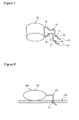
- an on-substrate mounting structure As shown in Fig. 8 , if a tall electronic component 100 is mounted on a substrate 110, then an electronic component main body 101 is arranged so that a longitudinal direction of the electronic component main body 101 is parallel to the substrate 110, and a lead 102 extending laterally from the electronic component main body 101 is bent and inserted into a lead hole 111 of the substrate 110, thereby making an overall height of the electronic component main body 101 small (see, for example, Patent Literature 1).
- Patent Literature 1 JPAHeisei 11-163493 (Claim 1; Page 2, right column; and Figs. 1 and 2 )
- the electronic component on-substrate mounting structure described in JPA Heisei 11-163493 has the following problems. As shown in Fig. 9 , if the electronic component 100 having a round external shape such as an electrolytic capacitor or a film capacitor is mounted on the substrate 110 with a round portion thereof opposing the substrate 110, problems occur such as one that the round external portion of the electronic component main body 101 abuts the substrate 110 and the electronic component main body 101 is arranged in an inclined attitude. Due to this, the electronic component 100 cannot be kept in a predetermined attitude.
- the electronic component main body 101 often differs in a thickness in a width direction of the electronic component main body 101 for reasons such as a change in finished dimensions of the electronic component main body 101.
- dimensions L of an allowance of the lead 102 protruding to a rear side of the substrate 110 become possibly excessively large.
- the present invention is an electronic component on-substrate mounting structure for mounting an electronic component on a substrate by inserting a lead of the electronic component into a lead hole of the substrate, wherein the lead includes: a base part extending from the electronic component main body; a support part supporting the electronic component by abutting on an electronic-component mount surface of the substrate at a predetermined length; and an insertion part bent from the support part, and inserted into the lead hole of the substrate.
- two or more leads are provided on the electronic component main body.
- the lead is bent three to six times.
- an allowance protruding from a surface of the substrate opposite to the electronic-component mount surface of the substrate is provided on a tip end of the insertion part of the lead, the allowance being bent toward a side of the lead opposite to the base part of the lead.
- a length of the insertion part of the lead is set according to a thickness of the substrate.
- the support part of the lead can support the electronic component main body in a predetermined attitude with respect to the substrate. It is also possible to suppress the allowance of the lead from becoming excessively large in dimensions.
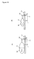
- FIG. 1 shows an electronic component on-substrate mounting structure 10 according to the embodiment of the present invention.
- This electronic component on-substrate mounting structure 10 is configured to mount an electronic component 11 on a substrate 30 by inserting and soldering a lead 12 of the electronic component 11 into a lead hole 31 of the substrate 20.
- An electronic component main body 13 of the electronic component 11 is, for example, one having a round external shape such as an electrolytic capacitor or a film capacitor.
- examples of the electronic component main body 13 possibly include one having a non-round external shape.
- the electronic component main body 13 is formed into an elliptical shape and mounted on the substrate 30 so that a longitudinal direction of the electronic component main body 13 is parallel to the substrate 30. By doing so, the round portion of the electronic component main body 13 is arranged to oppose the substrate 30.
- the lead 12 of the electronic component 11 is obtained by lead forming.
- the lead 12 is bent three times each at an angle of about 90 degrees.
- the lead 12 includes a base part 16 extending from one longitudinal end of the electronic component main body 13 in a longitudinal direction, a support part 17 bent twice each at an angle of about 90 degrees from a tip end of the base part 16 and supporting the electronic component main body 13 by causing a linear portion on a tip end side of the support part 17 to abut an electronic-component mount surface 30A of the substrate 30 at a predetermined length W, and an insertion part 18 bent once at an angle of about 90 degrees from a tip end of the support part 17 and inserted and soldered into the lead hole 31 of the substrate 30.
- an allowance 19 protruding to a rear side of the substrate 30 is provided on a tip end side of the insertion part 18.
- the insertion part 18 and the allowance 19 are formed almost linearly.
- the support part 17 of the lead 12 abuts the electronic-component mount surface 30A of the substrate 30 at the predetermined length W. It is, therefore, possible to support the electronic component main body 13 at a predetermined distance from the substrate 30 and in a predetermined attitude, which is, in this embodiment, a state of making the longitudinal direction of the electronic component main body 13 parallel to the substrate 30. Due to this, even if the electronic component main body 13 is tall, it is possible to make an overall height of the electronic component body 13 small.
- the support part 17 and the insertion part 18 are bent at 90 degrees with respect to each other. Due to this, even if the electronic component main body 13 inclines with respect to the predetermined attitude, it is possible to avoid inserting the support part 17 into the lead hole 31 of the substrate 30. Therefore, even if a width of the electronic component main body 13 in a direction orthogonal to the longitudinal direction thereof changes for such a reason as a change in finished dimensions of the electronic component main body 13, it is possible to suppress the allowance 19 of the lead 12 from becoming excessively large in dimensions.
- the present invention is also applicable to an electronic component 20 or 22 having, for example, two leads 12 extending from an electronic component main body 21 or 23.
- the electronic component 20 or 22 can be supported more stably.
- Fig. 3 shows an electronic component on-substrate mounting structure according to a modification of the embodiment.
- an allowance 41 bent at about 45 degrees from a tip end of the insertion part 18 of the lead 12, protruding from a surface opposite to the electronic component main body 13, and extending to a side opposite to the electronic component main body 13 is provided.
- a length of the insertion part 18 is set according to a thickness T of the substrate 30. In this example, the length of the insertion part 18 is set almost equal to the thickness T of the substrate 30.
- the allowance 19 of the lead 12 is caught in the substrate 30 when a force in a direction of separating from the substrate 30 acts on the electronic component main body 13. Therefore, it is possible to suppress the lead 12 from falling out of the lead hole 31.
- the length of the insertion part 18 is set according to the thickness T of the substrate 30, which means, in this modification, set almost equal to the thickness T.
- the electronic component 11 can be, therefore, stably mounted on the substrate 30.
- the electronic component 11 can be mounted on the substrate 30 in a state in which the electronic component main body 13 is apart from the electronic-component mount surface 30A of the substrate 30. Further, the electronic component 11 can be mounted on the substrate 30 in a state in which the electronic component main body 13 abuts the electronic-component mount surface 30A.
- the base part 16, the support part 17, the insertion part 18, and the allowance 19 can be provided. It is thereby possible to form the lead 12 suited for a mounted state or the like of the electronic component 25 without greatly increasing the number of machining times.
- the base part 16 to the allowance 19 can be provided by bending the lead 12 seven or more times.
Landscapes
- Engineering & Computer Science (AREA)
- Manufacturing & Machinery (AREA)
- Microelectronics & Electronic Packaging (AREA)
- Structures For Mounting Electric Components On Printed Circuit Boards (AREA)
Abstract
Description
- The present invention relates to a mounting structure for mounting an electronic component on a substrate.
- There is conventionally proposed an on-substrate mounting structure. As shown in
Fig. 8 , if a tallelectronic component 100 is mounted on asubstrate 110, then an electronic componentmain body 101 is arranged so that a longitudinal direction of the electronic componentmain body 101 is parallel to thesubstrate 110, and alead 102 extending laterally from the electronic componentmain body 101 is bent and inserted into alead hole 111 of thesubstrate 110, thereby making an overall height of the electronic componentmain body 101 small (see, for example, Patent Literature 1). - [Patent Literature 1] JPAHeisei 11-163493 (Claim 1; Page 2, right column; and
Figs. 1 and2 ) - However, the electronic component on-substrate mounting structure described in JPA Heisei 11-163493 has the following problems. As shown in
Fig. 9 , if theelectronic component 100 having a round external shape such as an electrolytic capacitor or a film capacitor is mounted on thesubstrate 110 with a round portion thereof opposing thesubstrate 110, problems occur such as one that the round external portion of the electronic componentmain body 101 abuts thesubstrate 110 and the electronic componentmain body 101 is arranged in an inclined attitude. Due to this, theelectronic component 100 cannot be kept in a predetermined attitude. - Furthermore, as shown in
Figs. 10(A) and 10(B) , the electronic componentmain body 101 often differs in a thickness in a width direction of the electronic componentmain body 101 for reasons such as a change in finished dimensions of the electronic componentmain body 101. In this case, as shown inFig. 10(B) , dimensions L of an allowance of thelead 102 protruding to a rear side of thesubstrate 110 become possibly excessively large. - If the allowance of the
lead 102 is excessively large in dimensions, problems such as one that the allowance of thelead 102 is caught in a nozzle of a tank and one that a sufficient insulation distance of theelectronic component 100 to a case (not shown) containing theelectronic component 100 cannot be kept possibly occur. - It is an object of the present invention to provide an on-substrate mounting structure for an electronic component capable of supporting an electronic component main body in a predetermined attitude and suppressing an allowance of a lead from becoming excessively large in dimensions even if the electronic component is mounted on a substrate with a round portion of the electronic component opposing the substrate.
- The present invention is an electronic component on-substrate mounting structure for mounting an electronic component on a substrate by inserting a lead of the electronic component into a lead hole of the substrate, wherein the lead includes: a base part extending from the electronic component main body; a support part supporting the electronic component by abutting on an electronic-component mount surface of the substrate at a predetermined length; and an insertion part bent from the support part, and inserted into the lead hole of the substrate.
- According to the present invention, two or more leads are provided on the electronic component main body.
- According to the present invention, the lead is bent three to six times.
- According to the present invention, an allowance protruding from a surface of the substrate opposite to the electronic-component mount surface of the substrate is provided on a tip end of the insertion part of the lead, the allowance being bent toward a side of the lead opposite to the base part of the lead.
- According to the present invention, a length of the insertion part of the lead is set according to a thickness of the substrate.
- According to the present invention, even if the electronic component is mounted on the substrate with the round portion of the electronic component opposing the substrate, the support part of the lead can support the electronic component main body in a predetermined attitude with respect to the substrate. It is also possible to suppress the allowance of the lead from becoming excessively large in dimensions.
-
- [
Fig.1] Fig. 1 is a partially cross-sectional front view showing an electronic component on-substrate mounting structure according to an embodiment of the present invention. - [
Fig.2] Figs. 2(A) and 2(B) are perspective views showing other types of leads according to the embodiment. - [
Fig.3] Fig. 3 is a partially cross-sectional front view showing a modification of the embodiment. - [
Fig.4] Fig. 4 is a partially cross-sectional front view showing another modification of the embodiment. - [
Fig.5] Fig. 5 is a perspective view showing two leads each having a support part and the like provided by being bent four times. - [
Fig.6] Fig. 6 is a perspective view showing two leads each having a support part and the like provided by being bent five times. - [
Fig.7] Fig. 7 is a perspective view showing two leads each having a support part and the like provided by being bent six times. - [
Fig.8] Fig. 8 is a partially cross-sectional front view showing an electronic component on-substrate mounting structure according to a conventional technique. - [
Fig.9] Fig. 9 is a partially cross-sectional front view showing a state in which an electronic component is inclined with respect to a predetermined attitude according to the conventional technique. - [
Fig.10] Fig. 10(A) shows a mounted state if the electronic component has normal finished dimensions according to the conventional technique, andFig. 10(B) shows a mounted state if the electronic component has excessively small dimensions according to the conventional technique. - An electronic component on-substrate mounting structure according to an embodiment of the present invention will be described hereinafter with reference to the drawings.
Fig. 1 shows an electronic component on-substrate mounting structure 10 according to the embodiment of the present invention. This electronic component on-substrate mounting structure 10 is configured to mount anelectronic component 11 on asubstrate 30 by inserting and soldering alead 12 of theelectronic component 11 into alead hole 31 of thesubstrate 20. - An electronic component
main body 13 of theelectronic component 11 is, for example, one having a round external shape such as an electrolytic capacitor or a film capacitor. However, examples of the electronic componentmain body 13 possibly include one having a non-round external shape. In the present embodiment, the electronic componentmain body 13 is formed into an elliptical shape and mounted on thesubstrate 30 so that a longitudinal direction of the electronic componentmain body 13 is parallel to thesubstrate 30. By doing so, the round portion of the electronic componentmain body 13 is arranged to oppose thesubstrate 30. - The
lead 12 of theelectronic component 11 is obtained by lead forming. In this example, thelead 12 is bent three times each at an angle of about 90 degrees. By doing so, thelead 12 includes abase part 16 extending from one longitudinal end of the electronic componentmain body 13 in a longitudinal direction, asupport part 17 bent twice each at an angle of about 90 degrees from a tip end of thebase part 16 and supporting the electronic componentmain body 13 by causing a linear portion on a tip end side of thesupport part 17 to abut an electronic-component mount surface 30A of thesubstrate 30 at a predetermined length W, and aninsertion part 18 bent once at an angle of about 90 degrees from a tip end of thesupport part 17 and inserted and soldered into thelead hole 31 of thesubstrate 30. - In this example, an
allowance 19 protruding to a rear side of thesubstrate 30 is provided on a tip end side of theinsertion part 18. In this example, theinsertion part 18 and theallowance 19 are formed almost linearly. - According to this electronic component on-
substrate mounting structure 10, thesupport part 17 of thelead 12 abuts the electronic-component mount surface 30A of thesubstrate 30 at the predetermined length W. It is, therefore, possible to support the electronic componentmain body 13 at a predetermined distance from thesubstrate 30 and in a predetermined attitude, which is, in this embodiment, a state of making the longitudinal direction of the electronic componentmain body 13 parallel to thesubstrate 30. Due to this, even if the electronic componentmain body 13 is tall, it is possible to make an overall height of theelectronic component body 13 small. - Furthermore, the
support part 17 and theinsertion part 18 are bent at 90 degrees with respect to each other. Due to this, even if the electronic componentmain body 13 inclines with respect to the predetermined attitude, it is possible to avoid inserting thesupport part 17 into thelead hole 31 of thesubstrate 30. Therefore, even if a width of the electronic componentmain body 13 in a direction orthogonal to the longitudinal direction thereof changes for such a reason as a change in finished dimensions of the electronic componentmain body 13, it is possible to suppress theallowance 19 of thelead 12 from becoming excessively large in dimensions. - As shown in
Figs. 2(A) and 2(B) , the present invention is also applicable to anelectronic component 20 or 22 having, for example, two leads 12 extending from an electronic componentmain body electronic component 20 or 22 can be supported more stably. -
Fig. 3 shows an electronic component on-substrate mounting structure according to a modification of the embodiment. - Elements that are the same as those in
Fig. 1 are denoted by the same reference numerals and not described herein. In an electronic component on-substrate mounting structure 40, anallowance 41 bent at about 45 degrees from a tip end of theinsertion part 18 of thelead 12, protruding from a surface opposite to the electronic componentmain body 13, and extending to a side opposite to the electronic componentmain body 13 is provided. A length of theinsertion part 18 is set according to a thickness T of thesubstrate 30. In this example, the length of theinsertion part 18 is set almost equal to the thickness T of thesubstrate 30. - According to this electronic component on-
substrate mounting structure 40, theallowance 19 of thelead 12 is caught in thesubstrate 30 when a force in a direction of separating from thesubstrate 30 acts on the electronic componentmain body 13. Therefore, it is possible to suppress thelead 12 from falling out of thelead hole 31. - Furthermore, since the length of the
insertion part 18 is set according to the thickness T of thesubstrate 30, which means, in this modification, set almost equal to the thickness T. Theelectronic component 11 can be, therefore, stably mounted on thesubstrate 30. - Moreover, as shown in
Fig. 4 , theelectronic component 11 can be mounted on thesubstrate 30 in a state in which the electronic componentmain body 13 is apart from the electronic-component mount surface 30A of thesubstrate 30. Further, theelectronic component 11 can be mounted on thesubstrate 30 in a state in which the electronic componentmain body 13 abuts the electronic-component mount surface 30A. - Furthermore, as shown in
Figs. 5 to 7 , by bending thelead 12 of anelectronic component 25 four or sixth times, thebase part 16, thesupport part 17, theinsertion part 18, and theallowance 19 can be provided. It is thereby possible to form thelead 12 suited for a mounted state or the like of theelectronic component 25 without greatly increasing the number of machining times.
Alternatively, thebase part 16 to theallowance 19 can be provided by bending the lead 12 seven or more times. -
- 10
- On-substrate mounting structure
- 11
- Electronic component
- 12
- Lead
- 13
- Electronic component main body
- 16
- Base part
- 17
- Support part
- 18
- Insertion part
- 19
- Allowance
- 20
- Electronic component
- 21
- Electronic component main body
- 25
- Electronic component
- 30
- Substrate
- 30A
- Electronic-component mount surface
- 31
- Lead hole
- 40
- Electronic component on-substrate mounting structure
- 41
- Allowance
- 100
- Electronic component
- 101
- Electronic component main body
- 102
- Lead
- 110
- Substrate
- 111
- Lead hole
Claims (5)
- An electronic component on-substrate mounting structure for mounting an electronic component on a substrate by inserting a lead of the electronic component into a lead hole of the substrate, wherein
the lead includes:a base part extending from the electronic component main body;a support part supporting the electronic component by abutting on an electronic-component mount surface of the substrate at a predetermined length; andan insertion part bent from the support part, and inserted into the lead hole of the substrate. - The electronic component on-substrate mounting structure according to claim 1, wherein
two or more leads are provided on the electronic component main body. - The electronic component on-substrate mounting structure according to claim 1 or 2, wherein
the lead is bent three to six times. - The electronic component on-substrate mounting structure according to claim 3, wherein
an allowance protruding to a surface of the substrate opposite to the electronic-component mount surface of the substrate is provided in the insertion part of the lead, the allowance being bent toward a side of the lead opposite to the base part of the lead. - The electronic component on-substrate mounting structure according to claim 4, wherein
a length of the insertion part of the lead is set according to a thickness of the substrate.
Applications Claiming Priority (1)
| Application Number | Priority Date | Filing Date | Title |
|---|---|---|---|
| JP2010283149A JP2012134224A (en) | 2010-12-20 | 2010-12-20 | Structure of attaching electronic component to board |
Publications (2)
| Publication Number | Publication Date |
|---|---|
| EP2467002A2 true EP2467002A2 (en) | 2012-06-20 |
| EP2467002A3 EP2467002A3 (en) | 2013-01-09 |
Family
ID=45442869
Family Applications (1)
| Application Number | Title | Priority Date | Filing Date |
|---|---|---|---|
| EP11194069A Withdrawn EP2467002A3 (en) | 2010-12-20 | 2011-12-16 | Electronic component on-substrate mounting structure |
Country Status (2)
| Country | Link |
|---|---|
| EP (1) | EP2467002A3 (en) |
| JP (1) | JP2012134224A (en) |
Cited By (1)
| Publication number | Priority date | Publication date | Assignee | Title |
|---|---|---|---|---|
| ITUA20162978A1 (en) * | 2016-04-28 | 2017-10-28 | Taco Italia S R L | Electronic control card for a circulator for a hydraulic system |
Citations (1)
| Publication number | Priority date | Publication date | Assignee | Title |
|---|---|---|---|---|
| JPH11163493A (en) | 1997-12-02 | 1999-06-18 | Funai Electric Co Ltd | Component mounting structure on board |
Family Cites Families (11)
| Publication number | Priority date | Publication date | Assignee | Title |
|---|---|---|---|---|
| JPS5327450U (en) * | 1976-08-16 | 1978-03-08 | ||
| JPS57155663U (en) * | 1981-03-27 | 1982-09-30 | ||
| US4541034A (en) * | 1984-04-26 | 1985-09-10 | At&T Technologies, Inc. | Electrical terminal and method of securing same in circuit substrate thru-hole |
| DE3625238A1 (en) * | 1985-07-31 | 1987-02-12 | Murata Manufacturing Co | ELECTRONIC COMPONENT WITH CONNECTING WIRE AND METHOD FOR PRODUCING THIS COMPONENT |
| JPS6316478U (en) * | 1986-07-18 | 1988-02-03 | ||
| US4763227A (en) * | 1987-08-03 | 1988-08-09 | Sprague Electric Company | Aluminum electrolytic capacitor package with stabilizing third lead |
| JPH03124010A (en) * | 1989-10-08 | 1991-05-27 | Murata Mfg Co Ltd | Terminal of electronic component |
| JPH0513126A (en) * | 1991-06-28 | 1993-01-22 | Nec Corp | Connector |
| JPH07176446A (en) * | 1993-12-20 | 1995-07-14 | Murata Mfg Co Ltd | Electronic component with lead terminal |
| JP2004119220A (en) * | 2002-09-26 | 2004-04-15 | Daishinku Corp | Method for manufacturing electronic part having leads, and electronic component having leads formed by the method |
| US20090161333A1 (en) * | 2007-12-19 | 2009-06-25 | Kevin Yang | Auto-cling leads of electric device |
-
2010
- 2010-12-20 JP JP2010283149A patent/JP2012134224A/en active Pending
-
2011
- 2011-12-16 EP EP11194069A patent/EP2467002A3/en not_active Withdrawn
Patent Citations (1)
| Publication number | Priority date | Publication date | Assignee | Title |
|---|---|---|---|---|
| JPH11163493A (en) | 1997-12-02 | 1999-06-18 | Funai Electric Co Ltd | Component mounting structure on board |
Cited By (1)
| Publication number | Priority date | Publication date | Assignee | Title |
|---|---|---|---|---|
| ITUA20162978A1 (en) * | 2016-04-28 | 2017-10-28 | Taco Italia S R L | Electronic control card for a circulator for a hydraulic system |
Also Published As
| Publication number | Publication date |
|---|---|
| EP2467002A3 (en) | 2013-01-09 |
| JP2012134224A (en) | 2012-07-12 |
Similar Documents
| Publication | Publication Date | Title |
|---|---|---|
| US9306297B2 (en) | Interlocking poke home contact | |
| US7695285B2 (en) | Spring connector and connector | |
| EP3146811B1 (en) | Printed circuit board arrangement | |
| JP5912632B2 (en) | connector | |
| EP2869402A1 (en) | Electrical connector and female terminal | |
| JP6084133B2 (en) | connector | |
| EP3007276A1 (en) | Caged poke home contact | |
| US20070173134A1 (en) | Fixing member and fixing structure | |
| JP4709502B2 (en) | Board mounted electrical connector | |
| EP2467002A2 (en) | Electronic component on-substrate mounting structure | |
| EP2966733A1 (en) | Connector | |
| JP4492799B2 (en) | Press fit pin | |
| US9022802B2 (en) | Terminal module | |
| JP2014236564A (en) | Bus bar | |
| EP2890226B1 (en) | Connection structure for substrate connector and connection method | |
| US7704090B2 (en) | Housing for a card edge connector assembly | |
| JP2010225446A (en) | Connecting terminal | |
| EP3879636A1 (en) | Contact | |
| EP2575215A1 (en) | Terminal fitting | |
| JP6053640B2 (en) | Board connector structure | |
| US9276337B2 (en) | Dynamically stable surface mount post header | |
| JP5449073B2 (en) | Fixing bracket for components mounted on circuit board | |
| US20210345530A1 (en) | Emc shield and method of producing the same | |
| JP6583065B2 (en) | Electronic equipment | |
| JP2013004788A (en) | Board mounting structure |
Legal Events
| Date | Code | Title | Description |
|---|---|---|---|
| PUAI | Public reference made under article 153(3) epc to a published international application that has entered the european phase |
Free format text: ORIGINAL CODE: 0009012 |
|
| AK | Designated contracting states |
Kind code of ref document: A2 Designated state(s): AL AT BE BG CH CY CZ DE DK EE ES FI FR GB GR HR HU IE IS IT LI LT LU LV MC MK MT NL NO PL PT RO RS SE SI SK SM TR |
|
| AX | Request for extension of the european patent |
Extension state: BA ME |
|
| PUAL | Search report despatched |
Free format text: ORIGINAL CODE: 0009013 |
|
| AK | Designated contracting states |
Kind code of ref document: A3 Designated state(s): AL AT BE BG CH CY CZ DE DK EE ES FI FR GB GR HR HU IE IS IT LI LT LU LV MC MK MT NL NO PL PT RO RS SE SI SK SM TR |
|
| AX | Request for extension of the european patent |
Extension state: BA ME |
|
| RIC1 | Information provided on ipc code assigned before grant |
Ipc: H05K 3/30 20060101AFI20121206BHEP |
|
| STAA | Information on the status of an ep patent application or granted ep patent |
Free format text: STATUS: THE APPLICATION IS DEEMED TO BE WITHDRAWN |
|
| 18D | Application deemed to be withdrawn |
Effective date: 20130710 |