EP2465006B1 - Solid state lighting element comprising an electrode with improved optical and electrical performances - Google Patents
Solid state lighting element comprising an electrode with improved optical and electrical performances Download PDFInfo
- Publication number
- EP2465006B1 EP2465006B1 EP10808572.1A EP10808572A EP2465006B1 EP 2465006 B1 EP2465006 B1 EP 2465006B1 EP 10808572 A EP10808572 A EP 10808572A EP 2465006 B1 EP2465006 B1 EP 2465006B1
- Authority
- EP
- European Patent Office
- Prior art keywords
- electrode
- conductive
- layers
- layer
- electrodes
- Prior art date
- Legal status (The legal status is an assumption and is not a legal conclusion. Google has not performed a legal analysis and makes no representation as to the accuracy of the status listed.)
- Not-in-force
Links
Images


Classifications
-
- G—PHYSICS
- G02—OPTICS
- G02F—OPTICAL DEVICES OR ARRANGEMENTS FOR THE CONTROL OF LIGHT BY MODIFICATION OF THE OPTICAL PROPERTIES OF THE MEDIA OF THE ELEMENTS INVOLVED THEREIN; NON-LINEAR OPTICS; FREQUENCY-CHANGING OF LIGHT; OPTICAL LOGIC ELEMENTS; OPTICAL ANALOGUE/DIGITAL CONVERTERS
- G02F1/00—Devices or arrangements for the control of the intensity, colour, phase, polarisation or direction of light arriving from an independent light source, e.g. switching, gating or modulating; Non-linear optics
- G02F1/01—Devices or arrangements for the control of the intensity, colour, phase, polarisation or direction of light arriving from an independent light source, e.g. switching, gating or modulating; Non-linear optics for the control of the intensity, phase, polarisation or colour
- G02F1/13—Devices or arrangements for the control of the intensity, colour, phase, polarisation or direction of light arriving from an independent light source, e.g. switching, gating or modulating; Non-linear optics for the control of the intensity, phase, polarisation or colour based on liquid crystals, e.g. single liquid crystal display cells
- G02F1/133—Constructional arrangements; Operation of liquid crystal cells; Circuit arrangements
- G02F1/1333—Constructional arrangements; Manufacturing methods
- G02F1/1343—Electrodes
- G02F1/13439—Electrodes characterised by their electrical, optical, physical properties; materials therefor; method of making
-
- G—PHYSICS
- G02—OPTICS
- G02F—OPTICAL DEVICES OR ARRANGEMENTS FOR THE CONTROL OF LIGHT BY MODIFICATION OF THE OPTICAL PROPERTIES OF THE MEDIA OF THE ELEMENTS INVOLVED THEREIN; NON-LINEAR OPTICS; FREQUENCY-CHANGING OF LIGHT; OPTICAL LOGIC ELEMENTS; OPTICAL ANALOGUE/DIGITAL CONVERTERS
- G02F1/00—Devices or arrangements for the control of the intensity, colour, phase, polarisation or direction of light arriving from an independent light source, e.g. switching, gating or modulating; Non-linear optics
- G02F1/01—Devices or arrangements for the control of the intensity, colour, phase, polarisation or direction of light arriving from an independent light source, e.g. switching, gating or modulating; Non-linear optics for the control of the intensity, phase, polarisation or colour
- G02F1/13—Devices or arrangements for the control of the intensity, colour, phase, polarisation or direction of light arriving from an independent light source, e.g. switching, gating or modulating; Non-linear optics for the control of the intensity, phase, polarisation or colour based on liquid crystals, e.g. single liquid crystal display cells
- G02F1/133—Constructional arrangements; Operation of liquid crystal cells; Circuit arrangements
- G02F1/1333—Constructional arrangements; Manufacturing methods
- G02F1/133305—Flexible substrates, e.g. plastics, organic film
-
- G—PHYSICS
- G02—OPTICS
- G02F—OPTICAL DEVICES OR ARRANGEMENTS FOR THE CONTROL OF LIGHT BY MODIFICATION OF THE OPTICAL PROPERTIES OF THE MEDIA OF THE ELEMENTS INVOLVED THEREIN; NON-LINEAR OPTICS; FREQUENCY-CHANGING OF LIGHT; OPTICAL LOGIC ELEMENTS; OPTICAL ANALOGUE/DIGITAL CONVERTERS
- G02F1/00—Devices or arrangements for the control of the intensity, colour, phase, polarisation or direction of light arriving from an independent light source, e.g. switching, gating or modulating; Non-linear optics
- G02F1/01—Devices or arrangements for the control of the intensity, colour, phase, polarisation or direction of light arriving from an independent light source, e.g. switching, gating or modulating; Non-linear optics for the control of the intensity, phase, polarisation or colour
- G02F1/13—Devices or arrangements for the control of the intensity, colour, phase, polarisation or direction of light arriving from an independent light source, e.g. switching, gating or modulating; Non-linear optics for the control of the intensity, phase, polarisation or colour based on liquid crystals, e.g. single liquid crystal display cells
- G02F1/133—Constructional arrangements; Operation of liquid crystal cells; Circuit arrangements
- G02F1/1333—Constructional arrangements; Manufacturing methods
- G02F1/133345—Insulating layers
-
- G—PHYSICS
- G02—OPTICS
- G02F—OPTICAL DEVICES OR ARRANGEMENTS FOR THE CONTROL OF LIGHT BY MODIFICATION OF THE OPTICAL PROPERTIES OF THE MEDIA OF THE ELEMENTS INVOLVED THEREIN; NON-LINEAR OPTICS; FREQUENCY-CHANGING OF LIGHT; OPTICAL LOGIC ELEMENTS; OPTICAL ANALOGUE/DIGITAL CONVERTERS
- G02F1/00—Devices or arrangements for the control of the intensity, colour, phase, polarisation or direction of light arriving from an independent light source, e.g. switching, gating or modulating; Non-linear optics
- G02F1/01—Devices or arrangements for the control of the intensity, colour, phase, polarisation or direction of light arriving from an independent light source, e.g. switching, gating or modulating; Non-linear optics for the control of the intensity, phase, polarisation or colour
- G02F1/13—Devices or arrangements for the control of the intensity, colour, phase, polarisation or direction of light arriving from an independent light source, e.g. switching, gating or modulating; Non-linear optics for the control of the intensity, phase, polarisation or colour based on liquid crystals, e.g. single liquid crystal display cells
- G02F1/133—Constructional arrangements; Operation of liquid crystal cells; Circuit arrangements
- G02F1/1333—Constructional arrangements; Manufacturing methods
- G02F1/1334—Constructional arrangements; Manufacturing methods based on polymer dispersed liquid crystals, e.g. microencapsulated liquid crystals
-
- H—ELECTRICITY
- H10—SEMICONDUCTOR DEVICES; ELECTRIC SOLID-STATE DEVICES NOT OTHERWISE PROVIDED FOR
- H10F—INORGANIC SEMICONDUCTOR DEVICES SENSITIVE TO INFRARED RADIATION, LIGHT, ELECTROMAGNETIC RADIATION OF SHORTER WAVELENGTH OR CORPUSCULAR RADIATION
- H10F10/00—Individual photovoltaic cells, e.g. solar cells
-
- H—ELECTRICITY
- H10—SEMICONDUCTOR DEVICES; ELECTRIC SOLID-STATE DEVICES NOT OTHERWISE PROVIDED FOR
- H10F—INORGANIC SEMICONDUCTOR DEVICES SENSITIVE TO INFRARED RADIATION, LIGHT, ELECTROMAGNETIC RADIATION OF SHORTER WAVELENGTH OR CORPUSCULAR RADIATION
- H10F77/00—Constructional details of devices covered by this subclass
- H10F77/20—Electrodes
- H10F77/244—Electrodes made of transparent conductive layers, e.g. transparent conductive oxide [TCO] layers
-
- H—ELECTRICITY
- H10—SEMICONDUCTOR DEVICES; ELECTRIC SOLID-STATE DEVICES NOT OTHERWISE PROVIDED FOR
- H10F—INORGANIC SEMICONDUCTOR DEVICES SENSITIVE TO INFRARED RADIATION, LIGHT, ELECTROMAGNETIC RADIATION OF SHORTER WAVELENGTH OR CORPUSCULAR RADIATION
- H10F77/00—Constructional details of devices covered by this subclass
- H10F77/20—Electrodes
- H10F77/244—Electrodes made of transparent conductive layers, e.g. transparent conductive oxide [TCO] layers
- H10F77/247—Electrodes made of transparent conductive layers, e.g. transparent conductive oxide [TCO] layers comprising indium tin oxide [ITO]
-
- H—ELECTRICITY
- H10—SEMICONDUCTOR DEVICES; ELECTRIC SOLID-STATE DEVICES NOT OTHERWISE PROVIDED FOR
- H10K—ORGANIC ELECTRIC SOLID-STATE DEVICES
- H10K30/00—Organic devices sensitive to infrared radiation, light, electromagnetic radiation of shorter wavelength or corpuscular radiation
- H10K30/80—Constructional details
- H10K30/81—Electrodes
- H10K30/82—Transparent electrodes, e.g. indium tin oxide [ITO] electrodes
-
- H—ELECTRICITY
- H10—SEMICONDUCTOR DEVICES; ELECTRIC SOLID-STATE DEVICES NOT OTHERWISE PROVIDED FOR
- H10K—ORGANIC ELECTRIC SOLID-STATE DEVICES
- H10K50/00—Organic light-emitting devices
- H10K50/10—OLEDs or polymer light-emitting diodes [PLED]
- H10K50/11—OLEDs or polymer light-emitting diodes [PLED] characterised by the electroluminescent [EL] layers
-
- H—ELECTRICITY
- H10—SEMICONDUCTOR DEVICES; ELECTRIC SOLID-STATE DEVICES NOT OTHERWISE PROVIDED FOR
- H10K—ORGANIC ELECTRIC SOLID-STATE DEVICES
- H10K50/00—Organic light-emitting devices
- H10K50/10—OLEDs or polymer light-emitting diodes [PLED]
- H10K50/11—OLEDs or polymer light-emitting diodes [PLED] characterised by the electroluminescent [EL] layers
- H10K50/125—OLEDs or polymer light-emitting diodes [PLED] characterised by the electroluminescent [EL] layers specially adapted for multicolour light emission, e.g. for emitting white light
- H10K50/13—OLEDs or polymer light-emitting diodes [PLED] characterised by the electroluminescent [EL] layers specially adapted for multicolour light emission, e.g. for emitting white light comprising stacked EL layers within one EL unit
-
- H—ELECTRICITY
- H10—SEMICONDUCTOR DEVICES; ELECTRIC SOLID-STATE DEVICES NOT OTHERWISE PROVIDED FOR
- H10K—ORGANIC ELECTRIC SOLID-STATE DEVICES
- H10K50/00—Organic light-emitting devices
- H10K50/80—Constructional details
- H10K50/805—Electrodes
- H10K50/81—Anodes
- H10K50/816—Multilayers, e.g. transparent multilayers
-
- H—ELECTRICITY
- H10—SEMICONDUCTOR DEVICES; ELECTRIC SOLID-STATE DEVICES NOT OTHERWISE PROVIDED FOR
- H10K—ORGANIC ELECTRIC SOLID-STATE DEVICES
- H10K59/00—Integrated devices, or assemblies of multiple devices, comprising at least one organic light-emitting element covered by group H10K50/00
- H10K59/10—OLED displays
-
- H—ELECTRICITY
- H10—SEMICONDUCTOR DEVICES; ELECTRIC SOLID-STATE DEVICES NOT OTHERWISE PROVIDED FOR
- H10K—ORGANIC ELECTRIC SOLID-STATE DEVICES
- H10K59/00—Integrated devices, or assemblies of multiple devices, comprising at least one organic light-emitting element covered by group H10K50/00
- H10K59/80—Constructional details
- H10K59/805—Electrodes
- H10K59/8051—Anodes
- H10K59/80517—Multilayers, e.g. transparent multilayers
-
- G—PHYSICS
- G02—OPTICS
- G02F—OPTICAL DEVICES OR ARRANGEMENTS FOR THE CONTROL OF LIGHT BY MODIFICATION OF THE OPTICAL PROPERTIES OF THE MEDIA OF THE ELEMENTS INVOLVED THEREIN; NON-LINEAR OPTICS; FREQUENCY-CHANGING OF LIGHT; OPTICAL LOGIC ELEMENTS; OPTICAL ANALOGUE/DIGITAL CONVERTERS
- G02F2201/00—Constructional arrangements not provided for in groups G02F1/00 - G02F7/00
- G02F2201/42—Arrangements for providing conduction through an insulating substrate
-
- G—PHYSICS
- G02—OPTICS
- G02F—OPTICAL DEVICES OR ARRANGEMENTS FOR THE CONTROL OF LIGHT BY MODIFICATION OF THE OPTICAL PROPERTIES OF THE MEDIA OF THE ELEMENTS INVOLVED THEREIN; NON-LINEAR OPTICS; FREQUENCY-CHANGING OF LIGHT; OPTICAL LOGIC ELEMENTS; OPTICAL ANALOGUE/DIGITAL CONVERTERS
- G02F2203/00—Function characteristic
- G02F2203/01—Function characteristic transmissive
-
- Y—GENERAL TAGGING OF NEW TECHNOLOGICAL DEVELOPMENTS; GENERAL TAGGING OF CROSS-SECTIONAL TECHNOLOGIES SPANNING OVER SEVERAL SECTIONS OF THE IPC; TECHNICAL SUBJECTS COVERED BY FORMER USPC CROSS-REFERENCE ART COLLECTIONS [XRACs] AND DIGESTS
- Y02—TECHNOLOGIES OR APPLICATIONS FOR MITIGATION OR ADAPTATION AGAINST CLIMATE CHANGE
- Y02E—REDUCTION OF GREENHOUSE GAS [GHG] EMISSIONS, RELATED TO ENERGY GENERATION, TRANSMISSION OR DISTRIBUTION
- Y02E10/00—Energy generation through renewable energy sources
- Y02E10/50—Photovoltaic [PV] energy
- Y02E10/549—Organic PV cells
Definitions
- a cholesteric liquid crystal (ChLC) material consists of a nematic liquid crystal and a chiral additive blended together to spontaneously form a helical structure with a well defined pitch. This pitch determines the wavelength of light reflected by the material and hence the color of it. The color can also be adjusted by varying the ratio of the nematic liquid crystal and chiral components.
- a pixel in a ChLC display can be switched between its planar reflective (colored) state and its semi-transparent focal conic state by application of an appropriate drive scheme.
- FIG. 1 illustrates a single color ChLC display 10, including a stack having the following layers in the configuration as shown: a substrate 12; an electrode 14; a ChLC material 16; an electrode 18; a substrate 20; and a black absorber 22.
- a reflection 26 from ChLC material 16 results in a displayed color.
- a full color ChLC display can be constructed by stacking a set of RGB panels with the individual RGB subpixels overlapped on top of each other and reflecting different regions of the spectrum.
- the back of the display panel is coated with broadband absorber 22 that absorbs the light not reflected by the preceding layers.
- Black absorbers include the following exemplary materials: KRYLON matte or glossy black acrylic enamel spray paint.
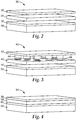
- FIG. 2 illustrates a prior art electrode 30 for a ChLC display.
- a substrate 38 provides support for the device.
- the prior art electrode includes two layers of transparent conductive oxide (TCO) layers 32 and 36 separated by a continuous layer of dielectric polymer 34.
- TCO transparent conductive oxide
- Interfacial reflections 24 and 28, shown in FIG. 1 can occur between the layers, for example at the interfaces of the substrates and electrodes, and such interfacial reflections are undesirable in that they degrade device performance. Reflection losses in other types of reflective and emissive displays can also be detrimental to their performance. Furthermore, for flexible displays and solid state lighting devices, the brittleness of standard TCOs, such as indium tin oxide (ITO), can lead to premature device failure due to cracking and loss of conductivity of the TCO.
- ITO indium tin oxide
- US 5 672 937 A discloses light-transmitting electroconductive plastic film electrodes.
- Flexible translucent electro conductive plastic film electrodes are produced by perforating a normally nonconductive translucent plastic film, and then applying to both surfaces of the film thin layers of a conductive metal oxide such as indium-tin oxide.
- the conductive layers communicate through the perforations to form an electroconductive film electrode useful with an electroluminescent layer and a rear electrode to form lights, signs and similar electroluminescent laminates.
- a solid state lighting element as recited in claim 1 is provided.
- the dependent claims define embodiments.
- a conducting film or electrode includes a substrate and two transparent or semitransparent conductive layers separated by a transparent or semitransparent intervening layer.
- the intervening layer which helps reduce unwanted interfacial reflections occurring in a device incorporating this electrode, includes electrically conductive pathways between the two conductive layers.
- the intervening layer also improves the durability of the conductive layers under conditions of flexing and bending. Use of the intervening layer and the conductive pathways between the conductive layers allows for thinner individual conductive layers. The thinner individual conductive layers are more flexible than a single conductive layer of the same combined conductive layer thickness. Flexing a single thick conductive layer would cause cracking under conditions where the two thinner conductive layers would survive intact.
- the conductive pathways between the two conductive layers also provide redundant electrical pathways such that cracking in one conductive layer will not lead to overall loss of conductivity. In a single thick conductive layer, cracking can lead to open circuits and premature device failure,
- the intervening layers may be chosen to optimize the overall flexibility of the conducting film.
- Embodiments of the present invention relate to a solid state lighting element comprising device substrate electrodes with improved electrical and optical properties.
- the electrodes can be used in any display where, for example, reflections resulting between layers are detrimental to device performance.
- the electrodes can also be used with a variety of types of display materials such as ChLC material or electrochromic material.
- display material refers to any type of material activated by an electrode in a display device.
- Other display devices that can incorporate the electrodes include liquid crystal display devices, electrophoretic, inorganic electroluminescent, polymer dispersed liquid crystal, and organic light emitting diode (OLED) devices.
- the electrodes can also be used in non-display devices such as, for example, passive windows, smart window, solar cells, solid state lighting, and electro-optic devices.
- the present description also mentions a conducting film not used as a display device electrode.
- a conducting film can be used in film applications where the conductivity provides for infrared reflection. Examples of such film applications include the following: window; lighting; architectural; automotive; appliance; and scientific instrument.
- the conducting films can be used in lighting and projectors where visible light is transmitted and infrared heat is reflected by the film.
- the electrode or conducting film includes two or more conductive layers having a particular refractive index with intervening conductive or insulating layers having a different refractive index and having electrically conductive pathways.
- the conductive layers and intervening layers are each transparent or semitransparent.
- the thicknesses of the individual layers and the optical indexes of refraction of the individual layers within the electrode stack are tuned to minimize unwanted Fresnel reflections when these substrates are incorporated within a ChLC display.
- the conductive layers may be symmetric, meaning they have the same thickness. Alternatively, the conductive layers can have different thicknesses.
- This electrode construction significantly improves the black level, color saturation, and hence the contrast of the display.
- the intervening layers permit electrical contact between the conductive layers of the electrode.
- the electrical conductivity of the multilayer electrode is higher than that of the individual conductive layers within the stack. Since the size of the display may be limited by the sheet resistance of the electrodes, the multilayer electrode enables the fabrication of larger display panels. Displays fabricated using the multilayer electrodes exhibit significantly improved electrical and optical performance compared with devices having single layer electrodes.
- a ChLC display does not require polarizers or color filters, resulting in a simpler device construction at a potentially lower cost.
- the red-green-blue (RGB) subpixels are arranged side by side. As a result, only one third of the viewing area is occupied by each of the individual RGB primaries.
- each ChLC RGB subpixel reflects a single primary color while transmitting the other two.
- Each subpixel in a ChLC display includes the ChLC material sandwiched between two conductive substrates.
- the subpixels may be bonded together using an optical adhesive.
- the conductor may be coated and patterned on both sides of each substrate, eliminating the optical adhesive layers.
- Red and yellow color filters may be included to improve color saturation and minimize color shifts with viewing angle.
- the observed color of each stacked pixel is determined by the sum of the reflections from each subpixel. The entire viewing area is utilized by the RGB primaries resulting in significantly improved brightness.
- the light reflected by a pixel In its on (reflective) state, the light reflected by a pixel includes the ChLC planar reflection and unwanted Fresnel reflections at each interface due to refractive index mismatches, represented by reflections 24 and 28 (see FIG. 1 ). Fresnel reflections are typically broadband and hence degrade the color saturation of the display. In its off state, the light reflected by a pixel includes scattering from the semi-transparent focal-conic state and the interfacial Fresnel reflections. These reflections degrade the black level of the display and hence the contrast ratio.
- the highest index step thus occurs at the interfaces between the high index indium tin oxide (ITO) transparent electrode and the polyethylene terephthalate (PET) substrate or the ChLC.
- Device 10 includes two ITO/PET and two ITO/ChLC interfaces. Depending on the illumination and viewing geometry, broadband Fresnel reflections from these interfaces can exceed the reflectivity of the ChLC, significantly degrading display performance.
- the intervening layer in the electrode design is a transparent or semitransparent layer having electrically conductive pathways that enable electrical contact between the two conductive layers.
- the pathways may form naturally by controlling the thickness and deposition conditions of the intervening layer.
- the chemical and physical properties of the first conductive layer nearest the substrate may also be adjusted to enable formation of these pathways by changing the wetting properties of the intervening layer such that the intervening layer is discontinuous to allow electrical contact between the adjacent layers.
- the pathways could be created using techniques such as laser ablation, ion bombardment or wet/dry etching.
- the intervening layer may be deposited using vapor deposition techniques such as sputtering, e-beam, and thermal evaporation.
- the intervening layer can include polymers, including copolymers, such as polyacrylates, polymethacrylates, polyolefins, polyepoxides, polyethers, and the like, and inorganic materials such as metal oxides, nitrides, carbides, and mixtures thereof.
- Preferred non conductive intervening layers include polyacrylates and silicon oxides.
- the intervening layer may also be formed using solution coating. An ultrabarrier film process, in which a monomer is evaporated onto the substrate and cured in-situ, may also be used.
- Ultrabarrier films include multilayer film made, for example, by vacuum deposition of two inorganic dielectric materials sequentially in a multitude of layers on a glass or other suitable substrate, or alternating layers of inorganic materials and organic polymers, as described in U.S. Pat. Nos. 5,440,446 ; 5,877,895 ; and 6,010,751 .
- FIG. 3 An exemplary multilayer device electrode 40 is shown in FIG. 3 .
- This electrode includes two high index conductive layers 42 and 50 of TCO or semitransparent conductive oxide separated by a lower index transparent or semitransparent layer 46 having electrically conductive pathways comprising conductive links 44 extending through apertures 48 in transparent layer 46 to connect the electrodes 42 and 50.
- a substrate 52 provides support for the device. The layers are drawn apart to illustrate the concept.
- the intervening layer is a transparent or semitransparent conductor with a lower refractive index than the conductive layers on either side, as shown in multilayer device electrode 54 of FIG. 4 .
- the intervening conductive layer 58 may provide continuous electrically conductive pathways between the two adjacent conductive layers 56 and 60 of TCO or semitransparent conductive oxide.
- a substrate 62 provides support for the display.
- the intervening layer 58 may comprise a solution coated or electro-deposited conductive polymer. It can also be a vapor deposited transparent conductor.
- Conducting polymers include the following exemplary materials: polyaniline; polypyrrole; polythiophene; and PEDOT/PSS (poly(3,4-ethylenedioxythiophene)/polystyrenesulfonic acid).
- the combined thickness of the conductive layers is constrained by the sheet resistance requirements while the thicknesses of the individual layers are optimized for the desired optical properties.
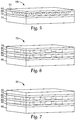
- a solid state lighting element comprises an intervening layer which comprises conductive particles dispersed in a binder, as shown in multilayer device electrode 64 of FIG. 5 .
- the conductive particles 70 in binder 68 provide conductive pathways between the conductive layers 66 and 72 of TCO or semitransparent conductive oxide.
- a substrate 74 provides support for the device.
- the binder can be conductive or insulating.
- the conductive particles can be organic, inorganic, or metallic. Conductive particles also include metal coated particles.
- the refractive index of the intervening layer can be adjusted by varying the volume fractions of the binder and conductive particles.
- the matrix and embedded conducting nanoparticles for the multilayer electrodes can include the following.
- the matrix can include any transparent or semitransparent (conductive or insulating) polymer (for example, acrylates, methacrylates, or the conducting polymers listed above), or a transparent or semitransparent inorganic material either conductive (such as the TCOs listed above) or insulating (SiO 2 , silicon nitride (Si x N y ), Zinc Oxide (Z n O), aluminum oxide (Al 2 O 3 ), or magnesium fluoride (MgF 2 )).
- the conducting nanoparticles can include conducting polymers such as those listed above, metals (for example, silver, gold, nickel, chrome), or metal coated particles. If the matrix is conductive then the nanoparticles can be insulating, in particular they can be nanoparticles of the insulating materials listed above (for example, SiO 2 , silicon nitride, zinc oxide, or other insulating materials.)
- Substrates for devices using the multilayer electrodes can include any type of substrate material for use in making a display or electronic device.
- the substrate can be rigid, for example by using glass or other materials.
- the substrate can also be curved or flexible, for example by using plastics or other materials.
- Substrates can be made using the following exemplary materials: glass; polyethylene terephthalate (PET); polyethylene napthalate (PEN); polycarbonate (PC); polyetheretherketone (PEEK); polyethersulphone (PES); polyarylate (PAR); polyimide (PI); poly(methyl methacrylate) (PMMA); polycyclic olefin (PCO); cellulose triacetate (TAC); and polyurethane (PU).
- CTFE/VDF chlorotrifluoroethylene-vinylidene fluoride copolymer
- ECTFE ethylene-chlorotrifluoroethylene copolymer
- ETFE ethylene-tetrafluoroethylene copolymer
- FEP fluorinated ethylene-propylene copolymer
- PCTFE polychlorotrifluoroethylene
- PFA perfluoroalkyl-tetrafluoroethylene copolymer
- PTFE polytetrafluoroethyloene
- PVDF polyvinylidene fluoride
- PVDF polyvinyl fluoride
- PVDF polyvinyl fluoride
- TFE/HFP tetrafluoroethylene-hexafluoropropylene-vinylidene fluoride terpolymer
- TFE tetrafluoroethylene-hexafluoropropylene-vinylidene fluoride terpolymer
- PCTFE polych
- barrier film examples include barrier film and ultrabarrier films.
- An example of a barrier film is described in U.S. Pat. No. 7,468,211 .
- Ultrabarrier film include multilayer film made, for example, by vacuum deposition of two inorganic dielectric materials sequentially in a multitude of layers on a glass or other suitable substrate, or alternating layers of inorganic materials and organic polymers, as described in U.S. Pat. Nos. 5,440,446 ; 5,877,895 ; and 6,010,751 .
- TCOs for the multilayer electrodes include the following exemplary materials: ITO; tin oxides; cadmium oxides (CdSn 2 O 4 , CdGa 2 O 4 , CdIn 2 O 4 , CdSb 2 O 6 , CdGeO 4 ); indium oxides (In 2 O 3 , Ga, GaInO 3 (Sn, Ge), (GaIn) 2 O 3 ); zinc oxides (ZnO(Al), ZnO(Ga), ZnSnO 3 , Zn 2 SnO 4 , Zn 2 In 2 O 5 , Zn 3 In 2 O 6 ); and magnesium oxides (Mgln 2 O 4 , MgIn 2 O 4 --Zn 2 In 2 O 5 ).
- Device electrodes 76 and 90 shown in FIGS. 6 and 7 include the following layers functioning as a single electrode: multiple transparent or semitransparent conductive layers 78, 82, and 86; intervening transparent or semitransparent layers 80 and 84 between the conductive layers; and a substrate 88. Additional layers of conductive layers and intervening layers can be added as well such that the electrode has any number of layers optimized or tuned for a particular device.
- the layer in contact with the display medium when the electrode is used with a display device, may be insulating or conductive depending on the switching mechanism (for example, current or field driven), such as conductive layer 78 shown in FIG. 6 or an insulating layer 92 shown in FIG. 7 .
- the multilayer electrode can be "tuned" to different optical properties for desired end uses.
- the materials for the intervening layer, and the thicknesses of the layers can be varied for a desired use or property, such as for matching with a multilayer barrier substrate or an OLED optical cavity to enhance light outcoupling.
- the electrodes for each color can be designed or tuned for a particular wavelength range in order to minimize interfacial reflections.
- Table 1 includes thicknesses in nanometers (nm) of an optimized electrode construction for individual colors (RGB ChLC material layers) in a ChLC display device.
- Table 1 Electrode Conductive Layer (ITO) Intervening Layer Conductive Layer (ITO) blue layer 20 42.8 20 green layer 20 46.88 20 red layer 20 56.11 20
- the multilayer electrodes can be used with other display devices such as electrophoretic devices (including use of Bridgestone's powder), polymer dispersed liquid crystal (PDLC) devices, and inorganic electroluminescence (IEL) displays and lighting devices.
- electrophoretic devices including use of Bridgestone's powder
- PDLC polymer dispersed liquid crystal
- IEL inorganic electroluminescence
- Examples of electrophoretic, PDLC, and IEL devices are described in, respectively, U.S. Pat. Nos. 7,365,900 ; 5,629,783 , and 7,538,483 .
- Bridgestone's powder is described in the publication entitled “Quick Response - Liquid Powder Display (QR-LPD)" from Bridgestone Corporation and is also described in U.S. Pat. No. 7,495,820 .
- the multilayer electrodes can also be used with OLED display and lighting devices.
- OLEDs refers to electroluminescent devices that include an organic emissive material.
- the emissive material can include, for example, a small molecule (SM) emitter, a SM doped polymer (also referred to as a molecularly doped polymer or MDP), a light emitting polymer (LEP), a doped LEP, a blended LEP, or any combination of these materials.
- SM small molecule
- MDP molecularly doped polymer
- LEP light emitting polymer
- This emissive material can be provided alone or in combination with any other organic or inorganic materials, including, for example, binders, color converting materials, scattering materials, and electrolytes that are functional or non-functional in the OLED device.
- LECs light emitting electrochemical cells
- LECs are a class of OLEDs with manufacturing advantages as described in U.S. Pat. No. 7,115,216 .
- the organic emissive materials and additional materials, such as charge injection and transport materials, are typically sandwiched as single or multiple layers between two planar electrodes, one of which is typically transparent, to create diffuse light sources or pixilated displays.
- R. H. Friend, et al. (“Electroluminescence in Conjugated Polymers” Nature, 397, 1999, 121 ) describes one mechanism of electroluminescence of such material.
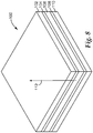
- FIG. 8 is a perspective diagram illustrating a light emitting device 100 according to the invention that incorporates the multilayer electrode of fig. 5 .
- Device 100 includes a stack having the following layers in the configuration as shown: a substrate 102; an electrode 104; a light emitting material 106; an electrode 108; and a substrate 110.
- electrodes 104 and 106 can be implemented with the multilayer electrode of fig. 5 described above.
- Light emitting material 106 when activated emits light as represented by arrow 112, and the light emitting can include OLED or IEL material, or other types of light emitting material for display or solid state lighting devices.
- Device 100 can also have additional layers, such as insulating layers between the electrodes and the light emitting layer for an IEL device.
- FIG. 9 is a perspective diagram of a solar cell 120 that can incorporate the multilayer electrodes.
- Solar cell 120 includes a stack having the following layers in the configuration as shown: a substrate 122; an electrode 124; an active material 126; an electrode 128; and a substrate 130.
- electrodes 124 and 126 can be implemented with the multilayer electrode described above.
- Active material 126 absorbs light as represented by arrow 132 for activating the solar cell in order to convert light energy to electrical energy.
- Solar cells include photovoltaic cells, especially organic photovoltaic (OPV) solar cells. An example of an OPV solar cell is described in U.S. Pat. No., 5,350,459 .
- a TCO electrode, as part of the multilayer electrode, on the side of the solar cell receiving the light can reduce reflectivity losses and thus improve the device efficiency of the solar cell.
- the solar cell can also include barrier films to protect the cell, and particularly the active material, from the environment.
- the intervening layer consisted of an acrylate polymer deposited using the ultrabarrier process identified above, and the two conductive layers consisted of sputter deposited ITO.
- Three layer electrodes with different intervening layer and ITO layer thicknesses were fabricated on a roll of 0.005 inch thick PET as identified in Table 2.
- Table 2 Design ITO 1 fpm Polymer fpm ITO 2 fpm 1 3.8 68 3.8 2 4.3 68 4.3 3 4.8 68 4.8 4 4.8 66 4.8 5 3.8 66 3.8 6 3.8 64 3.8 7 4.3 64 4.3 8 4.8 64 4.8
- the individual layer thicknesses were determined by the speed of the film in feet per minute (fpm) across the ITO and ultrabarrier film deposition sources. Faster speeds yield thinner layers.
- the sheet resistance of these samples was measured using a noncontact probe (Delcom) that measures the combined conductivity of both ITO layers and a surface contact 4-probe instrument that measures the conductivity of the top, exposed surface. Both measurement techniques yielded sheet resistance values that are identical within the measurement error indicating that the intervening layer permits electrical contact between the two adjacent ITO layers.
- the color gamut of the device with the index matched electrodes was three times larger than that of the device with the non-index matched electrodes.
- the stronger interfacial reflections also degraded the black level of devices with non-index matched electrodes relative to those with index matched electrodes.
- the contrast ratio defined as the ratio of the brightness (CIE Y) of the white to black states, was much higher for devices with index matched electrodes.
- Devices were also fabricated from three-layer electrode substrates in which the intervening layer consisted of SiO 2 , an inorganic material instead of the ultrabarrier film layer.
- the three-layer electrode consisted of ITO(20 nm)/SiO 2 (42 nm)/ITO(20 nm), which were sputtered onto 5 mil PET (Dupont Teijin, ST-504). These substrates also exhibited improved electrical and optical properties when incorporated into ChLC, RGB devices. Both the color saturation (Gamut) and contrast were significantly higher for the device with the index matched, three-layer electrode. The color gamut was over four times larger and the contrast over five times higher with the three-layer index matched electrode.
- the three layer electrode design also enables low sheet resistance in conjunction with good optical performance.
- Each intervening low index layer permits electrical contact between the adjacent transparent conductive layers.
- the conductivity of the multilayer electrode is determined by the combined thickness of all the conductive layers.
- a display was fabricated from substrates with the three layer electrode. The lower sheet resistance of this substrate (approximately 100 ohms/sq) compared to those using a single layer electrode enabled excellent display uniformity with no fading in the pattern across the display. Both the color saturation and display uniformity were observed to be very good.
- a multilayer ITO/polymer/ITO stack was fabricated on PET film in the same process as used for Example 1.
- a laser ablation technique was used to define electrodes for OLED fabrication.
- PET film with ITO/polymer/ITO multilayer stack was pre-baked at 80°C overnight in nitrogen atmosphere in order to remove moisture from the film.
- the film was treated to a standard oxygen plasma procedure to remove organic residues off the ITO surface and tune the ITO surface characteristics for optimal performance in OLEDs.
- the OLEDs were fabricated by standard thermal deposition in a vacuum system at base pressure of ca. 10 -6 torr. The following OLED construction was deposited: HIL(300nm)/HTL(40nm)/EML(30nm,6% dopant)/ETL(20nm)/LiF(1nm)/Al(200nm).
- the OLEDs were encapsulated with 3M encapsulation barrier film employing SAES getter as a desiccant and oxygen scavenger in between the encapsulation film and the OLED cathode.
- the barrier film was 5 mil PET prepared as described in U.S. Pat. No. 7,018,713 .
- the desiccant was CaO from SAES Getters, Colorado Springs, Colorado, USA. Both reference OLEDs on standard PET/ITO (100nm) substrates and OLEDs on PET/ITO/polymer/ITO multilayer stack were fabricated according to the above-described routine.
- Luminance-voltage-current (LIV) characteristics and electroluminescence spectra of the fabricated OLEDs were recorded using a Keithley 2400 source meter as a current source/voltage detector and PhotoResearch PR650 camera as a luminance and spectral detector.
- the devices with the multilayer stack ITO showed very similar LIV behavior as the reference ones indicating that the multilayer stacked ITO has equivalent electrical performance to the reference ITO, and no additional optical losses are induced by the multilayer stack ITO.
- Luminance and electroluminescence spectra were also recorded also at various angles for both reference and multilayer stack ITO devices, and it was found they both ITO exhibited very similar angular performance with slightly reduced optical cavity effects with the multilayer ITO stack.
Landscapes
- Physics & Mathematics (AREA)
- Nonlinear Science (AREA)
- Optics & Photonics (AREA)
- Chemical & Material Sciences (AREA)
- General Physics & Mathematics (AREA)
- Mathematical Physics (AREA)
- Crystallography & Structural Chemistry (AREA)
- Electromagnetism (AREA)
- Dispersion Chemistry (AREA)
- Electroluminescent Light Sources (AREA)
- Devices For Indicating Variable Information By Combining Individual Elements (AREA)
- Photovoltaic Devices (AREA)
- Liquid Crystal (AREA)
- Planar Illumination Modules (AREA)
- Health & Medical Sciences (AREA)
- Life Sciences & Earth Sciences (AREA)
- Chemical Kinetics & Catalysis (AREA)
- Electrochemistry (AREA)
- Molecular Biology (AREA)
- Laminated Bodies (AREA)
- Non-Insulated Conductors (AREA)
Description
- A cholesteric liquid crystal (ChLC) material consists of a nematic liquid crystal and a chiral additive blended together to spontaneously form a helical structure with a well defined pitch. This pitch determines the wavelength of light reflected by the material and hence the color of it. The color can also be adjusted by varying the ratio of the nematic liquid crystal and chiral components. A pixel in a ChLC display can be switched between its planar reflective (colored) state and its semi-transparent focal conic state by application of an appropriate drive scheme.
-
FIG. 1 illustrates a singlecolor ChLC display 10, including a stack having the following layers in the configuration as shown: asubstrate 12; anelectrode 14; aChLC material 16; anelectrode 18; asubstrate 20; and ablack absorber 22. Areflection 26 fromChLC material 16 results in a displayed color. A full color ChLC display can be constructed by stacking a set of RGB panels with the individual RGB subpixels overlapped on top of each other and reflecting different regions of the spectrum. The back of the display panel is coated with broadband absorber 22 that absorbs the light not reflected by the preceding layers. Black absorbers include the following exemplary materials: KRYLON matte or glossy black acrylic enamel spray paint. -
FIG. 2 illustrates aprior art electrode 30 for a ChLC display. Asubstrate 38 provides support for the device. The prior art electrode includes two layers of transparent conductive oxide (TCO)layers dielectric polymer 34. -
Interfacial reflections FIG. 1 , can occur between the layers, for example at the interfaces of the substrates and electrodes, and such interfacial reflections are undesirable in that they degrade device performance. Reflection losses in other types of reflective and emissive displays can also be detrimental to their performance. Furthermore, for flexible displays and solid state lighting devices, the brittleness of standard TCOs, such as indium tin oxide (ITO), can lead to premature device failure due to cracking and loss of conductivity of the TCO. -
US 5 672 937 A discloses light-transmitting electroconductive plastic film electrodes. Flexible translucent electro conductive plastic film electrodes are produced by perforating a normally nonconductive translucent plastic film, and then applying to both surfaces of the film thin layers of a conductive metal oxide such as indium-tin oxide. The conductive layers communicate through the perforations to form an electroconductive film electrode useful with an electroluminescent layer and a rear electrode to form lights, signs and similar electroluminescent laminates. - A solid state lighting element as recited in claim 1 is provided. The dependent claims define embodiments.
- A conducting film or electrode, consistent with the present invention, includes a substrate and two transparent or semitransparent conductive layers separated by a transparent or semitransparent intervening layer. The intervening layer, which helps reduce unwanted interfacial reflections occurring in a device incorporating this electrode, includes electrically conductive pathways between the two conductive layers. The intervening layer also improves the durability of the conductive layers under conditions of flexing and bending. Use of the intervening layer and the conductive pathways between the conductive layers allows for thinner individual conductive layers. The thinner individual conductive layers are more flexible than a single conductive layer of the same combined conductive layer thickness. Flexing a single thick conductive layer would cause cracking under conditions where the two thinner conductive layers would survive intact. The conductive pathways between the two conductive layers also provide redundant electrical pathways such that cracking in one conductive layer will not lead to overall loss of conductivity. In a single thick conductive layer, cracking can lead to open circuits and premature device failure, The intervening layers may be chosen to optimize the overall flexibility of the conducting film.
- The accompanying drawings are incorporated in and constitute a part of this specification and, together with the description, explain the advantages and principles of the invention. In the drawings,
-
FIG. 1 is a perspective diagram of a single color ChLC display construction; -
FIG. 2 is a diagram of a prior art electrode for a ChLC display; -
FIG. 3 is a diagram of a device electrode having an intervening layer with conductive paths; -
FIG. 4 is a diagram of a device electrode having an intervening conductive layer; -
FIG. 5 is a diagram of a device electrode having an intervening layer with conductive particles dispersed in a binder; -
FIG. 6 is a diagram of a device electrode having multiple intervening layers and a conductive layer to be in contact with a display medium; -
FIG. 7 is a diagram of a device electrode having multiple intervening layers and an insulating layer to be in contact with a display medium; -
FIG. 8 is a perspective diagram illustrating a light emitting device; and -
FIG. 9 is a perspective diagram illustrating a solar cell. - Embodiments of the present invention relate to a solid state lighting element comprising device substrate electrodes with improved electrical and optical properties. The electrodes can be used in any display where, for example, reflections resulting between layers are detrimental to device performance. The electrodes can also be used with a variety of types of display materials such as ChLC material or electrochromic material. The term display material refers to any type of material activated by an electrode in a display device. Other display devices that can incorporate the electrodes include liquid crystal display devices, electrophoretic, inorganic electroluminescent, polymer dispersed liquid crystal, and organic light emitting diode (OLED) devices. The electrodes can also be used in non-display devices such as, for example, passive windows, smart window, solar cells, solid state lighting, and electro-optic devices. The present description also mentions a conducting film not used as a display device electrode. Such a conducting film can be used in film applications where the conductivity provides for infrared reflection. Examples of such film applications include the following: window; lighting; architectural; automotive; appliance; and scientific instrument. The conducting films can be used in lighting and projectors where visible light is transmitted and infrared heat is reflected by the film.
- The electrode or conducting film includes two or more conductive layers having a particular refractive index with intervening conductive or insulating layers having a different refractive index and having electrically conductive pathways. The conductive layers and intervening layers are each transparent or semitransparent. The thicknesses of the individual layers and the optical indexes of refraction of the individual layers within the electrode stack are tuned to minimize unwanted Fresnel reflections when these substrates are incorporated within a ChLC display. The conductive layers may be symmetric, meaning they have the same thickness. Alternatively, the conductive layers can have different thicknesses.
- This electrode construction significantly improves the black level, color saturation, and hence the contrast of the display. In addition, the intervening layers permit electrical contact between the conductive layers of the electrode. As a result, the electrical conductivity of the multilayer electrode is higher than that of the individual conductive layers within the stack. Since the size of the display may be limited by the sheet resistance of the electrodes, the multilayer electrode enables the fabrication of larger display panels. Displays fabricated using the multilayer electrodes exhibit significantly improved electrical and optical performance compared with devices having single layer electrodes.
- Unlike a conventional nematic liquid crystal (NLC) based display, a ChLC display does not require polarizers or color filters, resulting in a simpler device construction at a potentially lower cost. In a full color NLC display, the red-green-blue (RGB) subpixels are arranged side by side. As a result, only one third of the viewing area is occupied by each of the individual RGB primaries. On the other hand, each ChLC RGB subpixel reflects a single primary color while transmitting the other two.
- Each subpixel in a ChLC display includes the ChLC material sandwiched between two conductive substrates. The subpixels may be bonded together using an optical adhesive. Alternatively, the conductor may be coated and patterned on both sides of each substrate, eliminating the optical adhesive layers. Red and yellow color filters may be included to improve color saturation and minimize color shifts with viewing angle. The observed color of each stacked pixel is determined by the sum of the reflections from each subpixel. The entire viewing area is utilized by the RGB primaries resulting in significantly improved brightness.
- In its on (reflective) state, the light reflected by a pixel includes the ChLC planar reflection and unwanted Fresnel reflections at each interface due to refractive index mismatches, represented by
reflections 24 and 28 (seeFIG. 1 ). Fresnel reflections are typically broadband and hence degrade the color saturation of the display. In its off state, the light reflected by a pixel includes scattering from the semi-transparent focal-conic state and the interfacial Fresnel reflections. These reflections degrade the black level of the display and hence the contrast ratio. - The magnitude of the Fresnel reflection depends on the ratio of refractive indices at the interface. At normal incidence it is determined by the following equation:


device 10 shown inFIG. 1 are the following: n = 2.0 for the electrodes; n = 1.65 for the substrate; and n = 1.55 for the ChLC material. Indevice 10, the highest index step thus occurs at the interfaces between the high index indium tin oxide (ITO) transparent electrode and the polyethylene terephthalate (PET) substrate or the ChLC.Device 10 includes two ITO/PET and two ITO/ChLC interfaces. Depending on the illumination and viewing geometry, broadband Fresnel reflections from these interfaces can exceed the reflectivity of the ChLC, significantly degrading display performance. - In comparison, the electrode design which is here described yields both good optical and electrical performance. The intervening layer in the electrode design is a transparent or semitransparent layer having electrically conductive pathways that enable electrical contact between the two conductive layers. The pathways may form naturally by controlling the thickness and deposition conditions of the intervening layer. The chemical and physical properties of the first conductive layer nearest the substrate may also be adjusted to enable formation of these pathways by changing the wetting properties of the intervening layer such that the intervening layer is discontinuous to allow electrical contact between the adjacent layers. Alternatively, the pathways could be created using techniques such as laser ablation, ion bombardment or wet/dry etching.
- The intervening layer may be deposited using vapor deposition techniques such as sputtering, e-beam, and thermal evaporation. The intervening layer can include polymers, including copolymers, such as polyacrylates, polymethacrylates, polyolefins, polyepoxides, polyethers, and the like, and inorganic materials such as metal oxides, nitrides, carbides, and mixtures thereof. Preferred non conductive intervening layers include polyacrylates and silicon oxides. The intervening layer may also be formed using solution coating. An ultrabarrier film process, in which a monomer is evaporated onto the substrate and cured in-situ, may also be used. Ultrabarrier films include multilayer film made, for example, by vacuum deposition of two inorganic dielectric materials sequentially in a multitude of layers on a glass or other suitable substrate, or alternating layers of inorganic materials and organic polymers, as described in
U.S. Pat. Nos. 5,440,446 ;5,877,895 ; and6,010,751 . - An exemplary
multilayer device electrode 40 is shown inFIG. 3 . This electrode includes two high indexconductive layers semitransparent layer 46 having electrically conductive pathways comprisingconductive links 44 extending throughapertures 48 intransparent layer 46 to connect theelectrodes substrate 52 provides support for the device. The layers are drawn apart to illustrate the concept. - In another exemplary multilayer device electrode, the intervening layer is a transparent or semitransparent conductor with a lower refractive index than the conductive layers on either side, as shown in
multilayer device electrode 54 ofFIG. 4 . Inelectrode 54, the interveningconductive layer 58 may provide continuous electrically conductive pathways between the two adjacentconductive layers substrate 62 provides support for the display. The interveninglayer 58 may comprise a solution coated or electro-deposited conductive polymer. It can also be a vapor deposited transparent conductor. Conducting polymers include the following exemplary materials: polyaniline; polypyrrole; polythiophene; and PEDOT/PSS (poly(3,4-ethylenedioxythiophene)/polystyrenesulfonic acid). The combined thickness of the conductive layers is constrained by the sheet resistance requirements while the thicknesses of the individual layers are optimized for the desired optical properties. - In an embodiment, a solid state lighting element comprises an intervening layer which comprises conductive particles dispersed in a binder, as shown in
multilayer device electrode 64 ofFIG. 5 . Theconductive particles 70 in binder 68 provide conductive pathways between theconductive layers 66 and 72 of TCO or semitransparent conductive oxide. A substrate 74 provides support for the device. The binder can be conductive or insulating. The conductive particles can be organic, inorganic, or metallic. Conductive particles also include metal coated particles. The refractive index of the intervening layer can be adjusted by varying the volume fractions of the binder and conductive particles. - The matrix and embedded conducting nanoparticles for the multilayer electrodes can include the following. The matrix can include any transparent or semitransparent (conductive or insulating) polymer (for example, acrylates, methacrylates, or the conducting polymers listed above), or a transparent or semitransparent inorganic material either conductive (such as the TCOs listed above) or insulating (SiO2, silicon nitride (SixNy), Zinc Oxide (ZnO), aluminum oxide (Al2O3), or magnesium fluoride (MgF2)). The conducting nanoparticles can include conducting polymers such as those listed above, metals (for example, silver, gold, nickel, chrome), or metal coated particles. If the matrix is conductive then the nanoparticles can be insulating, in particular they can be nanoparticles of the insulating materials listed above (for example, SiO2, silicon nitride, zinc oxide, or other insulating materials.)
- Substrates for devices using the multilayer electrodes can include any type of substrate material for use in making a display or electronic device. The substrate can be rigid, for example by using glass or other materials. The substrate can also be curved or flexible, for example by using plastics or other materials. Substrates can be made using the following exemplary materials: glass; polyethylene terephthalate (PET); polyethylene napthalate (PEN); polycarbonate (PC); polyetheretherketone (PEEK); polyethersulphone (PES); polyarylate (PAR); polyimide (PI); poly(methyl methacrylate) (PMMA); polycyclic olefin (PCO); cellulose triacetate (TAC); and polyurethane (PU).
- Other suitable materials for the substrate include chlorotrifluoroethylene-vinylidene fluoride copolymer (CTFE/VDF), ethylene-chlorotrifluoroethylene copolymer (ECTFE), ethylene-tetrafluoroethylene copolymer (ETFE), fluorinated ethylene-propylene copolymer (FEP), polychlorotrifluoroethylene (PCTFE), perfluoroalkyl-tetrafluoroethylene copolymer (PFA), polytetrafluoroethyloene (PTFE), polyvinylidene fluoride (PVDF), polyvinyl fluoride (PVF), tetrafluoroethylene-hexafluoropropylene copolymer (TFE/HFP), tetrafluoroethylene-hexafluoropropylene-vinylidene fluoride terpolymer (THV), polychlorotrifluoroethylene (PCTFE), hexafluoropropylene-vinylidene fluoride copolymer (HFP/VDF), tetrafluoroethylene-propylene copolymer (TFE/P), and tetrafluoroethylene-perfluoromethylether copolymer (TFE/PFMe).
- Other suitable substrates include barrier film and ultrabarrier films. An example of a barrier film is described in
U.S. Pat. No. 7,468,211 . Ultrabarrier film include multilayer film made, for example, by vacuum deposition of two inorganic dielectric materials sequentially in a multitude of layers on a glass or other suitable substrate, or alternating layers of inorganic materials and organic polymers, as described inU.S. Pat. Nos. 5,440,446 ;5,877,895 ; and6,010,751 . - TCOs for the multilayer electrodes include the following exemplary materials: ITO; tin oxides; cadmium oxides (CdSn2O4, CdGa2O4, CdIn2O4, CdSb2O6, CdGeO4); indium oxides (In2O3, Ga, GaInO3 (Sn, Ge), (GaIn)2O3); zinc oxides (ZnO(Al), ZnO(Ga), ZnSnO3, Zn2SnO4, Zn2In2O5, Zn3In2O6); and magnesium oxides (Mgln2O4, MgIn2O4--Zn2In2O5).
- While the device electrodes described above include two transparent or semitransparent conductive layers separated by an intervening layer, additional transparent or semitransparent conductive and intervening layers may be added depending on the desired optical and electrical properties, as shown in
FIGS. 6 and 7 .Device electrodes FIGS. 6 and 7 include the following layers functioning as a single electrode: multiple transparent or semitransparentconductive layers semitransparent layers substrate 88. Additional layers of conductive layers and intervening layers can be added as well such that the electrode has any number of layers optimized or tuned for a particular device. Also, the layer in contact with the display medium, when the electrode is used with a display device, may be insulating or conductive depending on the switching mechanism (for example, current or field driven), such asconductive layer 78 shown inFIG. 6 or an insulatinglayer 92 shown inFIG. 7 . Furthermore, the multilayer electrode can be "tuned" to different optical properties for desired end uses. For example, the materials for the intervening layer, and the thicknesses of the layers, can be varied for a desired use or property, such as for matching with a multilayer barrier substrate or an OLED optical cavity to enhance light outcoupling. - For a three color ChLC display, the electrodes for each color can be designed or tuned for a particular wavelength range in order to minimize interfacial reflections. Table 1 includes thicknesses in nanometers (nm) of an optimized electrode construction for individual colors (RGB ChLC material layers) in a ChLC display device.
Table 1 Electrode Conductive Layer (ITO) Intervening Layer Conductive Layer (ITO) blue layer 20 42.8 20 green layer 20 46.88 20 red layer 20 56.11 20 - The multilayer electrodes can be used with other display devices such as electrophoretic devices (including use of Bridgestone's powder), polymer dispersed liquid crystal (PDLC) devices, and inorganic electroluminescence (IEL) displays and lighting devices. Examples of electrophoretic, PDLC, and IEL devices are described in, respectively,
U.S. Pat. Nos. 7,365,900 ;5,629,783 , and7,538,483 . Bridgestone's powder is described in the publication entitled "Quick Response - Liquid Powder Display (QR-LPD)" from Bridgestone Corporation and is also described inU.S. Pat. No. 7,495,820 . - The multilayer electrodes can also be used with OLED display and lighting devices. OLEDs refers to electroluminescent devices that include an organic emissive material. The emissive material can include, for example, a small molecule (SM) emitter, a SM doped polymer (also referred to as a molecularly doped polymer or MDP), a light emitting polymer (LEP), a doped LEP, a blended LEP, or any combination of these materials. This emissive material can be provided alone or in combination with any other organic or inorganic materials, including, for example, binders, color converting materials, scattering materials, and electrolytes that are functional or non-functional in the OLED device. Addition of electrolyte provides for light emitting electrochemical cells (LECs), such as those described in
U.S. Pat. No. 5,682,043 . LECs are a class of OLEDs with manufacturing advantages as described inU.S. Pat. No. 7,115,216 . The organic emissive materials and additional materials, such as charge injection and transport materials, are typically sandwiched as single or multiple layers between two planar electrodes, one of which is typically transparent, to create diffuse light sources or pixilated displays. R. H. Friend, et al. ("Electroluminescence in Conjugated Polymers" Nature, 397, 1999, 121) describes one mechanism of electroluminescence of such material. -
FIG. 8 is a perspective diagram illustrating alight emitting device 100 according to the invention that incorporates the multilayer electrode offig. 5 .Device 100 includes a stack having the following layers in the configuration as shown: asubstrate 102; anelectrode 104; alight emitting material 106; anelectrode 108; and asubstrate 110. One or both ofelectrodes fig. 5 described above.Light emitting material 106 when activated emits light as represented byarrow 112, and the light emitting can include OLED or IEL material, or other types of light emitting material for display or solid state lighting devices.Device 100 can also have additional layers, such as insulating layers between the electrodes and the light emitting layer for an IEL device. -
FIG. 9 is a perspective diagram of asolar cell 120 that can incorporate the multilayer electrodes.Solar cell 120 includes a stack having the following layers in the configuration as shown: asubstrate 122; anelectrode 124; anactive material 126; anelectrode 128; and asubstrate 130. One or both ofelectrodes Active material 126 absorbs light as represented byarrow 132 for activating the solar cell in order to convert light energy to electrical energy. Solar cells include photovoltaic cells, especially organic photovoltaic (OPV) solar cells. An example of an OPV solar cell is described in U.S. Pat. No.,5,350,459 . A TCO electrode, as part of the multilayer electrode, on the side of the solar cell receiving the light can reduce reflectivity losses and thus improve the device efficiency of the solar cell. The solar cell can also include barrier films to protect the cell, and particularly the active material, from the environment. - Substrates with the three-layer electrode design shown in
FIG. 4 were fabricated. The intervening layer consisted of an acrylate polymer deposited using the ultrabarrier process identified above, and the two conductive layers consisted of sputter deposited ITO. Three layer electrodes with different intervening layer and ITO layer thicknesses were fabricated on a roll of 0.005 inch thick PET as identified in Table 2.Table 2 Design ITO 1 fpm Polymer fpm ITO 2 fpm 1 3.8 68 3.8 2 4.3 68 4.3 3 4.8 68 4.8 4 4.8 66 4.8 5 3.8 66 3.8 6 3.8 64 3.8 7 4.3 64 4.3 8 4.8 64 4.8 - The individual layer thicknesses were determined by the speed of the film in feet per minute (fpm) across the ITO and ultrabarrier film deposition sources. Faster speeds yield thinner layers. The sheet resistance of these samples was measured using a noncontact probe (Delcom) that measures the combined conductivity of both ITO layers and a surface contact 4-probe instrument that measures the conductivity of the top, exposed surface. Both measurement techniques yielded sheet resistance values that are identical within the measurement error indicating that the intervening layer permits electrical contact between the two adjacent ITO layers.
- Full color RGB, ChLC devices fabricated using substrates having index matched three-layer electrodes, and single layer non-index matched electrodes were compared. The broadband, interfacial reflection was much more pronounced with the non-index matched electrode. These reflections degrade the color saturation relative to devices with index matched electrodes.
- The color gamut of the device with the index matched electrodes was three times larger than that of the device with the non-index matched electrodes. The stronger interfacial reflections also degraded the black level of devices with non-index matched electrodes relative to those with index matched electrodes. As a result the contrast ratio, defined as the ratio of the brightness (CIE Y) of the white to black states, was much higher for devices with index matched electrodes.
- Devices were also fabricated from three-layer electrode substrates in which the intervening layer consisted of SiO2, an inorganic material instead of the ultrabarrier film layer. The three-layer electrode consisted of ITO(20 nm)/SiO2(42 nm)/ITO(20 nm), which were sputtered onto 5 mil PET (Dupont Teijin, ST-504). These substrates also exhibited improved electrical and optical properties when incorporated into ChLC, RGB devices. Both the color saturation (Gamut) and contrast were significantly higher for the device with the index matched, three-layer electrode. The color gamut was over four times larger and the contrast over five times higher with the three-layer index matched electrode.
- The three layer electrode design also enables low sheet resistance in conjunction with good optical performance. Each intervening low index layer permits electrical contact between the adjacent transparent conductive layers. As a result the conductivity of the multilayer electrode is determined by the combined thickness of all the conductive layers. A display was fabricated from substrates with the three layer electrode. The lower sheet resistance of this substrate (approximately 100 ohms/sq) compared to those using a single layer electrode enabled excellent display uniformity with no fading in the pattern across the display. Both the color saturation and display uniformity were observed to be very good.
- A multilayer ITO/polymer/ITO stack was fabricated on PET film in the same process as used for Example 1. A laser ablation technique was used to define electrodes for OLED fabrication. Prior to OLED fabrication, PET film with ITO/polymer/ITO multilayer stack was pre-baked at 80°C overnight in nitrogen atmosphere in order to remove moisture from the film. Immediately before OLED fabrication, the film was treated to a standard oxygen plasma procedure to remove organic residues off the ITO surface and tune the ITO surface characteristics for optimal performance in OLEDs. The OLEDs were fabricated by standard thermal deposition in a vacuum system at base pressure of ca. 10-6 torr. The following OLED construction was deposited: HIL(300nm)/HTL(40nm)/EML(30nm,6% dopant)/ETL(20nm)/LiF(1nm)/Al(200nm).
- After completion, the OLEDs were encapsulated with 3M encapsulation barrier film employing SAES getter as a desiccant and oxygen scavenger in between the encapsulation film and the OLED cathode. The barrier film was 5 mil PET prepared as described in
U.S. Pat. No. 7,018,713 . The desiccant was CaO from SAES Getters, Colorado Springs, Colorado, USA. Both reference OLEDs on standard PET/ITO (100nm) substrates and OLEDs on PET/ITO/polymer/ITO multilayer stack were fabricated according to the above-described routine. - Luminance-voltage-current (LIV) characteristics and electroluminescence spectra of the fabricated OLEDs were recorded using a Keithley 2400 source meter as a current source/voltage detector and PhotoResearch PR650 camera as a luminance and spectral detector. The devices with the multilayer stack ITO showed very similar LIV behavior as the reference ones indicating that the multilayer stacked ITO has equivalent electrical performance to the reference ITO, and no additional optical losses are induced by the multilayer stack ITO. Luminance and electroluminescence spectra were also recorded also at various angles for both reference and multilayer stack ITO devices, and it was found they both ITO exhibited very similar angular performance with slightly reduced optical cavity effects with the multilayer ITO stack.
Claims (3)
- A solid state lighting element (100), comprising layers arranged in the following order:a first substrate (102);a first electrode (104);a light emitting material (106);a second electrode (108); anda second substrate (110),wherein at least one of the first and second electrodes (104, 108) comprises:a first transparent or semitransparent conductive layer (66; 78);a second transparent or semitransparent conductive layer (72; 82); anda transparent or semitransparent intervening layer (68; 80) located between the first and second conductive layers,wherein the intervening layer (68, 70; 80) includes electrically conductive pathways between the first and second conductive layers, wherein the intervening layer (68, 70; 80) comprises conductive particles (70) dispersed in a binder (68), the conductive particles (70) providing the electrically conductive pathways.
- The solid state lighting element of claim 1, wherein the light emitting material (106) comprises an organic light emitting diode, OLED, material.
- The solid state lighting element of claim 1, wherein the light emitting material (106) comprises an inorganic electroluminescent, IEL, material.
Applications Claiming Priority (2)
| Application Number | Priority Date | Filing Date | Title |
|---|---|---|---|
| US12/540,394 US9581870B2 (en) | 2009-08-13 | 2009-08-13 | Conducting film or electrode with improved optical and electrical performance for display and lighting devices and solar cells |
| PCT/US2010/044831 WO2011019629A2 (en) | 2009-08-13 | 2010-08-09 | Conducting film or electrode with improved optical and electrical performance for display and lighting devices and solar cells |
Publications (3)
| Publication Number | Publication Date |
|---|---|
| EP2465006A2 EP2465006A2 (en) | 2012-06-20 |
| EP2465006A4 EP2465006A4 (en) | 2015-04-22 |
| EP2465006B1 true EP2465006B1 (en) | 2017-11-22 |
Family
ID=43586758
Family Applications (1)
| Application Number | Title | Priority Date | Filing Date |
|---|---|---|---|
| EP10808572.1A Not-in-force EP2465006B1 (en) | 2009-08-13 | 2010-08-09 | Solid state lighting element comprising an electrode with improved optical and electrical performances |
Country Status (7)
| Country | Link |
|---|---|
| US (2) | US9581870B2 (en) |
| EP (1) | EP2465006B1 (en) |
| JP (1) | JP5612686B2 (en) |
| KR (1) | KR101770002B1 (en) |
| CN (1) | CN102576168B (en) |
| TW (1) | TWI503803B (en) |
| WO (1) | WO2011019629A2 (en) |
Families Citing this family (31)
| Publication number | Priority date | Publication date | Assignee | Title |
|---|---|---|---|---|
| US9581870B2 (en) * | 2009-08-13 | 2017-02-28 | 3M Innovative Properties Company | Conducting film or electrode with improved optical and electrical performance for display and lighting devices and solar cells |
| US8730184B2 (en) * | 2009-12-16 | 2014-05-20 | 3M Innovative Properties Company | Touch sensitive device with multilayer electrode having improved optical and electrical performance |
| CN103026525B (en) * | 2010-07-26 | 2016-11-09 | 默克专利有限公司 | Nanocrystals in Devices |
| US8941006B2 (en) | 2011-02-25 | 2015-01-27 | Fina Technology, Inc. | Apparatus and method for extending polyolefin containing photovoltaic panel life span |
| WO2012170415A2 (en) * | 2011-06-09 | 2012-12-13 | 3M Innovative Properties Company | Method of making touch sensitive device with multilayer electrode and underlayer |
| WO2012170399A2 (en) * | 2011-06-09 | 2012-12-13 | 3M Innovative Properties Company | Touch sensitive device with multilayer electrode and underlayer |
| ES2599370T3 (en) * | 2011-06-23 | 2017-02-01 | Big Solar Limited | Method for manufacturing a structure comprising coating steps and corresponding device |
| GB2497958B (en) * | 2011-12-23 | 2018-06-27 | Braghiroli Marco | Photovoltaic sleeve for street lights and the like |
| WO2013169047A1 (en) | 2012-05-09 | 2013-11-14 | 주식회사 엘지화학 | Organic electrochemical device, and method for manufacturing same |
| TWI486832B (en) * | 2012-11-01 | 2015-06-01 | Transtouch Technology Inc | Conductive substrate, touch panel using the same thereof and flat touch display device using the same |
| GB201301683D0 (en) | 2013-01-30 | 2013-03-13 | Big Solar Ltd | Method of creating non-conductive delineations with a selective coating technology on a structured surface |
| WO2015066623A1 (en) * | 2013-11-01 | 2015-05-07 | The Regents Of The University Of Michigan | Decorative dual-function photovoltaic devices generating angle insensitive transmissive or reflective colors |
| US9818976B2 (en) * | 2014-05-13 | 2017-11-14 | Apple Inc. | Encapsulation layers with improved reliability |
| KR102240456B1 (en) * | 2014-07-30 | 2021-04-15 | 에스케이하이닉스 주식회사 | Semiconductor device with optical through via |
| KR20160100006A (en) * | 2015-02-13 | 2016-08-23 | 삼성디스플레이 주식회사 | structure for a display apparatus and display apparatus including the same |
| KR101707737B1 (en) * | 2015-06-04 | 2017-02-16 | 고려대학교 산학협력단 | Electrode structure and method of manufacturing the same |
| US9595448B2 (en) * | 2015-06-29 | 2017-03-14 | Taiwan Semiconductor Manufacturing Co., Ltd. | Method for cleaning plasma processing chamber and substrate |
| EP3133649A1 (en) * | 2015-08-18 | 2017-02-22 | Saint-Gobain Performance Plastics Corporation | Flexible functionalized film |
| JP6680883B2 (en) * | 2015-12-16 | 2020-04-15 | サン−ゴバン グラス フランス | Electrically switchable glazing with surface electrodes having anisotropic conductivity |
| GB2549134B (en) | 2016-04-07 | 2020-02-12 | Power Roll Ltd | Asymmetric groove |
| GB2549133B (en) | 2016-04-07 | 2020-02-19 | Power Roll Ltd | Gap between semiconductors |
| GB2549132A (en) | 2016-04-07 | 2017-10-11 | Big Solar Ltd | Aperture in a semiconductor |
| JP2020502777A (en) * | 2016-09-27 | 2020-01-23 | イヌル ゲーエムベーハー | Non-destructive integration of electronic devices |
| GB201617276D0 (en) | 2016-10-11 | 2016-11-23 | Big Solar Limited | Energy storage |
| GB2565041B (en) * | 2017-06-19 | 2021-12-29 | Liddle Richard | Transparent structure with electrically conductive elements |
| US10886033B2 (en) * | 2017-09-28 | 2021-01-05 | Regents Of The University Of Minnesota | Conductive films |
| CN108957813B (en) * | 2018-08-24 | 2021-11-12 | 南京京东方显示技术有限公司 | Reflective display and manufacturing method thereof |
| CN109275210B (en) * | 2018-10-12 | 2021-02-09 | 重庆墨希科技有限公司 | High-reliability heating film based on graphene and preparation method thereof |
| KR20220108275A (en) * | 2021-01-26 | 2022-08-03 | 삼성디스플레이 주식회사 | Light emitting device and electronic apparatus including the same |
| US12547038B2 (en) | 2021-09-16 | 2026-02-10 | Gentex Corporation | Electro-optic element electrodes |
| CN116386477A (en) * | 2023-05-22 | 2023-07-04 | 深圳御光新材料有限公司 | A high-consistency transparent display light-emitting plate and a method for manufacturing the transparent display |
Family Cites Families (75)
| Publication number | Priority date | Publication date | Assignee | Title |
|---|---|---|---|---|
| JPS58139647U (en) | 1982-03-17 | 1983-09-20 | 株式会社東芝 | Earth leakage breaker display device |
| JP2728248B2 (en) | 1987-07-24 | 1998-03-18 | 富士通株式会社 | Projection type liquid crystal display |
| JPH01261495A (en) | 1988-04-13 | 1989-10-18 | Fujitsu Ltd | Phase transition type liquid crystal material |
| JPH02199790A (en) * | 1989-01-27 | 1990-08-08 | Furukawa Electric Co Ltd:The | Manufacture of electroluminescence display element |
| JPH05308146A (en) * | 1992-05-01 | 1993-11-19 | Ricoh Co Ltd | Organic photovoltaic device |
| US5440446A (en) * | 1993-10-04 | 1995-08-08 | Catalina Coatings, Inc. | Acrylate coating material |
| US5629783A (en) * | 1993-10-05 | 1997-05-13 | Casio Computer Co., Ltd. | Active matrix polymer dispersed liquid crystal display device with flourescent film |
| US5682043A (en) * | 1994-06-28 | 1997-10-28 | Uniax Corporation | Electrochemical light-emitting devices |
| US5877895A (en) * | 1995-03-20 | 1999-03-02 | Catalina Coatings, Inc. | Multicolor interference coating |
| EP0733931B1 (en) * | 1995-03-22 | 2003-08-27 | Toppan Printing Co., Ltd. | Multilayered conductive film, and transparent electrode substrate and liquid crystal device using the same |
| EP0871923A1 (en) * | 1995-06-26 | 1998-10-21 | Minnesota Mining And Manufacturing Company | Transflective displays with reflective polarizing transflector |
| JP3981164B2 (en) | 1995-10-20 | 2007-09-26 | シャープ株式会社 | Manufacturing method of liquid crystal display device |
| JP3785675B2 (en) | 1996-04-26 | 2006-06-14 | 旭硝子株式会社 | Substrate with transparent conductive film and method for producing the same |
| US5672937A (en) | 1996-06-12 | 1997-09-30 | Choi; Kue Byung | Light-transmitting electroconductive plastic film electrodes and method of manufacture |
| JPH1031210A (en) | 1996-07-12 | 1998-02-03 | Fuji Xerox Co Ltd | Reflection type color display device |
| JPH118075A (en) * | 1997-06-16 | 1999-01-12 | Casio Comput Co Ltd | EL device |
| US5920080A (en) * | 1997-06-23 | 1999-07-06 | Fed Corporation | Emissive display using organic light emitting diodes |
| GB9724142D0 (en) | 1997-11-14 | 1998-01-14 | Central Research Lab Ltd | A liquid crystal display device |
| US6839108B1 (en) * | 1998-05-16 | 2005-01-04 | Semiconductor Energy Laboratory Co., Ltd. | Liquid crystal display device and method of manufacturing the same |
| CA2353506A1 (en) * | 1998-11-02 | 2000-05-11 | 3M Innovative Properties Company | Transparent conductive oxides for plastic flat panel displays |
| JP3599089B2 (en) * | 1998-11-11 | 2004-12-08 | 富士ゼロックス株式会社 | Multi-color display |
| EP1051657B1 (en) * | 1998-12-01 | 2006-09-27 | Koninklijke Philips Electronics N.V. | Color filter layer of cholesterically ordered material, and reflective lcd provided with such a color filter layer |
| US6597419B1 (en) * | 1999-07-02 | 2003-07-22 | Minolta Co., Ltd. | Liquid crystal display including filter means with 10-70% transmittance in the selective reflection wavelength range |
| US6812977B1 (en) * | 1999-11-22 | 2004-11-02 | Minolta Co., Ltd. | Liquid crystal element |
| JP3888413B2 (en) * | 2000-01-14 | 2007-03-07 | 富士ゼロックス株式会社 | Display element, writing method and writing apparatus |
| JP4468546B2 (en) | 2000-04-13 | 2010-05-26 | 三井化学株式会社 | Transparent electrode |
| US6801270B2 (en) * | 2000-06-26 | 2004-10-05 | Reveo, Inc. | Backlight for a liquid crystal display having high light-recycling efficiency |
| TW565812B (en) * | 2000-07-21 | 2003-12-11 | Ebauchesfabrik Eta Ag | Display assembly including an electro-optical cell and a photovoltaic cell |
| US6784965B2 (en) * | 2000-11-14 | 2004-08-31 | Lg.Philips Lcd Co., Ltd. | In-plane switching mode liquid crystal display device and manufacturing method thereof |
| JP2002311449A (en) * | 2001-02-06 | 2002-10-23 | Seiko Epson Corp | Liquid crystal device, method of manufacturing liquid crystal device, and electronic equipment |
| ITRM20010124A1 (en) | 2001-03-12 | 2002-09-12 | Univ Roma | LIQUID CRYSTAL DISPLAY PANEL. |
| JP2002287135A (en) * | 2001-03-28 | 2002-10-03 | Minolta Co Ltd | Reflective liquid crystal display element |
| WO2003003108A1 (en) * | 2001-06-29 | 2003-01-09 | Citizen Watch Co., Ltd. | Liquid crystal display panel and its manufacturing method |
| US6967640B2 (en) * | 2001-07-27 | 2005-11-22 | E Ink Corporation | Microencapsulated electrophoretic display with integrated driver |
| JP2003057648A (en) | 2001-08-13 | 2003-02-26 | Minolta Co Ltd | Reflection type liquid crystal display device |
| KR100814339B1 (en) * | 2001-11-16 | 2008-03-18 | 엘지.필립스 엘시디 주식회사 | Reflective liquid crystal display device with cholesteric liquid crystal color filter |
| EP1456036B1 (en) * | 2001-12-20 | 2008-07-16 | Add-Vision, Inc. | Screen printable electroluminescent polymer ink |
| JP2005515498A (en) | 2002-01-17 | 2005-05-26 | コーニンクレッカ フィリップス エレクトロニクス エヌ ヴィ | Combination of cholesteric layer and alignment layer |
| US20030160923A1 (en) * | 2002-02-19 | 2003-08-28 | Yao-Dong Ma | Full color cholesteric displays employing cholesteric color filter |
| JP2003280029A (en) * | 2002-03-25 | 2003-10-02 | Alps Electric Co Ltd | Liquid crystal display device |
| US6873393B2 (en) * | 2002-06-15 | 2005-03-29 | Yao-Dong Ma | Reflective cholesteric displays without using Bragg reflection |
| JP4047095B2 (en) * | 2002-08-07 | 2008-02-13 | 三洋電機株式会社 | Inorganic electroluminescent device and manufacturing method thereof |
| KR100439650B1 (en) * | 2002-08-14 | 2004-07-12 | 엘지.필립스 엘시디 주식회사 | Reflective Liquid Crystal Display Device using a Cholesteric Liquid Crystal Color Filter and method of manufacturing the same |
| KR100632668B1 (en) | 2003-08-22 | 2006-10-11 | 엘지이노텍 주식회사 | Transparent electrode of light emitting device and manufacturing method thereof |
| KR100550735B1 (en) * | 2002-11-16 | 2006-02-08 | 엘지이노텍 주식회사 | Electrode Structure and Formation Method of Electrode Structure of P-type Gallium Nitride Compound Semiconductor |
| KR100460085B1 (en) * | 2002-12-27 | 2004-12-03 | 엘지.필립스 엘시디 주식회사 | Reflective Liquid Crystal Display Device having a Cholesteric Liquid Crystal Color-filter |
| US6950157B2 (en) * | 2003-06-05 | 2005-09-27 | Eastman Kodak Company | Reflective cholesteric liquid crystal display with complementary light-absorbing layer |
| JP2005019056A (en) | 2003-06-24 | 2005-01-20 | Toray Ind Inc | Composite transparent conductive substrate and display using the same |
| EP1712950A4 (en) * | 2004-02-04 | 2008-01-23 | Bridgestone Corp | Information display device |
| JP2006031771A (en) * | 2004-07-13 | 2006-02-02 | Pioneer Electronic Corp | Aberration correcting device, optical pickup, and information equipment |
| TWI417905B (en) * | 2004-09-13 | 2013-12-01 | 住友金屬鑛山股份有限公司 | A transparent conductive film and a method for manufacturing the same, and a transparent conductive substrate and a light-emitting device |
| US20060063015A1 (en) * | 2004-09-23 | 2006-03-23 | 3M Innovative Properties Company | Protected polymeric film |
| US20060087863A1 (en) * | 2004-10-11 | 2006-04-27 | Jin-Sung Choi | Optical lens system, backlight assembly and display device |
| KR100682870B1 (en) * | 2004-10-29 | 2007-02-15 | 삼성전기주식회사 | Multi-layer electrode and compound semiconductor light emitting device having same |
| GB0425276D0 (en) | 2004-11-16 | 2004-12-15 | Magink Display Technologies In | Cholesteric liquid crystal display device |
| TWI317828B (en) * | 2004-12-07 | 2009-12-01 | Ind Tech Res Inst | Method and device of color cholesteric liquid crystal |
| TWI291490B (en) * | 2004-12-31 | 2007-12-21 | Ind Tech Res Inst | Dichroic dye, composition thereof, and liquid crystal composition, microencapsulated liquid crystal composition and liquid-crystal display element employing the same |
| GB2424305A (en) * | 2005-01-21 | 2006-09-20 | Magink Display Technologies In | Batteryless display apparatus |
| US7630029B2 (en) * | 2005-02-16 | 2009-12-08 | Industrial Technology Research Institute | Conductive absorption layer for flexible displays |
| WO2006087814A1 (en) * | 2005-02-21 | 2006-08-24 | Fujitsu Limited | Liquid crystal display element |
| EP1720149A3 (en) * | 2005-05-02 | 2007-06-27 | Semiconductor Energy Laboratory Co., Ltd. | Display device |
| US7295266B2 (en) * | 2005-05-20 | 2007-11-13 | Industrial Technology Research Institute | Reflective layer field blooming layer for lc display |
| US7586664B2 (en) * | 2005-07-01 | 2009-09-08 | Ppg Industries Ohio, Inc. | Transparent electrode for an electrochromic switchable cell |
| WO2007004286A1 (en) | 2005-07-04 | 2007-01-11 | Fujitsu Limited | Liquid crystal display element |
| JP5070827B2 (en) * | 2006-01-12 | 2012-11-14 | セイコーエプソン株式会社 | Electrophoresis sheet, electrophoresis apparatus, method for producing electrophoresis apparatus, and electronic apparatus |
| KR101163789B1 (en) * | 2006-02-07 | 2012-07-09 | 삼성전자주식회사 | Transparent electrode and praparation method thereof |
| US20080074583A1 (en) * | 2006-07-06 | 2008-03-27 | Intematix Corporation | Photo-luminescence color liquid crystal display |
| US20080105298A1 (en) * | 2006-11-02 | 2008-05-08 | Guardian Industries Corp. | Front electrode for use in photovoltaic device and method of making same |
| JP2009021073A (en) | 2007-07-11 | 2009-01-29 | Sumitomo Chemical Co Ltd | Self-luminous element, lighting device and display device |
| FR2922362B1 (en) | 2007-10-16 | 2009-12-18 | Avancis Gmbh & Co Kg | IMPROVEMENTS TO A CONNECTION HOUSING FOR ELEMENTS CAPABLE OF COLLECTING LIGHT. |
| JP5245113B2 (en) | 2007-12-14 | 2013-07-24 | コニカミノルタ株式会社 | Transparent auxiliary electrode film, transparent auxiliary electrode film manufacturing method, transparent conductive film, and transparent conductive film manufacturing method |
| CA2617752A1 (en) * | 2007-12-24 | 2009-06-24 | Ignis Innovation Inc | Power scavenging and harvesting for power efficient display |
| KR101563025B1 (en) * | 2007-12-28 | 2015-10-23 | 쓰리엠 이노베이티브 프로퍼티즈 컴파니 | Flexible encapsulating films and a method of making the same |
| US20090316060A1 (en) * | 2008-06-18 | 2009-12-24 | 3M Innovative Properties Company | Conducting film or electrode with improved optical and electrical performance |
| US9581870B2 (en) * | 2009-08-13 | 2017-02-28 | 3M Innovative Properties Company | Conducting film or electrode with improved optical and electrical performance for display and lighting devices and solar cells |
-
2009
- 2009-08-13 US US12/540,394 patent/US9581870B2/en not_active Expired - Fee Related
-
2010
- 2010-08-09 WO PCT/US2010/044831 patent/WO2011019629A2/en not_active Ceased
- 2010-08-09 EP EP10808572.1A patent/EP2465006B1/en not_active Not-in-force
- 2010-08-09 KR KR1020127006144A patent/KR101770002B1/en not_active Expired - Fee Related
- 2010-08-09 CN CN201080036414.XA patent/CN102576168B/en not_active Expired - Fee Related
- 2010-08-09 JP JP2012524768A patent/JP5612686B2/en not_active Expired - Fee Related
- 2010-08-12 TW TW099126982A patent/TWI503803B/en not_active IP Right Cessation
-
2017
- 2017-01-05 US US15/398,816 patent/US10114257B2/en not_active Expired - Fee Related
Non-Patent Citations (1)
| Title |
|---|
| None * |
Also Published As
| Publication number | Publication date |
|---|---|
| KR20120054625A (en) | 2012-05-30 |
| CN102576168A (en) | 2012-07-11 |
| TWI503803B (en) | 2015-10-11 |
| JP2013501967A (en) | 2013-01-17 |
| US20170115521A1 (en) | 2017-04-27 |
| WO2011019629A2 (en) | 2011-02-17 |
| CN102576168B (en) | 2015-12-09 |
| KR101770002B1 (en) | 2017-08-21 |
| EP2465006A2 (en) | 2012-06-20 |
| JP5612686B2 (en) | 2014-10-22 |
| US9581870B2 (en) | 2017-02-28 |
| US10114257B2 (en) | 2018-10-30 |
| TW201117160A (en) | 2011-05-16 |
| EP2465006A4 (en) | 2015-04-22 |
| WO2011019629A3 (en) | 2011-06-30 |
| US20110036391A1 (en) | 2011-02-17 |
Similar Documents
| Publication | Publication Date | Title |
|---|---|---|
| US10114257B2 (en) | Conducting film or electrode with improved optical and electrical performance for display and lighting devices and solar cells | |
| JP7217310B2 (en) | light emitting device | |
| JP7829763B2 (en) | electronic equipment | |
| JP7137670B2 (en) | light emitting device | |
| US9402305B2 (en) | Transparent conducting article comprising first and second conductive layers and an intervening inorganic dielectric layer having a plurality of apertures therein | |
| JP2007536697A (en) | Flexible electroluminescence device | |
| WO2004112440A1 (en) | Light-emitting device, method for producing same, and display | |
| US20100156276A1 (en) | Large-area oleds featuring homogeneous emission of light | |
| TWI384901B (en) | Organic electroluminescent element | |
| TW202614018A (en) | Light-emitting device and electronic device |
Legal Events
| Date | Code | Title | Description |
|---|---|---|---|
| PUAI | Public reference made under article 153(3) epc to a published international application that has entered the european phase |
Free format text: ORIGINAL CODE: 0009012 |
|
| 17P | Request for examination filed |
Effective date: 20120214 |
|
| AK | Designated contracting states |
Kind code of ref document: A2 Designated state(s): AL AT BE BG CH CY CZ DE DK EE ES FI FR GB GR HR HU IE IS IT LI LT LU LV MC MK MT NL NO PL PT RO SE SI SK SM TR |
|
| DAX | Request for extension of the european patent (deleted) | ||
| RIC1 | Information provided on ipc code assigned before grant |
Ipc: H01L 31/04 20140101ALI20141208BHEP Ipc: G02F 1/1343 20060101AFI20141208BHEP |
|
| RIC1 | Information provided on ipc code assigned before grant |
Ipc: G02F 1/1343 20060101AFI20150312BHEP Ipc: H01L 31/04 20140101ALI20150312BHEP |
|
| A4 | Supplementary search report drawn up and despatched |
Effective date: 20150319 |
|
| 17Q | First examination report despatched |
Effective date: 20160324 |
|
| GRAP | Despatch of communication of intention to grant a patent |
Free format text: ORIGINAL CODE: EPIDOSNIGR1 |
|
| STAA | Information on the status of an ep patent application or granted ep patent |
Free format text: STATUS: GRANT OF PATENT IS INTENDED |
|
| INTG | Intention to grant announced |
Effective date: 20170530 |
|
| GRAS | Grant fee paid |
Free format text: ORIGINAL CODE: EPIDOSNIGR3 |
|
| GRAA | (expected) grant |
Free format text: ORIGINAL CODE: 0009210 |
|
| STAA | Information on the status of an ep patent application or granted ep patent |
Free format text: STATUS: THE PATENT HAS BEEN GRANTED |
|
| AK | Designated contracting states |
Kind code of ref document: B1 Designated state(s): AL AT BE BG CH CY CZ DE DK EE ES FI FR GB GR HR HU IE IS IT LI LT LU LV MC MK MT NL NO PL PT RO SE SI SK SM TR |
|
| REG | Reference to a national code |
Ref country code: GB Ref legal event code: FG4D |
|
| REG | Reference to a national code |
Ref country code: CH Ref legal event code: EP |
|
| REG | Reference to a national code |
Ref country code: IE Ref legal event code: FG4D |
|
| REG | Reference to a national code |
Ref country code: AT Ref legal event code: REF Ref document number: 948928 Country of ref document: AT Kind code of ref document: T Effective date: 20171215 |
|
| REG | Reference to a national code |
Ref country code: DE Ref legal event code: R096 Ref document number: 602010046930 Country of ref document: DE |
|
| REG | Reference to a national code |
Ref country code: NL Ref legal event code: MP Effective date: 20171122 |
|
| REG | Reference to a national code |
Ref country code: LT Ref legal event code: MG4D |
|
| REG | Reference to a national code |
Ref country code: AT Ref legal event code: MK05 Ref document number: 948928 Country of ref document: AT Kind code of ref document: T Effective date: 20171122 |
|
| PG25 | Lapsed in a contracting state [announced via postgrant information from national office to epo] |
Ref country code: FI Free format text: LAPSE BECAUSE OF FAILURE TO SUBMIT A TRANSLATION OF THE DESCRIPTION OR TO PAY THE FEE WITHIN THE PRESCRIBED TIME-LIMIT Effective date: 20171122 Ref country code: ES Free format text: LAPSE BECAUSE OF FAILURE TO SUBMIT A TRANSLATION OF THE DESCRIPTION OR TO PAY THE FEE WITHIN THE PRESCRIBED TIME-LIMIT Effective date: 20171122 Ref country code: SE Free format text: LAPSE BECAUSE OF FAILURE TO SUBMIT A TRANSLATION OF THE DESCRIPTION OR TO PAY THE FEE WITHIN THE PRESCRIBED TIME-LIMIT Effective date: 20171122 Ref country code: NL Free format text: LAPSE BECAUSE OF FAILURE TO SUBMIT A TRANSLATION OF THE DESCRIPTION OR TO PAY THE FEE WITHIN THE PRESCRIBED TIME-LIMIT Effective date: 20171122 Ref country code: LT Free format text: LAPSE BECAUSE OF FAILURE TO SUBMIT A TRANSLATION OF THE DESCRIPTION OR TO PAY THE FEE WITHIN THE PRESCRIBED TIME-LIMIT Effective date: 20171122 Ref country code: NO Free format text: LAPSE BECAUSE OF FAILURE TO SUBMIT A TRANSLATION OF THE DESCRIPTION OR TO PAY THE FEE WITHIN THE PRESCRIBED TIME-LIMIT Effective date: 20180222 |
|
| PG25 | Lapsed in a contracting state [announced via postgrant information from national office to epo] |
Ref country code: AT Free format text: LAPSE BECAUSE OF FAILURE TO SUBMIT A TRANSLATION OF THE DESCRIPTION OR TO PAY THE FEE WITHIN THE PRESCRIBED TIME-LIMIT Effective date: 20171122 Ref country code: BG Free format text: LAPSE BECAUSE OF FAILURE TO SUBMIT A TRANSLATION OF THE DESCRIPTION OR TO PAY THE FEE WITHIN THE PRESCRIBED TIME-LIMIT Effective date: 20180222 Ref country code: HR Free format text: LAPSE BECAUSE OF FAILURE TO SUBMIT A TRANSLATION OF THE DESCRIPTION OR TO PAY THE FEE WITHIN THE PRESCRIBED TIME-LIMIT Effective date: 20171122 Ref country code: LV Free format text: LAPSE BECAUSE OF FAILURE TO SUBMIT A TRANSLATION OF THE DESCRIPTION OR TO PAY THE FEE WITHIN THE PRESCRIBED TIME-LIMIT Effective date: 20171122 Ref country code: GR Free format text: LAPSE BECAUSE OF FAILURE TO SUBMIT A TRANSLATION OF THE DESCRIPTION OR TO PAY THE FEE WITHIN THE PRESCRIBED TIME-LIMIT Effective date: 20180223 |
|
| PG25 | Lapsed in a contracting state [announced via postgrant information from national office to epo] |
Ref country code: DK Free format text: LAPSE BECAUSE OF FAILURE TO SUBMIT A TRANSLATION OF THE DESCRIPTION OR TO PAY THE FEE WITHIN THE PRESCRIBED TIME-LIMIT Effective date: 20171122 Ref country code: SK Free format text: LAPSE BECAUSE OF FAILURE TO SUBMIT A TRANSLATION OF THE DESCRIPTION OR TO PAY THE FEE WITHIN THE PRESCRIBED TIME-LIMIT Effective date: 20171122 Ref country code: CZ Free format text: LAPSE BECAUSE OF FAILURE TO SUBMIT A TRANSLATION OF THE DESCRIPTION OR TO PAY THE FEE WITHIN THE PRESCRIBED TIME-LIMIT Effective date: 20171122 Ref country code: CY Free format text: LAPSE BECAUSE OF FAILURE TO SUBMIT A TRANSLATION OF THE DESCRIPTION OR TO PAY THE FEE WITHIN THE PRESCRIBED TIME-LIMIT Effective date: 20171122 Ref country code: EE Free format text: LAPSE BECAUSE OF FAILURE TO SUBMIT A TRANSLATION OF THE DESCRIPTION OR TO PAY THE FEE WITHIN THE PRESCRIBED TIME-LIMIT Effective date: 20171122 |
|
| REG | Reference to a national code |
Ref country code: DE Ref legal event code: R097 Ref document number: 602010046930 Country of ref document: DE |
|
| PG25 | Lapsed in a contracting state [announced via postgrant information from national office to epo] |
Ref country code: PL Free format text: LAPSE BECAUSE OF FAILURE TO SUBMIT A TRANSLATION OF THE DESCRIPTION OR TO PAY THE FEE WITHIN THE PRESCRIBED TIME-LIMIT Effective date: 20171122 Ref country code: IT Free format text: LAPSE BECAUSE OF FAILURE TO SUBMIT A TRANSLATION OF THE DESCRIPTION OR TO PAY THE FEE WITHIN THE PRESCRIBED TIME-LIMIT Effective date: 20171122 Ref country code: RO Free format text: LAPSE BECAUSE OF FAILURE TO SUBMIT A TRANSLATION OF THE DESCRIPTION OR TO PAY THE FEE WITHIN THE PRESCRIBED TIME-LIMIT Effective date: 20171122 Ref country code: SM Free format text: LAPSE BECAUSE OF FAILURE TO SUBMIT A TRANSLATION OF THE DESCRIPTION OR TO PAY THE FEE WITHIN THE PRESCRIBED TIME-LIMIT Effective date: 20171122 |
|
| PLBE | No opposition filed within time limit |
Free format text: ORIGINAL CODE: 0009261 |
|
| STAA | Information on the status of an ep patent application or granted ep patent |
Free format text: STATUS: NO OPPOSITION FILED WITHIN TIME LIMIT |
|
| 26N | No opposition filed |
Effective date: 20180823 |
|
| PGFP | Annual fee paid to national office [announced via postgrant information from national office to epo] |
Ref country code: DE Payment date: 20180724 Year of fee payment: 9 |
|
| PG25 | Lapsed in a contracting state [announced via postgrant information from national office to epo] |
Ref country code: SI Free format text: LAPSE BECAUSE OF FAILURE TO SUBMIT A TRANSLATION OF THE DESCRIPTION OR TO PAY THE FEE WITHIN THE PRESCRIBED TIME-LIMIT Effective date: 20171122 |
|
| PG25 | Lapsed in a contracting state [announced via postgrant information from national office to epo] |
Ref country code: MC Free format text: LAPSE BECAUSE OF FAILURE TO SUBMIT A TRANSLATION OF THE DESCRIPTION OR TO PAY THE FEE WITHIN THE PRESCRIBED TIME-LIMIT Effective date: 20171122 |
|
| REG | Reference to a national code |
Ref country code: CH Ref legal event code: PL |
|
| GBPC | Gb: european patent ceased through non-payment of renewal fee |
Effective date: 20180809 |
|
| PG25 | Lapsed in a contracting state [announced via postgrant information from national office to epo] |
Ref country code: LI Free format text: LAPSE BECAUSE OF NON-PAYMENT OF DUE FEES Effective date: 20180831 Ref country code: CH Free format text: LAPSE BECAUSE OF NON-PAYMENT OF DUE FEES Effective date: 20180831 Ref country code: LU Free format text: LAPSE BECAUSE OF NON-PAYMENT OF DUE FEES Effective date: 20180809 |
|
| REG | Reference to a national code |
Ref country code: BE Ref legal event code: MM Effective date: 20180831 |
|
| REG | Reference to a national code |
Ref country code: IE Ref legal event code: MM4A |
|
| PG25 | Lapsed in a contracting state [announced via postgrant information from national office to epo] |
Ref country code: IE Free format text: LAPSE BECAUSE OF NON-PAYMENT OF DUE FEES Effective date: 20180809 |
|
| PG25 | Lapsed in a contracting state [announced via postgrant information from national office to epo] |
Ref country code: BE Free format text: LAPSE BECAUSE OF NON-PAYMENT OF DUE FEES Effective date: 20180831 Ref country code: FR Free format text: LAPSE BECAUSE OF NON-PAYMENT OF DUE FEES Effective date: 20180831 |
|
| PG25 | Lapsed in a contracting state [announced via postgrant information from national office to epo] |
Ref country code: GB Free format text: LAPSE BECAUSE OF NON-PAYMENT OF DUE FEES Effective date: 20180809 |
|
| PG25 | Lapsed in a contracting state [announced via postgrant information from national office to epo] |
Ref country code: MT Free format text: LAPSE BECAUSE OF NON-PAYMENT OF DUE FEES Effective date: 20180809 |
|
| REG | Reference to a national code |
Ref country code: DE Ref legal event code: R119 Ref document number: 602010046930 Country of ref document: DE |
|
| PG25 | Lapsed in a contracting state [announced via postgrant information from national office to epo] |
Ref country code: TR Free format text: LAPSE BECAUSE OF FAILURE TO SUBMIT A TRANSLATION OF THE DESCRIPTION OR TO PAY THE FEE WITHIN THE PRESCRIBED TIME-LIMIT Effective date: 20171122 |
|
| PG25 | Lapsed in a contracting state [announced via postgrant information from national office to epo] |
Ref country code: PT Free format text: LAPSE BECAUSE OF FAILURE TO SUBMIT A TRANSLATION OF THE DESCRIPTION OR TO PAY THE FEE WITHIN THE PRESCRIBED TIME-LIMIT Effective date: 20171122 Ref country code: HU Free format text: LAPSE BECAUSE OF FAILURE TO SUBMIT A TRANSLATION OF THE DESCRIPTION OR TO PAY THE FEE WITHIN THE PRESCRIBED TIME-LIMIT; INVALID AB INITIO Effective date: 20100809 |
|
| PG25 | Lapsed in a contracting state [announced via postgrant information from national office to epo] |
Ref country code: MK Free format text: LAPSE BECAUSE OF NON-PAYMENT OF DUE FEES Effective date: 20171122 |
|
| PG25 | Lapsed in a contracting state [announced via postgrant information from national office to epo] |
Ref country code: AL Free format text: LAPSE BECAUSE OF FAILURE TO SUBMIT A TRANSLATION OF THE DESCRIPTION OR TO PAY THE FEE WITHIN THE PRESCRIBED TIME-LIMIT Effective date: 20171122 Ref country code: DE Free format text: LAPSE BECAUSE OF NON-PAYMENT OF DUE FEES Effective date: 20200303 Ref country code: IS Free format text: LAPSE BECAUSE OF FAILURE TO SUBMIT A TRANSLATION OF THE DESCRIPTION OR TO PAY THE FEE WITHIN THE PRESCRIBED TIME-LIMIT Effective date: 20180322 |