EP2464027A1 - Power line communication device, power supply circuit with communication function, electrical appliance, and control-monitoring system - Google Patents
Power line communication device, power supply circuit with communication function, electrical appliance, and control-monitoring system Download PDFInfo
- Publication number
- EP2464027A1 EP2464027A1 EP10806465A EP10806465A EP2464027A1 EP 2464027 A1 EP2464027 A1 EP 2464027A1 EP 10806465 A EP10806465 A EP 10806465A EP 10806465 A EP10806465 A EP 10806465A EP 2464027 A1 EP2464027 A1 EP 2464027A1
- Authority
- EP
- European Patent Office
- Prior art keywords
- power line
- supply circuit
- power supply
- communication
- power
- Prior art date
- Legal status (The legal status is an assumption and is not a legal conclusion. Google has not performed a legal analysis and makes no representation as to the accuracy of the status listed.)
- Granted
Links
Images



Classifications
-
- H—ELECTRICITY
- H04—ELECTRIC COMMUNICATION TECHNIQUE
- H04B—TRANSMISSION
- H04B3/00—Line transmission systems
- H04B3/54—Systems for transmission via power distribution lines
- H04B3/56—Circuits for coupling, blocking, or by-passing of signals
-
- H—ELECTRICITY
- H04—ELECTRIC COMMUNICATION TECHNIQUE
- H04B—TRANSMISSION
- H04B3/00—Line transmission systems
- H04B3/54—Systems for transmission via power distribution lines
-
- H—ELECTRICITY
- H04—ELECTRIC COMMUNICATION TECHNIQUE
- H04B—TRANSMISSION
- H04B2203/00—Indexing scheme relating to line transmission systems
- H04B2203/54—Aspects of powerline communications not already covered by H04B3/54 and its subgroups
- H04B2203/5404—Methods of transmitting or receiving signals via power distribution lines
- H04B2203/5416—Methods of transmitting or receiving signals via power distribution lines by adding signals to the wave form of the power source
-
- H—ELECTRICITY
- H04—ELECTRIC COMMUNICATION TECHNIQUE
- H04B—TRANSMISSION
- H04B2203/00—Indexing scheme relating to line transmission systems
- H04B2203/54—Aspects of powerline communications not already covered by H04B3/54 and its subgroups
- H04B2203/5429—Applications for powerline communications
- H04B2203/5458—Monitor sensor; Alarm systems
-
- H—ELECTRICITY
- H04—ELECTRIC COMMUNICATION TECHNIQUE
- H04B—TRANSMISSION
- H04B2203/00—Indexing scheme relating to line transmission systems
- H04B2203/54—Aspects of powerline communications not already covered by H04B3/54 and its subgroups
- H04B2203/5462—Systems for power line communications
- H04B2203/547—Systems for power line communications via DC power distribution
Definitions
- the present invention relates to a power line communication device that uses a power line as a signal transmission path, a power supply circuit having installed therein a function of power line communication, an electric appliance, and a control and monitoring system.
- PLC Power Line Communication
- a household electrical appliance previously includes a PLC modem, from the viewpoint of functionality and of promoting the prevalence of the PLC.
- FIG. 5 is a diagram showing a circuit configuration example of a case where a PLC modem is installed in a household electrical appliance.
- household electrical appliance 63 often includes power supply circuit 62 for supplying a DC power supply voltage to an electronic circuit which is installed for a control purpose.
- Power supply circuit 62 converts a commercial AC voltage supplied via plug 63p into a prescribed DC voltage.
- PLC modem 61 is connected in parallel on the primary side of power supply circuit 62, and is connected to power line 65 by plug 63p being inserted into outlet 64.
- PLC modem 61 is structured with PLC modem circuit unit 611, high frequency transformer 612 for coupling with the power line, and capacitors 613. Further, PLC modem circuit unit 611 is structured with a digital communication processing unit, a modulator unit, a demodulator unit, and a line driver (analog amplifier) and the like, each of which is not shown.
- Patent Literature 1 Japanese Publication of Unexamined Patent Application No. 2008-48012 ( FIG. 1 and FIG. 2 )
- Non Patent Literature 1 " Current State of Power Line Transmission (PLC: Power Line Communication)", Kiyoshi ETO, Interface, pages 70 to 81, CQ Publishing Co., Ltd., September, 2000
- an object of the present invention is to realize a transmission function of power line communication with a further simplified and cost-effective circuit configuration in a PLC modem installed in an electric appliance such as a household electrical appliance or the like.
- the present invention is a power line communication device that uses a power line as a signal transmission path.
- the power line communication device includes: a semiconductor switching element that is present on an electric circuit connected to the power line; and a modulator unit that controls ON/OFF operations of the semiconductor switching element, to thereby cause a communication signal of a modulated rectangular wave to be output to the power line for a prescribed period.
- the power line communication device structured as above, by switching the semiconductor switching element in the ON/OFF operation mode modulated based on a signal of the power line communication to be transmitted, the signal can be transmitted to other power line communication device via the power line. Accordingly, a line driver (analog amplifier) or a high frequency transformer for sending a signal of the power line communication on a power line is not required.
- the semiconductor switching element may also be used for performing switching in a power supply circuit supplied with an AC voltage from the power line, and the modulator unit may cause the semiconductor switching element to output the communication signal in an unoccupied time not being occupied with a power signal from the power supply circuit.
- the power line communication device can be structured using the power supply circuit.
- the present invention is a power supply circuit that performs an AC/DC conversion by switching based on an AC voltage supplied from a power line.
- the power supply circuit includes: a semiconductor switching element that performs the switching; a demodulator unit that extracts and demodulates a signal of power line communication that is transmitted using the power line as a signal transmission path; and a modulator unit that uses an unoccupied time of switching for the AC/DC conversion to control ON/OFF operations of the semiconductor switching element, to thereby cause a communication signal of a modulated rectangular wave to be output to the power line for a prescribed period.
- the power supply circuit with the communication function structured as above, by switching the semiconductor switching element in the ON/OFF operation mode having undergone the phase modulation based on a signal of the power line communication to be transmitted, a signal of the power line communication can be transmitted via the power line. Accordingly, a line driver or a high frequency transformer for sending a signal of the power line communication on the power line is not required. Further, use of the power supply circuit eliminates the necessity of parallel use of a power supply unit dedicated to the power line communication function. Still further, the semiconductor switching element of the power supply circuit can be used.
- the semiconductor switching element uses one of an SiC transistor, a GaN transistor, and a diamond transistor. In this case, these transistors all involve just a small switching loss. Therefore, even when the switching for the power line communication is added to the inherent switching, a reduction in the conversion efficiency as a power supply circuit can be suppressed.
- the power supply circuit with a communication function described in (3) may be integrated into modules so as to be installable in an electric appliance. In this case, by installing the power supply circuit integrated as modules in various electric appliances, the function of the power line communication can be added with ease.
- an electric appliance of the present invention having installed therein the power supply circuit with a communication function described in (3) may include information on its own power consumption in the communication signal.
- the information on the power consumption can easily be provided to a management appliance (a central control and monitoring device, a personal computer or the like).
- an electric appliance of the present invention having installed therein the power supply circuit with a communication function described in (3) may control its own operation or perform its own electric power management based on a signal of the power line communication obtained by modulation.
- the electric appliance can be the target of the remote control or the electric power management based on the power line communication.
- the present invention as a control and monitoring system structures a network of power line communication with: an electric appliance that has installed therein the power supply circuit with a communication function described in (3), that includes information on its own power consumption in the communication signal, and that is capable of controlling its own operation or performing its own electric power management based on a signal of the power line communication obtained by modulation; and a management appliance that has the function of the power line communication.
- the management appliance controls and monitors information of the electric appliance.
- a management appliance a central control and monitoring device, a personal computer or the like
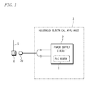
- FIG. 1 is a diagram showing the schematic configuration of a power line communication device (hereinafter referred to as a PLC modem) and a power supply circuit with a communication function based on power line communication according to one embodiment of the present invention. That is, PLC modem 1 is installed in power supply circuit 2, and power supply circuit 2 is installed in household electrical appliance 3, for example. By plug 3p connected to the primary side of power supply circuit 2 being inserted into outlet 4, power supply circuit 2 is supplied with a commercial AC voltage (AC 100 V) from power line 5, and PLC modem 1 can perform the power line communication.
- AC 100 V commercial AC voltage
- FIG. 2 is a circuit diagram showing the internal configuration of power supply circuit 2.
- Power supply circuit 2 uses the commercial AC voltage as the input voltage, and provides a prescribed DC output voltage (for example, DC 16 V) by performing rectification and AC/DC conversion by switching.
- DC output voltage for example, DC 16 V
- power supply circuit 2 structures a forward converter by connecting bridge circuit 21 structured by four diodes, a capacitor Cs used for rectification, LC parallel circuit 22, semiconductor switching element Sx, transformer 23, two diodes 24 and 25, choke coil 26, and smoothing capacitor 27, as shown in the drawing.
- LC parallel circuit 22 is made up of inductor Lx (inductance: Lx) and capacitor Cx (capacitance: Cx) connected in parallel to each other.
- Lx inductance
- Cx capacitor
- the foregoing components except for LC parallel circuit 22 are inherently required as a power supply circuit. It is to be noted that, the function of diodes 21, 24, and 25 can be realized by replacing with the transistors such as FETs and performing synchronous rectification.
- semiconductor switching element Sx a transistor suitable for switching at high frequencies (2 MHz or more), or a junction FET, a MOS-FET and the like are used.
- driver unit 29 and modulator unit 12 are connected in parallel.
- Driver unit 29 operates upon reception of a drive instruction from switching control unit 28.
- Modulator unit 12 operates upon reception of a modulation instruction from digital communication processing unit 11.
- switching control unit 28 instructs the timing of switching performed by driver unit 29 and an unoccupied time (which will be detailed later) to digital communication processing unit 11, such that the output of driver unit 29 and the output of modulator unit 12 are not simultaneously provided.
- demodulator unit 13 is connected via high-pass filters 14 and 15. The output signal from demodulator unit 13 is sent to digital communication processing unit 11.
- choke coil 26 discharges the stored energy so as to avoid variations in the current, and the current flows through the load via diode 25. Through the repetition of this procedure, the power is supplied to the load.
- the switching frequency is of relative low frequencies, i.e., about several ten kHz to several hundred kHz.
- reception a signal of the power line communication (high frequencies of 2 MHz to 30 MHz) imposed on the power line is demodulated by demodulator unit 13 via high-pass filters 14 and 15.
- the demodulated signal is decoded by digital communication processing unit 11.
- transmission is carried out by switching semiconductor switching element Sx by digital communication processing unit 11 via modulator unit 12. The switching is carried out at a high frequency of 2 MHz or more.
- FIG. 3A is a diagram schematically showing one example of a pulse signal (transmission signal) that drives the semiconductor switching element Sx for the power line communication.
- an ON state is entered at the start of a cycle t and an OFF state is entered at the time point of 1/2 cycle, it represents "0".
- an ON state is entered at the time point of 1/2 cycle and an OFF state is entered at the time point at the end of the one cycle, it represents "1".
- modulator unit 12 when the signal (information) of the power line communication to be transmitted is "00101", modulator unit 12 outputs a pulse signal shown in FIG. 3A .
- FIG. 3B is a diagram showing switching of power supply circuit 2 including the pulse signal shown in FIG. 3A .
- the inherent switching as a power supply circuit is carried out at a certain cycle ts based on a PWM (pulse width modulation) pulse shown as a power signal.
- the PWM pulse will not occupy the entire one cycle ts, and there is always an unoccupied time at each of the initial stage and the final stage of one cycle ts. Accordingly, using the unoccupied time, for example as shown in the drawing, a pulse signal of the power line communication shown in FIG. 3A is inserted at the initial stage of one cycle.
- the transmission time T is very short.
- digital communication processing unit 11 shown in FIG. 2 causes modulator unit 12 to operate in synchronization with switching control unit 28. Therefore, a signal can be inserted accurately in the targeted unoccupied time.
- semiconductor switching element Sx By the insertion of the signal described above, semiconductor switching element Sx is switched, and a signal of the power line communication is sent to power line 5 ( FIG. 1 ) via bridge circuit 21. In this manner, semiconductor switching element Sx plays a role of an oscillator that sends a signal of the power line communication betweentimes the inherent switching operations carried out for AC/DC conversion. Though the frequency of performing the signal insertion differs depending on the amount of information being transmitted, once every second will suffice when the information is, e.g., numerical value data. Accordingly, the effect of the signal insertion on the conversion efficiency as a power supply circuit can be suppressed to the negligible extent.
- PLC modem 1 or power supply circuit 2 having that function switches semiconductor switching element Sx in an ON/OFF mode having undergone the phase modulation based on the signal of the power line communication to be transmitted, to thereby achieve transmission of the signal to other PLC modem (or the power supply circuit or the household electrical appliance) via power line 5. Accordingly, a line driver (analog amplifier) or a high frequency transformer for sending a signal of the power line communication to the power line is not required. Thus, the transmission function of the power line communication can be realized with a simplified and cost-effective circuit configuration.
- power supply circuit 2 eliminates the necessity of parallel use of a power supply unit dedicated to the power line communication function. Still further, since semiconductor switching element Sx of power supply circuit 2 can be used, the function of the power line communication can be realized with further simplified and cost-effective circuit configuration.
- the impedance of LC parallel circuit 22 becomes extremely great due to the parallel resonance. Accordingly, even when the impedance of the capacitor Cs approaches 0 at high frequencies, short-circuiting between rectified-voltage output terminals C-D in FIG. 2 can be prevented.
- the frequency used in the power line communication may be a single frequency. Alternatively, it may be a plurality of frequencies or OFDM (Orthogonal Frequency Division Multiplexing). However, when the frequency band being used is wide, LC parallel circuit 22 (one inductor Lx and one capacitor Cx) as shown in FIG. 2 is not suitable, and a plurality of LC parallel circuits differing in resonance frequency must further be connected in parallel.
- transistor Sx in a case where a transistor is used as semiconductor switching element Sx, it is preferable to use an SiC transistor, a GaN transistor, or a diamond transistor. These transistors all involve just a small switching loss. Therefore, even when the switching for the power line communication is added to the inherent switching, a reduction in the conversion efficiency as a power supply circuit can be suppressed.
- power supply circuit 2 with a communication function as described above is integrated in modules (e.g., finished parts that are stored in a case or the like as the power supply unit).
- modules e.g., finished parts that are stored in a case or the like as the power supply unit.
- the function of the power line communication can be added with ease.
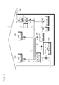
- FIG. 4 is a diagram showing one example of a home area network based on the power line communication.
- PLC modem 100 is connected to ONU (Optical Network Unit) 101 provided at the end of optical fiber 102.
- Power lines (domestic wiring) 5 of the home area are connected to one another through distribution switchboard 6.
- Distribution switchboard 5 is connected to an external power line via incoming line 7. At several points in power lines 5, outlets 4 are provided.
- power lines 5 stretched in the home area can be used as signal transmission paths based on the power line communication.
- electric appliances such as various home area household electrical appliances having installed therein power supply circuit 2 with the communication function as described above, to outlets 4, a LAN based on the power lines can be structured.
- air conditioners 301 to 303, television set 304, refrigerator 305, and central control and monitoring device 306 are the electric appliances having installed therein power supply circuit 2 with the communication function.
- Personal computer 307 is connected to PLC modem 100 so as to be capable of establishing communication. However, installing power supply circuit 2 with the communication function in personal computer 307, it is possible to establish communication via the power line.
- the current passing through incoming line 7 can be detected by current detector 8, and the output is sent to central control and monitoring device 306.
- personal computer 307 can establish an Internet connection through PLC modem 100 and ONU 101 via optical fiber 102.
- television set 304 is capable of receiving video distribution from optical fiber 102 via power line 5, for example.
- the home area network is structured for the purpose of controlling or monitoring the electric power.
- the target of control and monitoring is air conditioners whose power consumption is great.
- Air conditioners 301 to 303 have a function of providing information on the power consumption of themselves, and the information is sent to each power line 5 using the function of PLC modem 1 installed in power supply circuit 2.
- air conditioners 301 to 303 each have a function of externally receiving a signal that controls the operation of air conditioners 301 to 303, and they can receive the signal by the function of PLC modem 1 installed in power supply circuit 2.
- central control and monitoring device 306 is capable of receiving a signal from power line 5 using the function of PLC modem 1 installed in power supply circuit 2. Accordingly, it is capable of monitoring the power consumption of air conditioners 301 to 303 in the home area, and having it displayed as necessary. Further, central control and monitoring device 306 is capable of detecting the power consumption of the whole home area, based on the output of current detector 8. Still further, central control and monitoring device 306 has information on the acceptable power consumption (which is preset as the maximum power that can be used from the viewpoint of saving energy, for example) in the home area.
- the central control and monitoring device 306 stops at least one of operating air conditioners 301 to 303. Specifically, central control and monitoring device 306 transmits a stop signal to the air conditioner desired to be stopped, and the air conditioner receiving the signal can stop its operation by causing semiconductor switching element Sx of power supply circuit 2 to enter an OFF state continuously. Further, when the power consumption of the home area reduces and becomes significantly smaller than the acceptable power consumption, the stopped air conditioner can be activated again. In this manner, the household electrical appliance can remotely be controlled based on the power line communication.
- central control and monitoring device 306 is one example of the management appliance as to the control and monitoring of the electric power in the network. Such a function can also be realized by a personal computer. Further, the control and monitoring system structured with such a management appliance and an electric appliance being the target of control and monitoring can be applied to various electric appliances as such targets, without being limited to air conditioners. Still further, such a control and monitoring system can be structured at an office or a factory, without being limited to the home area.
- the present communication scheme is applicable not only to AC power supply lines, but also to DC power supply lines by dispensing with diode (sic) 21. Further, it is also applicable to FSK, QPSK, QAM, OFDM, SS (Spread Spectrum) modulation, without being limited to phase modulation.
- a line driver or a high frequency transformer for sending a signal of the power line communication to the power line can be dispensed with.
- the transmission function of the power line communication can be realized with a simplified and inexpensive circuit configuration.
- the power supply circuit with the communication function of the present invention in addition to the advantage that the line driver or the high frequency transformer for sending a signal of the power line communication to the power line can be dispensed with, use of the power supply circuit makes it possible to provide a power supply circuit that realizes the function of the power line communication with further simplified and cost-effective circuit configuration. The same holds true for the electric appliance and the control and monitoring system of the present invention.
Landscapes
- Engineering & Computer Science (AREA)
- Power Engineering (AREA)
- Computer Networks & Wireless Communication (AREA)
- Signal Processing (AREA)
- Cable Transmission Systems, Equalization Of Radio And Reduction Of Echo (AREA)
- Selective Calling Equipment (AREA)
- Remote Monitoring And Control Of Power-Distribution Networks (AREA)
Abstract
Description
- The present invention relates to a power line communication device that uses a power line as a signal transmission path, a power supply circuit having installed therein a function of power line communication, an electric appliance, and a control and monitoring system.
- The technique of structuring a network in a home area by the power line communication (PLC: Power Line Communication) is already in practical use. Such power line communication makes it possible to establish communication between PLC modems (power line communication devices) each connected to an outlet, in which a power line (domestic wiring) is used as a signal transmission path. Accordingly, without the necessity of laying a dedicated communication cable in the home area, a wired LAN (local area network) can be structured (for example, see Non Patent Literature 1). To each PLC modem, an appliance having an information communication function, such as a personal computer, is connected via a communication line. Further, not being limited to the personal computer, it is also possible to connect a household electrical appliance, which has added functions of receiving external control and providing information externally, to the PLC modem, so as to be included in the network (for example, see Patent Literature 1).
- However, it is troublesome to purchase and install a PLC modem per household electrical appliance. Also, it is inconvenient that the PLC modem occupies one outlet. Further, there is a case where installation of the PLC modem is physically difficult, such as on a wall surface or the like. Accordingly, it is preferable that a household electrical appliance previously includes a PLC modem, from the viewpoint of functionality and of promoting the prevalence of the PLC.
-
FIG. 5 is a diagram showing a circuit configuration example of a case where a PLC modem is installed in a household electrical appliance. With reference to the drawing, householdelectrical appliance 63 often includespower supply circuit 62 for supplying a DC power supply voltage to an electronic circuit which is installed for a control purpose.Power supply circuit 62 converts a commercial AC voltage supplied viaplug 63p into a prescribed DC voltage.PLC modem 61 is connected in parallel on the primary side ofpower supply circuit 62, and is connected topower line 65 byplug 63p being inserted intooutlet 64. -
PLC modem 61 is structured with PLCmodem circuit unit 611,high frequency transformer 612 for coupling with the power line, andcapacitors 613. Further, PLCmodem circuit unit 611 is structured with a digital communication processing unit, a modulator unit, a demodulator unit, and a line driver (analog amplifier) and the like, each of which is not shown. - As described above, when
PLC modem 61 is installed in householdelectrical appliance 63, there is a problem that householdelectrical appliance 63 is associated with complication of the circuitry and an increase in costs. Accordingly, how to simplify the circuitry and suppress in an increase in the cost becomes the problem to be solved. - Patent Literature 1: Japanese Publication of Unexamined Patent Application No.
2008-48012 FIG. 1 andFIG. 2 ) - Non Patent Literature 1: "Current State of Power Line Transmission (PLC: Power Line Communication)", Kiyoshi ETO, Interface, pages 70 to 81, CQ Publishing Co., Ltd., September, 2000
- In consideration of the problem stated above, an object of the present invention is to realize a transmission function of power line communication with a further simplified and cost-effective circuit configuration in a PLC modem installed in an electric appliance such as a household electrical appliance or the like.
- (1) The present invention is a power line communication device that uses a power line as a signal transmission path. The power line communication device includes: a semiconductor switching element that is present on an electric circuit connected to the power line; and a modulator unit that controls ON/OFF operations of the semiconductor switching element, to thereby cause a communication signal of a modulated rectangular wave to be output to the power line for a prescribed period.
- With the power line communication device structured as above, by switching the semiconductor switching element in the ON/OFF operation mode modulated based on a signal of the power line communication to be transmitted, the signal can be transmitted to other power line communication device via the power line. Accordingly, a line driver (analog amplifier) or a high frequency transformer for sending a signal of the power line communication on a power line is not required.
- (2) Further, in the power line communication device, the semiconductor switching element may also be used for performing switching in a power supply circuit supplied with an AC voltage from the power line, and the modulator unit may cause the semiconductor switching element to output the communication signal in an unoccupied time not being occupied with a power signal from the power supply circuit.
In this case, the power line communication device can be structured using the power supply circuit. - (3) On the other hand, the present invention is a power supply circuit that performs an AC/DC conversion by switching based on an AC voltage supplied from a power line. The power supply circuit includes: a semiconductor switching element that performs the switching; a demodulator unit that extracts and demodulates a signal of power line communication that is transmitted using the power line as a signal transmission path; and a modulator unit that uses an unoccupied time of switching for the AC/DC conversion to control ON/OFF operations of the semiconductor switching element, to thereby cause a communication signal of a modulated rectangular wave to be output to the power line for a prescribed period.
- With the power supply circuit with the communication function structured as above, by switching the semiconductor switching element in the ON/OFF operation mode having undergone the phase modulation based on a signal of the power line communication to be transmitted, a signal of the power line communication can be transmitted via the power line. Accordingly, a line driver or a high frequency transformer for sending a signal of the power line communication on the power line is not required. Further, use of the power supply circuit eliminates the necessity of parallel use of a power supply unit dedicated to the power line communication function. Still further, the semiconductor switching element of the power supply circuit can be used.
- (4) Further, in the power supply circuit with a communication function described in (3), it is preferable that, in series to a capacitor that is used for rectification in the power supply circuit, an LC parallel circuit made up of an inductor and a capacitor is inserted, and the LC parallel circuit has its inductance and capacitance set such that parallel resonance occurs at a switching frequency for the power line communication.
In this case, since the impedance of the LC parallel circuit becomes extremely great due to the parallel resonance, short-circuiting between the rectified-voltage output terminals can be prevented. - (5) Further, in the power supply circuit with a communication function described in (3), it is preferable that the semiconductor switching element uses one of an SiC transistor, a GaN transistor, and a diamond transistor.
In this case, these transistors all involve just a small switching loss. Therefore, even when the switching for the power line communication is added to the inherent switching, a reduction in the conversion efficiency as a power supply circuit can be suppressed. - (6) Further, the power supply circuit with a communication function described in (3) may be integrated into modules so as to be installable in an electric appliance.
In this case, by installing the power supply circuit integrated as modules in various electric appliances, the function of the power line communication can be added with ease. - (7) Further, an electric appliance of the present invention having installed therein the power supply circuit with a communication function described in (3) may include information on its own power consumption in the communication signal.
In this case, the information on the power consumption can easily be provided to a management appliance (a central control and monitoring device, a personal computer or the like). - (8) Further, an electric appliance of the present invention having installed therein the power supply circuit with a communication function described in (3) may control its own operation or perform its own electric power management based on a signal of the power line communication obtained by modulation.
In this case, the electric appliance can be the target of the remote control or the electric power management based on the power line communication. - (9) Further, the present invention as a control and monitoring system structures a network of power line communication with: an electric appliance that has installed therein the power supply circuit with a communication function described in (3), that includes information on its own power consumption in the communication signal, and that is capable of controlling its own operation or performing its own electric power management based on a signal of the power line communication obtained by modulation; and a management appliance that has the function of the power line communication. The management appliance controls and monitors information of the electric appliance.
In this case, without the necessity of additionally providing a line dedicated to communication, a management appliance (a central control and monitoring device, a personal computer or the like) can centrally control or monitor electric appliances. -
-
FIG. 1 is a diagram showing the schematic configuration of a power line communication device (PLC modem) and a power supply circuit with a communication function based on power line communication according to one embodiment of the present invention; -
FIG. 2 is a circuit diagram showing the internal configuration of the power supply circuit; -
FIG. 3A is a diagram schematically showing one example of a pulse signal that drives a semiconductor switching element for power line communication, andFIG. 3B is a diagram showing switching of a power supply circuit, in which the pulse signal shown inFIG. 3A is included; -
FIG. 4 is a diagram showing one example of a home area network based on the power line communication; and -
FIG. 5 is a diagram showing a circuit configuration example in a case where a PLC modem is included in a household electrical appliance. -
FIG. 1 is a diagram showing the schematic configuration of a power line communication device (hereinafter referred to as a PLC modem) and a power supply circuit with a communication function based on power line communication according to one embodiment of the present invention. That is,PLC modem 1 is installed inpower supply circuit 2, andpower supply circuit 2 is installed in householdelectrical appliance 3, for example. Byplug 3p connected to the primary side ofpower supply circuit 2 being inserted intooutlet 4,power supply circuit 2 is supplied with a commercial AC voltage (AC 100 V) frompower line 5, andPLC modem 1 can perform the power line communication. -
FIG. 2 is a circuit diagram showing the internal configuration ofpower supply circuit 2.Power supply circuit 2 uses the commercial AC voltage as the input voltage, and provides a prescribed DC output voltage (for example, DC 16 V) by performing rectification and AC/DC conversion by switching. Specifically,power supply circuit 2 structures a forward converter by connectingbridge circuit 21 structured by four diodes, a capacitor Cs used for rectification, LCparallel circuit 22, semiconductor switching element Sx,transformer 23, twodiodes choke coil 26, and smoothingcapacitor 27, as shown in the drawing. - LC
parallel circuit 22 is made up of inductor Lx (inductance: Lx) and capacitor Cx (capacitance: Cx) connected in parallel to each other. The foregoing components except for LCparallel circuit 22 are inherently required as a power supply circuit.
It is to be noted that, the function ofdiodes - Further, as semiconductor switching element Sx, a transistor suitable for switching at high frequencies (2 MHz or more), or a junction FET, a MOS-FET and the like are used. To the control terminal (base, gate) of semiconductor switching element Sx,
driver unit 29 andmodulator unit 12 are connected in parallel.Driver unit 29 operates upon reception of a drive instruction from switchingcontrol unit 28.Modulator unit 12 operates upon reception of a modulation instruction from digitalcommunication processing unit 11. - Further, switching
control unit 28 instructs the timing of switching performed bydriver unit 29 and an unoccupied time (which will be detailed later) to digitalcommunication processing unit 11, such that the output ofdriver unit 29 and the output ofmodulator unit 12 are not simultaneously provided. As shown in the drawing, to the opposite ends of LCparallel circuit 22,demodulator unit 13 is connected via high-pass filters demodulator unit 13 is sent to digitalcommunication processing unit 11. - First, a description will be given of an inherent function of the power supply circuit in
power supply circuit 2. When semiconductor switching element Sx in an OFF state enters an ON state by the output ofdriver unit 29, by the voltage rectified bybridge circuit 21, a counter electromotive force is generated at the primary-side winding oftransformer 23, and an induced electromotive force is generated at the secondary-side winding. Thus, a current flows through a load (not shown) viadiode 24, and the energy is stored inchoke coil 26. - Next, when semiconductor switching element Sx enters an OFF state, choke
coil 26 discharges the stored energy so as to avoid variations in the current, and the current flows through the load viadiode 25. Through the repetition of this procedure, the power is supplied to the load. The switching frequency is of relative low frequencies, i.e., about several ten kHz to several hundred kHz. - Next, a description will be given of the function of the power line communication in
power supply circuit 2.
First, as to reception, a signal of the power line communication (high frequencies of 2 MHz to 30 MHz) imposed on the power line is demodulated bydemodulator unit 13 via high-pass filters communication processing unit 11.
On the other hand, transmission is carried out by switching semiconductor switching element Sx by digitalcommunication processing unit 11 viamodulator unit 12. The switching is carried out at a high frequency of 2 MHz or more. -
FIG. 3A is a diagram schematically showing one example of a pulse signal (transmission signal) that drives the semiconductor switching element Sx for the power line communication. This signal is a digital signal having undergone the phase modulation. That is, the signal basically represents information of two bits based on the change in the timing of ON/OFF of the pulse (rectangular wave) in a unit time (= one cycle t). When an ON state is entered at the start of a cycle t and an OFF state is entered at the time point of 1/2 cycle, it represents "0". Conversely, when an ON state is entered at the time point of 1/2 cycle and an OFF state is entered at the time point at the end of the one cycle, it represents "1". - For example, when the signal (information) of the power line communication to be transmitted is "00101",
modulator unit 12 outputs a pulse signal shown inFIG. 3A . Thus,modulator unit 12 causes semiconductor switching element Sx to turn ON/OFF within a unit time (= t) at a certain cycle t during a prescribed period T, and carries out phase modulation by changing the timing of causing ON/OFF in one cycle t based on the signal of the power line communication to be transmitted. -
FIG. 3B is a diagram showing switching ofpower supply circuit 2 including the pulse signal shown inFIG. 3A . The inherent switching as a power supply circuit is carried out at a certain cycle ts based on a PWM (pulse width modulation) pulse shown as a power signal. The PWM pulse will not occupy the entire one cycle ts, and there is always an unoccupied time at each of the initial stage and the final stage of one cycle ts. Accordingly, using the unoccupied time, for example as shown in the drawing, a pulse signal of the power line communication shown inFIG. 3A is inserted at the initial stage of one cycle. - It is to be noted that, as described above, since the signal frequency of the power line communication is of far higher frequencies than the inherent switching frequency of the power supply circuit, the transmission time T is very short. Further, digital
communication processing unit 11 shown inFIG. 2 causes modulator unit 12 to operate in synchronization with switchingcontrol unit 28. Therefore, a signal can be inserted accurately in the targeted unoccupied time. - By the insertion of the signal described above, semiconductor switching element Sx is switched, and a signal of the power line communication is sent to power line 5 (
FIG. 1 ) viabridge circuit 21. In this manner, semiconductor switching element Sx plays a role of an oscillator that sends a signal of the power line communication betweentimes the inherent switching operations carried out for AC/DC conversion.
Though the frequency of performing the signal insertion differs depending on the amount of information being transmitted, once every second will suffice when the information is, e.g., numerical value data. Accordingly, the effect of the signal insertion on the conversion efficiency as a power supply circuit can be suppressed to the negligible extent. - As described above,
PLC modem 1 orpower supply circuit 2 having that function switches semiconductor switching element Sx in an ON/OFF mode having undergone the phase modulation based on the signal of the power line communication to be transmitted, to thereby achieve transmission of the signal to other PLC modem (or the power supply circuit or the household electrical appliance) viapower line 5. Accordingly, a line driver (analog amplifier) or a high frequency transformer for sending a signal of the power line communication to the power line is not required. Thus, the transmission function of the power line communication can be realized with a simplified and cost-effective circuit configuration. - Further, use of
power supply circuit 2 eliminates the necessity of parallel use of a power supply unit dedicated to the power line communication function. Still further, since semiconductor switching element Sx ofpower supply circuit 2 can be used, the function of the power line communication can be realized with further simplified and cost-effective circuit configuration. - It is to be noted that, LC
parallel circuit 22 has its inductance and capacitance set such that parallel resonance occurs at the switching frequency for power line communication. That is,
where fs is the switching frequency for the power line communication. In this case, the impedance of LCparallel circuit 22 becomes extremely great due to the parallel resonance. Accordingly, even when the impedance of the capacitor Cs approaches 0 at high frequencies, short-circuiting between rectified-voltage output terminals C-D inFIG. 2 can be prevented. - Further, it is necessary to adjust the Q-value of the resonance of Lx and Cx such that the common mode current flowing through the input terminals A and B shown in
FIG. 2 falls within a range of acceptable values (2 to 15 MHz: 30 dBµA, 15 to 30 MHz: 20 dBµA) of the power line communication prescribed by the Radio Law.
It is to be noted that, the frequency used in the power line communication may be a single frequency. Alternatively, it may be a plurality of frequencies or OFDM (Orthogonal Frequency Division Multiplexing). However, when the frequency band being used is wide, LC parallel circuit 22 (one inductor Lx and one capacitor Cx) as shown inFIG. 2 is not suitable, and a plurality of LC parallel circuits differing in resonance frequency must further be connected in parallel. - It is to be noted that, in a case where a transistor is used as semiconductor switching element Sx, it is preferable to use an SiC transistor, a GaN transistor, or a diamond transistor. These transistors all involve just a small switching loss. Therefore, even when the switching for the power line communication is added to the inherent switching, a reduction in the conversion efficiency as a power supply circuit can be suppressed.
- It is to be noted that, it is preferable that
power supply circuit 2 with a communication function as described above is integrated in modules (e.g., finished parts that are stored in a case or the like as the power supply unit).
In this case, by installingpower supply circuit 2 integrated as modules to various household electrical appliances or other electric appliances, the function of the power line communication can be added with ease. -
FIG. 4 is a diagram showing one example of a home area network based on the power line communication. In this house H,PLC modem 100 is connected to ONU (Optical Network Unit) 101 provided at the end ofoptical fiber 102. Power lines (domestic wiring) 5 of the home area are connected to one another throughdistribution switchboard 6.Distribution switchboard 5 is connected to an external power line via incoming line 7. At several points inpower lines 5,outlets 4 are provided. - By connecting
PLC modem 100 tooutlet 4,power lines 5 stretched in the home area can be used as signal transmission paths based on the power line communication. Further, by connecting electric appliances, such as various home area household electrical appliances having installed thereinpower supply circuit 2 with the communication function as described above, tooutlets 4, a LAN based on the power lines can be structured. Here, for example,air conditioners 301 to 303,television set 304,refrigerator 305, and central control and monitoring device 306 are the electric appliances having installed thereinpower supply circuit 2 with the communication function. -
Personal computer 307 is connected toPLC modem 100 so as to be capable of establishing communication. However, installingpower supply circuit 2 with the communication function inpersonal computer 307, it is possible to establish communication via the power line. The current passing through incoming line 7 can be detected bycurrent detector 8, and the output is sent to central control and monitoring device 306. - In the configuration as shown in
FIG. 4 ,personal computer 307 can establish an Internet connection throughPLC modem 100 andONU 101 viaoptical fiber 102. Further,television set 304 is capable of receiving video distribution fromoptical fiber 102 viapower line 5, for example. - Further, the home area network is structured for the purpose of controlling or monitoring the electric power. For example, the target of control and monitoring is air conditioners whose power consumption is great.
Air conditioners 301 to 303 have a function of providing information on the power consumption of themselves, and the information is sent to eachpower line 5 using the function ofPLC modem 1 installed inpower supply circuit 2. Further,air conditioners 301 to 303 each have a function of externally receiving a signal that controls the operation ofair conditioners 301 to 303, and they can receive the signal by the function ofPLC modem 1 installed inpower supply circuit 2. - On the other hand, central control and monitoring device 306 is capable of receiving a signal from
power line 5 using the function ofPLC modem 1 installed inpower supply circuit 2. Accordingly, it is capable of monitoring the power consumption ofair conditioners 301 to 303 in the home area, and having it displayed as necessary. Further, central control and monitoring device 306 is capable of detecting the power consumption of the whole home area, based on the output ofcurrent detector 8. Still further, central control and monitoring device 306 has information on the acceptable power consumption (which is preset as the maximum power that can be used from the viewpoint of saving energy, for example) in the home area. - When the power consumption of the home area exceeds the acceptable power consumption, the central control and monitoring device 306 stops at least one of operating
air conditioners 301 to 303. Specifically, central control and monitoring device 306 transmits a stop signal to the air conditioner desired to be stopped, and the air conditioner receiving the signal can stop its operation by causing semiconductor switching element Sx ofpower supply circuit 2 to enter an OFF state continuously. Further, when the power consumption of the home area reduces and becomes significantly smaller than the acceptable power consumption, the stopped air conditioner can be activated again. In this manner, the household electrical appliance can remotely be controlled based on the power line communication. - It is to be noted that, central control and monitoring device 306 is one example of the management appliance as to the control and monitoring of the electric power in the network. Such a function can also be realized by a personal computer. Further, the control and monitoring system structured with such a management appliance and an electric appliance being the target of control and monitoring can be applied to various electric appliances as such targets, without being limited to air conditioners. Still further, such a control and monitoring system can be structured at an office or a factory, without being limited to the home area.
- It is to be noted that the embodiment disclosed herein should be construed as an example in every respect, and not as a limitation. It is intended that the scope of the present invention is shown by the description of the claims, and includes any modification being equivalent to the meaning and the scope of the description of the claims.
For example, the present communication scheme is applicable not only to AC power supply lines, but also to DC power supply lines by dispensing with diode (sic) 21. Further, it is also applicable to FSK, QPSK, QAM, OFDM, SS (Spread Spectrum) modulation, without being limited to phase modulation. - With the power line communication device of the present invention, a line driver or a high frequency transformer for sending a signal of the power line communication to the power line can be dispensed with. Thus, the transmission function of the power line communication can be realized with a simplified and inexpensive circuit configuration.
Further, with the power supply circuit with the communication function of the present invention, in addition to the advantage that the line driver or the high frequency transformer for sending a signal of the power line communication to the power line can be dispensed with, use of the power supply circuit makes it possible to provide a power supply circuit that realizes the function of the power line communication with further simplified and cost-effective circuit configuration. The same holds true for the electric appliance and the control and monitoring system of the present invention.
Claims (9)
- A power line communication device that uses a power line as a signal transmission path, comprising:a semiconductor switching element that is present on an electric circuit connected to the power line; anda modulator unit that controls ON/OFF operations of the semiconductor switching element, to thereby cause a communication signal of a modulated rectangular wave to be output to the power line for a prescribed period.
- The power line communication device according to claim 1, wherein
the semiconductor switching element is also used for performing switching in a power supply circuit supplied with an AC voltage from the power line, and
the modulator unit causes the semiconductor switching element to output the communication signal in an unoccupied time not being occupied with a power signal from the power supply circuit. - A power supply circuit with a communication function that performs an AC/DC conversion by switching based on an AC voltage supplied from a power line, comprising:a semiconductor switching element that performs the switching;a demodulator unit that extracts and demodulates a signal of power line communication that is transmitted using the power line as a signal transmission path; anda modulator unit that uses an unoccupied time of switching for the AC/DC conversion to control ON/OFF operations of the semiconductor switching element, to thereby cause a communication signal of a modulated rectangular wave to be output to the power line for a prescribed period.
- The power supply circuit with a communication function according to claim 3, wherein
in series to a capacitor that is used for rectification in the power supply circuit, an LC parallel circuit made up of an inductor and a capacitor is inserted, and
the LC parallel circuit has its inductance and capacitance set such that parallel resonance occurs at a switching frequency for the power line communication. - The power supply circuit with a communication function according to claim 3, wherein
the semiconductor switching element uses one of an SiC transistor, a GaN transistor, and a diamond transistor. - The power supply circuit with a communication function according to claim 3, wherein
the power supply circuit is integrated into modules so as to be installable in an electric appliance. - An electric appliance having installed therein the power supply circuit with a communication function according to claim 3, wherein
the electric appliance includes information on its own power consumption in the communication signal. - An electric appliance having installed therein the power supply circuit with a communication function according to claim 3, wherein
the electric appliance controls its own operation or performs its own electric power management based on a signal of the power line communication obtained by modulation. - A control and monitoring system structuring a network of power line communication with: an electric appliance that has installed therein the power supply circuit with a communication function according to claim 3, that includes information on its own power consumption in the communication signal, and that is capable of controlling its own operation or performing its own electric power management based on a signal of the power line communication obtained by modulation; and a management appliance that has the function of the power line communication, wherein
the management appliance controls the electric appliance and monitors the information of the electric appliance.
Applications Claiming Priority (2)
| Application Number | Priority Date | Filing Date | Title |
|---|---|---|---|
| JP2009183745A JP5432628B2 (en) | 2009-08-06 | 2009-08-06 | Power line communication device, power supply circuit with communication function, electrical equipment and control monitoring system |
| PCT/JP2010/063146 WO2011016466A1 (en) | 2009-08-06 | 2010-08-04 | Power line communication device, power supply circuit with communication function, electrical appliance, and control-monitoring system |
Publications (3)
| Publication Number | Publication Date |
|---|---|
| EP2464027A1 true EP2464027A1 (en) | 2012-06-13 |
| EP2464027A4 EP2464027A4 (en) | 2016-07-13 |
| EP2464027B1 EP2464027B1 (en) | 2017-09-27 |
Family
ID=43544361
Family Applications (1)
| Application Number | Title | Priority Date | Filing Date |
|---|---|---|---|
| EP10806465.0A Not-in-force EP2464027B1 (en) | 2009-08-06 | 2010-08-04 | Power line communication device, power supply circuit with communication function, electrical appliance, and control-monitoring system |
Country Status (6)
| Country | Link |
|---|---|
| US (1) | US9136911B2 (en) |
| EP (1) | EP2464027B1 (en) |
| JP (1) | JP5432628B2 (en) |
| CN (1) | CN102648587B (en) |
| TW (1) | TWI475816B (en) |
| WO (1) | WO2011016466A1 (en) |
Cited By (1)
| Publication number | Priority date | Publication date | Assignee | Title |
|---|---|---|---|---|
| EP3089372A1 (en) * | 2015-04-27 | 2016-11-02 | Deutsche Telekom AG | Assembly and method for integrated transmission of messages via electrical energy supply networks |
Families Citing this family (19)
| Publication number | Priority date | Publication date | Assignee | Title |
|---|---|---|---|---|
| JP5432628B2 (en) * | 2009-08-06 | 2014-03-05 | 住友電気工業株式会社 | Power line communication device, power supply circuit with communication function, electrical equipment and control monitoring system |
| JP5900944B2 (en) * | 2010-11-22 | 2016-04-06 | ソニー株式会社 | Power relay terminal, power relay method, power supply control device, power supply control method, and power supply control system |
| EP2672632A4 (en) * | 2011-03-10 | 2014-07-23 | Panasonic Corp | ONLINE BEARING CURRENT DEVICE, ONLINE BEARING CURRENT SYSTEM, ONLINE BEARING CURRENT METHOD, AND ONLINE CURRENT CURRENT PROGRAM |
| JP5758208B2 (en) * | 2011-06-09 | 2015-08-05 | 株式会社吉川アールエフセミコン | Power line transmission device |
| JP2013009574A (en) * | 2011-06-22 | 2013-01-10 | Csr Inc | Charging type electric/electronic system |
| US9014247B2 (en) * | 2011-10-14 | 2015-04-21 | Texas Instruments Incorporated | Communication on a pilot wire |
| JP5858528B2 (en) * | 2011-12-12 | 2016-02-10 | 住友電気工業株式会社 | Solar power generation apparatus and solar power generation system |
| WO2013151007A1 (en) | 2012-04-05 | 2013-10-10 | 三菱電機株式会社 | Charging communication system, charging control unit and charging station |
| CN103957033A (en) * | 2014-05-12 | 2014-07-30 | 东南大学 | Communication-line-free data transmission method between power electronic devices based on composite modulation |
| KR101586742B1 (en) * | 2014-09-26 | 2016-01-20 | (주)코콤 | Local communication system using an AC power line |
| GB2536907A (en) * | 2015-03-30 | 2016-10-05 | Lighting And Illumination Tech Experience Ltd | Controlling power to a load with signals along a power line |
| US10063316B2 (en) * | 2016-04-30 | 2018-08-28 | Nanoprecision Products, Inc. | Wall plate having a built-in modem for performing electrical-to-optical conversion, optical-to-electrical conversion and protocol-to-protocol conversion |
| CN105573282B (en) * | 2016-02-03 | 2020-03-17 | 京东方科技集团股份有限公司 | Household power grid |
| CN108302742B (en) * | 2018-04-13 | 2020-05-29 | 珠海格力电器股份有限公司 | Controller of air conditioning unit and air conditioner |
| US11005531B1 (en) * | 2020-04-13 | 2021-05-11 | Nxp B.V. | System and method for communicating over a single-wire transmission line |
| US11477283B2 (en) * | 2020-05-05 | 2022-10-18 | Dell Products L.P. | Remote server management using a power line network |
| CN115882897B (en) * | 2021-08-06 | 2025-07-08 | 国网北京市电力公司 | Power line loop communication method based on current-type rectifier bridge and reactive power variation |
| US12093196B2 (en) * | 2022-04-01 | 2024-09-17 | Intel Corporation | Power supply communications via a shared channel for performance management |
| CN116633391B (en) * | 2023-05-05 | 2026-04-10 | 深圳市旭日东方实业有限公司 | An isolated communication device |
Family Cites Families (28)
| Publication number | Priority date | Publication date | Assignee | Title |
|---|---|---|---|---|
| US4210901A (en) * | 1977-04-25 | 1980-07-01 | Westinghouse Electric Corp. | Signal repeater for a distribution network communication system |
| US4360881A (en) * | 1980-07-07 | 1982-11-23 | Martinson John R | Energy consumption control system and method |
| US4475209A (en) * | 1982-04-23 | 1984-10-02 | Westinghouse Electric Corp. | Regenerator for an intrabundle power-line communication system |
| US5227762A (en) * | 1990-10-26 | 1993-07-13 | Thomas Industries Inc. | Power line carrier controlled lighting system |
| JPH10255003A (en) * | 1997-03-13 | 1998-09-25 | Omron Corp | Reader / writer |
| AU2001258119A1 (en) * | 2000-05-09 | 2001-12-03 | Lumion Corporation | Ac power line signalling system |
| KR100446931B1 (en) * | 2002-04-30 | 2004-09-04 | 주식회사 두노시스템 | Adapter for using Power Line Communication |
| JP4423157B2 (en) * | 2004-10-06 | 2010-03-03 | キヤノン株式会社 | Power line communication apparatus and control method thereof |
| US7345998B2 (en) * | 2004-12-15 | 2008-03-18 | Smart Labs, Inc. | Mesh network of intelligent devices communicating via powerline and radio frequency |
| JP2006174181A (en) * | 2004-12-16 | 2006-06-29 | Alps Electric Co Ltd | Modem for power line communication |
| JP2007081845A (en) * | 2005-09-14 | 2007-03-29 | Fujitsu Ten Ltd | Sinusoidal signal generator |
| JP4708145B2 (en) * | 2005-10-05 | 2011-06-22 | パナソニック株式会社 | Power line communication device |
| CN101009501A (en) * | 2006-01-24 | 2007-08-01 | 黄勇 | A DC power line carrier communication method, system and lamp series using the system |
| JP2007221358A (en) * | 2006-02-15 | 2007-08-30 | Matsushita Electric Ind Co Ltd | Cable connector for power line communication |
| CN101090282A (en) * | 2006-06-15 | 2007-12-19 | 杭州瑞琦信息技术有限公司 | Power carrier communication circuit capable of overcome compensating capacitor |
| JP2008011645A (en) * | 2006-06-29 | 2008-01-17 | Toshiba Corp | POWER CONTROL DEVICE, ELECTRONIC DEVICE, AND OPERATION CONTROL METHOD |
| JP2008048012A (en) | 2006-08-11 | 2008-02-28 | Sumitomo Electric Ind Ltd | PLC network system and PLC modem |
| KR100790475B1 (en) * | 2006-09-22 | 2008-01-02 | 주식회사 애버드 | Data communication method and device using power line |
| US8049599B2 (en) * | 2006-12-29 | 2011-11-01 | Marvell World Trade Ltd. | Power control device |
| JP2008245408A (en) * | 2007-03-27 | 2008-10-09 | Toyota Motor Corp | Electric power system and electric vehicle |
| JP2009093125A (en) * | 2007-10-03 | 2009-04-30 | Institute Of National Colleges Of Technology Japan | Illumination, information display system and display method using multicolor light emitting element |
| US8284035B2 (en) * | 2008-09-26 | 2012-10-09 | Albeo Technologies, Inc. | Systems and methods for conveying information using a control signal referenced to alternating current (AC) power |
| JP4668315B2 (en) * | 2008-12-02 | 2011-04-13 | フェリカネットワークス株式会社 | Information processing apparatus, communication control method, and program |
| US8265197B2 (en) * | 2009-08-03 | 2012-09-11 | Texas Instruments Incorporated | OFDM transmission methods in three phase modes |
| JP5432628B2 (en) * | 2009-08-06 | 2014-03-05 | 住友電気工業株式会社 | Power line communication device, power supply circuit with communication function, electrical equipment and control monitoring system |
| KR101047511B1 (en) * | 2010-03-10 | 2011-07-07 | 최인숙 | Power line communication method for transmitting data signal by dividing power transmission section |
| JP5246383B2 (en) * | 2010-08-24 | 2013-07-24 | ソニー株式会社 | Transmitting apparatus, receiving apparatus, and communication system |
| JP5498347B2 (en) * | 2010-10-20 | 2014-05-21 | 株式会社メガチップス | PLC / power hybrid device and device with communication function |
-
2009
- 2009-08-06 JP JP2009183745A patent/JP5432628B2/en not_active Expired - Fee Related
-
2010
- 2010-08-04 EP EP10806465.0A patent/EP2464027B1/en not_active Not-in-force
- 2010-08-04 US US13/388,878 patent/US9136911B2/en not_active Expired - Fee Related
- 2010-08-04 CN CN201080034453.6A patent/CN102648587B/en not_active Expired - Fee Related
- 2010-08-04 WO PCT/JP2010/063146 patent/WO2011016466A1/en not_active Ceased
- 2010-08-05 TW TW099126028A patent/TWI475816B/en not_active IP Right Cessation
Non-Patent Citations (1)
| Title |
|---|
| See references of WO2011016466A1 * |
Cited By (1)
| Publication number | Priority date | Publication date | Assignee | Title |
|---|---|---|---|---|
| EP3089372A1 (en) * | 2015-04-27 | 2016-11-02 | Deutsche Telekom AG | Assembly and method for integrated transmission of messages via electrical energy supply networks |
Also Published As
| Publication number | Publication date |
|---|---|
| TW201119258A (en) | 2011-06-01 |
| JP2011040829A (en) | 2011-02-24 |
| JP5432628B2 (en) | 2014-03-05 |
| TWI475816B (en) | 2015-03-01 |
| CN102648587B (en) | 2015-07-15 |
| CN102648587A (en) | 2012-08-22 |
| EP2464027B1 (en) | 2017-09-27 |
| WO2011016466A1 (en) | 2011-02-10 |
| US9136911B2 (en) | 2015-09-15 |
| EP2464027A4 (en) | 2016-07-13 |
| US20120128081A1 (en) | 2012-05-24 |
Similar Documents
| Publication | Publication Date | Title |
|---|---|---|
| EP2464027B1 (en) | Power line communication device, power supply circuit with communication function, electrical appliance, and control-monitoring system | |
| US7889061B2 (en) | Power-line communication device | |
| KR101047511B1 (en) | Power line communication method for transmitting data signal by dividing power transmission section | |
| KR100378813B1 (en) | Circuit for reducing standby power of electric apparatus | |
| US20120120700A1 (en) | Method and Apparatus for Regulating AC-DC Adaptor for Low Current Drain | |
| US20190348867A1 (en) | Coupling Optimized Electrical Wireless Power Transmission | |
| CN104363675B (en) | Illuminator communication equipment and method | |
| CN105515616B (en) | A kind of direct current supply line carrier communication system and communication means | |
| WO2003026114B1 (en) | Universal energy supply system | |
| CN108429359A (en) | Wireless power transmitter with wide input voltage range and its operating method | |
| KR20140090669A (en) | A method for controlling a converter | |
| US20070297199A1 (en) | Multi-Resonance Converter | |
| TW201351903A (en) | Power line communication control system | |
| US9698868B2 (en) | Power line communication device | |
| US9294148B1 (en) | Power line communication system | |
| WO2015148998A1 (en) | Wireless power system | |
| WO2011136591A2 (en) | Indoor direct current power system and power line communication method thereof | |
| TWI840390B (en) | System for transferring electrical power to an electrical load | |
| KR101137824B1 (en) | Lamp Control System and its method With Power Line Communication | |
| KR101514520B1 (en) | Power supplying apparatus | |
| KR20010055158A (en) | Apparatus for power saving in set-top box | |
| JP3615668B2 (en) | Current supply circuit | |
| CN1435997A (en) | Low power consumption standby circuit for TV set | |
| KR101454486B1 (en) | Power supply having multiple outputs | |
| KR20170089350A (en) | Wirelessly power tranceiver |
Legal Events
| Date | Code | Title | Description |
|---|---|---|---|
| PUAI | Public reference made under article 153(3) epc to a published international application that has entered the european phase |
Free format text: ORIGINAL CODE: 0009012 |
|
| 17P | Request for examination filed |
Effective date: 20120202 |
|
| AK | Designated contracting states |
Kind code of ref document: A1 Designated state(s): AL AT BE BG CH CY CZ DE DK EE ES FI FR GB GR HR HU IE IS IT LI LT LU LV MC MK MT NL NO PL PT RO SE SI SK SM TR |
|
| DAX | Request for extension of the european patent (deleted) | ||
| RA4 | Supplementary search report drawn up and despatched (corrected) |
Effective date: 20160609 |
|
| RIC1 | Information provided on ipc code assigned before grant |
Ipc: H04B 3/56 20060101ALI20160603BHEP Ipc: H04B 3/54 20060101AFI20160603BHEP |
|
| GRAP | Despatch of communication of intention to grant a patent |
Free format text: ORIGINAL CODE: EPIDOSNIGR1 |
|
| STAA | Information on the status of an ep patent application or granted ep patent |
Free format text: STATUS: GRANT OF PATENT IS INTENDED |
|
| INTG | Intention to grant announced |
Effective date: 20170322 |
|
| GRAS | Grant fee paid |
Free format text: ORIGINAL CODE: EPIDOSNIGR3 |
|
| GRAA | (expected) grant |
Free format text: ORIGINAL CODE: 0009210 |
|
| STAA | Information on the status of an ep patent application or granted ep patent |
Free format text: STATUS: THE PATENT HAS BEEN GRANTED |
|
| AK | Designated contracting states |
Kind code of ref document: B1 Designated state(s): AL AT BE BG CH CY CZ DE DK EE ES FI FR GB GR HR HU IE IS IT LI LT LU LV MC MK MT NL NO PL PT RO SE SI SK SM TR |
|
| REG | Reference to a national code |
Ref country code: GB Ref legal event code: FG4D |
|
| REG | Reference to a national code |
Ref country code: CH Ref legal event code: EP |
|
| REG | Reference to a national code |
Ref country code: AT Ref legal event code: REF Ref document number: 932879 Country of ref document: AT Kind code of ref document: T Effective date: 20171015 |
|
| REG | Reference to a national code |
Ref country code: IE Ref legal event code: FG4D |
|
| REG | Reference to a national code |
Ref country code: DE Ref legal event code: R096 Ref document number: 602010045606 Country of ref document: DE |
|
| PG25 | Lapsed in a contracting state [announced via postgrant information from national office to epo] |
Ref country code: SE Free format text: LAPSE BECAUSE OF FAILURE TO SUBMIT A TRANSLATION OF THE DESCRIPTION OR TO PAY THE FEE WITHIN THE PRESCRIBED TIME-LIMIT Effective date: 20170927 Ref country code: HR Free format text: LAPSE BECAUSE OF FAILURE TO SUBMIT A TRANSLATION OF THE DESCRIPTION OR TO PAY THE FEE WITHIN THE PRESCRIBED TIME-LIMIT Effective date: 20170927 Ref country code: LT Free format text: LAPSE BECAUSE OF FAILURE TO SUBMIT A TRANSLATION OF THE DESCRIPTION OR TO PAY THE FEE WITHIN THE PRESCRIBED TIME-LIMIT Effective date: 20170927 Ref country code: FI Free format text: LAPSE BECAUSE OF FAILURE TO SUBMIT A TRANSLATION OF THE DESCRIPTION OR TO PAY THE FEE WITHIN THE PRESCRIBED TIME-LIMIT Effective date: 20170927 Ref country code: NO Free format text: LAPSE BECAUSE OF FAILURE TO SUBMIT A TRANSLATION OF THE DESCRIPTION OR TO PAY THE FEE WITHIN THE PRESCRIBED TIME-LIMIT Effective date: 20171227 |
|
| REG | Reference to a national code |
Ref country code: NL Ref legal event code: MP Effective date: 20170927 |
|
| REG | Reference to a national code |
Ref country code: LT Ref legal event code: MG4D |
|
| REG | Reference to a national code |
Ref country code: AT Ref legal event code: MK05 Ref document number: 932879 Country of ref document: AT Kind code of ref document: T Effective date: 20170927 |
|
| PG25 | Lapsed in a contracting state [announced via postgrant information from national office to epo] |
Ref country code: LV Free format text: LAPSE BECAUSE OF FAILURE TO SUBMIT A TRANSLATION OF THE DESCRIPTION OR TO PAY THE FEE WITHIN THE PRESCRIBED TIME-LIMIT Effective date: 20170927 Ref country code: GR Free format text: LAPSE BECAUSE OF FAILURE TO SUBMIT A TRANSLATION OF THE DESCRIPTION OR TO PAY THE FEE WITHIN THE PRESCRIBED TIME-LIMIT Effective date: 20171228 Ref country code: BG Free format text: LAPSE BECAUSE OF FAILURE TO SUBMIT A TRANSLATION OF THE DESCRIPTION OR TO PAY THE FEE WITHIN THE PRESCRIBED TIME-LIMIT Effective date: 20171227 |
|
| PG25 | Lapsed in a contracting state [announced via postgrant information from national office to epo] |
Ref country code: NL Free format text: LAPSE BECAUSE OF FAILURE TO SUBMIT A TRANSLATION OF THE DESCRIPTION OR TO PAY THE FEE WITHIN THE PRESCRIBED TIME-LIMIT Effective date: 20170927 |
|
| PG25 | Lapsed in a contracting state [announced via postgrant information from national office to epo] |
Ref country code: RO Free format text: LAPSE BECAUSE OF FAILURE TO SUBMIT A TRANSLATION OF THE DESCRIPTION OR TO PAY THE FEE WITHIN THE PRESCRIBED TIME-LIMIT Effective date: 20170927 Ref country code: ES Free format text: LAPSE BECAUSE OF FAILURE TO SUBMIT A TRANSLATION OF THE DESCRIPTION OR TO PAY THE FEE WITHIN THE PRESCRIBED TIME-LIMIT Effective date: 20170927 Ref country code: CZ Free format text: LAPSE BECAUSE OF FAILURE TO SUBMIT A TRANSLATION OF THE DESCRIPTION OR TO PAY THE FEE WITHIN THE PRESCRIBED TIME-LIMIT Effective date: 20170927 |
|
| PG25 | Lapsed in a contracting state [announced via postgrant information from national office to epo] |
Ref country code: EE Free format text: LAPSE BECAUSE OF FAILURE TO SUBMIT A TRANSLATION OF THE DESCRIPTION OR TO PAY THE FEE WITHIN THE PRESCRIBED TIME-LIMIT Effective date: 20170927 Ref country code: AT Free format text: LAPSE BECAUSE OF FAILURE TO SUBMIT A TRANSLATION OF THE DESCRIPTION OR TO PAY THE FEE WITHIN THE PRESCRIBED TIME-LIMIT Effective date: 20170927 Ref country code: IT Free format text: LAPSE BECAUSE OF FAILURE TO SUBMIT A TRANSLATION OF THE DESCRIPTION OR TO PAY THE FEE WITHIN THE PRESCRIBED TIME-LIMIT Effective date: 20170927 Ref country code: IS Free format text: LAPSE BECAUSE OF FAILURE TO SUBMIT A TRANSLATION OF THE DESCRIPTION OR TO PAY THE FEE WITHIN THE PRESCRIBED TIME-LIMIT Effective date: 20180127 Ref country code: SK Free format text: LAPSE BECAUSE OF FAILURE TO SUBMIT A TRANSLATION OF THE DESCRIPTION OR TO PAY THE FEE WITHIN THE PRESCRIBED TIME-LIMIT Effective date: 20170927 Ref country code: SM Free format text: LAPSE BECAUSE OF FAILURE TO SUBMIT A TRANSLATION OF THE DESCRIPTION OR TO PAY THE FEE WITHIN THE PRESCRIBED TIME-LIMIT Effective date: 20170927 |
|
| REG | Reference to a national code |
Ref country code: DE Ref legal event code: R097 Ref document number: 602010045606 Country of ref document: DE |
|
| PG25 | Lapsed in a contracting state [announced via postgrant information from national office to epo] |
Ref country code: DK Free format text: LAPSE BECAUSE OF FAILURE TO SUBMIT A TRANSLATION OF THE DESCRIPTION OR TO PAY THE FEE WITHIN THE PRESCRIBED TIME-LIMIT Effective date: 20170927 |
|
| PLBE | No opposition filed within time limit |
Free format text: ORIGINAL CODE: 0009261 |
|
| STAA | Information on the status of an ep patent application or granted ep patent |
Free format text: STATUS: NO OPPOSITION FILED WITHIN TIME LIMIT |
|
| PG25 | Lapsed in a contracting state [announced via postgrant information from national office to epo] |
Ref country code: PL Free format text: LAPSE BECAUSE OF FAILURE TO SUBMIT A TRANSLATION OF THE DESCRIPTION OR TO PAY THE FEE WITHIN THE PRESCRIBED TIME-LIMIT Effective date: 20170927 |
|
| 26N | No opposition filed |
Effective date: 20180628 |
|
| PG25 | Lapsed in a contracting state [announced via postgrant information from national office to epo] |
Ref country code: SI Free format text: LAPSE BECAUSE OF FAILURE TO SUBMIT A TRANSLATION OF THE DESCRIPTION OR TO PAY THE FEE WITHIN THE PRESCRIBED TIME-LIMIT Effective date: 20170927 |
|
| PG25 | Lapsed in a contracting state [announced via postgrant information from national office to epo] |
Ref country code: MC Free format text: LAPSE BECAUSE OF FAILURE TO SUBMIT A TRANSLATION OF THE DESCRIPTION OR TO PAY THE FEE WITHIN THE PRESCRIBED TIME-LIMIT Effective date: 20170927 |
|
| REG | Reference to a national code |
Ref country code: CH Ref legal event code: PL |
|
| PG25 | Lapsed in a contracting state [announced via postgrant information from national office to epo] |
Ref country code: LU Free format text: LAPSE BECAUSE OF NON-PAYMENT OF DUE FEES Effective date: 20180804 Ref country code: CH Free format text: LAPSE BECAUSE OF NON-PAYMENT OF DUE FEES Effective date: 20180831 Ref country code: LI Free format text: LAPSE BECAUSE OF NON-PAYMENT OF DUE FEES Effective date: 20180831 |
|
| REG | Reference to a national code |
Ref country code: BE Ref legal event code: MM Effective date: 20180831 |
|
| REG | Reference to a national code |
Ref country code: IE Ref legal event code: MM4A |
|
| PG25 | Lapsed in a contracting state [announced via postgrant information from national office to epo] |
Ref country code: IE Free format text: LAPSE BECAUSE OF NON-PAYMENT OF DUE FEES Effective date: 20180804 |
|
| PG25 | Lapsed in a contracting state [announced via postgrant information from national office to epo] |
Ref country code: FR Free format text: LAPSE BECAUSE OF NON-PAYMENT OF DUE FEES Effective date: 20180831 Ref country code: BE Free format text: LAPSE BECAUSE OF NON-PAYMENT OF DUE FEES Effective date: 20180831 |
|
| PG25 | Lapsed in a contracting state [announced via postgrant information from national office to epo] |
Ref country code: MT Free format text: LAPSE BECAUSE OF NON-PAYMENT OF DUE FEES Effective date: 20180804 |
|
| PG25 | Lapsed in a contracting state [announced via postgrant information from national office to epo] |
Ref country code: TR Free format text: LAPSE BECAUSE OF FAILURE TO SUBMIT A TRANSLATION OF THE DESCRIPTION OR TO PAY THE FEE WITHIN THE PRESCRIBED TIME-LIMIT Effective date: 20170927 |
|
| PG25 | Lapsed in a contracting state [announced via postgrant information from national office to epo] |
Ref country code: HU Free format text: LAPSE BECAUSE OF FAILURE TO SUBMIT A TRANSLATION OF THE DESCRIPTION OR TO PAY THE FEE WITHIN THE PRESCRIBED TIME-LIMIT; INVALID AB INITIO Effective date: 20100804 Ref country code: PT Free format text: LAPSE BECAUSE OF FAILURE TO SUBMIT A TRANSLATION OF THE DESCRIPTION OR TO PAY THE FEE WITHIN THE PRESCRIBED TIME-LIMIT Effective date: 20170927 |
|
| PG25 | Lapsed in a contracting state [announced via postgrant information from national office to epo] |
Ref country code: CY Free format text: LAPSE BECAUSE OF FAILURE TO SUBMIT A TRANSLATION OF THE DESCRIPTION OR TO PAY THE FEE WITHIN THE PRESCRIBED TIME-LIMIT Effective date: 20170927 Ref country code: MK Free format text: LAPSE BECAUSE OF NON-PAYMENT OF DUE FEES Effective date: 20170927 |
|
| PG25 | Lapsed in a contracting state [announced via postgrant information from national office to epo] |
Ref country code: AL Free format text: LAPSE BECAUSE OF FAILURE TO SUBMIT A TRANSLATION OF THE DESCRIPTION OR TO PAY THE FEE WITHIN THE PRESCRIBED TIME-LIMIT Effective date: 20170927 |
|
| PGFP | Annual fee paid to national office [announced via postgrant information from national office to epo] |
Ref country code: GB Payment date: 20210701 Year of fee payment: 12 Ref country code: DE Payment date: 20210630 Year of fee payment: 12 |
|
| REG | Reference to a national code |
Ref country code: DE Ref legal event code: R119 Ref document number: 602010045606 Country of ref document: DE |
|
| GBPC | Gb: european patent ceased through non-payment of renewal fee |
Effective date: 20220804 |
|
| PG25 | Lapsed in a contracting state [announced via postgrant information from national office to epo] |
Ref country code: DE Free format text: LAPSE BECAUSE OF NON-PAYMENT OF DUE FEES Effective date: 20230301 |
|
| PG25 | Lapsed in a contracting state [announced via postgrant information from national office to epo] |
Ref country code: GB Free format text: LAPSE BECAUSE OF NON-PAYMENT OF DUE FEES Effective date: 20220804 |