KR20170089350A - Wirelessly power tranceiver - Google Patents
Wirelessly power tranceiver Download PDFInfo
- Publication number
- KR20170089350A KR20170089350A KR1020160009647A KR20160009647A KR20170089350A KR 20170089350 A KR20170089350 A KR 20170089350A KR 1020160009647 A KR1020160009647 A KR 1020160009647A KR 20160009647 A KR20160009647 A KR 20160009647A KR 20170089350 A KR20170089350 A KR 20170089350A
- Authority
- KR
- South Korea
- Prior art keywords
- bridge circuit
- converter
- power
- switch
- resonant
- Prior art date
Links
- 230000005540 biological transmission Effects 0.000 claims abstract description 50
- 230000002457 bidirectional effect Effects 0.000 claims abstract description 33
- 239000003990 capacitor Substances 0.000 claims description 46
- 238000000034 method Methods 0.000 claims description 9
- 239000004065 semiconductor Substances 0.000 claims 2
- 238000010586 diagram Methods 0.000 description 25
- 230000003071 parasitic effect Effects 0.000 description 8
- 238000005516 engineering process Methods 0.000 description 3
- 238000007792 addition Methods 0.000 description 1
- 238000004891 communication Methods 0.000 description 1
- 238000007599 discharging Methods 0.000 description 1
- 230000000694 effects Effects 0.000 description 1
- 230000014509 gene expression Effects 0.000 description 1
- 230000006698 induction Effects 0.000 description 1
- 239000011159 matrix material Substances 0.000 description 1
- 238000012986 modification Methods 0.000 description 1
- 230000004048 modification Effects 0.000 description 1
- 238000009774 resonance method Methods 0.000 description 1
- 238000006467 substitution reaction Methods 0.000 description 1
Images


Classifications
-
- H—ELECTRICITY
- H02—GENERATION; CONVERSION OR DISTRIBUTION OF ELECTRIC POWER
- H02J—CIRCUIT ARRANGEMENTS OR SYSTEMS FOR SUPPLYING OR DISTRIBUTING ELECTRIC POWER; SYSTEMS FOR STORING ELECTRIC ENERGY
- H02J50/00—Circuit arrangements or systems for wireless supply or distribution of electric power
- H02J50/10—Circuit arrangements or systems for wireless supply or distribution of electric power using inductive coupling
- H02J50/12—Circuit arrangements or systems for wireless supply or distribution of electric power using inductive coupling of the resonant type
-
- H02J7/025—
-
- H02J5/005—
-
- H—ELECTRICITY
- H02—GENERATION; CONVERSION OR DISTRIBUTION OF ELECTRIC POWER
- H02J—CIRCUIT ARRANGEMENTS OR SYSTEMS FOR SUPPLYING OR DISTRIBUTING ELECTRIC POWER; SYSTEMS FOR STORING ELECTRIC ENERGY
- H02J7/00—Circuit arrangements for charging or depolarising batteries or for supplying loads from batteries
-
- H—ELECTRICITY
- H02—GENERATION; CONVERSION OR DISTRIBUTION OF ELECTRIC POWER
- H02M—APPARATUS FOR CONVERSION BETWEEN AC AND AC, BETWEEN AC AND DC, OR BETWEEN DC AND DC, AND FOR USE WITH MAINS OR SIMILAR POWER SUPPLY SYSTEMS; CONVERSION OF DC OR AC INPUT POWER INTO SURGE OUTPUT POWER; CONTROL OR REGULATION THEREOF
- H02M3/00—Conversion of dc power input into dc power output
- H02M3/02—Conversion of dc power input into dc power output without intermediate conversion into ac
- H02M3/04—Conversion of dc power input into dc power output without intermediate conversion into ac by static converters
- H02M3/10—Conversion of dc power input into dc power output without intermediate conversion into ac by static converters using discharge tubes with control electrode or semiconductor devices with control electrode
- H02M3/145—Conversion of dc power input into dc power output without intermediate conversion into ac by static converters using discharge tubes with control electrode or semiconductor devices with control electrode using devices of a triode or transistor type requiring continuous application of a control signal
- H02M3/155—Conversion of dc power input into dc power output without intermediate conversion into ac by static converters using discharge tubes with control electrode or semiconductor devices with control electrode using devices of a triode or transistor type requiring continuous application of a control signal using semiconductor devices only
- H02M3/156—Conversion of dc power input into dc power output without intermediate conversion into ac by static converters using discharge tubes with control electrode or semiconductor devices with control electrode using devices of a triode or transistor type requiring continuous application of a control signal using semiconductor devices only with automatic control of output voltage or current, e.g. switching regulators
- H02M3/158—Conversion of dc power input into dc power output without intermediate conversion into ac by static converters using discharge tubes with control electrode or semiconductor devices with control electrode using devices of a triode or transistor type requiring continuous application of a control signal using semiconductor devices only with automatic control of output voltage or current, e.g. switching regulators including plural semiconductor devices as final control devices for a single load
- H02M3/1582—Buck-boost converters
Abstract
Description
본 발명은 양방향으로 전력 송신 또는 전력 수신이 가능한 무선 전력 송수신 장치에 관한 것이다.
BACKGROUND OF THE INVENTION 1. Field of the Invention The present invention relates to a wireless power transmission / reception device capable of power transmission or power reception in both directions.
무선 전력 전송 (Wireless power transfer) 기술은 다양한 통신 기기 및 여러 가지 가전 기기의 충전기 분야에 폭넓게 적용되고 있으며, 향후 전기 자동차 등에도 적용될 수 있는 등, 그 활용분야가 매우 넓은 기술이다.
Wireless power transfer technology has been extensively applied to a variety of communication devices and chargers of various household appliances, and can be applied to electric vehicles in the future.
무선 전력 전송 기술은 다양한 방식으로 개발되고 있으며, 각 방식에 따라 서로 다른 주파수가 사용되고 있다. 예를 들면, WPC(Wireless Power Consortium) 표준에 따른 자기 유도 방식에서는 110kHz~205kHz의 주파수가 사용되고 있으며, A4WP(Alliance for Wireless Power) 표준에 다른 자기 공진 방식에서는 6.78MHz의 주파수가 사용되고 있다.
Wireless power transmission technology is being developed in various ways, and different frequencies are used depending on each method. For example, a frequency of 110 kHz to 205 kHz is used in the magnetic induction method according to the WPC (Wireless Power Consortium) standard, and a frequency of 6.78 MHz is used in the self resonance method that is different from the A4WP (Alliance for Wireless Power) standard.
한편, 무선 전력 전송 기술에서는 이와 같이 다른 방식을 이용하는 경우, 상호 간의 호환이 어려워지는 문제가 있다. 또는 호환 가능하도록 하기 위하여 서로 다른 무선 충전 표준에 맞는 각각의 무선 전력 전송 장치나 수신 장치를 개별적으로 구비하는 경우, 그 크기가 커지는 문제점이 있다.
On the other hand, in the wireless power transmission technology, there is a problem in that compatibility with each other becomes difficult when such a different scheme is used. There is a problem in that the size of each of the wireless power transmission apparatuses and the receiving apparatuses corresponding to different wireless charging standards is increased.
본 발명에 따른 일 실시형태의 목적은, 다양한 무선 충전 표준을 지원하면서도 양방향으로 전력 송신 또는 전력 수신이 가능한 무선 전력 송수신 장치를 제공하는데 있다.
It is an object of one embodiment of the present invention to provide a wireless power transceiver capable of bi-directional power transmission or power reception while supporting various wireless charging standards.
본 발명의 일 기술적 측면은 무선 전력 송수신 장치의 일 실시예를 제안한다. 상기 무선 전력 송수신 장치는, 무선 전력 송신 장치 또는 무선 전력 수신 장치와 자기적으로 결합하는 공진기, 상기 공진기에 연결되고, 전력 수신 모드에서는 정류기로 동작하고 전력 송신 모드에서는 인버터로 동작하는 브리지 회로부 및 상기 브리지 회로부에 연결되고, 상기 전력 수신 모드에서는 감압 동작하고 상기 전력 송신 모드에서는 승압 동작하는 양방향 컨버터를 포함할 수 있다.
One technical aspect of the present invention proposes an embodiment of a wireless power transceiver. The wireless power transmission / reception apparatus includes: a resonator that magnetically couples with a wireless power transmission apparatus or a wireless power reception apparatus; a bridge circuit unit that is connected to the resonator and operates as a rectifier in a power reception mode and as an inverter in a power transmission mode; And a bidirectional converter connected to the bridge circuit unit and operating in a reduced voltage in the power reception mode and boosting in the power transmission mode.
본 발명의 다른 일 기술적 측면은 무선 전력 송수신 장치의 다른 일 실시예를 제안한다. 상기 무선 전력 송수신 장치는, 제1 공진 주파수를 가지는 제1 공진 회로, 상기 제1 공진 주파수보다 낮은 제2 공진 주파수를 가지는 제2 공진 회로, 복수의 브리지 회로를 포함하고, 복수의 브리지 회로 중 적어도 일부는 상기 제1 공진 회로와 연결되고, 복수의 브리지 회로 중 나머지 일부는 상기 제2 공진 회로와 연결되는 브리지 회로부 및 상기 브리지 회로부에 연결되고, 전력 수신 모드에서는 상기 브리지 회로부를 통하여 제공된 제1 전압을 감압하고, 전력 송신 모드에서는 부하에서 제공된 제2 전압을 승압하는 양방향 컨버터를 포함할 수 있다.
Another aspect of the present invention proposes another embodiment of a wireless power transceiver. Wherein the wireless power transmitting and receiving device includes a first resonant circuit having a first resonant frequency, a second resonant circuit having a second resonant frequency lower than the first resonant frequency, and a plurality of bridge circuits, A first resonance circuit connected to the first resonance circuit, a remaining part of the plurality of bridge circuits connected to the second resonance circuit, and a bridge circuit part connected to the bridge circuit part, and in the power reception mode, And a bidirectional converter for boosting the second voltage provided in the load in the power transmission mode.
상기한 과제의 해결 수단은, 본 발명의 특징을 모두 열거한 것은 아니다. 본 발명의 과제 해결을 위한 다양한 수단들은 이하의 상세한 설명의 구체적인 실시형태를 참조하여 보다 상세하게 이해될 수 있을 것이다.
The solution of the above-mentioned problems does not list all the features of the present invention. Various means for solving the problems of the present invention can be understood in detail with reference to specific embodiments of the following detailed description.
본 발명의 일 실시형태에 따른 무선 전력 송수신 장치는 다양한 무선 충전 표준을 지원하면서도 양방향으로 전력 송신 또는 전력 수신이 가능한 효과를 제공할 수 있다.
The wireless power transmitting / receiving apparatus according to an embodiment of the present invention can provide various wireless charging standards while providing an effect of power transmission or power reception in both directions.
도 1은 본 발명의 일실시예에 따른 무선 전력 송수신 장치를 포함하는 기기 및 이를 포함하는 무선 전력 충전 시스템을 개략적으로 나타내는 도면이다.
도 2는 본 발명의 일 실시예에 따른 무선 전력 송수신 장치를 도시하는 블록 구성도이다.
도 3은 본 발명의 일 실시예에 따른 무선 전력 송수신 장치의 일 예를 도시하는 회로도이다.
도 4 및 도 5는 도 3에 도시된 무선 전력 송수신 장치의 제1 공진 회로를 이용한 전력 수신 동작을 설명하는 참고 회로도이다.
도 6은 도 3에 도시된 무선 전력 송수신 장치의 제1 공진 회로를 이용한 전력 송신 동작을 설명하는 참고 회로도이다.
도 7 및 도 8은 도 3에 도시된 무선 전력 송수신 장치의 제2 공진 회로를 이용한 전력 수신 동작을 설명하는 참고 회로도이다.
도 9는 도 3에 도시된 무선 전력 송수신 장치의 제2 공진 회로를 이용한 전력 송신 동작을 설명하는 참고 회로도이다.
도 10은 본 발명의 일 실시예에 따른 무선 전력 송수신 장치의 다른 일 예를 도시하는 회로도이다.
도 11 및 도 12는 도 10에 도시된 무선 전력 송수신 장치의 제1 공진 회로를 이용한 전력 수신 동작을 설명하는 참고 회로도이다.
도 13은 도 10에 도시된 무선 전력 송수신 장치의 제1 공진 회로를 이용한 전력 송신 동작을 설명하는 참고 회로도이다.
도 14 및 도 15은 도 10에 도시된 무선 전력 송수신 장치의 제2 공진 회로를 이용한 전력 수신 동작을 설명하는 참고 회로도이다.
도 16는 도 10에 도시된 무선 전력 송수신 장치의 제2 공진 회로를 이용한 전력 송신 동작을 설명하는 참고 회로도이다.BRIEF DESCRIPTION OF THE DRAWINGS FIG. 1 is a schematic diagram of a device including a wireless power transceiver according to an embodiment of the present invention and a wireless power charging system including the same. FIG.
2 is a block diagram illustrating a wireless power transceiver according to an embodiment of the present invention.
3 is a circuit diagram showing an example of a wireless power transceiver according to an embodiment of the present invention.
4 and 5 are reference circuit diagrams illustrating a power receiving operation using the first resonant circuit of the wireless power transmitting / receiving device shown in FIG.
FIG. 6 is a reference circuit diagram illustrating a power transmission operation using the first resonant circuit of the wireless power transmitting / receiving device shown in FIG. 3. FIG.
FIGS. 7 and 8 are reference circuit diagrams illustrating a power receiving operation using the second resonant circuit of the wireless power transmitting / receiving apparatus shown in FIG.
9 is a reference circuit diagram illustrating a power transmission operation using the second resonant circuit of the wireless power transmitting / receiving device shown in FIG.
10 is a circuit diagram showing another example of a wireless power transceiver according to an embodiment of the present invention.
11 and 12 are reference circuit diagrams illustrating a power receiving operation using the first resonant circuit of the wireless power transmitting / receiving apparatus shown in FIG.
13 is a reference circuit diagram for explaining a power transmission operation using the first resonant circuit of the wireless power transmitting / receiving apparatus shown in Fig.
FIGS. 14 and 15 are reference circuit diagrams illustrating a power receiving operation using the second resonant circuit of the wireless power transmitting / receiving device shown in FIG.
16 is a reference circuit diagram illustrating a power transmission operation using the second resonant circuit of the wireless power transmitting / receiving device shown in Fig.
이하, 첨부된 도면을 참조하여 본 발명의 바람직한 실시 형태들을 설명한다. Hereinafter, preferred embodiments of the present invention will be described with reference to the accompanying drawings.
그러나, 본 발명의 실시형태는 여러 가지 다른 형태로 변형될 수 있으며, 본 발명의 범위가 이하 설명하는 실시 형태로 한정되는 것은 아니다. 또한, 본 발명의 실시형태는 당해 기술분야에서 평균적인 지식을 가진 자에게 본 발명을 더욱 완전하게 설명하기 위해서 제공되는 것이다.
However, the embodiments of the present invention can be modified into various other forms, and the scope of the present invention is not limited to the embodiments described below. Further, the embodiments of the present invention are provided to more fully explain the present invention to those skilled in the art.
본 명세서에서 어떤 구성요소가 다른 구성요소에 "연결되어"있다고 언급된 때에는, 그 다른 구성요소에 직접적으로 연결될 수도 있지만, 중간에 다른 구성요소가 존재할 수도 있다고 이해되어야 할 것이다. 반면에, 어떤 구성요소가 다른 구성요소에 "직접 연결되어"있다고 언급된 때에는 중간에 다른 구성요소가 존재하지 않는 것으로 이해되어야 할 것이다. 한편, 구성요소들 간의 관계를 설명하는 다른 표현들, 즉 "~사이에"와 "바로 ~사이에" 또는 "~에 이웃하는"과 "~에 직접 이웃하는" 등도 마찬가지로 해석되어야 한다.
It is to be understood that when an element is referred to herein as being "connected" to another element, it may be directly connected to the other element, although other elements may be present in between. On the other hand, when an element is referred to as being "directly connected" to another element, it should be understood that there are no other elements in between. On the other hand, other expressions that describe the relationship between components, such as "between" and "between" or "neighboring to" and "directly adjacent to" should be interpreted as well.
도 1은 본 발명의 일실시예에 따른 무선 전력 송수신 장치를 포함하는 기기 및 이를 포함하는 무선 전력 충전 시스템을 개략적으로 나타내는 도면이다.BRIEF DESCRIPTION OF THE DRAWINGS FIG. 1 is a schematic diagram of a device including a wireless power transceiver according to an embodiment of the present invention and a wireless power charging system including the same. FIG.
도 1을 참조하면, 무선 전력 충전 시스템은 무선 전력 송수신 장치(100) 및 무선 전력 송신 장치(20)를 포함한다.Referring to FIG. 1, a wireless power charging system includes a wireless power transmission /
무선 전력 송수신 장치(100)는 무선 전력 송신 장치(20)로부터 전력을 제공받고, 이를 전자 기기(10)에 제공할 수 있다.The wireless power transmission /
도 1에서는 무선 전력 송수신 장치(100)는 무선 전력 수신 기능을 수행하는 예를 도시하고 있으나, 이와 달리 무선 전력 송수신 장치(100)는 무선 전력을 제공하는 기능을 수행할 수 도 있다.1, the wireless power transmission /
예컨대, 무선 전력 송수신 장치(100)는 전자 기기(10)의 축전 소자(예를 들어, 배터리)의 전원을 기반으로, 타 무선 전력 수신 장치에 전력을 송신할 수도 있다.
For example, the wireless power transmitting / receiving
이와 같이, 본 발명의 일 실시예에 따른 무선 전력 송수신 장치(100)는 무선으로 전력을 수신하여 전자 기기(10)에 제공하거나, 또는 전자 기기(10)에 저장된 전원을 기반으로 타 장치에게 무선으로 전력을 송신할 수 있다.
As described above, the wireless power transmission /
이러한 무선 전력 송수신 장치에 대해서는 이하 도 2 내지 도 16을 참조하여 보다 상세히 설명한다.
Such a wireless power transmission / reception device will be described in more detail with reference to FIG. 2 to FIG.
도 2는 본 발명의 일 실시예에 따른 무선 전력 송수신 장치를 도시하는 블록 구성도이다.2 is a block diagram illustrating a wireless power transceiver according to an embodiment of the present invention.
도 2를 참조하면, 무선 전력 송수신 장치(100)는 공진기(110), 브리지 회로부(120) 및 양방향 컨버터(130)를 포함한다.Referring to FIG. 2, the
공진기(110)는 무선 전력 송신 장치 또는 무선 전력 수신 장치와 자기적으로 결합할 수 있다. 즉, 무선 전력 송신 장치의 송신 공진기나 또는 무선 전력 수신 장치의 수신 공진기와 자기적으로 결합하여, 무선으로 전력을 수신하거나 송신할 수 있다.The
일 실시예에서 공진기(110)는 복수의 공진 회로를 포함할 수 있다. 복수의 공진 회로는 각각 서로 다른 공진 특성을 가질 수 있다. In one embodiment, the
브리지 회로부(120)는 공진기(110)에 연결되고, 전력 수신 모드에서는 정류기로 동작하고 전력 송신 모드에서는 인버터로 동작할 수 있다.The
양방향 컨버터(130)는 브리지 회로부(120)에 연결되고, 전력 수신 모드에서는 감압 동작하고 전력 송신 모드에서는 승압 동작할 수 있다.
The
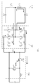
도 3은 본 발명의 일 실시예에 따른 무선 전력 송수신 장치의 일 예를 도시하는 회로도이고, 도 4 내지 도 9는 도 3에 도시된 무선 전력 송수신 장치의 동작을 설명하기 위한 참고 회로도이다.FIG. 3 is a circuit diagram showing an example of a wireless power transceiver according to an embodiment of the present invention, and FIGS. 4 to 9 are reference circuit diagrams for explaining the operation of the wireless power transceiver shown in FIG.
도 3을 참조하면, 무선 전력 송수신 장치(100)는 공진기(110), 브리지 회로부(120) 및 양방향 컨버터(130)를 포함한다.Referring to FIG. 3, a
공진기(110)는 복수의 공진 회로를 포함할 수 있다. The
도시된 예에서 공진기(110)는 제1 커패시터(C1)와 제1 인덕터(L1)로 구성되는 제1 공진회로와, 제2 커패시터(C2)와 제2 인덕터(L2)로 구성되는 제2 공진회로를 포함한다.In the illustrated example, the
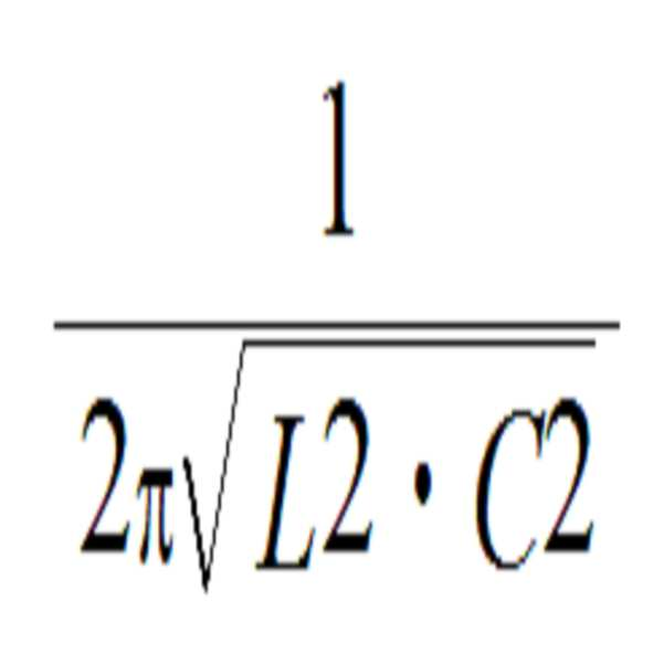
제1 공진 회로(C1, L1)와 제2 공진 회로(C2, L2)는 서로 다른 공진 특성을 가질 수 있다. 예를 들어, 제1 공진 회로(C1, L1)는 제1 공진 주파수를 가질 수 있고, 제2 공진 회로(C2, L2)는 제1 공진 주파수보다 낮은 제2 공진 주파수를 가질 수 있다.The first resonant circuit (C1, L1) and the second resonant circuit (C2, L2) can have different resonance characteristics. For example, the first resonant circuit (C1, L1) may have a first resonant frequency, and the second resonant circuit (C2, L2) may have a second resonant frequency lower than the first resonant frequency.
제1 주파수는 A4WP(Alliance for Wireless Power) 표준 주파수이고, 제2 주파수는 WPC(Wireless Power Consortium) 표준 주파수 또는 PMA(Power Matters Alliance) 표준 주파수일 수 있다. 이 경우, 제1 공진 주파수(
제1 공진 회로(C1, L1)와 제2 공진 회로(C2, L2)는 공통 단(common end)을 가질 수 있다. 도시된 예에서, 제1 공진 회로(C1, L1)와 제2 공진 회로(C2, L2)는 스위치 Q3 및 스위치 Q4에 연결되는 공통단을 가지고 있다.The first resonant circuit (C1, L1) and the second resonant circuit (C2, L2) may have a common end. In the illustrated example, the first resonant circuit (C1, L1) and the second resonant circuit (C2, L2) have a common terminal connected to switch Q3 and switch Q4.
브리지 회로부(120)는 복수의 브리지 회로를 포함할 수 있다.The
본 발명에서 브리지 회로는 2개의 스위치로 구성되며, 제1 공진회로 또는 제2 공진호로의 일 단에 연결되는 회로를 지칭한다. 따라서, 도 3에 도시된 예에서, 브리지 회로부(120)는 제1 스위치(Q1)와 제2 스위치(Q2)로 구성되는 제1 브리지 회로와, 제3 스위치(Q3)와 제4 스위치(Q4)로 구성되는 제2 브리지 회로, 및 제5 스위치(Q5)와 제6 스위치(Q6)로 구성되는 제3 브리지 회로를 포함한다.In the present invention, the bridge circuit is composed of two switches, and refers to a circuit connected to one end of the first resonant circuit or the second resonant circuit. 3, the
구체적으로, 제1 공진 회로(C1, L1)의 일단은 제1 브리지 회로(Q1, Q2)에 연결되고, 공통 단은 제2 브리지 회로(Q3, Q4)에 연결된다. 제2 공진 회로(C2, L2)의 일단은 제3 브리지 회로(Q5, Q6)에 연결된다.Specifically, one end of the first resonant circuit (C1, L1) is connected to the first bridge circuit (Q1, Q2), and a common end is connected to the second bridge circuit (Q3, Q4). One end of the second resonant circuit (C2, L2) is connected to the third bridge circuit (Q5, Q6).
브리지 회로부(120)는 복수의 브리지 회로의 동작에 따라, 정류기로서 동작하거나 인버터로서 동작할 수 있다. The
예를 들어, 제1 공진 회로(C1, L1)가 동작할 때, 제1 브리지 회로(Q1, Q2) 및 제2 브리지 회로(Q3, Q4)는 정류기 또는 인버터로서 동작할 수 있다. 한편, 제2 공진 회로(C2, L2)가 동작할 때, 제2 브리지 회로(Q3, Q4) 및 상기 제3 브리지 회로(Q5, Q6)는 정류기 또는 인버터로서 동작할 수 있다.For example, when the first resonant circuit (C1, L1) operates, the first bridge circuit (Q1, Q2) and the second bridge circuit (Q3, Q4) can operate as a rectifier or an inverter. On the other hand, when the second resonant circuit (C2, L2) operates, the second bridge circuit (Q3, Q4) and the third bridge circuit (Q5, Q6) can operate as a rectifier or an inverter.
양방향 컨버터(130)는 전력 수신 모드에서는 브리지 회로부(120)를 통하여 제공된 제1 전압을 감압하여 부하에 제공할 수 있다. 한편, 전력 송신 모드에서는 양방향 컨버터(130)는 부하에서 제공된 제2 전압을 승압하여 브리지 회로부(120)에 제공할 수 있다.The
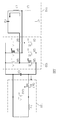
무선 전력 송수신 장치(100)는 링크 커패시터(Cl)를 포함할 수 있으며, 링크 커패시터(Cl)는 브리지 회로부(120) 및 양방향 컨버터(130)에 연결될 수 있다. The
링크 커패시터(Cl)는 전력 수신 모드에서는 축전된 전하를 양방향 컨버터(130), 즉, 부하에 제공하고, 전력 송신 모드에서는 축전된 전하를 브리지 회로부(120)에 제공할 수 있다.The link capacitor Cl may provide the charge stored in the power reception mode to the
양방향 컨버터(130)는 제1 컨버터 스위치(Qc1), 제2 컨버터 스위치(Qc2) 및 컨버터 인덕터(Lc)를 포함할 수 있다.The
제1 컨버터 스위치(Qc1)의 일단은 링크 커패시터(Cl)의 일단에, 제1 컨버터 스위치(Qc1)의 타단은 제2 컨버터 스위치(Qc2)의 일단 및 컨버터 인덕터(Lc)의 일단에 연결될 수 있다.One end of the first converter switch Qc1 may be connected to one end of the link capacitor Cl and the other end of the first converter switch Qc1 may be connected to one end of the second converter switch Qc2 and one end of the converter inductor Lc .
제2 컨버터 스위치(Qc2)의 일단은 제1 컨버터 스위치(Qc1)의 타단 및 컨버터 인덕터(Lc)의 일단에 연결될 있다. 제2 컨버터 스위치(Qc2)의 타단은 링크 커패시터(Cl)의 타단에 연결될 수 있다.One end of the second converter switch Qc2 is connected to the other end of the first converter switch Qc1 and one end of the converter inductor Lc. The other end of the second converter switch Qc2 may be connected to the other end of the link capacitor Cl.
컨버터 인덕터(Lc)의 일단은 제1 컨버터 스위치(Qc1)의 타단 및 제2 컨버터 스위치(Qc2)의 일단에 연결되고, 컨버터 인덕터(Lc)의 타단은 부하의 일단에 연결될 수 있다.
One end of the converter inductor Lc may be connected to the other end of the first converter switch Qc1 and one end of the second converter switch Qc2 and the other end of the converter inductor Lc may be connected to one end of the load.
이하, 도 4 내지 도 9를 참조하여, 상기 무선 전력 송수신 장치(100)의 각 모드에서의 동작에 대하여 설명한다.
Hereinafter, the operation in each mode of the wireless power transmitting /
도 4 및 도 5는 도 3에 도시된 무선 전력 송수신 장치의 제1 공진 회로(C1, L1)를 이용한 전력 수신 동작을 설명하는 참고 회로도이다.Figs. 4 and 5 are reference circuit diagrams illustrating a power receiving operation using the first resonant circuits C1 and L1 of the wireless power transmitting / receiving apparatus shown in Fig. 3. Fig.
제1 공진 회로(C1, L1)는 전력 송신 장치의 공진 회로에 자기적으로 결합하여, 교류 입력을 제공받을 수 있다.The first resonant circuit (C1, L1) may be magnetically coupled to the resonant circuit of the power transmitting device to receive the AC input.
교류 입력의 일 극성에서는, 도 4에 도시된 바와 같이, 제1 브리지 회로(Q1, Q2)의 제1 스위치(Q1)와 제2 브리지 회로(Q3, Q4)의 제4 스위치(Q4)를 통하여, 링크 커패시터(Cl)에 전하가 축전될 수 있다.In one polarity of the AC input, the first switch Q1 of the first bridge circuits Q1 and Q2 and the fourth switch Q4 of the second bridge circuits Q3 and Q4, as shown in Fig. 4, , Charge can be stored in the link capacitor Cl.
한편, 교류 입력의 다른 극성에서는, 도 5에 도시된 바와 같이, 제1 브리지 회로(Q1, Q2)의 제2 스위치(Q2)와 제2 브리지 회로(Q3, Q4)의 제3 스위치(Q3)를 통하여, 링크 커패시터(Cl)에 전하가 축전될 수 있다.5, the second switch Q2 of the first bridge circuits Q1 and Q2 and the third switch Q3 of the second bridge circuits Q3 and Q4 are turned on, A charge can be stored in the link capacitor Cl.
즉, 도 4 및 도 5에 도시된 바와 같이, 제1 브리지 회로(Q1, Q2) 및 제2 브리지 회로(Q3, Q4)는 정류 회로로서 동작할 수 있다.4 and 5, the first bridge circuits Q1 and Q2 and the second bridge circuits Q3 and Q4 can operate as a rectifying circuit.
한편, 양방향 컨버터(130)는 제1 컨버터 스위치(Qc1)에 대한 스위칭 제어에 따라, 링크 커패시터(Cl)의 전압을 가변하여 부하에 제공할 수 있다. 예를 들어, 제1 컨버터 스위치(Qc1)는 펄스 폭 변압 제어에 따라 스위칭 동작하여, 링크 커패시터(Cl)의 전압을 감압하여 부하에 제공할 수 있다. 이때, 제2 컨버터 스위치(Qc2)는 스위칭 제어되지 않을 수 있으며, 이러한 경우 기생 다이오드를 통한 경로를 통하여 전류가 흐를 수 있다. 한편, 기생 다이오드로 인한 경로가 존재하지 않는 경우라면, 제2 컨버터 스위치(Qc2)는 ON 상태로 설정될 수 있다.
On the other hand, the
도 6은 도 3에 도시된 무선 전력 송수신 장치의 제1 공진 회로를 이용한 전력 송신 동작을 설명하는 참고 회로도이다.FIG. 6 is a reference circuit diagram illustrating a power transmission operation using the first resonant circuit of the wireless power transmitting / receiving device shown in FIG. 3. FIG.
제1 공진 회로(C1, L1)는 전력 수신 장치의 공진 회로에 자기적으로 결합하여, 교류 전원을 제공할 수 있다.The first resonant circuits (C1, L1) are magnetically coupled to the resonant circuit of the power receiving device, and can provide AC power.
이를 위하여, 양방향 컨버터(130)는 부하의 전원을 승압하여 링크 커패시터(Cl)에 제공할 수 있다. 예를 들어, 양방향 컨버터(130)의 제2 컨버터 스위치(Qc2)에 대한 스위칭 제어-예를 들어, 펄스 폭 변조 제어-에 의하여, 부하의 전원은 컨버터 인덕터(Lc)에 충전 및 방전됨으로써 승압될 수 있다. 한편, 이때 제1 컨버터 스위치(Qc1)는 스위칭 제어되지 않을 수 있으며, 이러한 경우 기생 다이오드를 통한 경로를 통하여 전류가 흐를 수 있다. 한편, 기생 다이오드로 인한 경로가 존재하지 않는 경우라면, 제1 컨버터 스위치(Qc2)는 ON 상태로 설정될 수 있다.To this end,
브리지 회로부(120)는 링크 커패시터(Cl)에 저장된 직류 전원을 이용하여 교류 전원을 생성하여 제1 공진 회로(C1, L1)에 제공할 수 있다.The
일 예로, 브리지 회로부(120)는 제1 스위치(Q1)와 제4 스위치(Q4)의 교번적인 스위칭 동작에 따라 교류 전원을 생성할 수 있다. 이러한 예에서는 제3 스위치(Q3)는 ON 상태일 수 있다.For example, the
이 외에도 브리지 회로부(120)는 다양한 방식으로 동작할 수도 있다. In addition, the
예를 들어, 제4 스위치(Q4)를 ON 상태로 설정하여 접지화 시키고, 제1 스위치(Q1)와 제2 스위치(Q2)의 교번적인 스위칭 동작에 따라 교류 전원을 생성할 수 있다.For example, the fourth switch Q4 may be set to the ON state so as to be grounded, and the AC power supply may be generated in accordance with the alternate switching operation of the first switch Q1 and the second switch Q2.
다른 예를 들어, 제2 스위치(Q2)를 ON 상태로 설정하여 접지화 시키고, 제3 스위치(Q3)와 제4 스위치(Q4)의 교번적인 스위칭 동작에 따라 교류 전원을 생성할 수 있다.For another example, the second switch Q2 may be set to the ON state to ground, and the AC power supply may be generated according to the alternate switching operation of the third switch Q3 and the fourth switch Q4.
이와 같이, 전력 송신 모드에서, 양방향 컨버터(130)는 부스트 컨버터로서 동작하고, 브리지 회로부(120)는 인버터로서 동작함을 알 수 있다.
Thus, in the power transmission mode, it can be seen that
도 7 및 도 8은 도 3에 도시된 무선 전력 송수신 장치의 제2 공진 회로를 이용한 전력 수신 동작을 설명하는 참고 회로도이다.FIGS. 7 and 8 are reference circuit diagrams illustrating a power receiving operation using the second resonant circuit of the wireless power transmitting / receiving apparatus shown in FIG.
제2 공진 회로(C2, L2)는 전력 송신 장치의 공진 회로에 자기적으로 결합하여, 교류 입력을 제공받을 수 있다.The second resonant circuit (C2, L2) may be magnetically coupled to the resonant circuit of the power transmitting device to receive the AC input.
교류 입력의 일 극성에서는, 도 7에 도시된 바와 같이, 제2 브리지 회로(Q3, Q4)의 제3 스위치(Q3)와 제3 브리지 회로(Q5, Q6)의 제6 스위치(Q6)를 통하여, 링크 커패시터(Cl)에 전하가 축전될 수 있다.7, the third switch Q3 of the second bridge circuits Q3 and Q4 and the sixth switch Q6 of the third bridge circuits Q5 and Q6 are turned on , Charge can be stored in the link capacitor Cl.
한편, 교류 입력의 다른 극성에서는, 도 8에 도시된 바와 같이, 제2 브리지 회로(Q3, Q4)의 제4 스위치(Q4)와 제3 브리지 회로(Q5, Q6)의 제5 스위치(Q5)를 통하여, 링크 커패시터(Cl)에 전하가 축전될 수 있다.8, the fourth switch Q4 of the second bridge circuits Q3 and Q4 and the fifth switch Q5 of the third bridge circuits Q5 and Q6 are turned on, A charge can be stored in the link capacitor Cl.
즉, 도 7 및 도 8에 도시된 바와 같이, 제2 브리지 회로(Q3, Q4) 및 제3 브리지 회로(Q5, Q6)는 정류 회로로서 동작할 수 있다.That is, as shown in Figs. 7 and 8, the second bridge circuits Q3 and Q4 and the third bridge circuits Q5 and Q6 can operate as a rectifying circuit.
양방향 컨버터(130)는 제1 컨버터 스위치(Qc1)에 대한 스위칭 제어에 따라, 링크 커패시터(Cl)의 전압을 가변하여 부하에 제공할 수 있다. 예를 들어, 제1 컨버터 스위치(Qc1)는 펄스 폭 변압 제어에 따라 스위칭 동작하여, 링크 커패시터(Cl)의 전압을 감압하여 부하에 제공할 수 있다. 이때, 제2 컨버터 스위치(Qc2)는 스위칭 제어되지 않을 수 있으며, 이러한 경우 기생 다이오드를 통한 경로를 통하여 전류가 흐를 수 있다. 한편, 기생 다이오드로 인한 경로가 존재하지 않는 경우라면, 제2 컨버터 스위치(Qc2)는 ON 상태로 설정될 수 있다.
The
도 9는 도 3에 도시된 무선 전력 송수신 장치의 제2 공진 회로를 이용한 전력 송신 동작을 설명하는 참고 회로도이다. 9 is a reference circuit diagram illustrating a power transmission operation using the second resonant circuit of the wireless power transmitting / receiving device shown in FIG.
제2 공진 회로(C2, L2)는 전력 수신 장치의 공진 회로에 자기적으로 결합하여, 교류 전원을 제공할 수 있다.The second resonant circuits (C2, L2) can be magnetically coupled to the resonant circuit of the power receiving device to provide AC power.
이를 위하여, 양방향 컨버터(130)는 부하의 전원을 승압하여 링크 커패시터(Cl)에 제공할 수 있다. 예를 들어, 양방향 컨버터(130)의 제2 컨버터 스위치(Qc2)에 대한 스위칭 제어-예를 들어, 펄스 폭 변조 제어-에 의하여, 부하의 전원은 컨버터 인덕터(Lc)에 충전 및 방전됨으로써 승압될 수 있다. 한편, 이때 제1 컨버터 스위치(Qc1)는 스위칭 제어되지 않을 수 있으며, 이러한 경우 기생 다이오드를 통한 경로를 통하여 전류가 흐를 수 있다. 한편, 기생 다이오드로 인한 경로가 존재하지 않는 경우라면, 제1 컨버터 스위치(Qc2)는 ON 상태로 설정될 수 있다.To this end,
브리지 회로부(120)는 링크 커패시터(Cl)에 저장된 직류 전원을 이용하여 교류 전원을 생성하여 제2 공진 회로(C2, L2)에 제공할 수 있다.The
일 예로, 브리지 회로부(120)는 제3 스위치(Q3)와 제6 스위치(Q6)의 교번적인 스위칭 동작에 따라 교류 전원을 생성할 수 있다. 이러한 예에서는 제5 스위치(Q5)는 ON 상태일 수 있다.For example, the
이 외에도 브리지 회로부(120)는 다양한 방식으로 동작할 수도 있다. In addition, the
예를 들어, 제4 스위치(Q4)를 ON 상태로 설정하여 접지화 시키고, 제5 스위치(Q5)와 제6 스위치(Q6)의 교번적인 스위칭 동작에 따라 교류 전원을 생성할 수 있다.For example, the fourth switch Q4 may be set to the ON state to ground, and the AC power may be generated according to the alternate switching operation of the fifth switch Q5 and the sixth switch Q6.
다른 예를 들어, 제6 스위치(Q6)를 ON 상태로 설정하여 접지화 시키고, 제3 스위치(Q3)와 제4 스위치(Q4)의 교번적인 스위칭 동작에 따라 교류 전원을 생성할 수 있다.
As another example, the sixth switch Q6 may be set to the ON state to ground, and the AC power may be generated in accordance with the alternate switching operation of the third switch Q3 and the fourth switch Q4.
도 3 내지 도 9에서는 공통 단자를 포함하여 복수의 공진 회로를 가지는 예에 대하여 설명하였으나, 이는 예시적인 것이다.In Figs. 3 to 9, an example having a plurality of resonant circuits including a common terminal has been described, but this is merely an example.
즉, 도 3에서 공진기(110)는 제1 공진 회로(C1, L1)와 제2 공진 회로(C2, L2)로 구성되나, 이는 다양하게 변형실시 될 수 있다. 예를 들어, 제1 커패시터와 제1 인덕터로 구성되는 제1 공진 회로를, 제1 및 제2 커패시터(C1, C2)와 제1 및 제2 인덕터로 구성되는 제2 공진 회로를 이용할 수 도 있다.
3, the
한편, 공진기는 공통 단자 없이도 복수의 공진 회로를 포함할 수 있으며, 이러한 예에 대해서는 도 10 내지 도 16을 참조하여 설명한다.
On the other hand, the resonator may include a plurality of resonant circuits without a common terminal, and such an example will be described with reference to FIGS. 10 to 16. FIG.
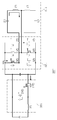
도 10은 본 발명의 일 실시예에 따른 무선 전력 송수신 장치의 다른 일 예를 도시하는 회로도이다.10 is a circuit diagram showing another example of a wireless power transceiver according to an embodiment of the present invention.
도 10을 참조하면, 공진기(111)는 제1 공진 회로와 제2 공진 회로를 포함할 수 있다.Referring to FIG. 10, the
제1 공진 회로는 제1 커패시터(C11)와 제1 인덕터(L11)로 구성되고, 제2 공진 회로는 제2 커패시터(C12)와 제2 인덕터(L12)로 구성될 수 있다. 제1 공진 회로는 제1 공진 주파수를 가지고, 제2 공진 회로는 상기 제1 공진 주파수보다 낮은 제2 공진 주파수를 가질 수 있다.The first resonant circuit may include a first capacitor C11 and a first inductor L11 and the second resonant circuit may include a second capacitor C12 and a second inductor L12. The first resonant circuit may have a first resonant frequency and the second resonant circuit may have a second resonant frequency that is lower than the first resonant frequency.
브리지 회로부(120)는 복수의 브리지 회로를 포함하고, 복수의 브리지 회로 중 적어도 일부는 제1 공진 회로와 연결되고, 복수의 브리지 회로 중 나머지 일부는 제2 공진 회로와 연결될 수 있다.The
도시된 예에서, 브리지 회로부(121)는 4개의 브리지 회로를 포함하며, 제1 브리지 회로(Q11, Q12) 및 제2 브리지 회로(Q13, Q14)는 제1 공진 회로에 연결되고, 제3 브리지 회로(Q15, Q16) 및 제4 브리지 회로(Q17, Q18)는 제2 공진 회로에 연결된다.In the illustrated example, the
브리지 회로부(121)는 전력 수신 모드에서는 정류기로서 동작하고, 전력 송신 모드에서는 인버터로서 동작함은 이미 설명한 바와 같다.It is already described that the
브리지 회로부(121)의 일단에는 링크 커패시터(Cl1)가 연결되며, 또한 양방향 컨버터(131)가 연결된다.A link capacitor Cl1 is connected to one end of the
링크 커패시터(Cl1)는 전력 수신 모드에서는 축전된 전하를 양방향 컨버터(131)측, 즉 부하에 제공하고, 전력 송신 모드에서는 축전된 전하를 브리지 회로부(121)에 제공할 수 있다.The link capacitor Cl1 can provide the stored charge to the
양방향 컨버터(131)는 전력 수신 모드에서는 브리지 회로부(121)를 통하여 제공된 제1 전압을 감압하여 부하로 제공할 수 있다. 한편, 전력 송신 모드에서는 부하에서 제공된 제2 전압을 승압하여 링크 커패시터(Cl1)에 제공할 수 있다.In the power receiving mode,
양방향 컨버터(130)는 제1 컨버터 스위치(Qc11), 제2 컨버터 스위치(Qc12) 및 컨버터 인덕터(Lc1)를 포함할 수 있다.The
제1 컨버터 스위치(Qc11)의 일단은 링크 커패시터(Cl1)의 일단에, 제1 컨버터 스위치(Qc11)의 타단은 제2 컨버터 스위치(Qc12)의 일단 및 컨버터 인덕터(Lc1)의 일단에 연결될 수 있다.One end of the first converter switch Qc11 may be connected to one end of the link capacitor Cl1 and the other end of the first converter switch Qc11 may be connected to one end of the second converter switch Qc12 and one end of the converter inductor Lc1 .
제2 컨버터 스위치(Qc12)의 일단은 제1 컨버터 스위치(Qc11)의 타단 및 컨버터 인덕터(Lc1)의 일단에 연결될 있다. 제2 컨버터 스위치(Qc21)의 타단은 링크 커패시터(Cl1)의 타단에 연결될 수 있다.One end of the second converter switch Qc12 is connected to the other end of the first converter switch Qc11 and one end of the converter inductor Lc1. The other end of the second converter switch Qc21 may be connected to the other end of the link capacitor Cl1.
컨버터 인덕터(Lc1)의 일단은 제1 컨버터 스위치(Qc11)의 타단 및 제2 컨버터 스위치(Qc12)의 일단에 연결되고, 컨버터 인덕터(Lc1)의 타단은 부하의 일단에 연결될 수 있다.
One end of the converter inductor Lc1 may be connected to the other end of the first converter switch Qc11 and one end of the second converter switch Qc12 and the other end of the converter inductor Lc1 may be connected to one end of the load.
이하, 도 11 내지 도 16를 참조하여, 상기 무선 전력 송수신 장치(101)의 각 모드에서의 동작에 대하여 설명한다.Hereinafter, operations in the respective modes of the wireless power transmission /
도 11 및 도 12는 도 10에 도시된 무선 전력 송수신 장치의 제1 공진 회로(C11, L11)를 이용한 전력 수신 동작을 설명하는 참고 회로도이다.11 and 12 are reference circuit diagrams for explaining a power receiving operation using the first resonant circuits C11 and L11 of the wireless power transmitting / receiving apparatus shown in FIG.
제1 공진 회로(C11, L11)는 전력 송신 장치의 공진 회로에 자기적으로 결합하여, 교류 입력을 제공받을 수 있다.The first resonant circuits C11 and L11 may be magnetically coupled to the resonant circuit of the power transmitting device to receive the AC input.
교류 입력의 일 극성에서는, 도 11에 도시된 바와 같이, 제1 브리지 회로(Q11, Q12)의 제1 스위치(Q11)와 제2 브리지 회로(Q13, Q14)의 제4 스위치(Q14)를 통하여, 링크 커패시터(Cl)에 전하가 축전될 수 있다.11, the first switch Q11 of the first bridge circuits Q11 and Q12 and the fourth switch Q14 of the second bridge circuits Q13 and Q14 are turned on , Charge can be stored in the link capacitor Cl.
한편, 교류 입력의 다른 극성에서는, 도 12에 도시된 바와 같이, 제1 브리지 회로(Q11, Q12)의 제2 스위치(Q12)와 제2 브리지 회로(Q13, Q14)의 제3 스위치(Q13)를 통하여, 링크 커패시터(Cl1)에 전하가 축전될 수 있다.12, the second switch Q12 of the first bridge circuits Q11 and Q12 and the third switch Q13 of the second bridge circuits Q13 and Q14 are turned on, The charge can be stored in the link capacitor Cl1.
즉, 제1 브리지 회로(Q1, Q2) 및 제2 브리지 회로(Q3, Q4)는 정류 회로로서 동작할 수 있다.That is, the first bridge circuits (Q1, Q2) and the second bridge circuits (Q3, Q4) can operate as a rectifying circuit.
양방향 컨버터(131)가 제1 컨버터 스위치(Qc11)에 대한 스위칭 제어에 따라, 링크 커패시터(Cl1)의 전압을 감압하여 부하에 제공하는 것은 상술한 내용으로부터 이해할 수 있다.
It is understood from the above description that the
도 13은 도 10에 도시된 무선 전력 송수신 장치의 제1 공진 회로를 이용한 전력 송신 동작을 설명하는 참고 회로도이다.13 is a reference circuit diagram for explaining a power transmission operation using the first resonant circuit of the wireless power transmitting / receiving apparatus shown in Fig.
제1 공진 회로(C11, L11)는 전력 수신 장치의 공진 회로에 자기적으로 결합하여, 교류 전원을 제공할 수 있다.The first resonant circuits C11 and L11 may be magnetically coupled to the resonant circuit of the power receiving device to provide AC power.
이를 위하여, 양방향 컨버터(131)는 부하의 전원을 승압하여 링크 커패시터(Cl1)에 제공할 수 있다. 예를 들어, 양방향 컨버터(131)의 제2 컨버터 스위치(Qc12)에 대한 스위칭 제어-예를 들어, 펄스 폭 변조 제어-에 의하여, 부하의 전원은 컨버터 인덕터(Lc)에 충전 및 방전됨으로써 승압될 수 있다. For this purpose, the
브리지 회로부(121)는 링크 커패시터(Cl1)에 저장된 직류 전원을 이용하여 교류 전원을 생성하여 제1 공진 회로(C11, L11)에 제공할 수 있다.The
일 예로, 브리지 회로부(120)는 제1 스위치(Q11)와 제4 스위치(Q14)의 교번적인 스위칭 동작에 따라 교류 전원을 생성할 수 있다. 이러한 예에서는 제3 스위치(Q13)는 ON 상태일 수 있다.For example, the
이 외에도 브리지 회로부(120)는 다양한 방식으로 동작할 수도 있다.In addition, the
예를 들어, 제4 스위치(Q14)를 ON 상태로 설정하여 접지화 시키고, 제1 스위치(Q11)와 제2 스위치(Q12)의 교번적인 스위칭 동작에 따라 교류 전원을 생성할 수 있다.For example, the fourth switch Q14 may be set to the ON state to ground, and the alternating current power may be generated in accordance with the alternate switching operation of the first switch Q11 and the second switch Q12.
다른 예를 들어, 제2 스위치(Q12)를 ON 상태로 설정하여 접지화 시키고, 제3 스위치(Q13)와 제4 스위치(Q14)의 교번적인 스위칭 동작에 따라 교류 전원을 생성할 수 있다.For example, the second switch Q12 may be set to the ON state to ground, and the AC power may be generated in accordance with the alternate switching operation of the third switch Q13 and the fourth switch Q14.
이와 같이, 전력 송신 모드에서, 양방향 컨버터(131)는 부스트 컨버터로서 동작하고, 브리지 회로부(121)는 인버터로서 동작한다.
Thus, in the power transmission mode,
도 14 및 도 15는 도 10에 도시된 무선 전력 송수신 장치의 제2 공진 회로를 이용한 전력 수신 동작을 설명하는 참고 회로도이다.Figs. 14 and 15 are reference circuit diagrams illustrating a power receiving operation using the second resonant circuit of the wireless power transmitting / receiving device shown in Fig. 10. Fig.
제2 공진 회로(C12, L12)는 전력 송신 장치의 공진 회로에 자기적으로 결합하여, 교류 입력을 제공받을 수 있다.The second resonant circuits C12 and L12 may be magnetically coupled to the resonant circuit of the power transmitting device to receive the AC input.
교류 입력의 일 극성에서는, 도 14에 도시된 바와 같이, 제2 브리지 회로(Q13, Q14)의 제3 스위치(Q13)와 제3 브리지 회로(Q15, Q16)의 제6 스위치(Q16)를 통하여, 링크 커패시터(Cl1)에 전하가 축전될 수 있다.14, the third switch Q13 of the second bridge circuits Q13 and Q14 and the sixth switch Q16 of the third bridge circuits Q15 and Q16 are turned on , Charge can be stored in the link capacitor Cl1.
한편, 교류 입력의 다른 극성에서는, 도 15에 도시된 바와 같이, 제2 브리지 회로(Q13, Q14)의 제4 스위치(Q14)와 제3 브리지 회로(Q15, Q16)의 제5 스위치(Q15)를 통하여, 링크 커패시터(Cl1)에 전하가 축전될 수 있다.15, the fourth switch Q14 of the second bridge circuits Q13 and Q14 and the fifth switch Q15 of the third bridge circuits Q15 and Q16 are turned on, The charge can be stored in the link capacitor Cl1.
즉, 도 14 및 도 5에 도시된 바와 같이, 제2 브리지 회로(Q13, Q14) 및 제3 브리지 회로(Q15, Q61)는 정류 회로로서 동작할 수 있다.That is, as shown in Figs. 14 and 5, the second bridge circuits Q13 and Q14 and the third bridge circuits Q15 and Q61 can operate as a rectifying circuit.
양방향 컨버터(131)는 제1 컨버터 스위치(Qc11)에 대한 스위칭 제어에 따라, 링크 커패시터(Cl1)의 전압을 가변하여 부하에 제공할 수 있음은 상술한 바와 같다.
As described above, the
도 16은 도 10에 도시된 무선 전력 송수신 장치의 제2 공진 회로를 이용한 전력 송신 동작을 설명하는 참고 회로도이다. 16 is a reference circuit diagram for explaining a power transmission operation using the second resonant circuit of the wireless power transmitting / receiving device shown in Fig.
제2 공진 회로(C12, L12)는 전력 수신 장치의 공진 회로에 자기적으로 결합하여, 교류 전원을 제공할 수 있다.The second resonant circuits (C12, L12) can be magnetically coupled to the resonant circuit of the power receiving device to provide AC power.
양방향 컨버터(131)의 제2 컨버터 스위치(Qc12)에 대한 스위칭 제어-예를 들어, 펄스 폭 변조 제어-에 의하여, 부하의 전원은 컨버터 인덕터(Lc)의 충전 및 방전에 의하여 승압되어 링크 커패시터(Cl1)에 제공될 수 있다. The power of the load is stepped up by the charging and discharging of the converter inductor Lc by the switching control of the
브리지 회로부(121)는 링크 커패시터(Cl1)에 저장된 직류 전원을 이용하여 교류 전원을 생성하여 제2 공진 회로(C12, L12)에 제공할 수 있다.The
일 예로, 브리지 회로부(121)는 제5 스위치(Q5)와 제8 스위치(Q18)의 교번적인 스위칭 동작에 따라 교류 전원을 생성할 수 있다. 이러한 예에서는 제7 스위치(Q17)는 ON 상태일 수 있다.For example, the
이 외에도 브리지 회로부(120)는 다양한 방식으로 동작할 수도 있다. In addition, the
예를 들어, 제6 스위치(Q16)를 ON 상태로 설정하여 접지화 시키고, 제7 스위치(Q17)와 제8 스위치(Q18)의 교번적인 스위칭 동작에 따라 교류 전원을 생성할 수 있다.For example, the sixth switch Q16 may be set to the ON state to ground, and the AC power supply may be generated according to the alternate switching operation of the seventh switch Q17 and the eighth switch Q18.
다른 예를 들어, 제8 스위치(Q18)를 ON 상태로 설정하여 접지화 시키고, 제5 스위치(Q15)와 제6 스위치(Q16)의 교번적인 스위칭 동작에 따라 교류 전원을 생성할 수 있다.
For example, the eighth switch Q18 may be set to the ON state to be grounded, and the AC power supply may be generated according to the alternate switching operation of the fifth switch Q15 and the sixth switch Q16.
이상에서 본 발명이 구체적인 구성요소 등과 같은 특정 사항들과 한정된 실시예 및 도면에 의해 설명되었으나, 이는 본 발명의 보다 전반적인 이해를 돕기 위해서 제공된 것일 뿐, 본 발명이 상기 실시예들에 한정되는 것은 아니며, 본 발명이 속하는 기술분야에서 통상적인 지식을 가진 자라면 이러한 기재로부터 다양한 수정 및 변형을 꾀할 수 있다.
While the present invention has been particularly shown and described with reference to exemplary embodiments thereof, it is to be understood that the invention is not limited to the disclosed exemplary embodiments, but, on the contrary, Those skilled in the art will appreciate that various modifications, additions and substitutions are possible, without departing from the scope and spirit of the invention as disclosed in the accompanying claims.
따라서, 본 발명의 사상은 상기 설명된 실시예에 국한되어 정해져서는 아니 되며, 후술하는 특허청구범위뿐만 아니라 이 특허청구범위와 균등하게 또는 등가적으로 변형된 모든 것들은 본 발명의 사상의 범주에 속한다고 할 것이다.
Therefore, the spirit of the present invention should not be construed as being limited to the above-described embodiments, and all of the equivalents or equivalents of the claims, as well as the following claims, I will say.
10 : 전자 기기
20 : 무선 전력 송신 장치
100 : 무선 전력 송수신 장치
110 : 공진기
120 : 브리지 회로부
130 : 양방향 컨버터10: Electronic device
20: Wireless power transmitter
100: wireless power transmitter / receiver
110: Resonator
120: bridge circuit part
130: Bi-directional converter
Claims (15)
상기 공진기에 연결되고, 전력 수신 모드에서는 정류기로 동작하고 전력 송신 모드에서는 인버터로 동작하는 브리지 회로부; 및
상기 브리지 회로부에 연결되고, 상기 전력 수신 모드에서는 감압 동작하고 상기 전력 송신 모드에서는 승압 동작하는 양방향 컨버터;
를 포함하는 무선 전력 송수신 장치.
A resonator magnetically coupled to the wireless power transmission device or the wireless power reception device;
A bridge circuit part connected to the resonator and operating as a rectifier in a power reception mode and as an inverter in a power transmission mode; And
A bidirectional converter that is connected to the bridge circuit and operates in a reduced voltage in the power receiving mode and in a power transmitting mode;
Gt; transmitting / receiving < / RTI >
제1 공진 주파수를 가지는 제1 공진 회로; 및
상기 제1 공진 주파수보다 낮은 제2 공진 주파수를 가지는 제2 공진 회로; 를 포함하고,
상기 제1 공진 회로 및 상기 제2 공진 회로는 하나의 공통 단(common end)을 가지는 무선 전력 송수신 장치.
The resonator according to claim 1, wherein the resonator
A first resonant circuit having a first resonant frequency; And
A second resonant circuit having a second resonant frequency lower than the first resonant frequency; Lt; / RTI >
Wherein the first resonant circuit and the second resonant circuit have one common end.
제1 브리지 회로, 제2 브리지 회로 및 제3 브리지 회로를 포함하고,
상기 제1 공진 회로가 동작할 때, 상기 제1 브리지 회로 및 상기 제2 브리지 회로는 정류기 또는 인버터로서 동작하고,
상기 제2 공진 회로가 동작할 때, 상기 제2 브리지 회로 및 상기 제3 브리지 회로는 정류기 또는 인버터로서 동작하는 무선 전력 송수신 장치.
3. The semiconductor device according to claim 2, wherein the bridge circuit portion
A first bridge circuit, a second bridge circuit and a third bridge circuit,
When the first resonant circuit operates, the first bridge circuit and the second bridge circuit operate as a rectifier or an inverter,
And the second bridge circuit and the third bridge circuit operate as a rectifier or an inverter when the second resonant circuit operates.
제1 브리지 회로, 제2 브리지 회로 및 제3 브리지 회로를 포함하고,
상기 제1 공진 회로의 일단은 상기 제1 브리지 회로에, 상기 공통 단은 제2 브리지 회로에, 상기 제2 공진 회로의 일단은 상기 제3 브리지 회로에 연결되는 무선 전력 송수신 장치.
3. The semiconductor device according to claim 2, wherein the bridge circuit portion
A first bridge circuit, a second bridge circuit and a third bridge circuit,
Wherein one end of the first resonant circuit is connected to the first bridge circuit, the common end to a second bridge circuit, and the other end of the second resonant circuit is connected to the third bridge circuit.
상기 전력 수신 모드에서는 상기 브리지 회로부를 통하여 제공된 제1 전압을 감압하여 부하에 제공하고, 상기 전력 송신 모드에서는 상기 부하에서 제공된 제2 전압을 승압하여 상기 브리지 회로부에 제공하는 무선 전력 송수신 장치.
The method of claim 1, wherein the bidirectional converter
Wherein the power receiving mode provides a reduced voltage to the load through the bridge circuit unit and provides the load to the bridge circuit unit by boosting the second voltage provided in the load in the power transmission mode.
상기 브리지 회로부 및 상기 양방향 컨버터에 연결되는 링크 커패시터;
를 더 포함하고,
상기 링크 커패시터는
상기 전력 수신 모드에서는 축전된 전하를 상기 양방향 컨버터에 제공하고, 상기 전력 송신 모드에서는 축전된 전하를 상기 브리지 회로부에 제공하는 무선 전력 송수신 장치.
The apparatus of claim 1, wherein the wireless power transceiver
A link capacitor connected to the bridge circuit unit and the bidirectional converter;
Further comprising:
The link capacitor
And provides the stored charge to the bidirectional converter in the power receiving mode and provides the stored charge to the bridge circuit in the power transmitting mode.
일단이 상기 링크 커패시터의 일단에 연결되는 제1 컨버터 스위치;
일단이 상기 제1 컨버터 스위치의 타단에 연결되고, 타단이 상기 링크 커패시터의 타단에 연결되는 제2 컨버터 스위치; 및
일단이 상기 제1 컨버터 스위치의 타단과 상기 제2 컨버터 스위치의 일단에 연결되는 인덕터;
를 포함하는 무선 전력 송수신 장치.
7. The method of claim 6, wherein the bidirectional converter
A first converter switch having one end connected to one end of the link capacitor;
A second converter switch having one end connected to the other end of the first converter switch and the other end connected to the other end of the link capacitor; And
An inductor whose one end is connected to the other end of the first converter switch and one end of the second converter switch;
Gt; transmitting / receiving < / RTI >
상기 전력 수신 모드에서,
상기 제1 컨버터 스위치는 펄스 폭 변압 제어에 따라 스위칭 동작하고,
상기 제2 컨버터 스위치는 스위칭 제어되지 않는 무선 전력 송수신 장치.
8. The method of claim 7,
In the power receiving mode,
Wherein the first converter switch performs a switching operation in accordance with the pulse width change control,
And the second converter switch is not switched-controlled.
상기 전력 송신 모드에서,
상기 제1 컨버터 스위치는 스위칭 제어되지 않고,
상기 제2 컨버터 스위치는 펄스 폭 변압 제어에 따라 스위칭 동작하는 무선 전력 송수신 장치.
8. The method of claim 7,
In the power transmission mode,
The first converter switch is not switched,
And the second converter switch performs switching operation according to pulse width modulation control.
상기 제1 공진 주파수보다 낮은 제2 공진 주파수를 가지는 제2 공진 회로;
복수의 브리지 회로를 포함하고, 복수의 브리지 회로 중 적어도 일부는 상기 제1 공진 회로와 연결되고, 복수의 브리지 회로 중 나머지 일부는 상기 제2 공진 회로와 연결되는 브리지 회로부; 및
상기 브리지 회로부에 연결되고, 전력 수신 모드에서는 상기 브리지 회로부를 통하여 제공된 제1 전압을 감압하고, 전력 송신 모드에서는 부하에서 제공된 제2 전압을 승압하는 양방향 컨버터;
를 포함하는 무선 전력 송수신 장치.
A first resonant circuit having a first resonant frequency;
A second resonant circuit having a second resonant frequency lower than the first resonant frequency;
A bridge circuit part including a plurality of bridge circuits, at least a part of the plurality of bridge circuits being connected to the first resonant circuit, and a remaining part of the plurality of bridge circuits being connected to the second resonant circuit; And
A bidirectional converter connected to the bridge circuit unit for reducing a first voltage provided through the bridge circuit unit in a power reception mode and for boosting a second voltage provided in a load in a power transmission mode;
Gt; transmitting / receiving < / RTI >
상기 전력 수신 모드에서는 정류기로서 동작하고, 상기 전력 송신 모드에서는 인버터로서 동작하는 무선 전력 송수신 장치.
11. The apparatus of claim 10, wherein the bridge circuit portion
And operates as a rectifier in the power receiving mode and as an inverter in the power transmitting mode.
상기 브리지 회로부 및 상기 양방향 컨버터에 연결되는 링크 커패시터;
를 더 포함하고,
상기 링크 커패시터는
상기 전력 수신 모드에서는 축전된 전하를 상기 양방향 컨버터에 제공하고, 상기 전력 송신 모드에서는 축전된 전하를 상기 브리지 회로부에 제공하는 무선 전력 송수신 장치.
11. The apparatus of claim 10, wherein the wireless power transceiver
A link capacitor connected to the bridge circuit unit and the bidirectional converter;
Further comprising:
The link capacitor
And provides the stored charge to the bidirectional converter in the power receiving mode and provides the stored charge to the bridge circuit in the power transmitting mode.
일단이 상기 링크 커패시터의 일단에 연결되는 제1 컨버터 스위치;
일단이 상기 제1 컨버터 스위치의 타단에 연결되고, 타단이 상기 링크 커패시터의 타단에 연결되는 제2 컨버터 스위치; 및
일단이 상기 제1 컨버터 스위치의 타단과 상기 제2 컨버터 스위치의 일단에 연결되는 인덕터;
를 포함하는 무선 전력 송수신 장치.
13. The method of claim 12, wherein the bidirectional converter
A first converter switch having one end connected to one end of the link capacitor;
A second converter switch having one end connected to the other end of the first converter switch and the other end connected to the other end of the link capacitor; And
An inductor whose one end is connected to the other end of the first converter switch and one end of the second converter switch;
Gt; transmitting / receiving < / RTI >
상기 전력 수신 모드에서,
상기 제1 컨버터 스위치는 펄스 폭 변압 제어에 따라 스위칭 동작하고,
상기 제2 컨버터 스위치는 스위칭 제어되지 않는 무선 전력 송수신 장치.
14. The method of claim 13,
In the power receiving mode,
Wherein the first converter switch performs a switching operation in accordance with the pulse width change control,
And the second converter switch is not switched-controlled.
상기 전력 송신 모드에서,
상기 제1 컨버터 스위치는 스위칭 제어되지 않고,
상기 제2 컨버터 스위치는 펄스 폭 변압 제어에 따라 스위칭 동작하는 무선 전력 송수신 장치.
14. The method of claim 13,
In the power transmission mode,
The first converter switch is not switched,
And the second converter switch performs switching operation according to pulse width modulation control.
Priority Applications (2)
| Application Number | Priority Date | Filing Date | Title |
|---|---|---|---|
| KR1020160009647A KR20170089350A (en) | 2016-01-26 | 2016-01-26 | Wirelessly power tranceiver |
| CN201610622158.1A CN106998102A (en) | 2016-01-26 | 2016-08-01 | Wireless power R-T unit |
Applications Claiming Priority (1)
| Application Number | Priority Date | Filing Date | Title |
|---|---|---|---|
| KR1020160009647A KR20170089350A (en) | 2016-01-26 | 2016-01-26 | Wirelessly power tranceiver |
Publications (1)
| Publication Number | Publication Date |
|---|---|
| KR20170089350A true KR20170089350A (en) | 2017-08-03 |
Family
ID=59430968
Family Applications (1)
| Application Number | Title | Priority Date | Filing Date |
|---|---|---|---|
| KR1020160009647A KR20170089350A (en) | 2016-01-26 | 2016-01-26 | Wirelessly power tranceiver |
Country Status (2)
| Country | Link |
|---|---|
| KR (1) | KR20170089350A (en) |
| CN (1) | CN106998102A (en) |
Cited By (1)
| Publication number | Priority date | Publication date | Assignee | Title |
|---|---|---|---|---|
| KR20190067018A (en) * | 2017-12-06 | 2019-06-14 | 삼성전기주식회사 | Apparatus for transmiting power wirelessly |
Family Cites Families (3)
| Publication number | Priority date | Publication date | Assignee | Title |
|---|---|---|---|---|
| JP5494838B2 (en) * | 2011-01-26 | 2014-05-21 | 株式会社村田製作所 | Power transmission system |
| US9748774B2 (en) * | 2012-09-07 | 2017-08-29 | Access Business Group International Llc | System and method for bidirectional wireless power transfer |
| EP3123592B1 (en) * | 2014-03-27 | 2019-08-21 | Schneider Electric IT Corporation | Bi-directional dc-dc converter |
-
2016
- 2016-01-26 KR KR1020160009647A patent/KR20170089350A/en not_active Application Discontinuation
- 2016-08-01 CN CN201610622158.1A patent/CN106998102A/en active Pending
Cited By (1)
| Publication number | Priority date | Publication date | Assignee | Title |
|---|---|---|---|---|
| KR20190067018A (en) * | 2017-12-06 | 2019-06-14 | 삼성전기주식회사 | Apparatus for transmiting power wirelessly |
Also Published As
| Publication number | Publication date |
|---|---|
| CN106998102A (en) | 2017-08-01 |
Similar Documents
| Publication | Publication Date | Title |
|---|---|---|
| US10193389B2 (en) | Multi-bridge topology | |
| US10284018B2 (en) | System, apparatus and method for adaptive tuning for wireless power transfer | |
| US9088307B2 (en) | Non-resonant and quasi-resonant system for wireless power transmission to multiple receivers | |
| CN106357011B (en) | Radio energy transmitter | |
| US10141769B2 (en) | Wireless power transfer system | |
| JP2018078795A (en) | Power-receiving device | |
| CN103580300A (en) | Receiver and method for executing operation of receiver | |
| EP2819273B1 (en) | Wireless power transmission device | |
| CN102035266A (en) | Wireless power feeder and wireless power transmission system | |
| KR101837121B1 (en) | Dual band Wireless Power Receiving Unit | |
| US10938244B2 (en) | Bidirectional wireless power transmission system | |
| JP5716877B2 (en) | Power transmission system | |
| US9577438B2 (en) | Wireless power system | |
| WO2013151123A1 (en) | Non-contact power transmitting apparatus and non-contact power transmitting system | |
| WO2015083578A1 (en) | Contactless power transmission device and electricity reception apparatus | |
| KR20170089350A (en) | Wirelessly power tranceiver | |
| JP2019161929A (en) | Wireless power transmission system and power reception device | |
| JP2019161937A (en) | Wireless power transmission system and power transmission device | |
| NL2022009B1 (en) | Multimodal charging of a load | |
| JP6133153B2 (en) | Electromagnetic field suppressor and wireless power transmission system using the same | |
| KR20170104883A (en) | A wireless power receiver and thereof operation method | |
| CN112753151A (en) | System for transmitting electric power to an electric load | |
| JP2021083140A (en) | Power reception device | |
| JP7071193B2 (en) | Power transmission device | |
| KR20160070539A (en) | Wireless Power Transfer System |
Legal Events
| Date | Code | Title | Description |
|---|---|---|---|
| N231 | Notification of change of applicant | ||
| E902 | Notification of reason for refusal | ||
| E601 | Decision to refuse application |