EP2464006A1 - Method for manufacturing an acoustic-wave resonator including a suspended membrane - Google Patents
Method for manufacturing an acoustic-wave resonator including a suspended membrane Download PDFInfo
- Publication number
- EP2464006A1 EP2464006A1 EP11191911A EP11191911A EP2464006A1 EP 2464006 A1 EP2464006 A1 EP 2464006A1 EP 11191911 A EP11191911 A EP 11191911A EP 11191911 A EP11191911 A EP 11191911A EP 2464006 A1 EP2464006 A1 EP 2464006A1
- Authority
- EP
- European Patent Office
- Prior art keywords
- manufacturing
- acoustic wave
- wave resonator
- resonator according
- bonding
- Prior art date
- Legal status (The legal status is an assumption and is not a legal conclusion. Google has not performed a legal analysis and makes no representation as to the accuracy of the status listed.)
- Granted
Links
- 238000004519 manufacturing process Methods 0.000 title claims description 42
- 239000012528 membrane Substances 0.000 title claims description 21
- 238000000034 method Methods 0.000 title abstract description 24
- 239000000758 substrate Substances 0.000 claims abstract description 54
- 239000000463 material Substances 0.000 claims abstract description 44
- 239000002086 nanomaterial Substances 0.000 claims abstract description 21
- 239000002245 particle Substances 0.000 claims abstract description 15
- 230000000977 initiatory effect Effects 0.000 claims abstract description 11
- 238000010438 heat treatment Methods 0.000 claims description 17
- 238000000151 deposition Methods 0.000 claims description 14
- 229910052710 silicon Inorganic materials 0.000 claims description 12
- 239000010703 silicon Substances 0.000 claims description 12
- 230000008021 deposition Effects 0.000 claims description 9
- 229910052751 metal Inorganic materials 0.000 claims description 9
- 239000002184 metal Substances 0.000 claims description 9
- 238000005498 polishing Methods 0.000 claims description 8
- 229910004298 SiO 2 Inorganic materials 0.000 claims description 4
- 238000004026 adhesive bonding Methods 0.000 claims description 4
- 238000005530 etching Methods 0.000 claims description 4
- 229930195733 hydrocarbon Natural products 0.000 claims description 4
- 150000002430 hydrocarbons Chemical group 0.000 claims description 4
- 238000002360 preparation method Methods 0.000 claims description 4
- VYPSYNLAJGMNEJ-UHFFFAOYSA-N silicon dioxide Inorganic materials O=[Si]=O VYPSYNLAJGMNEJ-UHFFFAOYSA-N 0.000 claims description 4
- 239000006227 byproduct Substances 0.000 claims description 3
- 238000005468 ion implantation Methods 0.000 claims description 3
- 238000001459 lithography Methods 0.000 claims description 3
- 239000010453 quartz Substances 0.000 claims description 3
- 238000011282 treatment Methods 0.000 claims description 3
- CBENFWSGALASAD-UHFFFAOYSA-N Ozone Chemical compound [O-][O+]=O CBENFWSGALASAD-UHFFFAOYSA-N 0.000 claims description 2
- 238000003486 chemical etching Methods 0.000 claims description 2
- 239000002131 composite material Substances 0.000 claims description 2
- 239000010432 diamond Substances 0.000 claims description 2
- 229910003460 diamond Inorganic materials 0.000 claims description 2
- 239000003989 dielectric material Substances 0.000 claims description 2
- 230000004927 fusion Effects 0.000 claims description 2
- 239000012263 liquid product Substances 0.000 claims description 2
- 229910052594 sapphire Inorganic materials 0.000 claims description 2
- 239000010980 sapphire Substances 0.000 claims description 2
- 239000012265 solid product Substances 0.000 claims description 2
- 239000010410 layer Substances 0.000 description 46
- 239000010409 thin film Substances 0.000 description 13
- XUIMIQQOPSSXEZ-UHFFFAOYSA-N Silicon Chemical compound [Si] XUIMIQQOPSSXEZ-UHFFFAOYSA-N 0.000 description 12
- 238000002513 implantation Methods 0.000 description 11
- 238000005516 engineering process Methods 0.000 description 10
- 238000012546 transfer Methods 0.000 description 7
- 230000008878 coupling Effects 0.000 description 6
- 238000010168 coupling process Methods 0.000 description 6
- 238000005859 coupling reaction Methods 0.000 description 6
- 230000000694 effects Effects 0.000 description 5
- 239000010408 film Substances 0.000 description 5
- 241000894007 species Species 0.000 description 5
- 229910052782 aluminium Inorganic materials 0.000 description 4
- XAGFODPZIPBFFR-UHFFFAOYSA-N aluminium Chemical compound [Al] XAGFODPZIPBFFR-UHFFFAOYSA-N 0.000 description 4
- 239000003999 initiator Substances 0.000 description 4
- 239000012212 insulator Substances 0.000 description 4
- 230000004044 response Effects 0.000 description 4
- 239000007787 solid Substances 0.000 description 4
- 239000000126 substance Substances 0.000 description 4
- UFHFLCQGNIYNRP-UHFFFAOYSA-N Hydrogen Chemical compound [H][H] UFHFLCQGNIYNRP-UHFFFAOYSA-N 0.000 description 3
- 230000008901 benefit Effects 0.000 description 3
- 230000015572 biosynthetic process Effects 0.000 description 3
- 239000001257 hydrogen Substances 0.000 description 3
- 229910052739 hydrogen Inorganic materials 0.000 description 3
- 230000008569 process Effects 0.000 description 3
- 229910013641 LiNbO 3 Inorganic materials 0.000 description 2
- 241001479548 Maranta leuconeura Species 0.000 description 2
- PMHQVHHXPFUNSP-UHFFFAOYSA-M copper(1+);methylsulfanylmethane;bromide Chemical compound Br[Cu].CSC PMHQVHHXPFUNSP-UHFFFAOYSA-M 0.000 description 2
- 239000013078 crystal Substances 0.000 description 2
- 230000002498 deadly effect Effects 0.000 description 2
- 238000007872 degassing Methods 0.000 description 2
- 238000001914 filtration Methods 0.000 description 2
- 239000007789 gas Substances 0.000 description 2
- 238000000227 grinding Methods 0.000 description 2
- 230000001965 increasing effect Effects 0.000 description 2
- GQYHUHYESMUTHG-UHFFFAOYSA-N lithium niobate Chemical compound [Li+].[O-][Nb](=O)=O GQYHUHYESMUTHG-UHFFFAOYSA-N 0.000 description 2
- 238000010295 mobile communication Methods 0.000 description 2
- BASFCYQUMIYNBI-UHFFFAOYSA-N platinum Chemical compound [Pt] BASFCYQUMIYNBI-UHFFFAOYSA-N 0.000 description 2
- 238000012552 review Methods 0.000 description 2
- 238000003786 synthesis reaction Methods 0.000 description 2
- 229910052721 tungsten Inorganic materials 0.000 description 2
- 235000012431 wafers Nutrition 0.000 description 2
- WSMQKESQZFQMFW-UHFFFAOYSA-N 5-methyl-pyrazole-3-carboxylic acid Chemical compound CC1=CC(C(O)=O)=NN1 WSMQKESQZFQMFW-UHFFFAOYSA-N 0.000 description 1
- 229910016570 AlCu Inorganic materials 0.000 description 1
- 229910000789 Aluminium-silicon alloy Inorganic materials 0.000 description 1
- 239000004215 Carbon black (E152) Substances 0.000 description 1
- ZOKXTWBITQBERF-UHFFFAOYSA-N Molybdenum Chemical compound [Mo] ZOKXTWBITQBERF-UHFFFAOYSA-N 0.000 description 1
- RTAQQCXQSZGOHL-UHFFFAOYSA-N Titanium Chemical compound [Ti] RTAQQCXQSZGOHL-UHFFFAOYSA-N 0.000 description 1
- 239000000853 adhesive Substances 0.000 description 1
- 230000001070 adhesive effect Effects 0.000 description 1
- 238000000137 annealing Methods 0.000 description 1
- 238000004364 calculation method Methods 0.000 description 1
- 238000012512 characterization method Methods 0.000 description 1
- 229910052804 chromium Inorganic materials 0.000 description 1
- 239000008119 colloidal silica Substances 0.000 description 1
- 239000000356 contaminant Substances 0.000 description 1
- 238000011109 contamination Methods 0.000 description 1
- 230000001419 dependent effect Effects 0.000 description 1
- 238000011161 development Methods 0.000 description 1
- 238000005538 encapsulation Methods 0.000 description 1
- 229940082150 encore Drugs 0.000 description 1
- 238000000407 epitaxy Methods 0.000 description 1
- 238000007730 finishing process Methods 0.000 description 1
- 229910052734 helium Inorganic materials 0.000 description 1
- 239000001307 helium Substances 0.000 description 1
- SWQJXJOGLNCZEY-UHFFFAOYSA-N helium atom Chemical compound [He] SWQJXJOGLNCZEY-UHFFFAOYSA-N 0.000 description 1
- 230000001939 inductive effect Effects 0.000 description 1
- 238000010884 ion-beam technique Methods 0.000 description 1
- 150000002500 ions Chemical class 0.000 description 1
- 239000007788 liquid Substances 0.000 description 1
- 238000001465 metallisation Methods 0.000 description 1
- 239000000203 mixture Substances 0.000 description 1
- 238000012986 modification Methods 0.000 description 1
- 230000004048 modification Effects 0.000 description 1
- 229910052750 molybdenum Inorganic materials 0.000 description 1
- 239000011733 molybdenum Substances 0.000 description 1
- 238000000206 photolithography Methods 0.000 description 1
- 229910052697 platinum Inorganic materials 0.000 description 1
- 238000011160 research Methods 0.000 description 1
- 239000004065 semiconductor Substances 0.000 description 1
- 238000000926 separation method Methods 0.000 description 1
- 239000002002 slurry Substances 0.000 description 1
- 238000010897 surface acoustic wave method Methods 0.000 description 1
- 239000002344 surface layer Substances 0.000 description 1
- 230000002459 sustained effect Effects 0.000 description 1
- 238000012360 testing method Methods 0.000 description 1
- 239000010936 titanium Substances 0.000 description 1
- 229910052719 titanium Inorganic materials 0.000 description 1
- 230000007704 transition Effects 0.000 description 1
- WFKWXMTUELFFGS-UHFFFAOYSA-N tungsten Chemical compound [W] WFKWXMTUELFFGS-UHFFFAOYSA-N 0.000 description 1
- 239000010937 tungsten Substances 0.000 description 1
- 238000007740 vapor deposition Methods 0.000 description 1
Images


Classifications
-
- H—ELECTRICITY
- H03—ELECTRONIC CIRCUITRY
- H03H—IMPEDANCE NETWORKS, e.g. RESONANT CIRCUITS; RESONATORS
- H03H3/00—Apparatus or processes specially adapted for the manufacture of impedance networks, resonating circuits, resonators
- H03H3/007—Apparatus or processes specially adapted for the manufacture of impedance networks, resonating circuits, resonators for the manufacture of electromechanical resonators or networks
- H03H3/08—Apparatus or processes specially adapted for the manufacture of impedance networks, resonating circuits, resonators for the manufacture of electromechanical resonators or networks for the manufacture of resonators or networks using surface acoustic waves
-
- H—ELECTRICITY
- H03—ELECTRONIC CIRCUITRY
- H03H—IMPEDANCE NETWORKS, e.g. RESONANT CIRCUITS; RESONATORS
- H03H3/00—Apparatus or processes specially adapted for the manufacture of impedance networks, resonating circuits, resonators
- H03H3/007—Apparatus or processes specially adapted for the manufacture of impedance networks, resonating circuits, resonators for the manufacture of electromechanical resonators or networks
- H03H3/02—Apparatus or processes specially adapted for the manufacture of impedance networks, resonating circuits, resonators for the manufacture of electromechanical resonators or networks for the manufacture of piezoelectric or electrostrictive resonators or networks
-
- B—PERFORMING OPERATIONS; TRANSPORTING
- B32—LAYERED PRODUCTS
- B32B—LAYERED PRODUCTS, i.e. PRODUCTS BUILT-UP OF STRATA OF FLAT OR NON-FLAT, e.g. CELLULAR OR HONEYCOMB, FORM
- B32B37/00—Methods or apparatus for laminating, e.g. by curing or by ultrasonic bonding
- B32B37/30—Partial laminating
-
- H—ELECTRICITY
- H03—ELECTRONIC CIRCUITRY
- H03H—IMPEDANCE NETWORKS, e.g. RESONANT CIRCUITS; RESONATORS
- H03H3/00—Apparatus or processes specially adapted for the manufacture of impedance networks, resonating circuits, resonators
-
- H—ELECTRICITY
- H03—ELECTRONIC CIRCUITRY
- H03H—IMPEDANCE NETWORKS, e.g. RESONANT CIRCUITS; RESONATORS
- H03H9/00—Networks comprising electromechanical or electro-acoustic devices; Electromechanical resonators
- H03H9/15—Constructional features of resonators consisting of piezoelectric or electrostrictive material
- H03H9/17—Constructional features of resonators consisting of piezoelectric or electrostrictive material having a single resonator
- H03H9/171—Constructional features of resonators consisting of piezoelectric or electrostrictive material having a single resonator implemented with thin-film techniques, i.e. of the film bulk acoustic resonator [FBAR] type
- H03H9/172—Means for mounting on a substrate, i.e. means constituting the material interface confining the waves to a volume
- H03H9/173—Air-gaps
-
- H—ELECTRICITY
- H03—ELECTRONIC CIRCUITRY
- H03H—IMPEDANCE NETWORKS, e.g. RESONANT CIRCUITS; RESONATORS
- H03H3/00—Apparatus or processes specially adapted for the manufacture of impedance networks, resonating circuits, resonators
- H03H3/007—Apparatus or processes specially adapted for the manufacture of impedance networks, resonating circuits, resonators for the manufacture of electromechanical resonators or networks
- H03H3/02—Apparatus or processes specially adapted for the manufacture of impedance networks, resonating circuits, resonators for the manufacture of electromechanical resonators or networks for the manufacture of piezoelectric or electrostrictive resonators or networks
- H03H2003/021—Apparatus or processes specially adapted for the manufacture of impedance networks, resonating circuits, resonators for the manufacture of electromechanical resonators or networks for the manufacture of piezoelectric or electrostrictive resonators or networks the resonators or networks being of the air-gap type
Definitions
- the field of the invention is that of acoustic wave resonator filters.
- the development of radiofrequency telecommunications over the past decade has resulted in congestion of authorized frequency bands.
- the systems must include band filtering, with a narrow transition band.
- the piezoelectric layers used for these filters are made by deposition (BAW "Bulk Acoustic Wave” filters) or from massive substrates (SAW "Surface Acoustic Wave” filters).
- volume-wave filters have existed for tens of years at frequencies from a few MHz to a few tens of MHz, mainly using impedance elements or coupled structures Lateral on quartz for narrow band applications, but their implementation at radio frequencies dates back only ten years, following the pioneering work of Lakin on the use of piezoelectric layers deposited by cathodic sputtering for such purposes.
- Agilent whose "Bulk Acoustic Resonator” (FBAR) branch gave rise to the AVAGO spin-off, was the first to develop an RF filter based on impedance elements taking advantage of thin films of nitride of aluminum (AIN), polycrystalline material deposited. Following these technical advances, a large number of academic and industrial researchers have embarked on this track, giving rise to a sustained inventive activity during the present decade.
- the thickness of the transferred thin film is directly related to the energy of implantation of the ion beam.
- the thickness of transferred silicon may range from a few tens of nanometers to a few micrometers using a conventional implanter (for which the implantation energy is typically less than 250 keV).
- the document EP0741910 proposes to carry out a thin film transfer on a substrate provided with cavities.
- the cavities are made by photolithography and etching before the bonding step, which therefore adds to the previously described process an expensive step.
- the accessible dimensions for the cavity are limited because of the method.
- the document EP0851465 proposes to take off a membrane locally from its support by implantation at the bonding interface.
- the zone of strong implantation (around the bonding interface) undergoes in this case a significant damage which can lead locally to a modification of the properties of the material.
- the layers of piezoelectric materials are made by PVD-type deposition techniques "Plasma Vapor Deposition” and that the layers to be developed for these components have thicknesses in a range of thicknesses between a few hundred nanometers and the micrometer, mastering the manufacture of single-crystal piezoelectric and electrostrictive layers for this range of thicknesses constitutes an important technological lock.
- direct bonding is meant any type of bonding that does not require the presence of an adhesive substance. It can be advantageously a direct contact bonding but it can also be a bonding by thermocompression or anodic bonding or fusion bonding.
- the invention thus makes it possible to produce membranes hung collectively on a wafer plate with lateral dimensions ranging from 100 microns to millimeters.
- the non-bonding initiator zone may be a protruding nanostructure, that is to say a local protrusion with respect to the surface of submicron dimensions.
- the generated blister then extends on both sides of this nanostructure.
- the step of producing this protruding nanostructure is carried out by lithography and etching.
- the protruding nanostructure having a height of the order of a few tens to a few hundred nanometers
- the blister has a diameter range of the order of a thousand micrometers.
- This preparation may in particular consist of reducing the hydrophilicity and / or increasing the roughness of the surface if it is desired to promote the lateral extension of the blister and vice versa.
- hydrophilicity it is possible to use, for example, a plasma or UV / ozone treatment.
- a chemical etching it is possible to use for example a chemical etching, wet or dry.
- the non-sticking initiator zone is obtained by the localized deposition of hydrocarbons or liquid or solid products that can generate gaseous by-products, for example with the aid of a microscope tip.
- Atomic Force This zone creates a zone of non-sticking or blistering which may be called to increase in size by the effect of pressure in the unglued zone following a heat treatment.
- the first stack may comprise between the layer of first piezoelectric material and the optional bonding layer (or the surface) a metal layer intended to serve as an electrode.
- the first piezoelectric material is monocrystalline.
- Such a layer can be obtained by epitaxy on a suitable substrate or constituted by the superficial portion of the first substrate.
- the first substrate may be a solid substrate of the first piezoelectric material.
- the layer may also be deposited on the first substrate.
- the method further comprises an ion implantation step so as to create in the first stack a buried fragile zone delimiting with the surface of said stack an area comprising at least partly the layer of first piezoelectric material .
- the polishing step is a chemical mechanical polishing step (better known by the acronym CMP (chemical and mechanical polishing)).
- CMP chemical and mechanical polishing
- This polishing is carried out for example using a solution containing an abrasive ("slurry" in English), for example based on colloidal silica.
- the second substrate is silicon or quartz or diamond or sapphire. It can be simple or composite.
- At least one bonding layer is made of dielectric material that can be SiO 2 .
- the substrates are then prepared, for example by chemical mechanical polishing, to be compatible with the subsequent step of direct bonding. This preparation can make it possible to obtain the flatness and the desired roughness for the subsequent direct bonding.
- particles of mastered sizes are deposited / created on one of the two bonding interfaces.
- These particles or ⁇ -pads may, for example, be created by lithography followed by etching or by the deposition of particles of controlled size and in a localized manner.
- the figure 3d illustrates a configuration in which ⁇ -plots ⁇ P are made on the surface of the layer C C1 .
- These particles are initiating areas of non-sticking: they prevent the bonding of the two locally substrates at these areas and / or around these areas. Other types of non-bonding initiation zones will be described later.
- the figure 3e illustrates the contacting of the two stacks before the gluing phase.
- the two substrates are then glued by direct bonding as illustrated in the article: Tong & Gösele 1999, Q.-Y. Tong, U. Gösele, Wafer Bonding Semiconductor: Science and Technology, Wiley, New York, 1999, 297 pp .
- This article describes in particular the behavior of a particle at the bonding interface: depending on the size of the particle (especially its height), a blister of a specific radius and of equal height to that of the particle is formed.
- the Applicant has observed that the height of the gas bubbles is significantly greater than the height of the particles: the diameter and height of the blisters are controlled by the thermal budget applied.
- This thermal budget can also allow two or more contiguous blisters to join together to form a large blister.
- the maximum blister attained is of the order of 1000 ⁇ m in diameter.
- Finishing processes (such as heat treatment and / or polishing to obtain a roughness compatible with the production of components a posteriori) can be performed.
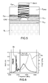
- the final FBAR resonator is produced by depositing an upper metal electrode C M2 at the CAV-formed blister, as illustrated in FIG. figure 5 , furthermore highlighting a zone Z BAW of propagation of acoustic waves of volume.
- the curves of the figure 6 illustrate the electrical response of the suspended membrane obtained according to the method of the invention.
- the curve 6a corresponds to the response of the undissolved piezoelectric layer of the substrate, the curve 6b being relative to said detached diaphragm and thus to the final structure of the FBAR resonator.
- non-bonding initiating zones can be made on the surface of one or both substrates to be assembled to locally prevent the direct bonding of these two substrates and thus to generate at the interface an acoustically decoupling blister. locally these two substrates. It may be in particular hydrocarbon species present on the surface or liquid or solid species. These species can generate gaseous by-products. With a suitable heat treatment, this zone is called to increase in size by the effect of pressure in the unglued zone, so as to generate a suspended membrane zone (side-held). For dimensioning effects we can refer to the articles of Tong and Goesele (book 1999 p.42).
- the bonding energy can be increased during this heat treatment and yet it is not sufficient to prevent the opening of the zone from which the increase of the lateral dimensions r of the unbonded area and its height h.
Abstract
Description
Le domaine de l'invention est celui des filtres à résonateurs à ondes acoustiques. Le développement des télécommunications radiofréquences depuis une dizaine d'années se traduit par un encombrement des bandes de fréquence autorisées. Pour profiter des plages de fréquence disponibles, les systèmes doivent inclure un filtrage de bande, avec une bande de transition étroite. Seuls les filtres à résonateurs en technologie SAW (ondes de surface) ou BAW (ondes de volume), utilisant les propriétés piézoélectriques des matériaux, permettent de tenir ces spécifications avec de faibles pertes et un encombrement réduit. Aujourd'hui, les couches piézoélectriques utilisées pour ces filtres sont réalisées par dépôt (filtres BAW « Bulk Acoustic Wave ») ou à partir de substrats massifs (filtres SAW « Surface Acoustic Wave »).The field of the invention is that of acoustic wave resonator filters. The development of radiofrequency telecommunications over the past decade has resulted in congestion of authorized frequency bands. To take advantage of the available frequency ranges, the systems must include band filtering, with a narrow transition band. Only the resonator filters in SAW (surface wave) or BAW (volume wave) technology, using the piezoelectric properties of the materials, make it possible to meet these specifications with low losses and a small footprint. Today, the piezoelectric layers used for these filters are made by deposition (BAW "Bulk Acoustic Wave" filters) or from massive substrates (SAW "Surface Acoustic Wave" filters).
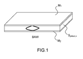
De manière générale, le principe de fonctionnement des composants BAW est illustré en
Les articles suivants retracent une synthèse complète des filtres à base de résonateurs de type BAW et SAW :
Les filtres à ondes de volume existent depuis des dizaines d'années à des fréquences de quelques MHz à quelques dizaines de MHz, utilisant principalement des éléments d'impédance ou des structures à couplage latéral sur quartz pour des applications à bandes étroites, mais leur mise en oeuvre aux radiofréquences ne date que d'une dizaine d'années, suite aux travaux pionniers de Lakin sur l'utilisation de couches piézoélectriques déposées par pulvérisation cathodique à de telles fins. La société Agilent dont la branche « filtre FBAR » (Film Bulk Acoustic Resonator) a donné lieu à la spin-off AVAGO, a été la première à développer un filtre RF à base d'éléments d'impédance tirant parti de films minces de nitrure d'aluminium (AIN), matériau polycristallin déposé. Suite à ces avancées techniques, un grand nombre de chercheurs académiques et industriels se sont lancés sur cette piste, donnant lieu à une activité inventive soutenue durant la présente décennie.Volume-wave filters have existed for tens of years at frequencies from a few MHz to a few tens of MHz, mainly using impedance elements or coupled structures Lateral on quartz for narrow band applications, but their implementation at radio frequencies dates back only ten years, following the pioneering work of Lakin on the use of piezoelectric layers deposited by cathodic sputtering for such purposes. Agilent, whose "Bulk Acoustic Resonator" (FBAR) branch gave rise to the AVAGO spin-off, was the first to develop an RF filter based on impedance elements taking advantage of thin films of nitride of aluminum (AIN), polycrystalline material deposited. Following these technical advances, a large number of academic and industrial researchers have embarked on this track, giving rise to a sustained inventive activity during the present decade.
De manière générale, les résonateurs BAW exploitent la résonance en épaisseur d'une couche piézoélectrique mince qui est isolée acoustiquement du substrat soit par une membrane (technologie FBAR utilisée par AVAGO Technologies), soit par un réseau de Bragg (technologie SMR utilisée par Infineon). Le matériau le plus employé en technologie BAW est à l'heure actuelle le Nitrure d'Aluminium (AIN), qui présente l'avantage d'avoir des coefficients de couplage piézoélectrique de l'ordre de 6.5 %, et également d'avoir de faibles pertes acoustiques et diélectriques, ce qui permet la synthèse de filtres présentant des bandes passantes compatibles avec les spécifications réclamées par la plupart des standards de télécommunication localisés entre 2 et 4 GHz.In general, the BAW resonators exploit the resonance in thickness of a thin piezoelectric layer that is acoustically isolated from the substrate either by a membrane (FBAR technology used by AVAGO Technologies) or by a Bragg grating (SMR technology used by Infineon). . The most used material in BAW technology is currently Aluminum Nitride (AIN), which has the advantage of having piezoelectric coupling coefficients of the order of 6.5%, and also to have low acoustic and dielectric losses, which allows the synthesis of filters with bandwidth compatible with the specifications required by most telecommunications standards located between 2 and 4 GHz.
Néanmoins, plusieurs problèmes continuent à se poser face aux spécifications extrêmement contraignantes présentées par quelques bandes de fréquences, telles que le standard DCS.Nevertheless, several problems continue to arise in the face of the extremely demanding specifications presented by a few frequency bands, such as the DCS standard.
Tout d'abord, les coefficients de couplage piézoélectrique permis par l'AIN n'autorisent pas des bandes passantes relatives supérieures à 6 %. De telles largeurs de bande nécessitent déjà l'utilisation d'électrodes présentant une très forte impédance acoustique (en Molybdène ou en Tungstène), de manière à confiner l'énergie élastique dans la couche piézoélectrique, et des épaisseurs soigneusement déterminées de manière à maximiser leur influence sur le coefficient de couplage piézoélectrique des résonateurs, comme décrits dans les articles suivants :
Des recherches sont menées pour trouver d'autres matériaux présentant des coefficients de couplage piézoélectrique plus élevés, mais force est de constater qu'il n'existe pas d'autre matériau proposant de faibles pertes acoustiques et que l'on sache déposer de manière reproductible et uniforme, comme décrit dans l'article :
A l'inverse, des matériaux monocristallins tels que le Niobate de Lithium ou le Tantalate de Lithium proposent des coefficients de couplages électromécaniques très élevés, permettant la réalisation de filtres présentant des largeurs de bandes relatives de l'ordre de 50 % ;On the other hand, monocrystalline materials such as lithium niobate or lithium tantalate offer very high electromechanical coupling coefficients, making it possible to produce filters having relative bandwidths of the order of 50%;
Ensuite, les standards tels que le DCS nécessitent également à la fois une large bande passante et une forte réjection des standards adjacents. Répondre simultanément à ces deux contraintes nécessite d'utiliser des résonateurs possédant de très forts coefficients de qualité. Bien des travaux ont été menés dans les dix dernières années pour améliorer les propriétés de confinement des ondes acoustiques des résonateurs (
Concernant les résonateurs de type FBAR, Campanella et al. ont réalisé un résonateur FBAR, à partir d'une membrane de nitrure d'Aluminium (AIN) déposée sur une électrode métallique platine/titane. Le substrat utilisé, sur lequel repose ces couches, est du silicium qui a été gravé par plasma réactif (RIE) pour former une cavité. (
Les auteurs Pijolat et al. ont montré la réalisation de tels résonateurs à partir du transfert d'un film mince de LiNbOs sur substrat silicium grâce un procédé basé sur du collage direct et de l'amincissement mécanique (
D'autres auteurs ont proposé de fabriquer une structure FBAR avec une couche de LiNbOs suspendue et dont des caractérisations électriques à 200MHz ont été réalisées :
D'autres types de résonateurs (y compris des résonateurs SAW) sont avantageusement réalisés sur des membranes suspendues.Other types of resonators (including SAW resonators) are advantageously made on suspended membranes.
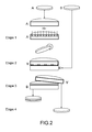
Actuellement, il a déjà été proposé deux principales techniques de report de couches minces : une technique basée sur l'implantation d'ions légers (typiquement hydrogène) et la fracture au niveau de la zone implantée, et la technique précédemment évoquée basée sur un collage et un amincissement mécanique. Ces techniques permettent de reporter une couche monocristalline sur un substrat hôte. Ces techniques sont parfaitement maîtrisées sur silicium permettant entre autres la fabrication industrielle de plaquettes SOI (Silicon On Insulator).Currently, two main thin film transfer techniques have already been proposed: a technique based on the implantation of light ions (typically hydrogen) and the fracture at the level of the implanted zone, and the previously mentioned technique based on a collage and mechanical thinning. These techniques make it possible to postpone a monocrystalline layer on a host substrate. These techniques are perfectly mastered on silicon allowing, among other things, the industrial manufacture of SOI (Silicon On Insulator) wafers.
Le procédé de report par implantation/fracture est notamment décrit dans l'article de
Ce procédé peut être schématiquement résumé par les quatre étapes suivantes illustrées en
- Etape 1 : Un substrat donneur A, par exemple de silicium est implanté par des espèces gazeuses (par exemple de l'hydrogène et/ou des gaz rares) pour former une zone fragile enterrée, délimitant dans ce substrat le film mince à transférer.
- Etape 2 : Le substrat donneur est ensuite assemblé au niveau du film mince précédemment défini, par exemple par collage direct (encore appelé collage moléculaire), avec un substrat de réception B.
- Etape 3 : Une étape de fracture est ensuite obtenue au niveau de la zone fragile enterrée au moyen d'un traitement thermique éventuellement assisté de l'application de contraintes mécaniques. On obtient alors d'une part le film mince solidaire du substrat de réception, et d'autre part le reliquat du substrat donneur correspondant au substrat donneur initial A, pelé du film mince transféré. Ce dernier peut alors être recyclé pour la réalisation d'un autre transfert.
- Etape 4: Eventuellement, des traitements finaux peuvent être réalisés, par exemple un recuit à haute température pour consolider l'interface de collage entre le film mince transféré et le substrat de réception
- Step 1: A donor substrate A, for example silicon, is implanted with gaseous species (for example hydrogen and / or rare gases) to form a buried fragile zone, delimiting in this substrate the thin film to be transferred.
- Step 2: The donor substrate is then assembled at the previously defined thin film, for example by direct bonding (also called molecular bonding), with a receiving substrate B.
- Step 3: A fracture step is then obtained at the level of the buried fragile zone by means of a heat treatment possibly assisted by the application of mechanical stresses. The thin film integral with the receiving substrate is then obtained on the one hand, and the remainder of the donor substrate corresponding to the initial donor substrate A, on the other, peeled off from the transferred thin film. The latter can then be recycled for the realization of another transfer.
- Step 4 : Optionally, final treatments may be performed, for example high temperature annealing to consolidate the bonding interface between the transferred thin film and the receiving substrate
L'épaisseur du film mince transféré est directement reliée à l'énergie d'implantation du faisceau d'ions. A titre d'exemple, l'épaisseur de silicium transférée peut aller de quelques dizaines de nanomètres à quelques micromètres en utilisant un implanteur conventionnel (pour lequel l'énergie d'implantation est typiquement inférieure à 250keV).The thickness of the transferred thin film is directly related to the energy of implantation of the ion beam. For example, the thickness of transferred silicon may range from a few tens of nanometers to a few micrometers using a conventional implanter (for which the implantation energy is typically less than 250 keV).
Les couches transférées sont uniformes et homogènes en épaisseur car définies par une profondeur d'implantation et non par un amincissement mécanique.The transferred layers are uniform and homogeneous in thickness as defined by a depth of implantation and not by mechanical thinning.
Le document
Le document
Alors qu'aujourd'hui dans la majorité des composants pour les MEMS « Micro-Electro-Mechanical Systems », les couches de matériaux piézoélectriques sont réalisées par des techniques de dépôts de type PVD « Plasma Vapor Déposition » et que les couches à élaborer pour ces composants présentent des épaisseurs dans une gamme d'épaisseurs comprises entre quelques centaines de nanomètres et le micromètre, la maîtrise de la fabrication de couches piézoélectriques et électrostrictives monocristallines pour cette gamme d'épaisseurs constitue un verrou technologique important.Whereas today in the majority of components for MEMS "Micro-Electro-Mechanical Systems", the layers of piezoelectric materials are made by PVD-type deposition techniques "Plasma Vapor Deposition" and that the layers to be developed for these components have thicknesses in a range of thicknesses between a few hundred nanometers and the micrometer, mastering the manufacture of single-crystal piezoelectric and electrostrictive layers for this range of thicknesses constitutes an important technological lock.
Dans ce contexte, la présente invention a pour objet un procédé innovant de fabrication d'un résonateur à ondes acoustiques de volume comprenant une membrane comportant une fine couche de matériau piézoélectrique.In this context, the subject of the present invention is an innovative process for manufacturing a volume acoustic wave resonator comprising a membrane comprising a thin layer of piezoelectric material.
Plus précisément l'invention concerne un procédé de fabrication d'un résonateur à ondes acoustiques comprenant une membrane suspendue comportant une couche de matériau piézoélectrique, caractérisé en ce qu'il comprend les étapes suivantes :
- la réalisation d'un premier empilement comportant au moins une couche de premier matériau piézoélectrique à la surface d'un premier substrat ;
- la réalisation d'un second empilement comprenant au moins un second substrat ;
- la réalisation d'au moins une zone initiatrice de non collage par dépôt ou création de particules de tailles maîtrisées laissant la surface d'un desdits empilements dotée localement de nanostructures en saillie avant une étape subséquente de collage ;
- le collage direct desdits deux empilements créant une cloque entre les empilements, due à la présence de la zone initiatrice de non collage ;
- l'amincissement du premier empilement pour éliminer au moins le premier substrat.
- performing a first stack comprising at least one layer of first piezoelectric material on the surface of a first substrate;
- performing a second stack comprising at least a second substrate;
- providing at least one non-sticking initiation zone by deposition or creation of controlled size particles leaving the surface of one of said stacks locally provided with protruding nanostructures before a subsequent bonding step;
- direct bonding of said two stacks creating a blister between the stacks, due to the presence of the non-bonding initiator zone;
- thinning the first stack to remove at least the first substrate.
Par collage direct, on entend tout type de collage ne nécessitant pas la présence d'une substance adhésive. Il peut s'agir avantageusement d'un collage par contact direct mais il peut s'agir également d'un collage par thermocompression ou d'un collage anodique ou encore d'un collage par fusion (« fusion bonding » en anglais).By direct bonding is meant any type of bonding that does not require the presence of an adhesive substance. It can be advantageously a direct contact bonding but it can also be a bonding by thermocompression or anodic bonding or fusion bonding.
La zone initiatrice de non collage a ainsi pour but d'empêcher localement le collage entre les deux empilements à son endroit ou son voisinage, générant ainsi une cloque entre la couche de premier matériau piézoélectrique et le second empilement, permettant le découplage acoustique local de ces deux éléments.The non-bonding initiator zone thus aims to locally prevent bonding between the two stacks at its place or neighborhood, thus generating a blister between the layer of first piezoelectric material and the second stack, allowing local acoustic decoupling of these layers. two elements.
Les nanostructures ont des dimensions latérales (dans le plan du substrat) inférieures à 1 micron et avantageusement comprise entre 10 et 100 nm.The nanostructures have lateral dimensions (in the plane of the substrate) of less than 1 micron and advantageously of between 10 and 100 nm.
L'invention permet ainsi de réaliser des membranes suspendues collectivement sur une plaque (wafer en anglais) avec des dimensions latérales allant de 100 microns au millimètre.The invention thus makes it possible to produce membranes hung collectively on a wafer plate with lateral dimensions ranging from 100 microns to millimeters.
Avantageusement, une étape de traitement thermique peut être réalisée pendant ou après l'étape de collage direct afin de favoriser la création et/ou la croissance de la cloque. Typiquement, ce traitement thermique peut avoir lieu à une température comprise entre 100°C et 500°C. Cette étape peut également permettre à deux ou plusieurs cloques contigües de se rejoindre pour former une cloque de dimension supérieure.Advantageously, a heat treatment step can be performed during or after the direct bonding step to promote the creation and / or growth of the blister. Typically, this heat treatment can take place at a temperature between 100 ° C and 500 ° C. This step may also allow two or more contiguous blisters to join together to form a larger size blister.
La zone initiatrice de non collage peut être une nanostructure en saillie c'est-à-dire une excroissance locale par rapport à la surface de dimensions submicroniques. La cloque générée s'étend alors de part et d'autres de cette nanostructure.The non-bonding initiator zone may be a protruding nanostructure, that is to say a local protrusion with respect to the surface of submicron dimensions. The generated blister then extends on both sides of this nanostructure.
Selon une variante de l'invention, l'étape de réalisation de cette nanostructure en saillie est effectuée par lithographie et gravure.According to a variant of the invention, the step of producing this protruding nanostructure is carried out by lithography and etching.
Selon une variante de l'invention, l'étape de réalisation de cette nanostructure en saillie est effectuée par le dépôt de particules de taille contrôlée et de manière localisée.According to a variant of the invention, the step of producing this protruding nanostructure is carried out by depositing particles of controlled size and in a localized manner.
Selon une variante de l'invention, la nanostructure en saillie présentant une hauteur de l'ordre de quelques dizaines à quelques centaines de nanomètres, la cloque présente une étendue de diamètre de l'ordre d'un millier de micromètres.According to a variant of the invention, the protruding nanostructure having a height of the order of a few tens to a few hundred nanometers, the blister has a diameter range of the order of a thousand micrometers.
Il est à noter que le traitement thermique réalisé pendant ou après l'étape de collage, peut permettre également de décoller localement la surface de la nanostructure en saillie de la surface de l'empilement en regard.It should be noted that the heat treatment carried out during or after the gluing step, may also allow local takeoff surface of the nanostructure projecting from the surface of the stack opposite.
De même, la surface entourant la nanostructure en saillie ou celle en regard de celle-ci peut avoir été préparée préalablement au collage pour faciliter ou pour adapter l'extension de la cloque lors du traitement thermique par exemple.Similarly, the surface surrounding the projecting nanostructure or that facing it may have been prepared prior to bonding to facilitate or to adapt the extension of the blister during heat treatment for example.
Cette préparation peut notamment consister à diminuer l'hydrophilie et/ou à augmenter la rugosité de la surface si l'on souhaite favoriser l'extension latérale de la cloque et réciproquement.This preparation may in particular consist of reducing the hydrophilicity and / or increasing the roughness of the surface if it is desired to promote the lateral extension of the blister and vice versa.
Pour modifier l'hydrophilie, on peut avoir recours par exemple à un traitement plasma ou UV/ozone. Pour modifier la rugosité, on peut avoir recours par exemple à une gravure chimique, humide ou sèche.To modify the hydrophilicity, it is possible to use, for example, a plasma or UV / ozone treatment. To modify the roughness, it is possible to use for example a chemical etching, wet or dry.
Selon une variante de l'invention, la zone initiatrice de non collage est obtenue par le dépôt localisé d'hydrocarbures ou de produits liquides ou solides pouvant générer des sous-produits gazeux, par exemple à l'aide d'une pointe de microscope à force atomique (AFM). Cette zone crée une zone de non collage ou cloque qui peut être appelée à croitre en dimension par effet de pression dans la zone non collée suite à un traitement thermique.According to a variant of the invention, the non-sticking initiator zone is obtained by the localized deposition of hydrocarbons or liquid or solid products that can generate gaseous by-products, for example with the aid of a microscope tip. Atomic Force (AFM). This zone creates a zone of non-sticking or blistering which may be called to increase in size by the effect of pressure in the unglued zone following a heat treatment.
Avantageusement, le premier empilement et/ou le second empilement peuvent comporter en surface une couche de collage, au niveau de laquelle le collage direct est effectué.Advantageously, the first stack and / or the second stack may comprise on the surface a bonding layer, at which direct bonding is performed.
Avantageusement, le premier empilement peut comporter entre la couche de premier matériau piézoélectrique et l'éventuelle couche de collage (ou la surface) une couche métallique destinée à servir d'électrode.Advantageously, the first stack may comprise between the layer of first piezoelectric material and the optional bonding layer (or the surface) a metal layer intended to serve as an electrode.
Avantageusement, le premier matériau piézoélectrique est monocristallin. Une telle couche peut être obtenue par épitaxie sur un substrat adapté ou constituée la partie superficielle du premier substrat. Dans ce cas, le premier substrat peut être un substrat massif du premier matériau piézoélectrique. La couche peut également être déposée sur le premier substrat.Advantageously, the first piezoelectric material is monocrystalline. Such a layer can be obtained by epitaxy on a suitable substrate or constituted by the superficial portion of the first substrate. In this case, the first substrate may be a solid substrate of the first piezoelectric material. The layer may also be deposited on the first substrate.
Selon une variante de l'invention, le procédé comporte en outre une étape d'implantation ionique de manière à créer dans le premier empilement une zone fragile enterrée délimitant avec la surface dudit empilement une zone comportant au moins en partie la couche de premier matériau piézoélectrique.According to a variant of the invention, the method further comprises an ion implantation step so as to create in the first stack a buried fragile zone delimiting with the surface of said stack an area comprising at least partly the layer of first piezoelectric material .
Selon cette variante de l'invention, l'amincissement est alors obtenu par fracture au niveau de la zone fragile enterrée.According to this variant of the invention, the thinning is then obtained by fracture at the buried fragile zone.
Selon une autre variante de l'invention, l'amincissement est obtenu par meulage (« grinding » en anglais) et polissage.According to another variant of the invention, the thinning is obtained by grinding ("grinding" in English) and polishing.
Avantageusement, l'étape de polissage est une étape de polissage mécano-chimique (plus connu sous l'acronyme CMP (chemical and mechanical polishing)). Ce polissage est réalisé par exemple à l'aide d'une solution contenant un abrasif (« slurry » en anglais), par exemple à base de silice colloïdale.Advantageously, the polishing step is a chemical mechanical polishing step (better known by the acronym CMP (chemical and mechanical polishing)). This polishing is carried out for example using a solution containing an abrasive ("slurry" in English), for example based on colloidal silica.
Selon une variante de l'invention, le matériau piézoélectrique est en LiNbOs ou en LiTaO3 ou plus généralement en Li(TaxNb1-x)O3. Si la couche est déposée, le matériau piézoélectrique peut être en AIN ou PZT notamment.According to a variant of the invention, the piezoelectric material is LiNbO s or LiTaO 3 or more generally Li (TaxNb1-x) O3. If the layer is deposited, the piezoelectric material may be AlN or PZT in particular.
Selon une variante de l'invention, le second substrat est en silicium ou en quartz ou en diamant ou encore en saphir. Il peut être simple ou composite.According to a variant of the invention, the second substrate is silicon or quartz or diamond or sapphire. It can be simple or composite.
Selon une variante de l'invention, au moins une couche de collage est en matériau diélectrique pouvant être en SiO2.According to a variant of the invention, at least one bonding layer is made of dielectric material that can be SiO 2 .
Selon une variante de l'invention, le procédé comprend en outre une étape de définition d'électrode dans ladite couche métallique.According to a variant of the invention, the method further comprises an electrode definition step in said metal layer.
Selon une variante de l'invention, le procédé comprend en outre une étape de réalisation d'une électrode supérieure à la surface de l'empilement final des premier et second empilements après l'étape d'amincissement.According to a variant of the invention, the method further comprises a step of producing an upper electrode on the surface of the final stack of the first and second stacks after the thinning step.
L'invention sera mieux comprise et d'autres avantages apparaîtront à la lecture de la description qui va suivre et grâce aux figures annexées parmi lesquelles :
- la
figure 1 illustre le principe de fonctionnement des composants BAW mettant en évidence la propagation des ondes acoustiques de volume ; - la
figure 2 illustre les différentes étapes d'un procédé de report de substrats par implantation/fracture selon l'art connu ; - les
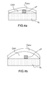
figures 3a à 3e illustrent les différentes étapes d'un exemple de procédé de fabrication d'un résonateur de type FBAR selon l'invention ; - les
figures 4a et 4b schématisent la cloque créée lors d'une étape du procédé de fabrication selon l'invention, avant et après, une opération de traitement thermique ; - la
figure 5 illustre un résonateur de type FBAR réalisé selon le procédé de l'invention ; - la
figure 6 illustre la réponse électrique de la membrane non décollée du substrat (courbe 6a) et la réponse de la membrane suspendue (courbe 6b) ;
- the
figure 1 illustrates the principle of operation of BAW components highlighting the propagation of acoustic waves volume; - the
figure 2 illustrates the different steps of a substrate transfer method by implantation / fracture according to the prior art; - the
Figures 3a to 3e illustrate the different steps of an exemplary method of manufacturing a FBAR resonator according to the invention; - the
Figures 4a and 4b schematize the blister created during a step of the manufacturing process according to the invention, before and after, a heat treatment operation; - the
figure 5 illustrates a FBAR resonator made according to the method of the invention; - the
figure 6 illustrates the electrical response of the undissolved membrane of the substrate (curve 6a) and the response of the suspended membrane (curve 6b);
De manière générale le procédé de la présente invention permet de réaliser des composants à ondes acoustiques, par exemple des composants à ondes acoustiques de volume et notamment des composants de type résonateur FBAR comportant une membrane suspendue de matériau piézoélectrique avec une électrode inférieure et une électrode supérieure de manière à générer la propagation d'ondes acoustiques de volume, ladite membrane étant réalisée à la surface d'une cloque créée à partir de l'assemblage par collage de deux supports, l'un comportant à sa surface au moins une zone initiatrice de non collage, par exemple une nanostructure en saillie.In general, the method of the present invention makes it possible to produce acoustic wave components, for example volume acoustic wave components and in particular FBAR resonator type components comprising a suspended membrane of piezoelectric material with a lower electrode and an upper electrode. in order to generate the propagation of acoustic waves of volume, said membrane being made on the surface of a blister created from the assembly by gluing of two supports, one having on its surface at least one initiating zone of non-bonding, for example a protruding nanostructure.
La membrane de matériau suspendue comprend une fine couche de matériau piézoélectrique. Le procédé pour réaliser une telle membrane peut se baser sur un procédé connu et maîtrisé comportant l'implantation d'un substrat massif de matériau piézoélectrique pour créer dans ce substrat une zone fragile enterrée délimitant dans ce substrat ladite fine couche puis la séparation de ladite fine couche de matériau piézoélectrique de l'ensemble du substrat piézoélectrique par fracture au niveau de cette zone fragile par exemple par traitement thermique éventuellement assisté de forces mécaniques.The suspended material membrane comprises a thin layer of piezoelectric material. The method for producing such a membrane can be based on a known and controlled method comprising the implantation of a solid substrate of piezoelectric material to create in this substrate a buried fragile zone delimiting in said substrate said thin layer and then the separation of said thin layer of piezoelectric material of the entire piezoelectric substrate by fracture at this fragile zone for example by heat treatment possibly assisted by mechanical forces.
Un substrat piézoélectrique SPiezo (par exemple de type LiNbO3, LiTaO3 ...) massif, est choisi pour l'application BAW (en terme d'orientation, de nature de matériau ...). Il pourrait s'agir en variante d'un substrat support (de silicium par exemple) présentant uniquement une couche superficielle de matériau piézoélectrique. Il comprend avantageusement un empilement d'au moins une couche métallique CM1 destinée à être une électrode enterrée pour le résonateur final. Cette couche métallique peut être à base de Cu, AlCu, AlSi, W, Mo, Pt, Cr ....A Piezo S piezoelectric substrate (for example of the LiNbO 3 , LiTaO 3, etc.) type is chosen for the BAW application (in terms of orientation, nature of material, etc.). It could alternatively be a support substrate (of silicon, for example) having only a surface layer of piezoelectric material. It advantageously comprises a stack of at least one metal layer C M1 intended to be a buried electrode for the final resonator. This metal layer may be based on Cu, AlCu, AlSi, W, Mo, Pt, Cr ....
L'ensemble de l'empilement est ensuite éventuellement recouvert avec une couche de collage CC1, il peut s'agir par exemple d'une couche diélectrique, par exemple de SiO2 de quelques centaines de nm (par exemple 200 nm) en surface destinée à faciliter l'opération ultérieure de collage direct, comme illustré en
Une opération d'implantation ionique est réalisée (avant ou après le dépôt des couches métallique et de collage) dans le substrat massif piézoélectrique afin de créer une zone fragile enterrée Zfr délimitant dans ce substrat la couche mince de matériau piézoélectrique à transférer. Cette implantation peut être effectuée par exemple à base d'hydrogène ou d'hélium ou un mélange de ces deux espèces avec des doses entre 1016 et 1017 at/cm2 et ce avec une énergie comprise entre 50 keV et 250 keV selon l'épaisseur de la couche piézoélectrique choisie, comme illustré en
En parallèle on réalise sur un second substrat S2 qui peut être en matériau piézoélectrique ou non, par exemple Si, Saphir, Quartz ..., le dépôt d'une couche de collage, par exemple diélectrique par exemple de SiO2 en surface destinée à l'opération de collage, comme illustré en
Les substrats sont ensuite préparés, par exemple par polissage mécano-chimique, pour être compatible avec l'étape ultérieure de collage directe. Cette préparation peut permettre d'obtenir la planéité et la rugosité souhaitée pour le collage direct ultérieur.The substrates are then prepared, for example by chemical mechanical polishing, to be compatible with the subsequent step of direct bonding. This preparation can make it possible to obtain the flatness and the desired roughness for the subsequent direct bonding.
Durant/après cette étape, des particules de tailles maitrisées sont déposées/créées sur l'une des deux interfaces de collage. Ces particules ou µ-plots peuvent, par exemple, être créées par lithographie suivie d'une gravure ou encore par le dépôt de particules de taille contrôlée et de manière localisée. La
La
Les deux substrats sont ensuite collés par collage direct comme illustré dans l'article: Tong & Gösele 1999,
Appliqué au cas du niobate de lithium (en termes de coefficient de déformation et énergie de surface correspondante au matériau), les ordres de grandeurs des rayons des cloques trouvés par calcul théorique et ceux trouvés expérimentalement sont en adéquation.Applied to the case of lithium niobate (in terms of the deformation coefficient and surface energy corresponding to the material), the orders of magnitude of the radii of the blisters found by theoretical calculation and those found experimentally are in adequacy.
Dans le cas de la présente invention, la demanderesse a observé que la hauteur des bulles de gaz est nettement supérieure à la hauteur des particules : le diamètre et la hauteur des cloques sont contrôlés par le budget thermique appliqué.In the case of the present invention, the Applicant has observed that the height of the gas bubbles is significantly greater than the height of the particles: the diameter and height of the blisters are controlled by the thermal budget applied.
Selon le procédé de la présente invention, un traitement thermique est appliqué (entre 100°C et 500°C, préférentiellement 250°C) afin d'initier le transfert du film mince de matériau piézoélectrique par fracture au niveau de la zone fragile enterré. Ce traitement thermique permet également de faire croitre la cloque initialement formée autour de la nanostructure en saillie. Sur les zones sans particules et hors des zones de cloques induites, le collage direct des faces est réalisé.According to the method of the present invention, a heat treatment is applied (between 100 ° C. and 500 ° C., preferably 250 ° C.) in order to initiate the transfer of the thin film of piezoelectric material by fracture to the buried fragile zone. This heat treatment also makes it possible to grow the initially formed blister around the protruding nanostructure. On areas without particles and out of induced blistering areas, direct bonding of the faces is achieved.
L'application d'un budget thermique supplémentaire (une fois la fracture obtenue) par exemple entre 100 et 500°C (préférentiellement autour de 250 °C) permet de contrôler les dimensions latérales de cloques souhaitées. Il peut permettre également de décoller la membrane de la nanostructure en saillie (comme illustré
Ce budget thermique peut également permettre à deux ou plusieurs cloques contigües de se rejoindre pour former une cloque de grande dimension.This thermal budget can also allow two or more contiguous blisters to join together to form a large blister.
Une couche additionnelle d'encapsulation peut être déposée pour figer la structure. Les
Typiquement, pour des particules de l'ordre de 100 nm de hauteur, la cloque maximale atteinte est de l'ordre de 1000 µm de diamètre.Typically, for particles of the order of 100 nm in height, the maximum blister attained is of the order of 1000 μm in diameter.
Des procédés de finition (tel que traitement thermique et/ou polissage pour obtenir une rugosité compatible avec la réalisation de composants a posteriori) peuvent être effectués.Finishing processes (such as heat treatment and / or polishing to obtain a roughness compatible with the production of components a posteriori) can be performed.
On obtient ainsi une couche fine de matériau piézoélectrique CPiézo avec couches additionnelles sur un substrat hôte. Le résonateur FBAR final est réalisé par dépôt d'une électrode métallique supérieure CM2 au niveau de la cloque formée CAV, comme illustré en
Des tests électriques ont été réalisés sur une telle structure montrant le caractère piézoélectrique résonant de la membrane suspendue. Les courbes de la
Comme évoqué précédemment, d'autres type de zones initiatrices de non collage peuvent être réalisées à la surface d'un ou des deux substrats à assembler pour prévenir localement le collage direct de ces deux substrats et générer ainsi à l'interface une cloque découplant acoustiquement localement ces deux substrats. Il peut s'agir notamment d'espèces hydrocarbures présentes en surface ou d'espèces liquides ou solides. Ces espèces peuvent générer des sous produits gazeux. Avec un traitement thermique adapté, cette zone est appelée à croitre en dimension par effet de pression dans la zone non collée, de façon à générer une zone de membrane suspendue (à tenue latérale). Pour les effets de dimensionnement on peut se rapporter aux articles de Tong et Goesele (book 1999 p.42).As mentioned above, other types of non-bonding initiating zones can be made on the surface of one or both substrates to be assembled to locally prevent the direct bonding of these two substrates and thus to generate at the interface an acoustically decoupling blister. locally these two substrates. It may be in particular hydrocarbon species present on the surface or liquid or solid species. These species can generate gaseous by-products. With a suitable heat treatment, this zone is called to increase in size by the effect of pressure in the unglued zone, so as to generate a suspended membrane zone (side-held). For dimensioning effects we can refer to the articles of Tong and Goesele (book 1999 p.42).
Dans le cas d'un dégazage, l'article de F. Rieutord (ECS201 0) donne par exemple la dimension rayon critique Rc de bulles (zones non collées) en fonction de la pression (traduire le nombre N de molécules ou d'atomes disponible) à une température donnée. Rc est une valeur où la bulle est stable à une température T donnée.In the case of degassing, the article by F. Rieutord (ECS201 0) gives, for example, the critical radius dimension Rc of bubbles (unglued zones) as a function of the pressure (translate the number N of molecules or atoms available) at a given temperature. Rc is a value where the bubble is stable at a given temperature T.
Lors du traitement thermique, la pression augmente comme PV= NRT. L'énergie de collage peut être augmentée lors de ce traitement thermique et pourtant elle n'est pas suffisante pour empêcher l'ouverture de la zone d'où l'augmentation des dimensions latérales r de la zone non collée et de sa hauteur h.During the heat treatment, the pressure increases as PV = NRT. The bonding energy can be increased during this heat treatment and yet it is not sufficient to prevent the opening of the zone from which the increase of the lateral dimensions r of the unbonded area and its height h.
De plus si r est supérieur à un rayon critique tel que défini dans l'article de F. Rieutord (ECS 2010) ou Tong et Goesele (book 1999 p.42), la zone non collée ne se résorbe pas.Moreover, if r is greater than a critical radius as defined in the article by F. Rieutord (ECS 2010) or Tong and Goesele (book 1999 p.42), the unbound area is not absorbed.
Ces contaminations contrôlées permettent d'induire des zones non collées supérieures à une taille critique.These controlled contaminations allow inducing unbound areas greater than a critical size.
Dans la réalisation, on peut déposer un contaminant pouvant dégazer sur la surface de la zone de collage par pointe AFM par exemple.In the embodiment, it is possible to deposit a contaminant capable of degassing on the surface of the AFM tip bonding zone, for example.
Claims (24)
Applications Claiming Priority (1)
| Application Number | Priority Date | Filing Date | Title |
|---|---|---|---|
| FR1060358A FR2968861B1 (en) | 2010-12-10 | 2010-12-10 | METHOD FOR MANUFACTURING ACOUSTIC WAVE RESONATOR COMPRISING A SUSPENDED MEMBRANE |
Publications (2)
| Publication Number | Publication Date |
|---|---|
| EP2464006A1 true EP2464006A1 (en) | 2012-06-13 |
| EP2464006B1 EP2464006B1 (en) | 2018-05-30 |
Family
ID=45044460
Family Applications (1)
| Application Number | Title | Priority Date | Filing Date |
|---|---|---|---|
| EP11191911.4A Active EP2464006B1 (en) | 2010-12-10 | 2011-12-05 | Method for manufacturing an acoustic-wave resonator including a suspended membrane |
Country Status (8)
| Country | Link |
|---|---|
| US (1) | US8715517B2 (en) |
| EP (1) | EP2464006B1 (en) |
| JP (1) | JP6047789B2 (en) |
| KR (1) | KR101910195B1 (en) |
| CN (1) | CN102545814B (en) |
| FR (1) | FR2968861B1 (en) |
| SG (1) | SG184621A1 (en) |
| TW (1) | TWI562412B (en) |
Cited By (1)
| Publication number | Priority date | Publication date | Assignee | Title |
|---|---|---|---|---|
| EP3706180A1 (en) * | 2019-03-05 | 2020-09-09 | Commissariat à l'Energie Atomique et aux Energies Alternatives | Method for manufacturing a micro-electro-mechanical system produced from a deposited piezoelectric or ferroelectric layer |
Families Citing this family (12)
| Publication number | Priority date | Publication date | Assignee | Title |
|---|---|---|---|---|
| FR2951336B1 (en) | 2009-10-09 | 2017-02-10 | Commissariat A L'energie Atomique | ACOUSTIC WAVE DEVICE COMPRISING A SURFACE WAVE FILTER AND A VOLUME WAVE FILTER AND METHOD OF MANUFACTURE |
| FR2974691B1 (en) | 2011-04-28 | 2019-08-30 | Commissariat A L'energie Atomique Et Aux Energies Alternatives | ELECTRO-MECHANICAL DEVICE WITH ACOUSTIC WAVES COMPRISING A TRANSDUCTION ZONE AND AN EXTENDED CAVITY |
| FR2976126B1 (en) | 2011-06-01 | 2014-05-09 | Commissariat Energie Atomique | ELECTRICAL COMPONENT COMPRISING PEROVSKITE STRUCTURAL MATERIAL AND OPTIMIZED ELECTRODES AND METHOD OF MANUFACTURE |
| DE102013019434A1 (en) * | 2013-11-20 | 2015-05-21 | Berliner Glas Kgaa Herbert Kubatz Gmbh & Co. | Solid body joining of a carrier body and a cover layer, in particular by anodic bonding |
| KR102207928B1 (en) | 2014-08-13 | 2021-01-26 | 삼성전자주식회사 | Audio sensing device and method of acquiring frequency information |
| JP6396854B2 (en) * | 2015-06-02 | 2018-09-26 | 信越化学工業株式会社 | Method for manufacturing composite wafer having oxide single crystal thin film |
| TWI625446B (en) * | 2015-06-18 | 2018-06-01 | 德克薩斯大學體系董事會 | Resonator, resonator array for damping acoustic energy from source in liquid and noise abatement system |
| WO2018182657A1 (en) * | 2017-03-30 | 2018-10-04 | Intel Corporation | Compensation for temperature coefficient of resonant frequency using atomic layer deposition materials |
| CN108365083B (en) * | 2018-02-07 | 2022-03-08 | 济南晶正电子科技有限公司 | Method for manufacturing composite piezoelectric substrate for surface acoustic wave device |
| CN109981069B (en) * | 2019-03-13 | 2022-03-15 | 电子科技大学 | Method for preparing film bulk acoustic wave resonator with isolation layer and bulk acoustic wave resonator |
| CN111884616B (en) * | 2020-07-23 | 2021-04-13 | 中国科学院上海微系统与信息技术研究所 | Substrate/piezoelectric material thin film structure and preparation method and application thereof |
| FR3132788B1 (en) * | 2022-02-14 | 2024-01-05 | Soitec Silicon On Insulator | METHOD FOR TRANSFERRING A THIN LAYER TO A SUPPORT SUBSTRATE |
Citations (4)
| Publication number | Priority date | Publication date | Assignee | Title |
|---|---|---|---|---|
| EP0741910A1 (en) | 1994-01-26 | 1996-11-13 | Commissariat A L'energie Atomique | Cavity-containing structure and method for making same |
| EP0851465A1 (en) | 1996-12-09 | 1998-07-01 | Commissariat A L'energie Atomique | Method of separation of at least two elements joined by ion implantation |
| US20030199105A1 (en) * | 2002-04-22 | 2003-10-23 | Kub Francis J. | Method for making piezoelectric resonator and surface acoustic wave device using hydrogen implant layer splitting |
| US20050255234A1 (en) * | 2004-04-23 | 2005-11-17 | Atsuhiko Kanda | Method for manufacturing resonator |
Family Cites Families (23)
| Publication number | Priority date | Publication date | Assignee | Title |
|---|---|---|---|---|
| JPS506158B1 (en) * | 1970-07-08 | 1975-03-11 | ||
| JPS5226664B2 (en) * | 1972-02-10 | 1977-07-15 | ||
| KR930011385B1 (en) * | 1988-11-07 | 1993-12-04 | 마쯔시다덴기산교 가부시기가이샤 | Dielectric resonator, method of producing the same and plating device therefor |
| KR20030039446A (en) * | 2001-11-13 | 2003-05-22 | 삼성전자주식회사 | Fabrication of Film Bulk Acoustic Resonator |
| US7830074B2 (en) * | 2006-08-08 | 2010-11-09 | Hrl Laboratories, Llc | Integrated quartz oscillator on an active electronic substrate |
| JP4149416B2 (en) * | 2004-05-31 | 2008-09-10 | 富士通メディアデバイス株式会社 | Piezoelectric thin film resonator, filter, and manufacturing method thereof |
| JP4820609B2 (en) * | 2004-09-10 | 2011-11-24 | パナソニック株式会社 | Filter module, duplexer, communication device using piezoelectric resonator, and manufacturing method thereof |
| JP2006101005A (en) * | 2004-09-28 | 2006-04-13 | Toshiba Corp | Thin-film piezoelectric resonator and manufacturing method thereof, and method for manufacturing high-frequency circuit package body |
| JP4707503B2 (en) * | 2005-08-25 | 2011-06-22 | パナソニック株式会社 | Thin film bulk acoustic resonator |
| JP2007213825A (en) * | 2006-02-07 | 2007-08-23 | Matsushita Electric Ind Co Ltd | Nonaqueous electrolyte secondary battery, anode activator and anode of the same, as well as manufacturing method of nonaqueous electrolyte secondary battery, anode activator, and anode of the same |
| JP2007221588A (en) * | 2006-02-17 | 2007-08-30 | Toshiba Corp | Thin film piezoelectric resonator, and method of manufacturing same |
| TW200818691A (en) * | 2006-08-08 | 2008-04-16 | Hrl Lab Llc | An integrated quartz oscillator on an active electronic substrate |
| JP2008252159A (en) * | 2007-03-29 | 2008-10-16 | Ngk Insulators Ltd | Ladder type piezoelectric filter |
| FR2921192B1 (en) | 2007-09-17 | 2010-08-20 | Commissariat Energie Atomique | SOLID IMMERSION LENS AND METHOD OF MAKING THE SAME |
| JP2009124640A (en) * | 2007-11-19 | 2009-06-04 | Hitachi Media Electoronics Co Ltd | Thin-film piezoelectric bulk wave resonator and its manufacturing method, and thin-film piezoelectric bulk wave resonator filter using thin-film piezoelectric bulk wave resonator |
| JP5168568B2 (en) * | 2008-09-01 | 2013-03-21 | Tdk株式会社 | Thin film bulk wave resonator |
| JP4743258B2 (en) * | 2008-10-31 | 2011-08-10 | 株式会社村田製作所 | Method for manufacturing piezoelectric device |
| US8507860B2 (en) * | 2009-05-20 | 2013-08-13 | Nutech Ventures | Terahertz resonator |
| FR2950197A1 (en) | 2009-09-15 | 2011-03-18 | Commissariat Energie Atomique | OPTIMIZED OPTIONAL PIEZOELECTRIC MEMBRANE AND PROCESS FOR MANUFACTURING THE MEMBRANE |
| FR2951014B1 (en) | 2009-10-06 | 2011-11-25 | Commissariat Energie Atomique | PIEZOELECTRIC ACTUATION STRUCTURE COMPRISING AN INTEGRATED PIEZORESISTIVE STRAIN GAUGE AND METHOD FOR PRODUCING THE SAME |
| FR2953647B1 (en) | 2009-12-04 | 2011-11-25 | Commissariat Energie Atomique | METHOD FOR PRODUCING AN ACOUSTIC VOLTAGE RESONATOR OF FBAR TYPE VOLUMES |
| FR2962613B1 (en) | 2010-07-06 | 2013-08-16 | Commissariat Energie Atomique | DEVICE FOR IMPEDANCE ADAPTATION OF A COMPONENT COMPRISING AN ADAPTABLE IMPEDANCE FILTER BASED ON PEROVSKITE MATERIAL |
| FR2964497B1 (en) | 2010-09-03 | 2013-04-19 | Commissariat Energie Atomique | INTEGRATED CAPACITY COMPRISING AN ELECTRIC INSULATION LAYER OF AMORPHOUS PEROVSKITE MATERIAL AND METHOD OF MANUFACTURE |
-
2010
- 2010-12-10 FR FR1060358A patent/FR2968861B1/en not_active Expired - Fee Related
-
2011
- 2011-12-05 EP EP11191911.4A patent/EP2464006B1/en active Active
- 2011-12-06 SG SG2011090834A patent/SG184621A1/en unknown
- 2011-12-08 US US13/314,844 patent/US8715517B2/en active Active
- 2011-12-09 TW TW100145537A patent/TWI562412B/en active
- 2011-12-09 JP JP2011270459A patent/JP6047789B2/en active Active
- 2011-12-09 CN CN201110462242.9A patent/CN102545814B/en active Active
- 2011-12-09 KR KR1020110132303A patent/KR101910195B1/en active IP Right Grant
Patent Citations (4)
| Publication number | Priority date | Publication date | Assignee | Title |
|---|---|---|---|---|
| EP0741910A1 (en) | 1994-01-26 | 1996-11-13 | Commissariat A L'energie Atomique | Cavity-containing structure and method for making same |
| EP0851465A1 (en) | 1996-12-09 | 1998-07-01 | Commissariat A L'energie Atomique | Method of separation of at least two elements joined by ion implantation |
| US20030199105A1 (en) * | 2002-04-22 | 2003-10-23 | Kub Francis J. | Method for making piezoelectric resonator and surface acoustic wave device using hydrogen implant layer splitting |
| US20050255234A1 (en) * | 2004-04-23 | 2005-11-17 | Atsuhiko Kanda | Method for manufacturing resonator |
Non-Patent Citations (13)
| Title |
|---|
| F. RIEUTORD, ECS, 2010 |
| H. CAMPANELLA; J. ESTEVE; E. MARTINCIC; P. NOUET; A. URANGA; N. BARNIOL, IEEE SENSORS, 2008 |
| J. KAITILA: "Review of wave propagation in BAW thin film devices: progress and prospects", PROCEEDINGS OF THE 2007 IEEE ULTRASONICS SYMPOSIUM, 2007 |
| M. BRUEL: "Silicon on insulator material technology", ELECTRONIC LETTERS, vol. 31, no. 14, 1995, pages 1201 - 1202, XP006003062, DOI: doi:10.1049/el:19950805 |
| M. PIJOLAT; S. LOUBRIAT; S. QUESTE; D. MERCIER; A. REINHARDT; E. DEFAŸ; C. DEGUET; L. CLAVELIER; H. MORICEAU; M. AÏD, APPL. PHYS. LETT, vol. 95, 2009, pages 182106 |
| P. MURALT ET AL.: "Ils there a better material for thin film BAW applications than AIN", PROCEEDINGS OF THE 2005 IEEE ULTRASONICS SYMPOSIUM |
| P. MURALT ET AL.: "Is there a better material for thin film BAW applications than AIN", PROCEEDINGS OF THE 2005 IEEE ULTRASONICS SYMPOSIUM., 2005 |
| PIJOLAT M ET AL: "Large electromechanical coupling factor film bulk acoustic resonator with X-cut LiNbO3 layer transfer", APPLIED PHYSICS LETTERS, AIP, vol. 95, no. 18, 5 November 2009 (2009-11-05), pages 182106 - 182106, XP012126324 * |
| R. AIGNER: "Bringing BAW technology into volume production : the Ten Commandments and the seven deadly sins", PROCEEDINGS OF THE THIRD INTERNATIONAL SYMPOSIUM ON ACOUSTIC WAVE DEVICES FOR FUTURE MOBILE COMMUNICATION SYSTEMS, 2007 |
| R. AIGNER: "Bringing BAW technology into volume production: the Ten Commandments and the seven deadly sins", PROCEEDINGS OF THE THIRD INTERNATIONAL SYMPOSIUM ON ACOUSTIC WAVE DEVICES FOR FUTURE MOBILE COMMUNICATION SYSTEMS, 2007 |
| TONG Q-Y ET AL: "Semiconductor wafer bonding: recent developments", MATERIALS CHEMISTRY AND PHYSICS, ELSEVIER, vol. 37, no. 2, 1 March 1994 (1994-03-01), pages 101 - 127, XP024148341 * |
| TONG; GÔSELE; Q.-Y. TONG; U. GÔSELE: "Semiconductor Wafer Bonding: Science and Technology", 1999, WILEY, pages: 297 |
| W. STEICHEN; S. BALLANDRAS: "Composants acoustiques utilisés pour le filtrage : revues de différentes technologies", EDITIONS DE TECHNIQUES DE L'INGÉNIEUR, 2008, pages E-2000,31 |
Cited By (4)
| Publication number | Priority date | Publication date | Assignee | Title |
|---|---|---|---|---|
| EP3706180A1 (en) * | 2019-03-05 | 2020-09-09 | Commissariat à l'Energie Atomique et aux Energies Alternatives | Method for manufacturing a micro-electro-mechanical system produced from a deposited piezoelectric or ferroelectric layer |
| FR3093511A1 (en) * | 2019-03-05 | 2020-09-11 | Commissariat A L'energie Atomique Et Aux Energies Alternatives | Method of producing a micro-electro-mechanical system made from a transferred piezoelectric or ferroelectric layer |
| EP4075528A1 (en) | 2019-03-05 | 2022-10-19 | Commissariat à l'énergie atomique et aux énergies alternatives | Method for producing a micro-electro-mechanical system made from an added piezoelectric or ferroelectric layer |
| US11705880B2 (en) | 2019-03-05 | 2023-07-18 | Commissariat A L'energie Atomique Et Aux Energies Alternatives | Process for producing a micro-electro-mechanical system from a transferred piezoelectric or ferroelectric layer |
Also Published As
| Publication number | Publication date |
|---|---|
| KR20120065262A (en) | 2012-06-20 |
| TWI562412B (en) | 2016-12-11 |
| JP6047789B2 (en) | 2016-12-21 |
| FR2968861A1 (en) | 2012-06-15 |
| US8715517B2 (en) | 2014-05-06 |
| CN102545814A (en) | 2012-07-04 |
| CN102545814B (en) | 2017-03-01 |
| JP2012147423A (en) | 2012-08-02 |
| FR2968861B1 (en) | 2013-09-27 |
| EP2464006B1 (en) | 2018-05-30 |
| TW201244197A (en) | 2012-11-01 |
| SG184621A1 (en) | 2012-10-30 |
| US20120145667A1 (en) | 2012-06-14 |
| KR101910195B1 (en) | 2018-10-19 |
Similar Documents
| Publication | Publication Date | Title |
|---|---|---|
| EP2464006B1 (en) | Method for manufacturing an acoustic-wave resonator including a suspended membrane | |
| EP2486655B1 (en) | Acoustic wave device including a surface wave filter and a bulk wave filter, and method for making same | |
| EP2628243B1 (en) | Heterogenous acoustic structure formed from a homogeneous material | |
| EP3859800B1 (en) | Hybrid structure for a device with surface acoustic waves | |
| EP2591515B1 (en) | Method for implanting a piezoelectric material | |
| EP2642662B1 (en) | HBAR resonator comprising a structure for amplifying the amplitude of at least one resonance of said resonator and methods for producing said resonator | |
| FR2889887A1 (en) | METHOD FOR DEFERING A THIN LAYER ON A SUPPORT | |
| EP3706180B1 (en) | Method for manufacturing a micro-electro-mechanical system produced from a deposited piezoelectric or ferroelectric layer | |
| FR3045677B1 (en) | PROCESS FOR PRODUCING A MONOCRYSTALLINE LAYER, IN PARTICULAR PIEZOELECTRIC | |
| EP4006998B1 (en) | Method for manufacturing a component comprising a layer of monocrystalline material compatible with high thermal budgets | |
| EP2764616B1 (en) | Electroacoustic transducer with periodic ferroelectric polarization produced on a micromachined vertical structure | |
| WO2017109005A1 (en) | Method for manufacturing a monocrystalline piezoelectric layer, and microelectronic, photonic, or optical device including such a layer | |
| EP3465788B1 (en) | Method for producing a layer | |
| FR2954582A1 (en) | ELECTROMECHANICAL DEVICE BASED ON ELECTRET, AND METHOD FOR MANUFACTURING THE SAME | |
| WO2019121886A1 (en) | Method for producing an ultra-flat thin-film composite |
Legal Events
| Date | Code | Title | Description |
|---|---|---|---|
| PUAI | Public reference made under article 153(3) epc to a published international application that has entered the european phase |
Free format text: ORIGINAL CODE: 0009012 |
|
| AK | Designated contracting states |
Kind code of ref document: A1 Designated state(s): AL AT BE BG CH CY CZ DE DK EE ES FI FR GB GR HR HU IE IS IT LI LT LU LV MC MK MT NL NO PL PT RO RS SE SI SK SM TR |
|
| AX | Request for extension of the european patent |
Extension state: BA ME |
|
| 17P | Request for examination filed |
Effective date: 20121207 |
|
| 17Q | First examination report despatched |
Effective date: 20140904 |
|
| GRAP | Despatch of communication of intention to grant a patent |
Free format text: ORIGINAL CODE: EPIDOSNIGR1 |
|
| INTG | Intention to grant announced |
Effective date: 20180208 |
|
| GRAS | Grant fee paid |
Free format text: ORIGINAL CODE: EPIDOSNIGR3 |
|
| GRAA | (expected) grant |
Free format text: ORIGINAL CODE: 0009210 |
|
| AK | Designated contracting states |
Kind code of ref document: B1 Designated state(s): AL AT BE BG CH CY CZ DE DK EE ES FI FR GB GR HR HU IE IS IT LI LT LU LV MC MK MT NL NO PL PT RO RS SE SI SK SM TR |
|
| REG | Reference to a national code |
Ref country code: GB Ref legal event code: FG4D Free format text: NOT ENGLISH |
|
| REG | Reference to a national code |
Ref country code: CH Ref legal event code: EP |
|
| REG | Reference to a national code |
Ref country code: AT Ref legal event code: REF Ref document number: 1004643 Country of ref document: AT Kind code of ref document: T Effective date: 20180615 |
|
| REG | Reference to a national code |
Ref country code: IE Ref legal event code: FG4D Free format text: LANGUAGE OF EP DOCUMENT: FRENCH |
|
| REG | Reference to a national code |
Ref country code: DE Ref legal event code: R096 Ref document number: 602011048739 Country of ref document: DE |
|
| REG | Reference to a national code |
Ref country code: NL Ref legal event code: MP Effective date: 20180530 |
|
| REG | Reference to a national code |
Ref country code: LT Ref legal event code: MG4D |
|
| PG25 | Lapsed in a contracting state [announced via postgrant information from national office to epo] |
Ref country code: ES Free format text: LAPSE BECAUSE OF FAILURE TO SUBMIT A TRANSLATION OF THE DESCRIPTION OR TO PAY THE FEE WITHIN THE PRESCRIBED TIME-LIMIT Effective date: 20180530 Ref country code: BG Free format text: LAPSE BECAUSE OF FAILURE TO SUBMIT A TRANSLATION OF THE DESCRIPTION OR TO PAY THE FEE WITHIN THE PRESCRIBED TIME-LIMIT Effective date: 20180830 Ref country code: LT Free format text: LAPSE BECAUSE OF FAILURE TO SUBMIT A TRANSLATION OF THE DESCRIPTION OR TO PAY THE FEE WITHIN THE PRESCRIBED TIME-LIMIT Effective date: 20180530 Ref country code: CY Free format text: LAPSE BECAUSE OF FAILURE TO SUBMIT A TRANSLATION OF THE DESCRIPTION OR TO PAY THE FEE WITHIN THE PRESCRIBED TIME-LIMIT Effective date: 20180530 Ref country code: FI Free format text: LAPSE BECAUSE OF FAILURE TO SUBMIT A TRANSLATION OF THE DESCRIPTION OR TO PAY THE FEE WITHIN THE PRESCRIBED TIME-LIMIT Effective date: 20180530 Ref country code: NO Free format text: LAPSE BECAUSE OF FAILURE TO SUBMIT A TRANSLATION OF THE DESCRIPTION OR TO PAY THE FEE WITHIN THE PRESCRIBED TIME-LIMIT Effective date: 20180830 Ref country code: SE Free format text: LAPSE BECAUSE OF FAILURE TO SUBMIT A TRANSLATION OF THE DESCRIPTION OR TO PAY THE FEE WITHIN THE PRESCRIBED TIME-LIMIT Effective date: 20180530 |
|
| PG25 | Lapsed in a contracting state [announced via postgrant information from national office to epo] |
Ref country code: RS Free format text: LAPSE BECAUSE OF FAILURE TO SUBMIT A TRANSLATION OF THE DESCRIPTION OR TO PAY THE FEE WITHIN THE PRESCRIBED TIME-LIMIT Effective date: 20180530 Ref country code: LV Free format text: LAPSE BECAUSE OF FAILURE TO SUBMIT A TRANSLATION OF THE DESCRIPTION OR TO PAY THE FEE WITHIN THE PRESCRIBED TIME-LIMIT Effective date: 20180530 Ref country code: HR Free format text: LAPSE BECAUSE OF FAILURE TO SUBMIT A TRANSLATION OF THE DESCRIPTION OR TO PAY THE FEE WITHIN THE PRESCRIBED TIME-LIMIT Effective date: 20180530 Ref country code: GR Free format text: LAPSE BECAUSE OF FAILURE TO SUBMIT A TRANSLATION OF THE DESCRIPTION OR TO PAY THE FEE WITHIN THE PRESCRIBED TIME-LIMIT Effective date: 20180831 |
|
| REG | Reference to a national code |
Ref country code: AT Ref legal event code: MK05 Ref document number: 1004643 Country of ref document: AT Kind code of ref document: T Effective date: 20180530 |
|
| PG25 | Lapsed in a contracting state [announced via postgrant information from national office to epo] |
Ref country code: NL Free format text: LAPSE BECAUSE OF FAILURE TO SUBMIT A TRANSLATION OF THE DESCRIPTION OR TO PAY THE FEE WITHIN THE PRESCRIBED TIME-LIMIT Effective date: 20180530 |
|
| PG25 | Lapsed in a contracting state [announced via postgrant information from national office to epo] |
Ref country code: SK Free format text: LAPSE BECAUSE OF FAILURE TO SUBMIT A TRANSLATION OF THE DESCRIPTION OR TO PAY THE FEE WITHIN THE PRESCRIBED TIME-LIMIT Effective date: 20180530 Ref country code: RO Free format text: LAPSE BECAUSE OF FAILURE TO SUBMIT A TRANSLATION OF THE DESCRIPTION OR TO PAY THE FEE WITHIN THE PRESCRIBED TIME-LIMIT Effective date: 20180530 Ref country code: PL Free format text: LAPSE BECAUSE OF FAILURE TO SUBMIT A TRANSLATION OF THE DESCRIPTION OR TO PAY THE FEE WITHIN THE PRESCRIBED TIME-LIMIT Effective date: 20180530 Ref country code: CZ Free format text: LAPSE BECAUSE OF FAILURE TO SUBMIT A TRANSLATION OF THE DESCRIPTION OR TO PAY THE FEE WITHIN THE PRESCRIBED TIME-LIMIT Effective date: 20180530 Ref country code: AT Free format text: LAPSE BECAUSE OF FAILURE TO SUBMIT A TRANSLATION OF THE DESCRIPTION OR TO PAY THE FEE WITHIN THE PRESCRIBED TIME-LIMIT Effective date: 20180530 Ref country code: EE Free format text: LAPSE BECAUSE OF FAILURE TO SUBMIT A TRANSLATION OF THE DESCRIPTION OR TO PAY THE FEE WITHIN THE PRESCRIBED TIME-LIMIT Effective date: 20180530 Ref country code: DK Free format text: LAPSE BECAUSE OF FAILURE TO SUBMIT A TRANSLATION OF THE DESCRIPTION OR TO PAY THE FEE WITHIN THE PRESCRIBED TIME-LIMIT Effective date: 20180530 |
|
| PG25 | Lapsed in a contracting state [announced via postgrant information from national office to epo] |
Ref country code: SM Free format text: LAPSE BECAUSE OF FAILURE TO SUBMIT A TRANSLATION OF THE DESCRIPTION OR TO PAY THE FEE WITHIN THE PRESCRIBED TIME-LIMIT Effective date: 20180530 |
|
| REG | Reference to a national code |
Ref country code: DE Ref legal event code: R097 Ref document number: 602011048739 Country of ref document: DE |
|
| PLBE | No opposition filed within time limit |
Free format text: ORIGINAL CODE: 0009261 |
|
| STAA | Information on the status of an ep patent application or granted ep patent |
Free format text: STATUS: NO OPPOSITION FILED WITHIN TIME LIMIT |
|
| 26N | No opposition filed |
Effective date: 20190301 |
|
| PG25 | Lapsed in a contracting state [announced via postgrant information from national office to epo] |
Ref country code: SI Free format text: LAPSE BECAUSE OF FAILURE TO SUBMIT A TRANSLATION OF THE DESCRIPTION OR TO PAY THE FEE WITHIN THE PRESCRIBED TIME-LIMIT Effective date: 20180530 |
|
| REG | Reference to a national code |
Ref country code: CH Ref legal event code: PL |
|
| PG25 | Lapsed in a contracting state [announced via postgrant information from national office to epo] |
Ref country code: LU Free format text: LAPSE BECAUSE OF NON-PAYMENT OF DUE FEES Effective date: 20181205 Ref country code: MC Free format text: LAPSE BECAUSE OF FAILURE TO SUBMIT A TRANSLATION OF THE DESCRIPTION OR TO PAY THE FEE WITHIN THE PRESCRIBED TIME-LIMIT Effective date: 20180530 |
|
| REG | Reference to a national code |
Ref country code: IE Ref legal event code: MM4A |
|
| REG | Reference to a national code |
Ref country code: BE Ref legal event code: MM Effective date: 20181231 |
|
| PG25 | Lapsed in a contracting state [announced via postgrant information from national office to epo] |
Ref country code: IE Free format text: LAPSE BECAUSE OF NON-PAYMENT OF DUE FEES Effective date: 20181205 |
|
| PG25 | Lapsed in a contracting state [announced via postgrant information from national office to epo] |
Ref country code: BE Free format text: LAPSE BECAUSE OF NON-PAYMENT OF DUE FEES Effective date: 20181231 Ref country code: AL Free format text: LAPSE BECAUSE OF FAILURE TO SUBMIT A TRANSLATION OF THE DESCRIPTION OR TO PAY THE FEE WITHIN THE PRESCRIBED TIME-LIMIT Effective date: 20180530 |
|
| PG25 | Lapsed in a contracting state [announced via postgrant information from national office to epo] |
Ref country code: CH Free format text: LAPSE BECAUSE OF NON-PAYMENT OF DUE FEES Effective date: 20181231 Ref country code: LI Free format text: LAPSE BECAUSE OF NON-PAYMENT OF DUE FEES Effective date: 20181231 |
|
| PG25 | Lapsed in a contracting state [announced via postgrant information from national office to epo] |
Ref country code: MT Free format text: LAPSE BECAUSE OF FAILURE TO SUBMIT A TRANSLATION OF THE DESCRIPTION OR TO PAY THE FEE WITHIN THE PRESCRIBED TIME-LIMIT Effective date: 20180530 |
|
| PG25 | Lapsed in a contracting state [announced via postgrant information from national office to epo] |
Ref country code: TR Free format text: LAPSE BECAUSE OF FAILURE TO SUBMIT A TRANSLATION OF THE DESCRIPTION OR TO PAY THE FEE WITHIN THE PRESCRIBED TIME-LIMIT Effective date: 20180530 |
|
| PG25 | Lapsed in a contracting state [announced via postgrant information from national office to epo] |
Ref country code: PT Free format text: LAPSE BECAUSE OF FAILURE TO SUBMIT A TRANSLATION OF THE DESCRIPTION OR TO PAY THE FEE WITHIN THE PRESCRIBED TIME-LIMIT Effective date: 20180530 |
|
| PG25 | Lapsed in a contracting state [announced via postgrant information from national office to epo] |
Ref country code: HU Free format text: LAPSE BECAUSE OF FAILURE TO SUBMIT A TRANSLATION OF THE DESCRIPTION OR TO PAY THE FEE WITHIN THE PRESCRIBED TIME-LIMIT; INVALID AB INITIO Effective date: 20111205 Ref country code: MK Free format text: LAPSE BECAUSE OF NON-PAYMENT OF DUE FEES Effective date: 20180530 |
|
| PG25 | Lapsed in a contracting state [announced via postgrant information from national office to epo] |
Ref country code: IS Free format text: LAPSE BECAUSE OF FAILURE TO SUBMIT A TRANSLATION OF THE DESCRIPTION OR TO PAY THE FEE WITHIN THE PRESCRIBED TIME-LIMIT Effective date: 20180930 |
|
| PGFP | Annual fee paid to national office [announced via postgrant information from national office to epo] |
Ref country code: IT Payment date: 20221230 Year of fee payment: 12 |
|
| PGFP | Annual fee paid to national office [announced via postgrant information from national office to epo] |
Ref country code: GB Payment date: 20231221 Year of fee payment: 13 |
|
| PGFP | Annual fee paid to national office [announced via postgrant information from national office to epo] |
Ref country code: FR Payment date: 20231221 Year of fee payment: 13 Ref country code: DE Payment date: 20231219 Year of fee payment: 13 |