EP2464005B1 - Differentialverstärker zur asymmetrischen/symmetrischen Umwandlung - Google Patents
Differentialverstärker zur asymmetrischen/symmetrischen Umwandlung Download PDFInfo
- Publication number
- EP2464005B1 EP2464005B1 EP11191631.8A EP11191631A EP2464005B1 EP 2464005 B1 EP2464005 B1 EP 2464005B1 EP 11191631 A EP11191631 A EP 11191631A EP 2464005 B1 EP2464005 B1 EP 2464005B1
- Authority
- EP
- European Patent Office
- Prior art keywords
- transistor
- transistors
- impedance
- differential amplifier
- corr
- Prior art date
- Legal status (The legal status is an assumption and is not a legal conclusion. Google has not performed a legal analysis and makes no representation as to the accuracy of the status listed.)
- Active
Links
Images

Classifications
-
- H—ELECTRICITY
- H03—ELECTRONIC CIRCUITRY
- H03F—AMPLIFIERS
- H03F3/00—Amplifiers with only discharge tubes or only semiconductor devices as amplifying elements
- H03F3/45—Differential amplifiers
- H03F3/45071—Differential amplifiers with semiconductor devices only
- H03F3/45076—Differential amplifiers with semiconductor devices only characterised by the way of implementation of the active amplifying circuit in the differential amplifier
- H03F3/4508—Differential amplifiers with semiconductor devices only characterised by the way of implementation of the active amplifying circuit in the differential amplifier using bipolar transistors as the active amplifying circuit
- H03F3/45085—Long tailed pairs
-
- H—ELECTRICITY
- H03—ELECTRONIC CIRCUITRY
- H03F—AMPLIFIERS
- H03F3/00—Amplifiers with only discharge tubes or only semiconductor devices as amplifying elements
- H03F3/45—Differential amplifiers
- H03F3/45071—Differential amplifiers with semiconductor devices only
- H03F3/45479—Differential amplifiers with semiconductor devices only characterised by the way of common mode signal rejection
- H03F3/45484—Differential amplifiers with semiconductor devices only characterised by the way of common mode signal rejection in differential amplifiers with bipolar transistors as the active amplifying circuit
- H03F3/45488—Differential amplifiers with semiconductor devices only characterised by the way of common mode signal rejection in differential amplifiers with bipolar transistors as the active amplifying circuit by using feedback means
Definitions
- the invention relates to a transistors microwave differential amplifier for asymmetrical / symmetrical conversion.
- Embedded radar and electronic warfare equipment includes microwave electronic devices such as low noise amplifiers or LNAs with fixed or variable gain (LNA for Low Noise Amplifier in English) and vector phase shifters.
- microwave electronic devices such as low noise amplifiers or LNAs with fixed or variable gain (LNA for Low Noise Amplifier in English) and vector phase shifters.
- microwave devices usually have symmetrical microwave signal inputs and must sometimes be connected to asymmetric signal ports, for example, it is the case of signals from a receiving antenna conveyed transmitted by an asymmetrical coaxial line.
- the asymmetrical / symmetrical input conversion of microwave reception devices is usually performed by a passive coupling transformer called BALUN, a contraction of the English BALanced / UNbalanced terms.
- Such a BALUN-type transformer at the input of a microwave device is accompanied by a significant increase in the implantation surface of the latter at frequencies of a few GHz.
- the BALUN transformer is generally tuned to a predetermined frequency, it therefore operates in narrow band and limits the operating band of the microwave device with which it is associated.
- the noise factor of the receiver is degraded by the losses of BALUN.
- SiGe Silicon / Germanium
- GPS Global Positioning System
- WLAN Wireless Local Area Network
- the figure 1 shows a block diagram of a differential elementary state-of-the-art conversion circuit constituted by a differential pair of transistors T1, T2 into common transmitters.
- the emitters E of the two transistors T1, T2 are connected by two negative feedback impedances Ze in series.
- the polarization of the two transistors is ensured by a perfect current generator Ig SC connected between the common point of the two feedback impedances Ze and the reference potential M.
- the perfect current generator SC has an impedance Zg between its two terminals for simulate a real current generator.
- the voltage biasing of the transistors T1, T2 by the collectors C is carried out by a device not shown in FIG. figure 1 .
- the collectors C of the two transistors T1, T2 are connected to a low-impedance load (not shown in FIG. figure 1 ) through a CHBP adaptation stage (10) of cascode mounting type with symmetrical outputs s1, s2.
- the dynamic drive of the differential amplifier is asymmetrically performed by a generator Ge of voltage v1 between the base b1 of the transistor T1 and the reference potential M.
- the base b2 of the transistor T2 is set to the reference potential M.
- the invention proposes an asymmetrical / symmetrical conversion differential amplifier comprising a signal input v1 of asymmetrical type with respect to a reference potential and a signal output of the type.
- the differential amplifier comprises two bipolar transistors T1, T2 mounted as common transmitters.
- the emitters E of the two transistors T1, T2 are connected by two feedback impedances in series.
- a perfect current generator Ig and an impedance Zg at the terminals of the current generator Ig are connected between the common point of the two feedback impedances and the reference potential.
- Signal input v1 is connected to the base of transistor T1.
- the base of the transistor T2 is connected to the reference potential to form the asymmetrical input with the base of the transistor T1.
- the symmetrical output is made by the collectors of the two transistors T1, T2 through an impedance matching stage CHBP of the output.
- a corrective feedback correction impedance Z corr is connected between the collector of the transistor T2 and the base of the transistor T1 to symmetrize the collector currents of the two transistors T1, T2.
- the two transistors T1, T2 are chosen either of the PNP type or of the NPN type.
- the CHBP adaptation stage is of the impedance step-down cascode type.
- the invention also relates to an asymmetrical / symmetrical conversion differential amplifier comprising a signal input v1 of asymmetrical type with respect to a reference potential and a symmetrical type of signal output.
- the differential amplifier comprises two MOS transistors FET T1, T2 common sources. The sources of the two transistors are connected by two feedback impedances in series. A perfect current generator Ig and an impedance Z g at the terminals of the current generator Ig are connected between the common point of the two feedback impedances and the reference potential.
- Signal input v1 is connected to the gate of transistor T1.
- the gate of transistor T2 is connected to the reference potential to form with the gate of transistor T1 the asymmetrical input.
- the symmetrical output is achieved by the drains of the two transistors T1, T2 through an output impedance matching CHBP stage.
- a corrective feedback correction impedance Z corr is connected between the drain of the transistor T2 and the base of the transistor T1 to symmetrize the currents of the drains of the two transistors T1, T2.
- a main characteristic of the differential conversion amplifier according to the invention resides in the equalization of the collector currents of transistor T1 and transistor T2 in the case of bipolar transistors or the equalization of drain currents in the case of MOSFET transistors.
- a main purpose of the amplifier according to the invention is an improvement of the common mode rejection and the bandwidth performance of the differential conversion amplifier.
- Another goal is the reproducibility of the performances in the serial production of the differential amplifier and a reduction in its manufacturing cost.
- the figure 2 shows an equivalent diagram of the circuit of the figure 1 in operation at small signals.
- DC DC voltage generators for polarization of the collectors of the transistors behave as short circuits putting the collectors C of the transistors at the reference potential M.
- the base-emitter control branch of the differential amplifier is reduced to the input impedance h 11e of transistor T1 to small signals.
- Expression (3) shows that the collector current i m of transistor T1 is identical to the collector current ip of transistor T2 at the end of ⁇ ⁇ v ⁇ 1 2 ⁇ zg near.
- collector currents i m and i p are in phase opposition.
- the impedance Z g of the current generator SC can in practice be of very great value, especially because of the high working frequencies F of the order of a few GHz. Indeed it is the equivalent impedance of a current mirror which at these working frequencies has an impedance too low to ensure good symmetry of the collector currents of the two transistors T1, T2. In addition this impedance Z g drops with the frequency F of work.
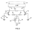
- the figure 3 shows an asymmetrical / symmetrical conversion differential amplifier as shown in FIG. figure 2 and further comprising, according to a main feature of the invention, a feedback circuit for equalizing the collector currents of the transistors.
- the circuit of feedback is a correction feedback impedance Zcorr connected between the collector C of the transistor T2 and the base b1 of the transistor T1.
- the principle used in the differential amplifier according to the invention consists in equalizing the collector currents i m , i p of the two transistors T1, T2 by compensation of the term ⁇ ⁇ v ⁇ 1 2 ⁇ zg .
- v ⁇ 1 2 ⁇ zg represents a local feedback from the base b1 of the transistor T1 to the collector C of the transistor T2 at the end ⁇ near ( ⁇ being very close to 1).
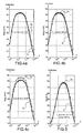
- the Figures 4a, 4b and 4b show the collector currents i m and ip of the transistors of the differential amplifier of the figure 2 , as a function of the impedance Zg of the current generator SC.
- the figure 4a shows the variation of the collector currents i m and ip as a function of the operating frequency F of the state-of-the-art differential amplifier, for an impedance Zg of the 100K ⁇ current generator.
- the superposition of the collector currents is respected up to a frequency F of 20 GHz.
- the capacitive effects of the transistors are particularly felt on the transistor T2, which has the effect of reducing its current gain ⁇ . So the term defining the ratio ⁇ ⁇ + 1 characterizing the probability of disappearance of an electron in the base of the transistor will be lower for T1 than for T2 resulting therefore a collector current i p lower than the collector current i m .
- the figure 4b shows the variation of the collector currents i m and ip as a function of the operating frequency F of the state-of-the-art differential amplifier for an impedance Zg of the current generator of 500 ⁇ .
- the differences of the collector currents are identical to those of the figure 4a at high frequency, but the difference is increasing between 1GHz and 20 GHz.
- the influence of the value of the impedance Zg of the current generator is thus directly more significant at intermediate frequencies between 1 GHz and 20 GHz.
- the figure 4c shows the variations of the collector currents i m and ip as a function of the operating frequency F of the differential amplifier of the state of the art for an impedance Zg of the even lower current generator of 100 ⁇ .
- the difference between the collector currents and thus the degradation of the performance of the differential amplifier is even more significant at intermediate frequencies.
- the correction feedback in the differential amplifier according to the invention makes it possible to compensate for a low impedance Zg of the order of 100 ⁇ of the current generator SC which represents the order of magnitude of the equivalent impedance of a mirror of current at these frequencies.
- a resistance Z corr 2 ⁇ 100 ⁇ , ie 200 ⁇ , is inserted between the base b1 of the transistor T1 and the collector C of the transistor T2.
- the collector currents i m and ip are almost confused as a function of the working frequency F compared to the currents of the collectors of the curves of the figure 4c , without compensation of the impedance Zg of the current generator, having a large dissymmetry.
- the differential asymmetrical / symmetrical conversion amplifier according to the invention is not limited to bipolar transistors T1, T2.
- MOSFET transistors can also be used to realize the amplifier with the corrective feedback Z corr .
- the sources are connected to the current generator SC, the drains being the symmetrical outputs of the amplifier.
- the counter-correction reaction by the resistance Z corr is then performed between the gate of transistor T1 and the drain of transistor T2.
- the new approach according to the invention thus makes it possible to dispense with the use of a passive type conversion device such as the BALUN which is accompanied by a degradation of the performances of the differential structure but also of a large implantation surface.
Landscapes
- Engineering & Computer Science (AREA)
- Power Engineering (AREA)
- Amplifiers (AREA)
Claims (4)
- Differentialverstärker zur asymmetrischen/symmetrischen Umwandlung, der einen Signal-v1-Eingang (b1) des asymmetrischen Typs in Bezug auf ein Referenzpotential (M) und einen Signalausgang (s1, s2) des symmetrischen Typs umfasst, wobei der Differentialverstärker zwei als gemeinsame Sender wirkende bipolare Transistoren T1, T2 umfasst, wobei die Sender E der beiden Transistoren T1, T2 durch zwei Rückkopplungsimpedanzen in Serie geschaltet sind, wobei ein perfekter Stromgenerator Ig und eine Impedanz Zg an den Anschlüssen des Stromgenerators Ig zwischen dem gemeinsamen Punkt der beiden Rückkopplungsimpedanzen und dem Referenzpotential geschaltet sind, wobei der Signal-v1-Eingang mit der Basis des Transistors T1 verbunden ist, wobei die Basis des Transistors T2 mit dem Referenzpotential verbunden ist, um mit der Basis des Transistors T1 den asymmetrischen Eingang zu bilden, wobei der symmetrische Ausgang von den Kollektoren der beiden Transistoren T1, T2 durch eine Impedanzanpassungsstufe CHBP des Ausgangs (s1, s2) realisiert wird,
dadurch gekennzeichnet, dass er eine Korrekturrückkopplungsimpedanz Zcorr aufweist, die zwischen dem Kollektor des Transistors T2 und der Basis des Transistors T1 geschaltet ist, um die Ströme der Kollektoren der beiden Transistoren T1, T2 symmetrisch zu machen, wobei der Wert der Korrekturrückkopplungsimpedanz Zcorr durch Zcorr = 2 Zg definiert wird. - Differentialverstärker nach Anspruch 1, dadurch gekennzeichnet, dass die beiden Transistoren T1, T2 entweder vom PNP-Typ oder vom NPN-Typ gewählt werden.
- Differentialverstärker nach Anspruch 4, dadurch gekennzeichnet, dass die Anpassungsstufe CHBP (10) vom Impedanzreduktionskaskodentyp ist.
- Differentialverstärker zur asymmetrischen/symmetrischen Umwandlung, der einen Signal-v1-Eingang (b1) des asymmetrischen Typs in Bezug auf ein Referenzpotential (M) und einen Signalausgang des symmetrischen Typs umfasst, wobei der Differentialverstärker zwei MOSFET-Transistoren T1, T2 als gemeinsame Sources umfasst, wobei die Sources der beiden Transistoren durch zwei Rückkopplungsimpedanzen in Serie geschaltet sind, wobei ein perfekter Stromgenerator Ig und eine Impedanz Zg an den Anschlüssen des Stromgenerators zwischen dem gemeinsamen Punkt der beiden Rückkopplungsimpedanzen und dem Referenzpotential geschaltet sind, wobei der Signal-v1-Eingang mit dem Gatter des Transistors T1 verbunden ist, wobei das Gatter des Transistors T2 mit dem Referenzpotential verbunden ist, um mit dem Gatter des Transistors T1 den asymmetrischen Eingang zu bilden, wobei der symmetrische Ausgang von den Drains der beiden Transistoren T1, T2 durch eine Impedanzanpassungsstufe CHBP des Ausgangs (s1, s2) realisiert wird,
dadurch gekennzeichnet, dass er eine Korrekturrückkopplungsimpedanz Zcorr umfasst, die zwischen dem Drain des Transistors T2 und der Basis des Transistors T1 geschaltet ist, um die Ströme der Drains der beiden Transistoren T1, T2 symmetrisch zu machen, wobei der Wert der Korrekturrückkopplungsimpedanz Zcorr durch Zcorr = 2 Zg definiert wird.
Applications Claiming Priority (1)
| Application Number | Priority Date | Filing Date | Title |
|---|---|---|---|
| FR1004820A FR2968860B1 (fr) | 2010-12-10 | 2010-12-10 | Amplicateur differentiel de conversion asymetrique/symetrique |
Publications (2)
| Publication Number | Publication Date |
|---|---|
| EP2464005A1 EP2464005A1 (de) | 2012-06-13 |
| EP2464005B1 true EP2464005B1 (de) | 2013-10-23 |
Family
ID=45023737
Family Applications (1)
| Application Number | Title | Priority Date | Filing Date |
|---|---|---|---|
| EP11191631.8A Active EP2464005B1 (de) | 2010-12-10 | 2011-12-01 | Differentialverstärker zur asymmetrischen/symmetrischen Umwandlung |
Country Status (3)
| Country | Link |
|---|---|
| US (1) | US8476981B2 (de) |
| EP (1) | EP2464005B1 (de) |
| FR (1) | FR2968860B1 (de) |
Families Citing this family (1)
| Publication number | Priority date | Publication date | Assignee | Title |
|---|---|---|---|---|
| US10027447B2 (en) * | 2016-10-17 | 2018-07-17 | Analog Devices, Inc. | Circuits for on-situ differential impedance balance error measurement and correction |
Family Cites Families (5)
| Publication number | Priority date | Publication date | Assignee | Title |
|---|---|---|---|---|
| SG81929A1 (en) * | 1998-06-01 | 2001-07-24 | Inst Of Microelectronics | Accurate and tuneable active differential phase splitters in rfic wireless applications |
| US6566961B2 (en) * | 2001-03-30 | 2003-05-20 | Institute Of Microelectronics | Wide-band single-ended to differential converter in CMOS technology |
| TWI269524B (en) * | 2004-11-08 | 2006-12-21 | Richwave Technology Corp | Low noise and high gain low noise amplifier |
| TW200937881A (en) * | 2008-02-21 | 2009-09-01 | Univ Nat Central | Wideband active balance converter of Darlington pair |
| TW201012056A (en) * | 2008-09-03 | 2010-03-16 | Novatek Microelectronics Corp | Active balun circuit |
-
2010
- 2010-12-10 FR FR1004820A patent/FR2968860B1/fr not_active Expired - Fee Related
-
2011
- 2011-12-01 EP EP11191631.8A patent/EP2464005B1/de active Active
- 2011-12-09 US US13/315,814 patent/US8476981B2/en active Active
Also Published As
| Publication number | Publication date |
|---|---|
| US20120313706A1 (en) | 2012-12-13 |
| US8476981B2 (en) | 2013-07-02 |
| FR2968860A1 (fr) | 2012-06-15 |
| FR2968860B1 (fr) | 2013-01-25 |
| EP2464005A1 (de) | 2012-06-13 |
Similar Documents
| Publication | Publication Date | Title |
|---|---|---|
| US8964898B2 (en) | Multi-function receiver with switched channelizer having high dynamic range active microwave filters using carbon nanotube electronics | |
| US12463595B2 (en) | Doherty power amplifier | |
| US9641143B2 (en) | Electronic device for a radiofrequency signal reception chain, comprising a low-noise transimpedance amplifier stage | |
| Vasilakopoulos et al. | A 92GHz bandwidth SiGe BiCMOS HBT TIA with less than 6dB noise figure | |
| US10896981B1 (en) | Integration of vertical GaN varactor with HEMT | |
| US8324966B2 (en) | Apparatus and methods for electronic amplification | |
| EP3681037A1 (de) | Elektronischer schaltkreis zur hüllkurvenerfassung, und entsprechender demodulator | |
| Takahashi et al. | 10-Gbit/s quadrature phase-shift-keying modulator and demodulator for 120-GHz-band wireless links | |
| Baeyens et al. | High gain-bandwidth differential distributed InP D-HBT driver amplifiers with large (11.3 V/sub pp/) output swing at 40 Gb/s | |
| WO2020203182A1 (ja) | 分布型回路 | |
| EP2464005A1 (de) | Differentialverstärker zur asymmetrischen/symmetrischen Umwandlung | |
| EP0318379A1 (de) | Ultrahochfrequenzverstärker mit sehr breitem Durchlassbereich | |
| EP0237099A1 (de) | Breitbandkettenverstärkerschaltung im Ultrahochfrequenzbereich | |
| Lischke et al. | Photonic BiCMOS technology—Enabler for Si-based, monolithically integrated transceivers towards 400 Gbps | |
| US8816766B2 (en) | Semiconductor integrated circuit, and reception apparatus and radio communication terminal including semiconductor integrated circuit | |
| Leoni et al. | A DC-45 GHz metamorphic HEMT traveling wave amplifier | |
| US9899966B2 (en) | Wideband high dynamic range low noise amplifier | |
| Weissbrodt et al. | Low-noise amplifiers in D-band using 100 nm and 50 nm mHEMT technology | |
| John et al. | Investigation of direct-coupled amplifier topologies for wireless communication systems using normally-on mHEMT technology | |
| Kim et al. | A DC-102GHz broadband amplifier in 0.12 µm SiGe BiCMOS | |
| Schick et al. | 40 Gbit/s differential distributed modulator driver realised in 80 GHz SiGe HBT process | |
| US20160204812A1 (en) | Direct envelope detection method of receiver from resonance antenna using maximum voltage transfer technique and receivers thereof | |
| Bavandi et al. | A Psuedo-Differential Transimpedance Amplifier with 36 GHz Bandwidth via Inductive Peaking in 22-nm FDSOI CMOS | |
| Sato et al. | 1.4-THz gain-bandwidth product InP-HEMTs preamplifier using an improved Cherry-Hooper topology | |
| Kumar et al. | A 12-GHz high output power amplifier using 0.18 µm SiGe BiCMOS for low power applications |
Legal Events
| Date | Code | Title | Description |
|---|---|---|---|
| PUAI | Public reference made under article 153(3) epc to a published international application that has entered the european phase |
Free format text: ORIGINAL CODE: 0009012 |
|
| AK | Designated contracting states |
Kind code of ref document: A1 Designated state(s): AL AT BE BG CH CY CZ DE DK EE ES FI FR GB GR HR HU IE IS IT LI LT LU LV MC MK MT NL NO PL PT RO RS SE SI SK SM TR |
|
| AX | Request for extension of the european patent |
Extension state: BA ME |
|
| 17P | Request for examination filed |
Effective date: 20121212 |
|
| GRAP | Despatch of communication of intention to grant a patent |
Free format text: ORIGINAL CODE: EPIDOSNIGR1 |
|
| INTG | Intention to grant announced |
Effective date: 20130522 |
|
| GRAS | Grant fee paid |
Free format text: ORIGINAL CODE: EPIDOSNIGR3 |
|
| GRAA | (expected) grant |
Free format text: ORIGINAL CODE: 0009210 |
|
| AK | Designated contracting states |
Kind code of ref document: B1 Designated state(s): AL AT BE BG CH CY CZ DE DK EE ES FI FR GB GR HR HU IE IS IT LI LT LU LV MC MK MT NL NO PL PT RO RS SE SI SK SM TR |
|
| REG | Reference to a national code |
Ref country code: GB Ref legal event code: FG4D Free format text: NOT ENGLISH |
|
| REG | Reference to a national code |
Ref country code: CH Ref legal event code: EP |
|
| REG | Reference to a national code |
Ref country code: AT Ref legal event code: REF Ref document number: 638034 Country of ref document: AT Kind code of ref document: T Effective date: 20131115 |
|
| REG | Reference to a national code |
Ref country code: IE Ref legal event code: FG4D Free format text: LANGUAGE OF EP DOCUMENT: FRENCH |
|
| REG | Reference to a national code |
Ref country code: DE Ref legal event code: R096 Ref document number: 602011003475 Country of ref document: DE Effective date: 20131219 |
|
| REG | Reference to a national code |
Ref country code: NL Ref legal event code: VDEP Effective date: 20131023 |
|
| REG | Reference to a national code |
Ref country code: AT Ref legal event code: MK05 Ref document number: 638034 Country of ref document: AT Kind code of ref document: T Effective date: 20131023 |
|
| REG | Reference to a national code |
Ref country code: LT Ref legal event code: MG4D |
|
| PG25 | Lapsed in a contracting state [announced via postgrant information from national office to epo] |
Ref country code: LT Free format text: LAPSE BECAUSE OF FAILURE TO SUBMIT A TRANSLATION OF THE DESCRIPTION OR TO PAY THE FEE WITHIN THE PRESCRIBED TIME-LIMIT Effective date: 20131023 Ref country code: FI Free format text: LAPSE BECAUSE OF FAILURE TO SUBMIT A TRANSLATION OF THE DESCRIPTION OR TO PAY THE FEE WITHIN THE PRESCRIBED TIME-LIMIT Effective date: 20131023 Ref country code: NO Free format text: LAPSE BECAUSE OF FAILURE TO SUBMIT A TRANSLATION OF THE DESCRIPTION OR TO PAY THE FEE WITHIN THE PRESCRIBED TIME-LIMIT Effective date: 20140123 Ref country code: NL Free format text: LAPSE BECAUSE OF FAILURE TO SUBMIT A TRANSLATION OF THE DESCRIPTION OR TO PAY THE FEE WITHIN THE PRESCRIBED TIME-LIMIT Effective date: 20131023 Ref country code: HR Free format text: LAPSE BECAUSE OF FAILURE TO SUBMIT A TRANSLATION OF THE DESCRIPTION OR TO PAY THE FEE WITHIN THE PRESCRIBED TIME-LIMIT Effective date: 20131023 Ref country code: IS Free format text: LAPSE BECAUSE OF FAILURE TO SUBMIT A TRANSLATION OF THE DESCRIPTION OR TO PAY THE FEE WITHIN THE PRESCRIBED TIME-LIMIT Effective date: 20140223 Ref country code: SE Free format text: LAPSE BECAUSE OF FAILURE TO SUBMIT A TRANSLATION OF THE DESCRIPTION OR TO PAY THE FEE WITHIN THE PRESCRIBED TIME-LIMIT Effective date: 20131023 |
|
| PG25 | Lapsed in a contracting state [announced via postgrant information from national office to epo] |
Ref country code: ES Free format text: LAPSE BECAUSE OF FAILURE TO SUBMIT A TRANSLATION OF THE DESCRIPTION OR TO PAY THE FEE WITHIN THE PRESCRIBED TIME-LIMIT Effective date: 20131023 Ref country code: CY Free format text: LAPSE BECAUSE OF FAILURE TO SUBMIT A TRANSLATION OF THE DESCRIPTION OR TO PAY THE FEE WITHIN THE PRESCRIBED TIME-LIMIT Effective date: 20131023 Ref country code: RS Free format text: LAPSE BECAUSE OF FAILURE TO SUBMIT A TRANSLATION OF THE DESCRIPTION OR TO PAY THE FEE WITHIN THE PRESCRIBED TIME-LIMIT Effective date: 20131023 Ref country code: AT Free format text: LAPSE BECAUSE OF FAILURE TO SUBMIT A TRANSLATION OF THE DESCRIPTION OR TO PAY THE FEE WITHIN THE PRESCRIBED TIME-LIMIT Effective date: 20131023 Ref country code: LV Free format text: LAPSE BECAUSE OF FAILURE TO SUBMIT A TRANSLATION OF THE DESCRIPTION OR TO PAY THE FEE WITHIN THE PRESCRIBED TIME-LIMIT Effective date: 20131023 |
|
| BERE | Be: lapsed |
Owner name: THALES Effective date: 20131231 |
|
| PG25 | Lapsed in a contracting state [announced via postgrant information from national office to epo] |
Ref country code: PT Free format text: LAPSE BECAUSE OF FAILURE TO SUBMIT A TRANSLATION OF THE DESCRIPTION OR TO PAY THE FEE WITHIN THE PRESCRIBED TIME-LIMIT Effective date: 20140224 |
|
| REG | Reference to a national code |
Ref country code: DE Ref legal event code: R097 Ref document number: 602011003475 Country of ref document: DE |
|
| PG25 | Lapsed in a contracting state [announced via postgrant information from national office to epo] |
Ref country code: EE Free format text: LAPSE BECAUSE OF FAILURE TO SUBMIT A TRANSLATION OF THE DESCRIPTION OR TO PAY THE FEE WITHIN THE PRESCRIBED TIME-LIMIT Effective date: 20131023 |
|
| PG25 | Lapsed in a contracting state [announced via postgrant information from national office to epo] |
Ref country code: RO Free format text: LAPSE BECAUSE OF FAILURE TO SUBMIT A TRANSLATION OF THE DESCRIPTION OR TO PAY THE FEE WITHIN THE PRESCRIBED TIME-LIMIT Effective date: 20131023 Ref country code: SK Free format text: LAPSE BECAUSE OF FAILURE TO SUBMIT A TRANSLATION OF THE DESCRIPTION OR TO PAY THE FEE WITHIN THE PRESCRIBED TIME-LIMIT Effective date: 20131023 Ref country code: LU Free format text: LAPSE BECAUSE OF FAILURE TO SUBMIT A TRANSLATION OF THE DESCRIPTION OR TO PAY THE FEE WITHIN THE PRESCRIBED TIME-LIMIT Effective date: 20131201 Ref country code: PL Free format text: LAPSE BECAUSE OF FAILURE TO SUBMIT A TRANSLATION OF THE DESCRIPTION OR TO PAY THE FEE WITHIN THE PRESCRIBED TIME-LIMIT Effective date: 20131023 Ref country code: CZ Free format text: LAPSE BECAUSE OF FAILURE TO SUBMIT A TRANSLATION OF THE DESCRIPTION OR TO PAY THE FEE WITHIN THE PRESCRIBED TIME-LIMIT Effective date: 20131023 |
|
| PLBE | No opposition filed within time limit |
Free format text: ORIGINAL CODE: 0009261 |
|
| STAA | Information on the status of an ep patent application or granted ep patent |
Free format text: STATUS: NO OPPOSITION FILED WITHIN TIME LIMIT |
|
| REG | Reference to a national code |
Ref country code: IE Ref legal event code: MM4A |
|
| PG25 | Lapsed in a contracting state [announced via postgrant information from national office to epo] |
Ref country code: DK Free format text: LAPSE BECAUSE OF FAILURE TO SUBMIT A TRANSLATION OF THE DESCRIPTION OR TO PAY THE FEE WITHIN THE PRESCRIBED TIME-LIMIT Effective date: 20131023 |
|
| 26N | No opposition filed |
Effective date: 20140724 |
|
| PG25 | Lapsed in a contracting state [announced via postgrant information from national office to epo] |
Ref country code: IE Free format text: LAPSE BECAUSE OF NON-PAYMENT OF DUE FEES Effective date: 20131201 Ref country code: BE Free format text: LAPSE BECAUSE OF NON-PAYMENT OF DUE FEES Effective date: 20131231 |
|
| REG | Reference to a national code |
Ref country code: DE Ref legal event code: R097 Ref document number: 602011003475 Country of ref document: DE Effective date: 20140724 |
|
| PG25 | Lapsed in a contracting state [announced via postgrant information from national office to epo] |
Ref country code: SI Free format text: LAPSE BECAUSE OF FAILURE TO SUBMIT A TRANSLATION OF THE DESCRIPTION OR TO PAY THE FEE WITHIN THE PRESCRIBED TIME-LIMIT Effective date: 20131023 |
|
| PG25 | Lapsed in a contracting state [announced via postgrant information from national office to epo] |
Ref country code: MC Free format text: LAPSE BECAUSE OF FAILURE TO SUBMIT A TRANSLATION OF THE DESCRIPTION OR TO PAY THE FEE WITHIN THE PRESCRIBED TIME-LIMIT Effective date: 20131023 |
|
| PG25 | Lapsed in a contracting state [announced via postgrant information from national office to epo] |
Ref country code: TR Free format text: LAPSE BECAUSE OF FAILURE TO SUBMIT A TRANSLATION OF THE DESCRIPTION OR TO PAY THE FEE WITHIN THE PRESCRIBED TIME-LIMIT Effective date: 20131023 Ref country code: SM Free format text: LAPSE BECAUSE OF FAILURE TO SUBMIT A TRANSLATION OF THE DESCRIPTION OR TO PAY THE FEE WITHIN THE PRESCRIBED TIME-LIMIT Effective date: 20131023 |
|
| PG25 | Lapsed in a contracting state [announced via postgrant information from national office to epo] |
Ref country code: BG Free format text: LAPSE BECAUSE OF FAILURE TO SUBMIT A TRANSLATION OF THE DESCRIPTION OR TO PAY THE FEE WITHIN THE PRESCRIBED TIME-LIMIT Effective date: 20131023 Ref country code: HU Free format text: LAPSE BECAUSE OF FAILURE TO SUBMIT A TRANSLATION OF THE DESCRIPTION OR TO PAY THE FEE WITHIN THE PRESCRIBED TIME-LIMIT; INVALID AB INITIO Effective date: 20111201 Ref country code: MK Free format text: LAPSE BECAUSE OF FAILURE TO SUBMIT A TRANSLATION OF THE DESCRIPTION OR TO PAY THE FEE WITHIN THE PRESCRIBED TIME-LIMIT Effective date: 20131023 |
|
| REG | Reference to a national code |
Ref country code: CH Ref legal event code: PL |
|
| PG25 | Lapsed in a contracting state [announced via postgrant information from national office to epo] |
Ref country code: MT Free format text: LAPSE BECAUSE OF FAILURE TO SUBMIT A TRANSLATION OF THE DESCRIPTION OR TO PAY THE FEE WITHIN THE PRESCRIBED TIME-LIMIT Effective date: 20131023 Ref country code: GR Free format text: LAPSE BECAUSE OF NON-PAYMENT OF DUE FEES Effective date: 20131023 |
|
| PG25 | Lapsed in a contracting state [announced via postgrant information from national office to epo] |
Ref country code: LI Free format text: LAPSE BECAUSE OF NON-PAYMENT OF DUE FEES Effective date: 20141231 Ref country code: CH Free format text: LAPSE BECAUSE OF NON-PAYMENT OF DUE FEES Effective date: 20141231 |
|
| REG | Reference to a national code |
Ref country code: FR Ref legal event code: PLFP Year of fee payment: 5 |
|
| PG25 | Lapsed in a contracting state [announced via postgrant information from national office to epo] |
Ref country code: GR Free format text: LAPSE BECAUSE OF FAILURE TO SUBMIT A TRANSLATION OF THE DESCRIPTION OR TO PAY THE FEE WITHIN THE PRESCRIBED TIME-LIMIT Effective date: 20140124 |
|
| REG | Reference to a national code |
Ref country code: FR Ref legal event code: PLFP Year of fee payment: 6 |
|
| REG | Reference to a national code |
Ref country code: FR Ref legal event code: PLFP Year of fee payment: 7 |
|
| PG25 | Lapsed in a contracting state [announced via postgrant information from national office to epo] |
Ref country code: AL Free format text: LAPSE BECAUSE OF FAILURE TO SUBMIT A TRANSLATION OF THE DESCRIPTION OR TO PAY THE FEE WITHIN THE PRESCRIBED TIME-LIMIT Effective date: 20131023 |
|
| P01 | Opt-out of the competence of the unified patent court (upc) registered |
Effective date: 20230427 |
|
| PGFP | Annual fee paid to national office [announced via postgrant information from national office to epo] |
Ref country code: DE Payment date: 20251119 Year of fee payment: 15 |
|
| PGFP | Annual fee paid to national office [announced via postgrant information from national office to epo] |
Ref country code: GB Payment date: 20251113 Year of fee payment: 15 |
|
| PGFP | Annual fee paid to national office [announced via postgrant information from national office to epo] |
Ref country code: IT Payment date: 20251126 Year of fee payment: 15 |
|
| PGFP | Annual fee paid to national office [announced via postgrant information from national office to epo] |
Ref country code: FR Payment date: 20251124 Year of fee payment: 15 |