EP2463967A2 - Interconnect member for an electronic module with embedded electrical components - Google Patents
Interconnect member for an electronic module with embedded electrical components Download PDFInfo
- Publication number
- EP2463967A2 EP2463967A2 EP11192420A EP11192420A EP2463967A2 EP 2463967 A2 EP2463967 A2 EP 2463967A2 EP 11192420 A EP11192420 A EP 11192420A EP 11192420 A EP11192420 A EP 11192420A EP 2463967 A2 EP2463967 A2 EP 2463967A2
- Authority
- EP
- European Patent Office
- Prior art keywords
- electrical
- module
- contacts
- circuit
- substrate
- Prior art date
- Legal status (The legal status is an assumption and is not a legal conclusion. Google has not performed a legal analysis and makes no representation as to the accuracy of the status listed.)
- Withdrawn
Links
- 239000000758 substrate Substances 0.000 claims abstract description 83
- 230000013011 mating Effects 0.000 claims abstract description 26
- 230000000903 blocking effect Effects 0.000 claims description 23
- 239000003990 capacitor Substances 0.000 claims description 21
- 230000005540 biological transmission Effects 0.000 claims description 10
- 229910000679 solder Inorganic materials 0.000 claims description 10
- 238000009499 grossing Methods 0.000 claims description 3
- 241000237519 Bivalvia Species 0.000 claims 1
- 235000020639 clam Nutrition 0.000 claims 1
- 230000008878 coupling Effects 0.000 description 11
- 238000010168 coupling process Methods 0.000 description 11
- 238000005859 coupling reaction Methods 0.000 description 11
- 239000000853 adhesive Substances 0.000 description 5
- 230000001070 adhesive effect Effects 0.000 description 5
- 239000000463 material Substances 0.000 description 3
- 229910010293 ceramic material Inorganic materials 0.000 description 2
- 239000004020 conductor Substances 0.000 description 2
- 239000011521 glass Substances 0.000 description 2
- 230000015654 memory Effects 0.000 description 2
- 238000000034 method Methods 0.000 description 2
- 230000008054 signal transmission Effects 0.000 description 2
- 239000004642 Polyimide Substances 0.000 description 1
- 238000003491 array Methods 0.000 description 1
- 230000000712 assembly Effects 0.000 description 1
- 238000000429 assembly Methods 0.000 description 1
- -1 but not limited to Polymers 0.000 description 1
- 239000000919 ceramic Substances 0.000 description 1
- 238000010276 construction Methods 0.000 description 1
- 239000007769 metal material Substances 0.000 description 1
- 230000003287 optical effect Effects 0.000 description 1
- 239000011368 organic material Substances 0.000 description 1
- 230000003071 parasitic effect Effects 0.000 description 1
- 239000004033 plastic Substances 0.000 description 1
- 229920003223 poly(pyromellitimide-1,4-diphenyl ether) Polymers 0.000 description 1
- 229920001721 polyimide Polymers 0.000 description 1
- 229920000642 polymer Polymers 0.000 description 1
- 230000000284 resting effect Effects 0.000 description 1
Images


Classifications
-
- H—ELECTRICITY
- H01—ELECTRIC ELEMENTS
- H01R—ELECTRICALLY-CONDUCTIVE CONNECTIONS; STRUCTURAL ASSOCIATIONS OF A PLURALITY OF MUTUALLY-INSULATED ELECTRICAL CONNECTING ELEMENTS; COUPLING DEVICES; CURRENT COLLECTORS
- H01R12/00—Structural associations of a plurality of mutually-insulated electrical connecting elements, specially adapted for printed circuits, e.g. printed circuit boards [PCB], flat or ribbon cables, or like generally planar structures, e.g. terminal strips, terminal blocks; Coupling devices specially adapted for printed circuits, flat or ribbon cables, or like generally planar structures; Terminals specially adapted for contact with, or insertion into, printed circuits, flat or ribbon cables, or like generally planar structures
- H01R12/70—Coupling devices
- H01R12/7076—Coupling devices for connection between PCB and component, e.g. display
-
- H—ELECTRICITY
- H01—ELECTRIC ELEMENTS
- H01R—ELECTRICALLY-CONDUCTIVE CONNECTIONS; STRUCTURAL ASSOCIATIONS OF A PLURALITY OF MUTUALLY-INSULATED ELECTRICAL CONNECTING ELEMENTS; COUPLING DEVICES; CURRENT COLLECTORS
- H01R13/00—Details of coupling devices of the kinds covered by groups H01R12/70 or H01R24/00 - H01R33/00
- H01R13/66—Structural association with built-in electrical component
-
- H—ELECTRICITY
- H01—ELECTRIC ELEMENTS
- H01R—ELECTRICALLY-CONDUCTIVE CONNECTIONS; STRUCTURAL ASSOCIATIONS OF A PLURALITY OF MUTUALLY-INSULATED ELECTRICAL CONNECTING ELEMENTS; COUPLING DEVICES; CURRENT COLLECTORS
- H01R12/00—Structural associations of a plurality of mutually-insulated electrical connecting elements, specially adapted for printed circuits, e.g. printed circuit boards [PCB], flat or ribbon cables, or like generally planar structures, e.g. terminal strips, terminal blocks; Coupling devices specially adapted for printed circuits, flat or ribbon cables, or like generally planar structures; Terminals specially adapted for contact with, or insertion into, printed circuits, flat or ribbon cables, or like generally planar structures
- H01R12/50—Fixed connections
- H01R12/51—Fixed connections for rigid printed circuits or like structures
- H01R12/55—Fixed connections for rigid printed circuits or like structures characterised by the terminals
- H01R12/58—Fixed connections for rigid printed circuits or like structures characterised by the terminals terminals for insertion into holes
- H01R12/585—Terminals having a press fit or a compliant portion and a shank passing through a hole in the printed circuit board
-
- H—ELECTRICITY
- H01—ELECTRIC ELEMENTS
- H01R—ELECTRICALLY-CONDUCTIVE CONNECTIONS; STRUCTURAL ASSOCIATIONS OF A PLURALITY OF MUTUALLY-INSULATED ELECTRICAL CONNECTING ELEMENTS; COUPLING DEVICES; CURRENT COLLECTORS
- H01R12/00—Structural associations of a plurality of mutually-insulated electrical connecting elements, specially adapted for printed circuits, e.g. printed circuit boards [PCB], flat or ribbon cables, or like generally planar structures, e.g. terminal strips, terminal blocks; Coupling devices specially adapted for printed circuits, flat or ribbon cables, or like generally planar structures; Terminals specially adapted for contact with, or insertion into, printed circuits, flat or ribbon cables, or like generally planar structures
- H01R12/70—Coupling devices
- H01R12/71—Coupling devices for rigid printing circuits or like structures
- H01R12/712—Coupling devices for rigid printing circuits or like structures co-operating with the surface of the printed circuit or with a coupling device exclusively provided on the surface of the printed circuit
- H01R12/716—Coupling device provided on the PCB
-
- H—ELECTRICITY
- H01—ELECTRIC ELEMENTS
- H01R—ELECTRICALLY-CONDUCTIVE CONNECTIONS; STRUCTURAL ASSOCIATIONS OF A PLURALITY OF MUTUALLY-INSULATED ELECTRICAL CONNECTING ELEMENTS; COUPLING DEVICES; CURRENT COLLECTORS
- H01R13/00—Details of coupling devices of the kinds covered by groups H01R12/70 or H01R24/00 - H01R33/00
- H01R13/02—Contact members
- H01R13/22—Contacts for co-operating by abutting
- H01R13/24—Contacts for co-operating by abutting resilient; resiliently-mounted
Definitions
- the invention relates to an interconnect member for electrically connecting an electronic module to a printed circuit.
- electronic modules have become more complex.
- electronic modules are being designed to switch more and more driver and receiver circuits at higher and higher speeds.
- Examples of electronic modules include chips, packages, processors, microprocessors, central processing units (CPUs), memories, integrated circuits, application specific integrated circuits (ASIC), and/or the like.
- Electronic modules are typically mounted on printed circuits (sometimes referred to as "circuit boards” or “printed circuit boards") within a larger, or host, electronic system.
- Electronic modules may suffer from unintended direct current (DC) coupling between the electronic module and other components of the larger system, such as another electronic module.
- DC direct current
- driver and receiver circuits of the electronic module and the other component may be unintentially DC coupled.
- Unintentional DC coupling can negatively impact electrical performance of the electronic system.
- unintentional DC coupling may generate noise along the signal paths of the electronic system.
- Unintentional DC coupling may be particularly troublesome for electronic systems that transmit high speed (e.g., above approximately 1 gigabits per second (Gbps)) differential signals.
- Gbps gigabits per second
- One technique for blocking DC coupling between the electronic module and other components of the electronic system includes positioning discrete DC blocking components (e.g., capacitors) within the signal paths of the printed circuit on which the electronic module is mounted.
- discrete DC blocking components e.g., capacitors
- only a limited amount of space is available on the printed circuit on which the electronic module is mounted.
- printed circuits may not have room for discrete DC blocking components.
- adding discrete DC blocking components within the signal paths of the printed circuit may negatively impact the electrical performance of the printed circuit.
- the DC blocking components may necessitate a less than optimal relative arrangement of the various signal paths along the printed circuit, which may add noise and/or reduce signal transmission rates along the signal paths.
- parasitic inductance, capacitance, resistance, and/or the like of the discrete DC blocking components may also negatively impact the electrical performance of the printed circuit on which the electronic module is mounted.
- Another technique for blocking DC coupling between an electronic module and other components of a larger electronic system includes positioning discrete DC blocking components within an electrical connector that electrically connects the printed circuit on which the electronic module is mounted to the other component. But, DC blocking components located within such electrical connectors may not be close enough to the electronic module to be effective to block DC coupling between the electronic module and the other components of the larger system.
- an interconnect member for electrically connecting an electronic module to a printed circuit comprises a substrate having a module side and an opposite circuit side.
- Module contacts are arranged in an array along the module side of the substrate and comprise module mating interfaces that are configured to be electrically connected to the electronic module.
- Circuit contacts are arranged in an array along the circuit side of the substrate and comprise circuit mating interfaces that are configured to be electrically connected to the printed circuit.
- Electrical components extend between and electrically connect corresponding module contacts to corresponding circuit contacts to provide electrical paths for electrical signals transmitted between the module contacts and the circuit contacts. The electrical components modify the corresponding electrical signals transmitted along the electrical paths between the corresponding module contacts and circuit contacts.
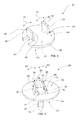
- Figure 1 is a partially exploded perspective view of an exemplary embodiment of an electronic module assembly.
- Figure 2 is a cross-sectional view of a portion of an exemplary embodiment of an interconnect member of the electronic module assembly shown in Figure 1 .
- Figure 3 is a perspective view of an exemplary embodiment of an electrical contact of the interconnect member shown in Figure 2 .
- Figure 4 is a perspective view of an exemplary embodiment of another electrical contact of the interconnect member shown in Figure 2 .
- Figure 5 is a cross-sectional view of a portion of the electronic module assembly shown in Figure 1 .
- Figure 6 is a cross-sectional view of a portion of an exemplary alternative embodiment of an interconnect member.
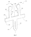
- Figure 7 is a perspective view of an exemplary alternative embodiment of an electrical contact of the interconnect member shown in Figure 2 .
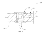
- Figure 8 is a cross-sectional view of a portion of another exemplary alternative embodiment of an interconnect member.
- FIG. 1 is a partially exploded perspective view of an exemplary embodiment of an electronic module assembly 10.
- the electronic module assembly 10 includes an electrical connector 12, a printed circuit 14, and an electronic module 16.
- the electrical connector 12 is mounted on the printed circuit 14.
- the electronic module 16 is loaded onto the electrical connector 12 to electrically connect the electronic module 16 to the printed circuit 14 via the electrical connector 12.
- the electrical connector 12 is a socket connector.
- the electronic module 16 may be any type of electronic module, such as, but not limited to, a chip, a package, a processor, a microprocessor, a central processing unit (CPU), a memory, an integrated circuit, an application specific integrated circuit (ASIC), and/or the like.
- the electrical connector 12 includes a dielectric alignment frame 18 that is mounted on the printed circuit 14.
- the alignment frame 18 is a component of an interconnect member 20 that includes an array of electrical contacts 22 and an array of electrical contacts 24 ( Figures 2 , 4 , and 5 ).
- the electronic module 16 has a mating side 26 along which the electronic module 16 mates with the interconnect member 20.
- the interconnect member 20 is interposed between contact pads 28 ( Figure 5 ) on the mating side 26 of the electronic module 16 and corresponding electrical vias 30 ( Figure 5 ) of the printed circuit 14 to electrically connect the electronic module 16 to the printed circuit 14.
- the electrical contacts 22 may be referred to herein as "module contacts”
- the electrical contacts 24 may be referred to herein as "circuit contacts”.
- the contact pads 28 may be referred to herein as "electrical contacts”.
- FIG 2 is a cross-sectional view of a portion of an exemplary embodiment of the interconnect member 20.
- the interconnect member 20 includes a dielectric substrate 32 that holds the electrical contacts 22 and 24.
- the substrate 32 includes a module side 34 and an opposite circuit side 36.
- the electrical contacts 22 are arranged in an array along the module side 34 of the substrate 32 for electrical connection to the electronic module 16 ( Figures 1 and 5 ).
- Each electrical contact 22 includes a mating interface 38 that is configured to be electrically connected to a corresponding one of the contact pads 28 ( Figure 5 ) on the mating side 26 ( Figures 1 and 5 ) of the electronic module 16.
- the array of electrical contacts 22 may include any number of electrical contacts 22 overall and the contacts 22 may be arranged in any pattern having any number of rows and columns. The pattern of the array of electrical contacts 22 shown in Figure 1 is meant as exemplary only.
- the mating interfaces 38 may be referred to herein as "module mating interfaces”.
- the electrical contacts 24 are arranged in an array along the circuit side 36 of the substrate 32 for electrical connection to the printed circuit 14 ( Figures 1 and 5 ).
- the electrical contacts 24 include mating interfaces 40 that are configured to be electrically connected to corresponding electrical vias 30 ( Figure 5 ) of the printed circuit 14.
- the array of electrical contacts 24 may include any number of electrical contacts 24 overall and the contacts 24 may be arranged in any pattern having any number of rows and columns.
- the mating interfaces 40 may be referred to herein as "circuit mating interfaces".
- the substrate 32 includes an array of openings 42 that extend through the substrate 32. More particularly, the openings 42 extend through both of the module and circuit sides 34 and 36, respectively, and completely through the substrate 32 between the sides 34 and 36.
- the array of openings 42 is aligned with the arrays of the electrical contacts 22 and 24 such that the electrical contacts 22 are aligned with corresponding openings 42 on the module side 34 of the substrate 32 and the electrical contacts 24 are aligned with corresponding openings 42 on the circuit side 36.
- the interconnect member 20 includes a plurality of electrical components 44. Each electrical component 44 is held within a corresponding opening 42 and is electrically connected to the corresponding electrical contacts 22 and 24. Within the corresponding opening 42, the electrical component 44 extends between and electrically connects the corresponding electrical contacts 22 and 24 together. Each electrical component 44 thereby provides an electrical path through the substrate 32 for electrical signals transmitted between the corresponding electrical contacts 22 and 24. Each electrical signal transmitted between corresponding contacts 22 and 24 may be a data signal, electrical power, and/or the like.
- Each of the electrical components 44 modifies the corresponding electrical signal that is transmitted along the electrical path defined by the electrical component 44 between the corresponding electrical contacts 22 and 24.
- modifying the corresponding electrical signal is intended to mean any functionality of the electrical component 44 that is performed by the electrical component 44 in addition to providing the electrical path between the corresponding electrical contacts 22 and 24.
- the electrical components 44 modify the corresponding electrical signals by providing one or more different (with respect to the transmission) functionalities relative to the corresponding electrical signals.
- Each electrical component 44 may modify the corresponding electrical signal in any manner, fashion, way, and/or the like.
- each electrical component 44 may modify the corresponding electrical signal by blocking direct current (DC) in at least one direction along the electrical path between the corresponding electrical contacts 22 and 24, by switching the electrical path between the corresponding electrical contacts 22 and 24 between an open and closed state, by amplifying the corresponding electrical signal, and/or the like.
- DC direct current
- Other examples of modifying the corresponding electrical signal include smoothing an output of the corresponding electrical signal, storing electrical energy of the corresponding electrical signal, limiting the flow of electrical current of the corresponding electrical signal, and/or the like.
- Still more examples of modifying the corresponding electrical signal include blocking transmission of the corresponding electrical signal in one direction along the electrical path between the corresponding electrical contacts 22 and 24, converting the corresponding electrical signal into a different form of energy, and/or the like.
- the electrical components 44 include DC blocking components that facilitate blocking DC coupling between the electronic module 16 and another component (not shown) within a larger, or host, electronic system (not shown) that includes the electronic module assembly 10.
- the electrical components 44 may each include any type of electrical component that modifies the corresponding electrical signal in any manner, fashion, way, and/or the like.
- Examples of the electrical components 44 include, but are not limited to, capacitors, resistors, diodes, transistors, transducers, switches, active electrical components, passive electrical components, and/or the like.
- one or more of the electrical components 44 may include a capacitor for, for example, blocking direct current (DC) in at least one direction along the electrical path between the corresponding electrical contacts 22 and 24, for smoothing an output of the corresponding electrical signal, for storing electrical energy of the corresponding electrical signal, and/or the like.
- DC direct current
- one or more of the electrical components 44 may include a resistor for, for example, limiting the flow of electrical current of the corresponding electrical signal, and/or the like.
- One or more of the electrical components 44 may include a diode for, for example, blocking transmission of the corresponding electrical signal in one direction along the electrical path between the corresponding electrical contacts 22 and 24, and/or the like.
- Other examples include embodiments wherein one or more of the electrical components 44 may include a transistor for, for example, switching the electrical path between the corresponding electrical contacts 22 and 24 between an open and closed state, for amplifying the corresponding electrical signal, and/or the like.
- one or more of the electrical components 44 includes a switch for, for example, switching the electrical path between the corresponding electrical contacts 22 and 24 between an open and closed state, and/or the like.
- one or more of the electrical components 44 may include a transducer for, for example, converting the corresponding electrical signal into a different form of energy, and/or the like.
- the electrical signal may be converted into any other form of energy, such as, but not limited to, electro-mechanical energy, electromagnetic energy, photonic energy, optical energy, photovoltaic energy, and/or the like.
- the electrical component 44 may be used as a sensor, detector, and/or the like.
- each of the electrical components 44 includes a DC blocking component that facilitates blocking DC coupling.
- the electrical components 44 block DC from being transmitted in at least one direction along the electrical paths between the electrical contacts 22 and 24.
- the electrical components 44 may each include any component that is configured to facilitate blocking DC.
- the electrical components 44 include capacitors that may each be any type of capacitor having any overall construction. Examples of capacitors that may be used as a DC blocking component include, but are not limited to, parallel plate capacitors, fixed capacitors, variable capacitors, gimmick capacitors, trimmer capacitors, electrolytic capacitors, printed circuit board capacitors, integrated circuit capacitors, vacuum capacitors, an active capacitor, a passive capacitor, and/or the like.
- one or more of the electrical components 44 may include any other type of component that is configured to facilitate blocking DC, such as, but not limited to, a resistor, a diode, an active component, a passive component, and/or the like.
- Each electrical component 44 includes a body 46 that extends a length from a module end 48 to a circuit end 50.
- the body 46 has the shape of a parallelepiped.
- the exemplary embodiment of the body 46 of each electrical component 44 has a rectangular cross-sectional shape.
- the body 46 of each electrical component 44 may additionally or alternatively include any other shape.
- the electrical components 44 include a cap 52 on the module end 48 and/or a cap 54 on the circuit end 50 of the body 46.
- the caps 52 and/or 54 are optionally formed from different materials from the body 46.
- the caps 52 and 54 of one or more of the electrical components 44 are formed from a metallic material, and the body 46 is formed from a ceramic material.
- the caps 52 and 54 and the body 46 may each include any other material.
- the cap 52 may be referred to herein as a "module cap”, while the cap 54 may be referred to herein as a "circuit cap”.
- FIG 3 is a perspective view of an exemplary embodiment of one of the electrical contacts 22.
- the electrical contact 22 includes a mounting base 56 and fingers 58 that extend outwardly from the mounting base 56.
- the mounting base 56 has a substrate side 60 and an opposite module side 62.
- the module side 62 includes the mating interface 38 of the electrical contact 22.
- the mounting base 56 is configured to be mechanically connected to the substrate 32 on the module side 34 of the substrate 32.
- the mounting base 56 is optionally sized such that a portion of the mounting base 56 extends over the module side 34 of the substrate 32 around the corresponding opening 42 ( Figures 2 and 5 ).
- the fingers 58 extend outwardly from the substrate side 60 of the mounting base 56. Each finger 58 extends a length from an end 64 that is connected to the mounting base 56 to a free end 66.
- the fingers 58 oppose each other. More particularly, each finger 58 includes a gripping surface 68 that faces the gripping surface 68 of the other finger 58.
- the fingers 58 are springs such that the free end 66 of each finger 58 is resiliently deflectable along a corresponding arc 70.
- the position of each finger 58 shown in Figure 3 is the natural resting, or undeflected, position of the finger 58.
- each electrical contact 22 may include any number of the fingers 58.
- the substrate 32 includes an array of metallic pads 72 that are used to mount the mounting bases 56 of the electrical contacts 22 on the substrate 32.
- the array of pads 72 is aligned with the array of openings 42 such that the pads 72 extend around corresponding openings 42 on the module side 34 of the substrate 32.
- the mounting base 56 of each electrical contact 22 is soldered to the corresponding pad 72 to mechanically connect the mounting base 56, and thus the electrical contacts 22, to the module side 34 of the substrate 32.
- the mounting base 56 of one or more of the electrical contacts 22 is mechanically connected to the corresponding pad 72 (which may or may not be metallic) on the module side 34 of the substrate 32 using an adhesive, using a press-fit (or interference) connection, using a snap-fit connection, and/or using another type of mechanical fastener, connection, and/or the like.
- the mounting base 56 of one or more of the electrical contacts 22 may be mechanically connected directly to the surface of the substrate 32 that defines the module side 34, such as, but not limited to, using an adhesive, using a press-fit (or interference) connection, using a snap-fit connection, and/or using another type of mechanical fastener, connection, and/or the like.
- the fingers 58 When the mounting base 56 of an electrical contact 22 is mechanically connected to the substrate 32 as shown in Figure 2 , the fingers 58 extend into the corresponding opening 42. The fingers 58 engage the corresponding electrical component 44 to hold a portion of the electrical component 44 therebetween. More particularly, the gripping surfaces 68 of the fingers 58 engage the cap 52 of the corresponding electrical component 44 such that the cap 52 is held between the fingers 58. The engagement between the gripping surfaces 68 of the fingers 58 and the cap 52 mechanically and electrically connects the electrical contact 22 to the cap 52 and thereby to the corresponding electrical component 44. In the exemplary embodiment, the mechanical connection between the fingers 58 and the cap 52 is created by an interference fit between the fingers 58 and the cap 52.
- the cap 52 deflects the free ends 66 of the fingers 58 from the undeflected positions in directions away from each other.
- the gripping surfaces 68 of the fingers 58 are soldered to the cap 52.
- each electrical component 44 may be mechanically and/or electrically connected to the corresponding electrical contact 22 using any other structure, means, connection type, and/or the like, such as, but not limited to, using an adhesive and/or using another type of mechanical fastener, connection, and/or the like.
- the mating interfaces 38 of the electrical contacts 22 are contact pads that are configured to engage solder balls 74 ( Figure 5 ) that engage the contact pads 28 ( Figure 5 ) on the mating side 26 ( Figures 1 and 5 ) of the electronic module 16.
- the solder balls 74 provide an electrical connection between the mating interfaces 38 of the electrical contacts 22 and the contact pads 28 of the electronic module 16.
- the mating interface 38 of one or more of the electrical contacts 22 directly engages the corresponding contact pad 28 of the electronic module 16.
- the mating interface 3 8 of one or more of the electrical contacts 22 may include another type of contact, such as, but not limited to, a solder tail, a pin that is configured to be press-fit into the electronic module 16 and/or an intervening structure, and/or the like.
- FIG 4 is a perspective view of an exemplary embodiment of one of the electrical contacts 24.
- the electrical contact 24 includes a base 76 having a substrate side 80 and an opposite circuit side 82. Fingers 78 extend outwardly from the base 76.
- a pin 84 extends outwardly from the circuit side 82 of the base 76.
- the pin 84 includes the mating interface 40 of the electrical contact 24.
- the electrical contact 24 is configured to be mechanically connected to the substrate 32 ( Figures 2 and 5 ).
- the electrical contact 24 includes optional barbs 86 that extend outwardly from outer sides 88 of the fingers 78. The barbs 86 facilitate mechanically connecting the electrical contact 24 to the substrate 32 with an interference fit, as will be described below.
- the base 76 is sized such that a portion of the base 76 extends over the circuit side 36 ( Figures 2 and 5 ) of the substrate 32 around the corresponding opening 42 ( Figures 2 and 5 ).
- the electrical contact 24 may include any number of the barbs 86.
- the fingers 78 extend outwardly from the substrate side 80 of the base 76. Each finger 78 extends outwardly to a free end 90.
- the fingers 78 oppose each other in that the fingers 78 include inner sides 92 that face each other.
- the fingers 78 are springs such that the free end 90 of each finger 78 is resiliently deflectable along a corresponding arc 94.
- the position of each finger 78 shown in Figure 4 is the undeflected position of the finger 78. When deflected along the corresponding arc 94 in either direction therealong, the finger 78 experiences a biasing force that acts along the arc 94 in the opposite direction to the direction of deflection to bias the finger 78 toward the undeflected position.
- the inner sides 92 of the fingers 78 optionally include barbs 96 that engage the corresponding electrical component 44 ( Figures 2 and 5 ) to mechanically and electrically connect the electrical contact 24 to the corresponding electrical component 44, as will be described below. Although two fingers 78 are shown, each electrical contact 24 may include any number of the fingers 78.
- the pin 84 of each electrical contact 24 is configured to be press-fit into a corresponding one of the electrical vias 30 ( Figure 5 ) of the printed circuit 14 ( Figures 1 and 5 ). Engagement between the pins 84 and the conductive materials of the electrical vias 30 provides an electrical connection between the electrical contacts 24 and the electrical vias 30 of the printed circuit 14.
- the pins 84 are Micro ACTION PIN® (MAP) contacts.
- one or more of the electrical contacts 24 includes another type of press-fit pin, such as, but not limited to, an eye-of-the needle pin and/or the like.
- other types of contacts besides press-fit pins may be used in alternative embodiments for electrically connecting one or more of the electrical contacts 24 to the printed circuit 14, such as, but not limited to, surface mount contacts, solder tails, and/or the like.
- each electrical contact 24 is mechanically connected to the substrate 32 using an interference fit. More particularly, the barbs 86 of each electrical contact 24 engage the substrate 32 within the corresponding opening 42 with an interference fit to hold the electrical contact 24 to the substrate 32. In addition or alternatively to the barbs 86 and/or the interference fit, one or more of the electrical contacts 24 may be mechanically connected to the substrate 32 using an adhesive, using a snap-fit connection, and/or using another type of mechanical fastener, connection, and/or the like.
- the fingers 78 When an electrical contact 24 is mechanically connected to the substrate 32 as shown in Figure 2 , the fingers 78 extend into the corresponding opening 42 and engage the corresponding electrical component 44 to hold a portion of the electrical component 44 therebetween. More particularly, the barbs 96 of the fingers 78 engage the cap 54 of the corresponding electrical component 44 such that the cap 54 is held between the fingers 78. Engagement between the barbs 96 of the fingers 78 and the cap 54 mechanically and electrically connects the electrical contact 24 to the cap 54 and thereby to the corresponding electrical component 44.
- the mechanical connection between the fingers 78 and the cap 54 is created by an interference fit between the fingers 78 and the cap 54.
- the cap 54 deflects the free ends 90 of the fingers 78 from the undeflected positions in directions away from each other.
- the barbs 96 of the fingers 58 are soldered to the cap 54.
- each electrical component 44 may be mechanically and/or electrically connected to the corresponding electrical contact 24 using any other structure, means, connection type, and/or the like, such as, but not limited to, using an adhesive and/or using another type of mechanical fastener, connection, and/or the like.
- Figure 5 is a cross-sectional view of a portion of the electronic module assembly 10.
- the pins 84 of the electrical contacts 24 are received within the corresponding electrical vias 30 of the printed circuit 14.
- the pins 84 are engaged with the conductive materials of the electrical vias 30 such that the pins 84 are electrically connected to corresponding traces 98 of the printed circuit 14.
- the traces 98 are shown in Figure 5 as being internal traces of the printed circuit 14, alternatively the corresponding electrical trace 98 of one or more of the pins 84 is located on an exterior surface of the printed circuit 14.
- the electrical vias 30 are back-drilled as shown in Figure 5 , for example to facilitate preventing electrical stubs.
- the bases 76 of the electrical contacts 24 are optionally sized such that a portion of the base 76 extends over the circuit side 36 of the substrate 32 around the corresponding opening 42. Accordingly, if a force is applied to the interconnect member 20 and/or the electronic module 16 to press the pins 84 into the electrical vias 30, such a force is transmitted to the pins 84 through the base 76 via the engagement of the circuit side 36 of the substrate 32 with the base 76, instead of through the electrical components 44.
- the bases 76 of the electrical contacts 24 may thereby facilitate preventing damage to the electrical components 44 as the pins 84 are pressed into the electrical vias 30.
- the electrical contacts 24 are mechanically connected to the substrate 32 via the interference fit between the barbs 86 and the substrate 32.
- the fingers 78 of the electrical contacts 24 hold the caps 54 of the corresponding electrical components 44 such that the electrical components 44 are electrically and mechanically connected to the corresponding electrical contacts 24.
- the fingers 58 of the electrical contacts 22 hold the caps 52 of the corresponding electrical components 44.
- the electrical components 44 are thereby electrically and mechanically connected to the corresponding electrical contacts 22.
- the bases 56 of the electrical contacts 22 are mechanically connected to the substrate 32 via the solder connection between the bases 56 and the corresponding pads 72.
- the mating interfaces 38 of the electrical contacts 22 are engaged with the corresponding solder balls 74, which are engaged with the corresponding contact pads 28 on the mating side 26 of the electronic module 16.
- the electrical contacts 22 are thereby electrically connected to the corresponding contact pads 28 of the electronic module 16.
- the electrical components 44 extend between and electrically connect the corresponding electrical contacts 22 and 24 together. Each electrical component 44 provides an electrical path through the substrate 32 for electrical signals transmitted between the corresponding electrical contacts 22 and 24. Accordingly, the contact pads 28 on the electronic module 16 are electrically connected to the corresponding traces 98 of the printed circuit 14. The interconnect member 20 thereby electrically connects the electronic module 16 to the printed circuit 14. In the exemplary embodiment of the electrical components 44, the electrical components 44 block DC from being transmitted in at least one direction along the electrical paths between the electrical contacts 22 and 24. The electrical components 44 thereby facilitate blocking DC coupling between the electronic module 16 and another component (not shown) within a larger, or host, electronic system (not shown) that includes the electronic module assembly 10.
- an electrical component 44 When an electrical component 44 includes a capacitor, the capacitive value of the capacitor is optionally selected based at least on a data transmission rate of data signals that are conveyed along the electrical path of the electrical component 44. Similarly, when an electrical component 44 includes a resistor and/or a diode, the resistance value of the resistor and/or the value of the diode is optionally selected based at least on a data transmission rate of data signals that are conveyed along the electrical path of the electrical component 44.
- FIG 6 is a cross-sectional view of a portion of an exemplary alternative embodiment of an interconnect member 120.
- the interconnect member 120 includes a dielectric substrate 132 that holds an array of electrical contacts 122 and an array of electrical contacts 124.
- the substrate 132 includes a module side 134 and an opposite circuit side 136.
- the electrical contacts 122 are arranged within the array along the module side 134 of the substrate 132 for electrical connection to the electronic module 16 ( Figures 1 and 5 ).
- the electrical contacts 124 are arranged within the array along the circuit side 136 of the substrate 132 for electrical connection to the printed circuit 14 ( Figures 1 and 5 ).
- the electrical contacts 122 may be referred to herein as "module contacts", while the electrical contacts 124 may be referred to herein as "circuit contacts”.
- the substrate 132 includes an array of openings 142 that extend through the substrate 132.
- the interconnect member 120 includes a plurality of electrical components 144. Each electrical component 144 is held within a corresponding opening 142 and is electrically connected to the corresponding electrical contacts 122 and 124. Within the corresponding opening 142, the electrical component 144 extends between and electrically connects the corresponding electrical contacts 122 and 124 together. Each electrical component 144 thereby provides an electrical path through the substrate 132 for electrical signals transmitted between the corresponding electrical contacts 122 and 124.
- the electrical components 144 include diodes that block transmission of the corresponding electrical signals in one direction along the electrical paths between the electrical contacts 122 and 124.
- Each of the diodes may block transmission of the corresponding electrical signal in either direction along the electrical path between the corresponding electrical contacts 122 and 124.
- the value of each diode is optionally selected based at least on a data transmission rate of data signals that are conveyed along the electrical path of the electrical component 144.
- the electrical contacts 122 include bases 156.
- the bases 156 of the electrical contacts 122 do not extend over the module side 134 of the substrate 132 around the corresponding opening 142.
- the bases 156 can float along a float axis 200. The floating ability of the bases 156 of the electrical contacts 122 may facilitate preventing damage to the electrical components 144, the electrical contacts 122, the electrical contacts 124, and/or other components of the interconnect member 120 caused by different coefficients of thermal expansion of the various components of the interconnect member 120.
- the various components of the interconnect member 120 may expand and/or contract at different rates, which may damage components (and/or the connections therebetween) that are rigidly connected together.
- FIG 7 is a perspective view of an exemplary alternative embodiment of an electrical contact 224, which may be used in place of an electrical contact 24 ( Figures 2 , 4 , and 5 ) or an electrical contact 124 ( Figures 6 ).
- the electrical contact 224 includes a base 276 having a substrate side 280 and an opposite circuit side 282. Fingers 278 extend outwardly from the base 276.
- a pin 284 extends outwardly from the circuit side 282 of the base 276.
- the pin 284 includes a mating interface 240 of the electrical contact 224.
- the electrical contact 224 is configured to be mechanically connected to the substrate 32 ( Figures 2 and 5 ).
- the electrical contact 224 includes one or more barbs (not shown) to facilitate mechanically connecting the electrical contact 224 to the substrate 32 with an interference fit.
- the base 276 is optionally sized such that a portion of the base 276 extends over the circuit side 36 ( Figures 2 and 5 ) of the substrate 32 around the corresponding opening 42 ( Figures 2 and 5 ).
- the fingers 278 extend outwardly from the substrate side 280 of the base 276. Each finger 278 extends outwardly to a free end 290.
- the fingers 278 oppose each other in that the fingers 278 include inner sides 292 that face each other.
- the fingers 278 are springs such that the free end 290 of each finger 278 is resiliently deflectable along a corresponding arc 294.
- the position of each finger 278 shown in Figure 7 is the undeflected position of the finger 278. When deflected along the corresponding arc 294 in either direction therealong, the finger 278 experiences a biasing force that acts along the arc 294 in the opposite direction to the direction of deflection to bias the finger 278 toward the undeflected position.
- the inner sides 292 of the fingers 278 optionally include barbs 296 that engage the corresponding electrical component 44 ( Figures 2 and 5 ) to mechanically and electrically connect the electrical contact 24 to the corresponding electrical component 44.
- each electrical contact 224 may include any number of the fingers 278.
- FIG 8 is a cross-sectional view of a portion of an exemplary alternative embodiment of an interconnect member 320.
- the interconnect member 320 includes a dielectric substrate 332 that holds an array of electrical contacts 322 and an array of electrical contacts 324.
- the substrate 332 includes a module side 334 and an opposite circuit side 336.
- the electrical contacts 322 are arranged within the array along the module side 334 of the substrate 332 for electrical connection to the electronic module 16 ( Figures 1 and 5 ).
- the electrical contacts 324 are arranged within the array along the circuit side 336 of the substrate 332 for electrical connection to the printed circuit 14 ( Figures 1 and 5 ).
- the electrical contacts 322 may be referred to herein as "module contacts", while the electrical contacts 324 may be referred to herein as "circuit contacts”.
- the substrate 332 includes an array of openings 342 that extend through the substrate 332.
- the interconnect member 320 includes a plurality of electrical components 344. Each electrical component 344 is held within a corresponding opening 342 and is electrically connected to the corresponding electrical contacts 322 and 324. Within the corresponding opening 342, the electrical component 344 extends between and electrically connects the corresponding electrical contacts 322 and 324 together. Each electrical component 344 thereby provides an electrical path through the substrate 332 for electrical signals transmitted between the corresponding electrical contacts 322 and 324.
- the electrical components 344 include resistors that limit the flow of electrical current along the electrical paths between the electrical contacts 322 and 324. In other words, the resistors limit the flow of the corresponding electrical signal. The resistance value of each resistor is optionally selected based at least on a data transmission rate of data signals that are conveyed along the electrical path of the electrical component 344.
- inventions described and/or illustrated herein may provide an electrical module assembly having electrical components that are located closer to the electronic module than at least some known electronic module assemblies.
- a substrate of the printed circuit 14 may be a flexible substrate or a rigid substrate.
- the substrate may be fabricated from and/or include any material(s), such as, but not limited to, ceramic, epoxy-glass, polyimide (such as, but not limited to, Kapton® and/or the like), organic material, plastic, polymer, and/or the like.
- the substrate is a rigid substrate fabricated from epoxy-glass, such that the printed circuit 14 is what is sometimes referred to as a "circuit board” or a "printed circuit board”.
Landscapes
- Coupling Device And Connection With Printed Circuit (AREA)
- Structures For Mounting Electric Components On Printed Circuit Boards (AREA)
Abstract
An interconnect member (20) for electrically connecting an electronic module to a printed circuit comprises a substrate (32) having a module side (34) and an opposite circuit side (36). Module contacts (22) are arranged in an array along the module side (34) of the substrate (32) and comprise module mating interfaces (38) that are configured to be electrically connected to the electronic module. Circuit contacts (24) are arranged in an array along the circuit side (36) of the substrate (32) and comprise circuit mating interfaces (40) that are configured to be electrically connected to the printed circuit. Electrical components (44) extend between and electrically connect corresponding module contacts (22) to corresponding circuit contacts (24) to provide electrical paths for electrical signals transmitted between the module contacts (22) and the circuit contacts (24). The electrical components (44) modify the corresponding electrical signals transmitted along the electrical paths between the corresponding module contacts (22) and circuit contacts (24).
Description
- The invention relates to an interconnect member for electrically connecting an electronic module to a printed circuit.
- Competition and market demands have continued the trend toward smaller and higher performance (e.g., faster) electronic systems. To achieve such reduced sized and higher performance systems, electronic modules have become more complex. For example, electronic modules are being designed to switch more and more driver and receiver circuits at higher and higher speeds. Examples of electronic modules include chips, packages, processors, microprocessors, central processing units (CPUs), memories, integrated circuits, application specific integrated circuits (ASIC), and/or the like. Electronic modules are typically mounted on printed circuits (sometimes referred to as "circuit boards" or "printed circuit boards") within a larger, or host, electronic system.
- Electronic modules may suffer from unintended direct current (DC) coupling between the electronic module and other components of the larger system, such as another electronic module. For example, driver and receiver circuits of the electronic module and the other component may be unintentially DC coupled. Unintentional DC coupling can negatively impact electrical performance of the electronic system. For example, unintentional DC coupling may generate noise along the signal paths of the electronic system. Unintentional DC coupling may be particularly troublesome for electronic systems that transmit high speed (e.g., above approximately 1 gigabits per second (Gbps)) differential signals.
- One technique for blocking DC coupling between the electronic module and other components of the electronic system includes positioning discrete DC blocking components (e.g., capacitors) within the signal paths of the printed circuit on which the electronic module is mounted. However, only a limited amount of space is available on the printed circuit on which the electronic module is mounted. For example, due to the increased demand for smaller electronic packages and higher signal transmission speeds, printed circuits may not have room for discrete DC blocking components. Moreover, adding discrete DC blocking components within the signal paths of the printed circuit may negatively impact the electrical performance of the printed circuit. For example, the DC blocking components may necessitate a less than optimal relative arrangement of the various signal paths along the printed circuit, which may add noise and/or reduce signal transmission rates along the signal paths. Moreover, parasitic inductance, capacitance, resistance, and/or the like of the discrete DC blocking components may also negatively impact the electrical performance of the printed circuit on which the electronic module is mounted.
- Another technique for blocking DC coupling between an electronic module and other components of a larger electronic system includes positioning discrete DC blocking components within an electrical connector that electrically connects the printed circuit on which the electronic module is mounted to the other component. But, DC blocking components located within such electrical connectors may not be close enough to the electronic module to be effective to block DC coupling between the electronic module and the other components of the larger system.
- There is a need for a relatively compact device that is effective to block DC coupling between an electronic module and other components of an electronic system.
- This problem is solved by an interconnect member according to claim 1.
- According to the invention, an interconnect member for electrically connecting an electronic module to a printed circuit comprises a substrate having a module side and an opposite circuit side. Module contacts are arranged in an array along the module side of the substrate and comprise module mating interfaces that are configured to be electrically connected to the electronic module. Circuit contacts are arranged in an array along the circuit side of the substrate and comprise circuit mating interfaces that are configured to be electrically connected to the printed circuit. Electrical components extend between and electrically connect corresponding module contacts to corresponding circuit contacts to provide electrical paths for electrical signals transmitted between the module contacts and the circuit contacts. The electrical components modify the corresponding electrical signals transmitted along the electrical paths between the corresponding module contacts and circuit contacts.
- The invention will now be described by way of example with reference to the accompanying drawings wherein:
-
Figure 1 is a partially exploded perspective view of an exemplary embodiment of an electronic module assembly. -
Figure 2 is a cross-sectional view of a portion of an exemplary embodiment of an interconnect member of the electronic module assembly shown inFigure 1 . -
Figure 3 is a perspective view of an exemplary embodiment of an electrical contact of the interconnect member shown inFigure 2 . -
Figure 4 is a perspective view of an exemplary embodiment of another electrical contact of the interconnect member shown inFigure 2 . -
Figure 5 is a cross-sectional view of a portion of the electronic module assembly shown inFigure 1 . -
Figure 6 is a cross-sectional view of a portion of an exemplary alternative embodiment of an interconnect member. -
Figure 7 is a perspective view of an exemplary alternative embodiment of an electrical contact of the interconnect member shown inFigure 2 . -
Figure 8 is a cross-sectional view of a portion of another exemplary alternative embodiment of an interconnect member. -
Figure 1 is a partially exploded perspective view of an exemplary embodiment of anelectronic module assembly 10. Theelectronic module assembly 10 includes anelectrical connector 12, aprinted circuit 14, and anelectronic module 16. Theelectrical connector 12 is mounted on the printedcircuit 14. Theelectronic module 16 is loaded onto theelectrical connector 12 to electrically connect theelectronic module 16 to theprinted circuit 14 via theelectrical connector 12. Optionally, theelectrical connector 12 is a socket connector. Theelectronic module 16 may be any type of electronic module, such as, but not limited to, a chip, a package, a processor, a microprocessor, a central processing unit (CPU), a memory, an integrated circuit, an application specific integrated circuit (ASIC), and/or the like. - The
electrical connector 12 includes adielectric alignment frame 18 that is mounted on the printedcircuit 14. Thealignment frame 18 is a component of aninterconnect member 20 that includes an array ofelectrical contacts 22 and an array of electrical contacts 24 (Figures 2 ,4 , and5 ). Theelectronic module 16 has amating side 26 along which theelectronic module 16 mates with theinterconnect member 20. In the exemplary embodiment, theinterconnect member 20 is interposed between contact pads 28 (Figure 5 ) on themating side 26 of theelectronic module 16 and corresponding electrical vias 30 (Figure 5 ) of the printedcircuit 14 to electrically connect theelectronic module 16 to the printedcircuit 14. Theelectrical contacts 22 may be referred to herein as "module contacts", while theelectrical contacts 24 may be referred to herein as "circuit contacts". Thecontact pads 28 may be referred to herein as "electrical contacts". -
Figure 2 is a cross-sectional view of a portion of an exemplary embodiment of theinterconnect member 20. Theinterconnect member 20 includes adielectric substrate 32 that holds theelectrical contacts substrate 32 includes amodule side 34 and anopposite circuit side 36. Theelectrical contacts 22 are arranged in an array along themodule side 34 of thesubstrate 32 for electrical connection to the electronic module 16 (Figures 1 and5 ). Eachelectrical contact 22 includes amating interface 38 that is configured to be electrically connected to a corresponding one of the contact pads 28 (Figure 5 ) on the mating side 26 (Figures 1 and5 ) of theelectronic module 16. The array ofelectrical contacts 22 may include any number ofelectrical contacts 22 overall and thecontacts 22 may be arranged in any pattern having any number of rows and columns. The pattern of the array ofelectrical contacts 22 shown inFigure 1 is meant as exemplary only. Themating interfaces 38 may be referred to herein as "module mating interfaces". - The
electrical contacts 24 are arranged in an array along thecircuit side 36 of thesubstrate 32 for electrical connection to the printed circuit 14 (Figures 1 and5 ). Theelectrical contacts 24 includemating interfaces 40 that are configured to be electrically connected to corresponding electrical vias 30 (Figure 5 ) of the printedcircuit 14. The array ofelectrical contacts 24 may include any number ofelectrical contacts 24 overall and thecontacts 24 may be arranged in any pattern having any number of rows and columns. Themating interfaces 40 may be referred to herein as "circuit mating interfaces". - The
substrate 32 includes an array ofopenings 42 that extend through thesubstrate 32. More particularly, theopenings 42 extend through both of the module andcircuit sides substrate 32 between thesides openings 42 is aligned with the arrays of theelectrical contacts electrical contacts 22 are aligned withcorresponding openings 42 on themodule side 34 of thesubstrate 32 and theelectrical contacts 24 are aligned withcorresponding openings 42 on thecircuit side 36. Theinterconnect member 20 includes a plurality ofelectrical components 44. Eachelectrical component 44 is held within acorresponding opening 42 and is electrically connected to the correspondingelectrical contacts corresponding opening 42, theelectrical component 44 extends between and electrically connects the correspondingelectrical contacts electrical component 44 thereby provides an electrical path through thesubstrate 32 for electrical signals transmitted between the correspondingelectrical contacts corresponding contacts - Each of the
electrical components 44 modifies the corresponding electrical signal that is transmitted along the electrical path defined by theelectrical component 44 between the correspondingelectrical contacts electrical component 44 that is performed by theelectrical component 44 in addition to providing the electrical path between the correspondingelectrical contacts electrical contacts electrical components 44 modify the corresponding electrical signals by providing one or more different (with respect to the transmission) functionalities relative to the corresponding electrical signals. Eachelectrical component 44 may modify the corresponding electrical signal in any manner, fashion, way, and/or the like. For example, eachelectrical component 44 may modify the corresponding electrical signal by blocking direct current (DC) in at least one direction along the electrical path between the correspondingelectrical contacts electrical contacts electrical contacts electrical components 44, theelectrical components 44 include DC blocking components that facilitate blocking DC coupling between theelectronic module 16 and another component (not shown) within a larger, or host, electronic system (not shown) that includes theelectronic module assembly 10. - The
electrical components 44 may each include any type of electrical component that modifies the corresponding electrical signal in any manner, fashion, way, and/or the like. Examples of theelectrical components 44 include, but are not limited to, capacitors, resistors, diodes, transistors, transducers, switches, active electrical components, passive electrical components, and/or the like. For example, one or more of theelectrical components 44 may include a capacitor for, for example, blocking direct current (DC) in at least one direction along the electrical path between the correspondingelectrical contacts electrical components 44 may include a resistor for, for example, limiting the flow of electrical current of the corresponding electrical signal, and/or the like. One or more of theelectrical components 44 may include a diode for, for example, blocking transmission of the corresponding electrical signal in one direction along the electrical path between the correspondingelectrical contacts electrical components 44 may include a transistor for, for example, switching the electrical path between the correspondingelectrical contacts electrical components 44 includes a switch for, for example, switching the electrical path between the correspondingelectrical contacts electrical components 44 may include a transducer for, for example, converting the corresponding electrical signal into a different form of energy, and/or the like. When anelectrical component 44 includes a transducer for converting the corresponding electrical signal into a different form of energy, the electrical signal may be converted into any other form of energy, such as, but not limited to, electro-mechanical energy, electromagnetic energy, photonic energy, optical energy, photovoltaic energy, and/or the like. In some embodiments wherein anelectrical component 44 includes a transducer, theelectrical component 44 may be used as a sensor, detector, and/or the like. - As described above, in the exemplary embodiment of the
electrical components 44, each of theelectrical components 44 includes a DC blocking component that facilitates blocking DC coupling. For example, theelectrical components 44 block DC from being transmitted in at least one direction along the electrical paths between theelectrical contacts electrical components 44 may each include any component that is configured to facilitate blocking DC. In the exemplary embodiment, theelectrical components 44 include capacitors that may each be any type of capacitor having any overall construction. Examples of capacitors that may be used as a DC blocking component include, but are not limited to, parallel plate capacitors, fixed capacitors, variable capacitors, gimmick capacitors, trimmer capacitors, electrolytic capacitors, printed circuit board capacitors, integrated circuit capacitors, vacuum capacitors, an active capacitor, a passive capacitor, and/or the like. In addition or alternatively to including a capacitor, one or more of theelectrical components 44 may include any other type of component that is configured to facilitate blocking DC, such as, but not limited to, a resistor, a diode, an active component, a passive component, and/or the like. - Each
electrical component 44 includes abody 46 that extends a length from amodule end 48 to acircuit end 50. In the exemplary embodiment, thebody 46 has the shape of a parallelepiped. In other words, the exemplary embodiment of thebody 46 of eachelectrical component 44 has a rectangular cross-sectional shape. But, thebody 46 of eachelectrical component 44 may additionally or alternatively include any other shape. Optionally, theelectrical components 44 include acap 52 on themodule end 48 and/or acap 54 on thecircuit end 50 of thebody 46. Thecaps 52 and/or 54 are optionally formed from different materials from thebody 46. For example, in some embodiments, thecaps electrical components 44 are formed from a metallic material, and thebody 46 is formed from a ceramic material. In addition or alternative to the metallic and ceramic materials, thecaps body 46 may each include any other material. Thecap 52 may be referred to herein as a "module cap", while thecap 54 may be referred to herein as a "circuit cap". -
Figure 3 is a perspective view of an exemplary embodiment of one of theelectrical contacts 22. Theelectrical contact 22 includes a mountingbase 56 andfingers 58 that extend outwardly from the mountingbase 56. The mountingbase 56 has asubstrate side 60 and anopposite module side 62. Themodule side 62 includes themating interface 38 of theelectrical contact 22. The mountingbase 56 is configured to be mechanically connected to thesubstrate 32 on themodule side 34 of thesubstrate 32. The mountingbase 56 is optionally sized such that a portion of the mountingbase 56 extends over themodule side 34 of thesubstrate 32 around the corresponding opening 42 (Figures 2 and5 ). - The
fingers 58 extend outwardly from thesubstrate side 60 of the mountingbase 56. Eachfinger 58 extends a length from anend 64 that is connected to the mountingbase 56 to afree end 66. Thefingers 58 oppose each other. More particularly, eachfinger 58 includes agripping surface 68 that faces the grippingsurface 68 of theother finger 58. Thefingers 58 are springs such that thefree end 66 of eachfinger 58 is resiliently deflectable along a correspondingarc 70. The position of eachfinger 58 shown inFigure 3 is the natural resting, or undeflected, position of thefinger 58. When deflected along the correspondingarc 70 in either direction therealong, thefinger 58 experiences a biasing force that acts along thearc 70 in the opposite direction to the direction of deflection to bias thefinger 58 toward the undeflected position. Although twofingers 58 are shown, eachelectrical contact 22 may include any number of thefingers 58. - Referring again to
Figure 2 , in the exemplary embodiment, thesubstrate 32 includes an array ofmetallic pads 72 that are used to mount the mountingbases 56 of theelectrical contacts 22 on thesubstrate 32. The array ofpads 72 is aligned with the array ofopenings 42 such that thepads 72 extend around correspondingopenings 42 on themodule side 34 of thesubstrate 32. In the exemplary embodiment, the mountingbase 56 of eachelectrical contact 22 is soldered to thecorresponding pad 72 to mechanically connect the mountingbase 56, and thus theelectrical contacts 22, to themodule side 34 of thesubstrate 32. In addition or alternatively to being soldered, the mountingbase 56 of one or more of theelectrical contacts 22 is mechanically connected to the corresponding pad 72 (which may or may not be metallic) on themodule side 34 of thesubstrate 32 using an adhesive, using a press-fit (or interference) connection, using a snap-fit connection, and/or using another type of mechanical fastener, connection, and/or the like. Moreover, in alternative to thepad 72, the mountingbase 56 of one or more of theelectrical contacts 22 may be mechanically connected directly to the surface of thesubstrate 32 that defines themodule side 34, such as, but not limited to, using an adhesive, using a press-fit (or interference) connection, using a snap-fit connection, and/or using another type of mechanical fastener, connection, and/or the like. - When the mounting
base 56 of anelectrical contact 22 is mechanically connected to thesubstrate 32 as shown inFigure 2 , thefingers 58 extend into thecorresponding opening 42. Thefingers 58 engage the correspondingelectrical component 44 to hold a portion of theelectrical component 44 therebetween. More particularly, the grippingsurfaces 68 of thefingers 58 engage thecap 52 of the correspondingelectrical component 44 such that thecap 52 is held between thefingers 58. The engagement between thegripping surfaces 68 of thefingers 58 and thecap 52 mechanically and electrically connects theelectrical contact 22 to thecap 52 and thereby to the correspondingelectrical component 44. In the exemplary embodiment, the mechanical connection between thefingers 58 and thecap 52 is created by an interference fit between thefingers 58 and thecap 52. Specifically, as thecap 52 is received between thefingers 58, thecap 52 deflects the free ends 66 of thefingers 58 from the undeflected positions in directions away from each other. The biasing forces experienced by thefingers 58 biasing thefingers 58 back toward the undeflected positions (and toward each other) exert a holding force on thecap 52 that holds thecap 52 between thefingers 58. Optionally, the grippingsurfaces 68 of thefingers 58 are soldered to thecap 52. In addition or alternative to the interference fit, thefingers 58, thecap 52, and/or the solder connection between thefingers 58 and thecap 52, eachelectrical component 44 may be mechanically and/or electrically connected to the correspondingelectrical contact 22 using any other structure, means, connection type, and/or the like, such as, but not limited to, using an adhesive and/or using another type of mechanical fastener, connection, and/or the like. - In the exemplary embodiment, the mating interfaces 38 of the
electrical contacts 22 are contact pads that are configured to engage solder balls 74 (Figure 5 ) that engage the contact pads 28 (Figure 5 ) on the mating side 26 (Figures 1 and5 ) of theelectronic module 16. Thesolder balls 74 provide an electrical connection between the mating interfaces 38 of theelectrical contacts 22 and thecontact pads 28 of theelectronic module 16. In some alternative embodiments, themating interface 38 of one or more of theelectrical contacts 22 directly engages thecorresponding contact pad 28 of theelectronic module 16. Moreover, in addition or alternatively to the contact pad, the mating interface 3 8 of one or more of theelectrical contacts 22 may include another type of contact, such as, but not limited to, a solder tail, a pin that is configured to be press-fit into theelectronic module 16 and/or an intervening structure, and/or the like. -
Figure 4 is a perspective view of an exemplary embodiment of one of theelectrical contacts 24. Theelectrical contact 24 includes a base 76 having asubstrate side 80 and anopposite circuit side 82.Fingers 78 extend outwardly from thebase 76. In the exemplary embodiment, apin 84 extends outwardly from thecircuit side 82 of thebase 76. Thepin 84 includes themating interface 40 of theelectrical contact 24. Theelectrical contact 24 is configured to be mechanically connected to the substrate 32 (Figures 2 and5 ). Theelectrical contact 24 includesoptional barbs 86 that extend outwardly fromouter sides 88 of thefingers 78. Thebarbs 86 facilitate mechanically connecting theelectrical contact 24 to thesubstrate 32 with an interference fit, as will be described below. Optionally, thebase 76 is sized such that a portion of thebase 76 extends over the circuit side 36 (Figures 2 and5 ) of thesubstrate 32 around the corresponding opening 42 (Figures 2 and5 ). Theelectrical contact 24 may include any number of thebarbs 86. - The
fingers 78 extend outwardly from thesubstrate side 80 of thebase 76. Eachfinger 78 extends outwardly to afree end 90. Thefingers 78 oppose each other in that thefingers 78 includeinner sides 92 that face each other. Thefingers 78 are springs such that thefree end 90 of eachfinger 78 is resiliently deflectable along a correspondingarc 94. The position of eachfinger 78 shown inFigure 4 is the undeflected position of thefinger 78. When deflected along the correspondingarc 94 in either direction therealong, thefinger 78 experiences a biasing force that acts along thearc 94 in the opposite direction to the direction of deflection to bias thefinger 78 toward the undeflected position. Theinner sides 92 of thefingers 78 optionally includebarbs 96 that engage the corresponding electrical component 44 (Figures 2 and5 ) to mechanically and electrically connect theelectrical contact 24 to the correspondingelectrical component 44, as will be described below. Although twofingers 78 are shown, eachelectrical contact 24 may include any number of thefingers 78. - In the exemplary embodiment, the
pin 84 of eachelectrical contact 24 is configured to be press-fit into a corresponding one of the electrical vias 30 (Figure 5 ) of the printed circuit 14 (Figures 1 and5 ). Engagement between thepins 84 and the conductive materials of theelectrical vias 30 provides an electrical connection between theelectrical contacts 24 and theelectrical vias 30 of the printedcircuit 14. In the exemplary embodiment, thepins 84 are Micro ACTION PIN® (MAP) contacts. Alternatively, one or more of theelectrical contacts 24 includes another type of press-fit pin, such as, but not limited to, an eye-of-the needle pin and/or the like. Moreover, other types of contacts besides press-fit pins may be used in alternative embodiments for electrically connecting one or more of theelectrical contacts 24 to the printedcircuit 14, such as, but not limited to, surface mount contacts, solder tails, and/or the like. - Referring again to
Figure 2 , in the exemplary embodiment, eachelectrical contact 24 is mechanically connected to thesubstrate 32 using an interference fit. More particularly, thebarbs 86 of eachelectrical contact 24 engage thesubstrate 32 within the correspondingopening 42 with an interference fit to hold theelectrical contact 24 to thesubstrate 32. In addition or alternatively to thebarbs 86 and/or the interference fit, one or more of theelectrical contacts 24 may be mechanically connected to thesubstrate 32 using an adhesive, using a snap-fit connection, and/or using another type of mechanical fastener, connection, and/or the like. - When an
electrical contact 24 is mechanically connected to thesubstrate 32 as shown inFigure 2 , thefingers 78 extend into thecorresponding opening 42 and engage the correspondingelectrical component 44 to hold a portion of theelectrical component 44 therebetween. More particularly, thebarbs 96 of thefingers 78 engage thecap 54 of the correspondingelectrical component 44 such that thecap 54 is held between thefingers 78. Engagement between thebarbs 96 of thefingers 78 and thecap 54 mechanically and electrically connects theelectrical contact 24 to thecap 54 and thereby to the correspondingelectrical component 44. In the exemplary embodiment, the mechanical connection between thefingers 78 and thecap 54 is created by an interference fit between thefingers 78 and thecap 54. More particularly, as thecap 54 is received between thefingers 78, thecap 54 deflects the free ends 90 of thefingers 78 from the undeflected positions in directions away from each other. The biasing forces experienced by thefingers 78 biasing thefingers 78 back toward the undeflected positions (and toward each other) exerts a holding force on thecap 54 that holds thecap 54 between thefingers 78. Optionally, thebarbs 96 of thefingers 58 are soldered to thecap 54. In addition or alternative to the interference fit, thefingers 78, thecap 54, and/or the solder connection between thefingers 78 and thecap 54, eachelectrical component 44 may be mechanically and/or electrically connected to the correspondingelectrical contact 24 using any other structure, means, connection type, and/or the like, such as, but not limited to, using an adhesive and/or using another type of mechanical fastener, connection, and/or the like. -
Figure 5 is a cross-sectional view of a portion of theelectronic module assembly 10. As illustrated inFigure 5 , thepins 84 of theelectrical contacts 24 are received within the correspondingelectrical vias 30 of the printedcircuit 14. Thepins 84 are engaged with the conductive materials of theelectrical vias 30 such that thepins 84 are electrically connected to correspondingtraces 98 of the printedcircuit 14. Although thetraces 98 are shown inFigure 5 as being internal traces of the printedcircuit 14, alternatively the correspondingelectrical trace 98 of one or more of thepins 84 is located on an exterior surface of the printedcircuit 14. Optionally, theelectrical vias 30 are back-drilled as shown inFigure 5 , for example to facilitate preventing electrical stubs. - As described above, the
bases 76 of theelectrical contacts 24 are optionally sized such that a portion of thebase 76 extends over thecircuit side 36 of thesubstrate 32 around the correspondingopening 42. Accordingly, if a force is applied to theinterconnect member 20 and/or theelectronic module 16 to press thepins 84 into theelectrical vias 30, such a force is transmitted to thepins 84 through thebase 76 via the engagement of thecircuit side 36 of thesubstrate 32 with thebase 76, instead of through theelectrical components 44. Thebases 76 of theelectrical contacts 24 may thereby facilitate preventing damage to theelectrical components 44 as thepins 84 are pressed into theelectrical vias 30. - In the exemplary embodiment, the
electrical contacts 24 are mechanically connected to thesubstrate 32 via the interference fit between thebarbs 86 and thesubstrate 32. Thefingers 78 of theelectrical contacts 24 hold thecaps 54 of the correspondingelectrical components 44 such that theelectrical components 44 are electrically and mechanically connected to the correspondingelectrical contacts 24. Similarly, thefingers 58 of theelectrical contacts 22 hold thecaps 52 of the correspondingelectrical components 44. Theelectrical components 44 are thereby electrically and mechanically connected to the correspondingelectrical contacts 22. In the exemplary embodiment, thebases 56 of theelectrical contacts 22 are mechanically connected to thesubstrate 32 via the solder connection between thebases 56 and thecorresponding pads 72. The mating interfaces 38 of theelectrical contacts 22 are engaged with thecorresponding solder balls 74, which are engaged with thecorresponding contact pads 28 on themating side 26 of theelectronic module 16. Theelectrical contacts 22 are thereby electrically connected to thecorresponding contact pads 28 of theelectronic module 16. - The
electrical components 44 extend between and electrically connect the correspondingelectrical contacts electrical component 44 provides an electrical path through thesubstrate 32 for electrical signals transmitted between the correspondingelectrical contacts contact pads 28 on theelectronic module 16 are electrically connected to the corresponding traces 98 of the printedcircuit 14. Theinterconnect member 20 thereby electrically connects theelectronic module 16 to the printedcircuit 14. In the exemplary embodiment of theelectrical components 44, theelectrical components 44 block DC from being transmitted in at least one direction along the electrical paths between theelectrical contacts electrical components 44 thereby facilitate blocking DC coupling between theelectronic module 16 and another component (not shown) within a larger, or host, electronic system (not shown) that includes theelectronic module assembly 10. When anelectrical component 44 includes a capacitor, the capacitive value of the capacitor is optionally selected based at least on a data transmission rate of data signals that are conveyed along the electrical path of theelectrical component 44. Similarly, when anelectrical component 44 includes a resistor and/or a diode, the resistance value of the resistor and/or the value of the diode is optionally selected based at least on a data transmission rate of data signals that are conveyed along the electrical path of theelectrical component 44. -
Figure 6 is a cross-sectional view of a portion of an exemplary alternative embodiment of aninterconnect member 120. Theinterconnect member 120 includes adielectric substrate 132 that holds an array ofelectrical contacts 122 and an array ofelectrical contacts 124. Thesubstrate 132 includes amodule side 134 and anopposite circuit side 136. Theelectrical contacts 122 are arranged within the array along themodule side 134 of thesubstrate 132 for electrical connection to the electronic module 16 (Figures 1 and5 ). Theelectrical contacts 124 are arranged within the array along thecircuit side 136 of thesubstrate 132 for electrical connection to the printed circuit 14 (Figures 1 and5 ). Theelectrical contacts 122 may be referred to herein as "module contacts", while theelectrical contacts 124 may be referred to herein as "circuit contacts". - The
substrate 132 includes an array ofopenings 142 that extend through thesubstrate 132. Theinterconnect member 120 includes a plurality ofelectrical components 144. Eachelectrical component 144 is held within acorresponding opening 142 and is electrically connected to the correspondingelectrical contacts corresponding opening 142, theelectrical component 144 extends between and electrically connects the correspondingelectrical contacts electrical component 144 thereby provides an electrical path through thesubstrate 132 for electrical signals transmitted between the correspondingelectrical contacts electrical components 144, theelectrical components 144 include diodes that block transmission of the corresponding electrical signals in one direction along the electrical paths between theelectrical contacts electrical contacts electrical component 144. - The
electrical contacts 122 includebases 156. In contrast to the mounting bases 56 (Figures 2 ,3 , and5 ) of the electrical contacts 22 (Figures 1-3 and5 ), thebases 156 of theelectrical contacts 122 do not extend over themodule side 134 of thesubstrate 132 around thecorresponding opening 142. Moreover, rather than being soldered or otherwise mechanically connected to themodule side 134 of thesubstrate 132, thebases 156 can float along afloat axis 200. The floating ability of thebases 156 of theelectrical contacts 122 may facilitate preventing damage to theelectrical components 144, theelectrical contacts 122, theelectrical contacts 124, and/or other components of theinterconnect member 120 caused by different coefficients of thermal expansion of the various components of theinterconnect member 120. For example, when theinterconnect member 120 is subjected to a solder flow or reflow operation, the various components of theinterconnect member 120 may expand and/or contract at different rates, which may damage components (and/or the connections therebetween) that are rigidly connected together. -
Figure 7 is a perspective view of an exemplary alternative embodiment of anelectrical contact 224, which may be used in place of an electrical contact 24 (Figures 2 ,4 , and5 ) or an electrical contact 124 (Figures 6 ). Theelectrical contact 224 includes a base 276 having asubstrate side 280 and anopposite circuit side 282.Fingers 278 extend outwardly from thebase 276. In the exemplary embodiment, apin 284 extends outwardly from thecircuit side 282 of thebase 276. Thepin 284 includes amating interface 240 of theelectrical contact 224. Theelectrical contact 224 is configured to be mechanically connected to the substrate 32 (Figures 2 and5 ). Optionally, theelectrical contact 224 includes one or more barbs (not shown) to facilitate mechanically connecting theelectrical contact 224 to thesubstrate 32 with an interference fit. Thebase 276 is optionally sized such that a portion of thebase 276 extends over the circuit side 36 (Figures 2 and5 ) of thesubstrate 32 around the corresponding opening 42 (Figures 2 and5 ). - The
fingers 278 extend outwardly from thesubstrate side 280 of thebase 276. Eachfinger 278 extends outwardly to afree end 290. Thefingers 278 oppose each other in that thefingers 278 includeinner sides 292 that face each other. Thefingers 278 are springs such that thefree end 290 of eachfinger 278 is resiliently deflectable along acorresponding arc 294. The position of eachfinger 278 shown inFigure 7 is the undeflected position of thefinger 278. When deflected along thecorresponding arc 294 in either direction therealong, thefinger 278 experiences a biasing force that acts along thearc 294 in the opposite direction to the direction of deflection to bias thefinger 278 toward the undeflected position. Theinner sides 292 of thefingers 278 optionally includebarbs 296 that engage the corresponding electrical component 44 (Figures 2 and5 ) to mechanically and electrically connect theelectrical contact 24 to the correspondingelectrical component 44. Although twofingers 278 are shown, eachelectrical contact 224 may include any number of thefingers 278. -
Figure 8 is a cross-sectional view of a portion of an exemplary alternative embodiment of aninterconnect member 320. Theinterconnect member 320 includes adielectric substrate 332 that holds an array ofelectrical contacts 322 and an array ofelectrical contacts 324. Thesubstrate 332 includes amodule side 334 and anopposite circuit side 336. Theelectrical contacts 322 are arranged within the array along themodule side 334 of thesubstrate 332 for electrical connection to the electronic module 16 (Figures 1 and5 ). Theelectrical contacts 324 are arranged within the array along thecircuit side 336 of thesubstrate 332 for electrical connection to the printed circuit 14 (Figures 1 and5 ). Theelectrical contacts 322 may be referred to herein as "module contacts", while theelectrical contacts 324 may be referred to herein as "circuit contacts". - The
substrate 332 includes an array ofopenings 342 that extend through thesubstrate 332. Theinterconnect member 320 includes a plurality ofelectrical components 344. Eachelectrical component 344 is held within acorresponding opening 342 and is electrically connected to the correspondingelectrical contacts corresponding opening 342, theelectrical component 344 extends between and electrically connects the correspondingelectrical contacts electrical component 344 thereby provides an electrical path through thesubstrate 332 for electrical signals transmitted between the correspondingelectrical contacts electrical components 344, theelectrical components 344 include resistors that limit the flow of electrical current along the electrical paths between theelectrical contacts electrical component 344. - The embodiments described and/or illustrated herein may provide an electrical module assembly having electrical components that are located closer to the electronic module than at least some known electronic module assemblies.
- As used herein, the term "printed circuit" is intended to mean any electric circuit in which the conducting connections have been printed or otherwise deposited in predetermined patterns on an electrically insulating substrate. A substrate of the printed
circuit 14 may be a flexible substrate or a rigid substrate. The substrate may be fabricated from and/or include any material(s), such as, but not limited to, ceramic, epoxy-glass, polyimide (such as, but not limited to, Kapton® and/or the like), organic material, plastic, polymer, and/or the like. In some embodiments, the substrate is a rigid substrate fabricated from epoxy-glass, such that the printedcircuit 14 is what is sometimes referred to as a "circuit board" or a "printed circuit board".
Claims (10)
- An interconnect member (20, 120, 320) for electrically connecting an electronic module (16) to a printed circuit (14), the interconnect member comprising a substrate (32, 132, 332) having a module side (34, 134, 334) and an opposite circuit side (36, 136, 336), module contacts (22, 122, 322) arranged in an array along the module side (34...) of the substrate (32...) and comprising module mating interfaces (38) that are configured to be electrically connected to the electronic module (16), and circuit contacts (24, 124, 224, 324) arranged in an array along the circuit side (36...) of the substrate (32...) and comprising circuit mating interfaces (40) that are configured to be electrically connected to the printed circuit (14), the interconnect member (20...) characterized by:electrical components (44, 144, 344) extending between and electrically connecting corresponding module contacts (22...) to corresponding circuit contacts (24...) to provide electrical paths for electrical signals transmitted between the module contacts (22...) and the circuit contacts (24...), wherein the electrical components (44...) modify the corresponding electrical signals transmitted along the electrical paths between the corresponding module contacts (22...) and circuit contacts (24...).
- The interconnect member (20...) according to claim 1, wherein the electrical components (44...) modify the corresponding electrical signals by at least one of blocking direct current (DC) in at least one direction along the electrical path between the corresponding module contact (22) and circuit contact (24...), switching the electrical path between the corresponding module contact (22...) and circuit contact (24...) between an open and closed state, amplifying the corresponding electrical signal, smoothing an output of the corresponding electrical signal, storing electrical energy, limiting the flow of electrical current of the corresponding electrical signal, blocking transmission of the corresponding electrical signal in one direction along the electrical path between the corresponding module contact (22...) and circuit contact (24...), or converting the corresponding electrical signal into a different form of energy.
- The interconnect member (20...) according to any preceding claim, wherein the substrate (32...) includes an array of openings (42, 142, 342) that extend through the substrate (32...), the electrical components (44...) being held within corresponding said openings (42...).
- The interconnect member according to any preceding claim, wherein each electrical component (44...) comprises a body (46) extending a length from a module end (48) to a circuit end (50), a module cap (52) on the module end (48) of the body (46) and a circuit cap (54) on the circuit end (50) of the body (46), wherein the circuit cap (54) is mechanically and electrically connected to the corresponding circuit contact (24...) and the module cap (54) is mechanically and electrically connected to the corresponding module contact (22).
- The interconnect member (20...) according to any preceding claim, wherein the electrical components (44) are soldered to the corresponding module contacts (22...) and circuit contacts (24...).
- The interconnect member according to any of clams 1 to 4, wherein the substrate (32...) includes an array of openings (42...) that extend through the substrate (32...), the electrical components (44...) being held within corresponding said openings (42...), at least one of the module contacts (22...) or the circuit contacts (24...) comprises opposing fingers (58, 78, 278) that extend into the corresponding opening (42...) and hold a portion of the corresponding electrical component (44...) therebetween.
- The interconnect member (20...) according to any preceding claim, wherein the substrate (32...) comprises an array of metallic pads (72) extending on the module side (34...) of the substrate (32...), and the module contacts (22...) comprise mounting bases (56) that are soldered to corresponding said metallic pads (72).
- The interconnect member (20...) according to any preceding claim, wherein the substrate (32...) includes an array of openings (42...) that extend through the substrate (32...), the electrical components (44...) are held within corresponding said openings (42...), and the circuit contacts comprise bases (76) that extend around corresponding said openings (42...) and are engaged with the circuit side (36...) of the substrate (32...).
- The interconnect member (20...) according to any preceding claim, wherein the module mating interfaces (38...) of the module contacts (22...) comprise contact pads that are configured to at least one of engage corresponding electrical contacts (28) of the electronic module (16) or engage corresponding solder balls (74) on the electronic module (16).
- The interconnect member according to any preceding claim, wherein the electrical components (44...) comprise at least one of a capacitor, a resistor, a diode, a transistor, a transducer, a switch, an active electrical component, or a passive electrical component.
Applications Claiming Priority (1)
| Application Number | Priority Date | Filing Date | Title |
|---|---|---|---|
| US12/965,468 US8277255B2 (en) | 2010-12-10 | 2010-12-10 | Interconnect member for an electronic module with embedded components |
Publications (1)
| Publication Number | Publication Date |
|---|---|
| EP2463967A2 true EP2463967A2 (en) | 2012-06-13 |
Family
ID=45418374
Family Applications (1)
| Application Number | Title | Priority Date | Filing Date |
|---|---|---|---|
| EP11192420A Withdrawn EP2463967A2 (en) | 2010-12-10 | 2011-12-07 | Interconnect member for an electronic module with embedded electrical components |
Country Status (4)
| Country | Link |
|---|---|
| US (1) | US8277255B2 (en) |
| EP (1) | EP2463967A2 (en) |
| CN (1) | CN102544824A (en) |
| TW (1) | TW201225441A (en) |
Families Citing this family (9)
| Publication number | Priority date | Publication date | Assignee | Title |
|---|---|---|---|---|
| USD808350S1 (en) * | 2017-03-06 | 2018-01-23 | Topline Corporation | Fixture for delivering interconnect members onto a substrate |
| TWI633720B (en) * | 2017-03-10 | 2018-08-21 | 唐虞企業股份有限公司 | Connector and method for manufacturing the same |
| US10348015B2 (en) | 2017-11-13 | 2019-07-09 | Te Connectivity Corporation | Socket connector for an electronic package |
| US10910746B2 (en) * | 2017-12-01 | 2021-02-02 | Intel Corporation | Memory and power mezzanine connectors |
| USD874413S1 (en) * | 2018-11-02 | 2020-02-04 | Topline Corporation | Fixture for delivering 1752 solder columns onto a substrate |
| CN110838634A (en) * | 2019-10-25 | 2020-02-25 | 富士康(昆山)电脑接插件有限公司 | Electrical connector |
| USD908648S1 (en) | 2019-12-12 | 2021-01-26 | Topline Corporation | Adjustable fixture for aligning column grid array substrates |
| CN215266745U (en) * | 2020-12-29 | 2021-12-21 | 番禺得意精密电子工业有限公司 | Connector assembly |
| US12526920B1 (en) | 2024-01-12 | 2026-01-13 | Topline Corporation | Indium-niobium superconducting solder columns for cryogenic and quantum computer applications and methods for making same |
Family Cites Families (11)
| Publication number | Priority date | Publication date | Assignee | Title |
|---|---|---|---|---|
| FR2718810B1 (en) * | 1994-04-19 | 1996-06-14 | Staubli Verdol | Device for assembling the end of a helical spring with respect to another member. |
| ATE264012T1 (en) * | 1995-02-07 | 2004-04-15 | Johnstech Int Corp | DEVICE FOR CONTROLLING THE IMPEDANCE OF ELECTRICAL CONTACTS |
| US6005778A (en) | 1995-06-15 | 1999-12-21 | Honeywell Inc. | Chip stacking and capacitor mounting arrangement including spacers |
| US6222260B1 (en) | 1998-05-07 | 2001-04-24 | Vlsi Technology, Inc. | Integrated circuit device with integral decoupling capacitor |
| US6049465A (en) | 1998-09-25 | 2000-04-11 | Advanced Micro Devices, Inc. | Signal carrying means including a carrier substrate and wire bonds for carrying signals between the cache and logic circuitry of a microprocessor |
| US6700794B2 (en) | 2001-07-26 | 2004-03-02 | Harris Corporation | Decoupling capacitor closely coupled with integrated circuit |
| CN2862428Y (en) * | 2005-09-30 | 2007-01-24 | 番禺得意精密电子工业有限公司 | Electric connector |
| US7737708B2 (en) * | 2006-05-11 | 2010-06-15 | Johnstech International Corporation | Contact for use in testing integrated circuits |
| US7438586B2 (en) * | 2006-10-13 | 2008-10-21 | Ted Ju | Electrical connector |
| CN101316014B (en) * | 2007-10-17 | 2012-02-01 | 番禺得意精密电子工业有限公司 | Electric connection device and assembly method thereof |
| TWM351484U (en) * | 2008-08-11 | 2009-02-21 | Hon Hai Prec Ind Co Ltd | Electrical connector contact |
-
2010
- 2010-12-10 US US12/965,468 patent/US8277255B2/en not_active Expired - Fee Related
-
2011
- 2011-12-06 TW TW100144796A patent/TW201225441A/en unknown
- 2011-12-07 EP EP11192420A patent/EP2463967A2/en not_active Withdrawn
- 2011-12-12 CN CN2011104632789A patent/CN102544824A/en active Pending
Non-Patent Citations (1)
| Title |
|---|
| None |
Also Published As
| Publication number | Publication date |
|---|---|
| US20120149215A1 (en) | 2012-06-14 |
| TW201225441A (en) | 2012-06-16 |
| CN102544824A (en) | 2012-07-04 |
| US8277255B2 (en) | 2012-10-02 |
Similar Documents
| Publication | Publication Date | Title |
|---|---|---|
| US8277255B2 (en) | Interconnect member for an electronic module with embedded components | |
| US10348015B2 (en) | Socket connector for an electronic package | |
| US10079443B2 (en) | Interposer socket and connector assembly | |
| CN106921060B (en) | Rigid-Flex Circuit Connectors | |
| US6435882B1 (en) | Socketable flexible circuit based electronic device module and a socket for the same | |
| US8708711B2 (en) | Connecting terminal structure, socket and electronic package | |
| JP2011210708A (en) | Array connector for optical transceiver module | |
| US5928036A (en) | Dual row memory card connector | |
| US20160294087A1 (en) | Electrical connector adapter | |
| US20060240697A1 (en) | Connector assembly | |
| CN116365270A (en) | Socket connector | |
| CN103180940B (en) | Encapsulation | |
| US20060138630A1 (en) | Stacked ball grid array packages | |
| US7534111B1 (en) | Stacked multiple electronic component interconnect structure | |
| JP2001135380A (en) | Low inductance connector | |
| JP4808032B2 (en) | Compressive load adaptable socket | |
| JP4979998B2 (en) | connector | |
| US5772450A (en) | Electrical connectors having external circuit connections | |
| US20070238324A1 (en) | Electrical connector | |
| US10651583B1 (en) | Power supply for socket assembly | |
| US20050227509A1 (en) | Making electrical connections between a circuit board and an integrated circuit | |
| CN2459768Y (en) | Power source connector | |
| KR101525168B1 (en) | High current electrical connector | |
| US7147479B1 (en) | Electrical connector | |
| TWI358168B (en) | Electrical contact |
Legal Events
| Date | Code | Title | Description |
|---|---|---|---|
| PUAI | Public reference made under article 153(3) epc to a published international application that has entered the european phase |
Free format text: ORIGINAL CODE: 0009012 |
|
| AK | Designated contracting states |
Kind code of ref document: A2 Designated state(s): AL AT BE BG CH CY CZ DE DK EE ES FI FR GB GR HR HU IE IS IT LI LT LU LV MC MK MT NL NO PL PT RO RS SE SI SK SM TR |
|
| AX | Request for extension of the european patent |
Extension state: BA ME |
|
| STAA | Information on the status of an ep patent application or granted ep patent |
Free format text: STATUS: THE APPLICATION HAS BEEN WITHDRAWN |
|
| 18W | Application withdrawn |
Effective date: 20130524 |