EP2463404A1 - Aminovinylsilane for cvd and ald sio2 films - Google Patents
Aminovinylsilane for cvd and ald sio2 films Download PDFInfo
- Publication number
- EP2463404A1 EP2463404A1 EP11192787A EP11192787A EP2463404A1 EP 2463404 A1 EP2463404 A1 EP 2463404A1 EP 11192787 A EP11192787 A EP 11192787A EP 11192787 A EP11192787 A EP 11192787A EP 2463404 A1 EP2463404 A1 EP 2463404A1
- Authority
- EP
- European Patent Office
- Prior art keywords
- cyclic
- precursor
- branched
- linear
- reactor
- Prior art date
- Legal status (The legal status is an assumption and is not a legal conclusion. Google has not performed a legal analysis and makes no representation as to the accuracy of the status listed.)
- Granted
Links
Images

Classifications
-
- C—CHEMISTRY; METALLURGY
- C23—COATING METALLIC MATERIAL; COATING MATERIAL WITH METALLIC MATERIAL; CHEMICAL SURFACE TREATMENT; DIFFUSION TREATMENT OF METALLIC MATERIAL; COATING BY VACUUM EVAPORATION, BY SPUTTERING, BY ION IMPLANTATION OR BY CHEMICAL VAPOUR DEPOSITION, IN GENERAL; INHIBITING CORROSION OF METALLIC MATERIAL OR INCRUSTATION IN GENERAL
- C23C—COATING METALLIC MATERIAL; COATING MATERIAL WITH METALLIC MATERIAL; SURFACE TREATMENT OF METALLIC MATERIAL BY DIFFUSION INTO THE SURFACE, BY CHEMICAL CONVERSION OR SUBSTITUTION; COATING BY VACUUM EVAPORATION, BY SPUTTERING, BY ION IMPLANTATION OR BY CHEMICAL VAPOUR DEPOSITION, IN GENERAL
- C23C16/00—Chemical coating by decomposition of gaseous compounds, without leaving reaction products of surface material in the coating, i.e. chemical vapour deposition [CVD] processes
- C23C16/22—Chemical coating by decomposition of gaseous compounds, without leaving reaction products of surface material in the coating, i.e. chemical vapour deposition [CVD] processes characterised by the deposition of inorganic material, other than metallic material
- C23C16/30—Deposition of compounds, mixtures or solid solutions, e.g. borides, carbides, nitrides
- C23C16/40—Oxides
- C23C16/401—Oxides containing silicon
-
- C—CHEMISTRY; METALLURGY
- C23—COATING METALLIC MATERIAL; COATING MATERIAL WITH METALLIC MATERIAL; CHEMICAL SURFACE TREATMENT; DIFFUSION TREATMENT OF METALLIC MATERIAL; COATING BY VACUUM EVAPORATION, BY SPUTTERING, BY ION IMPLANTATION OR BY CHEMICAL VAPOUR DEPOSITION, IN GENERAL; INHIBITING CORROSION OF METALLIC MATERIAL OR INCRUSTATION IN GENERAL
- C23C—COATING METALLIC MATERIAL; COATING MATERIAL WITH METALLIC MATERIAL; SURFACE TREATMENT OF METALLIC MATERIAL BY DIFFUSION INTO THE SURFACE, BY CHEMICAL CONVERSION OR SUBSTITUTION; COATING BY VACUUM EVAPORATION, BY SPUTTERING, BY ION IMPLANTATION OR BY CHEMICAL VAPOUR DEPOSITION, IN GENERAL
- C23C16/00—Chemical coating by decomposition of gaseous compounds, without leaving reaction products of surface material in the coating, i.e. chemical vapour deposition [CVD] processes
- C23C16/44—Chemical coating by decomposition of gaseous compounds, without leaving reaction products of surface material in the coating, i.e. chemical vapour deposition [CVD] processes characterised by the method of coating
- C23C16/455—Chemical coating by decomposition of gaseous compounds, without leaving reaction products of surface material in the coating, i.e. chemical vapour deposition [CVD] processes characterised by the method of coating characterised by the method used for introducing gases into reaction chamber or for modifying gas flows in reaction chamber
- C23C16/45523—Pulsed gas flow or change of composition over time
- C23C16/45525—Atomic layer deposition [ALD]
- C23C16/45553—Atomic layer deposition [ALD] characterized by the use of precursors specially adapted for ALD
-
- H—ELECTRICITY
- H10—SEMICONDUCTOR DEVICES; ELECTRIC SOLID-STATE DEVICES NOT OTHERWISE PROVIDED FOR
- H10P—GENERIC PROCESSES OR APPARATUS FOR THE MANUFACTURE OR TREATMENT OF DEVICES COVERED BY CLASS H10
- H10P14/00—Formation of materials, e.g. in the shape of layers or pillars
- H10P14/60—Formation of materials, e.g. in the shape of layers or pillars of insulating materials
- H10P14/63—Formation of materials, e.g. in the shape of layers or pillars of insulating materials characterised by the formation processes
- H10P14/6326—Deposition processes
- H10P14/6328—Deposition from the gas or vapour phase
- H10P14/6334—Deposition from the gas or vapour phase using decomposition or reaction of gaseous or vapour phase compounds, i.e. chemical vapour deposition
-
- H—ELECTRICITY
- H10—SEMICONDUCTOR DEVICES; ELECTRIC SOLID-STATE DEVICES NOT OTHERWISE PROVIDED FOR
- H10P—GENERIC PROCESSES OR APPARATUS FOR THE MANUFACTURE OR TREATMENT OF DEVICES COVERED BY CLASS H10
- H10P14/00—Formation of materials, e.g. in the shape of layers or pillars
- H10P14/60—Formation of materials, e.g. in the shape of layers or pillars of insulating materials
- H10P14/63—Formation of materials, e.g. in the shape of layers or pillars of insulating materials characterised by the formation processes
- H10P14/6326—Deposition processes
- H10P14/6328—Deposition from the gas or vapour phase
- H10P14/6334—Deposition from the gas or vapour phase using decomposition or reaction of gaseous or vapour phase compounds, i.e. chemical vapour deposition
- H10P14/6336—Deposition from the gas or vapour phase using decomposition or reaction of gaseous or vapour phase compounds, i.e. chemical vapour deposition in the presence of a plasma [PECVD]
-
- H—ELECTRICITY
- H10—SEMICONDUCTOR DEVICES; ELECTRIC SOLID-STATE DEVICES NOT OTHERWISE PROVIDED FOR
- H10P—GENERIC PROCESSES OR APPARATUS FOR THE MANUFACTURE OR TREATMENT OF DEVICES COVERED BY CLASS H10
- H10P14/00—Formation of materials, e.g. in the shape of layers or pillars
- H10P14/60—Formation of materials, e.g. in the shape of layers or pillars of insulating materials
- H10P14/63—Formation of materials, e.g. in the shape of layers or pillars of insulating materials characterised by the formation processes
- H10P14/6326—Deposition processes
- H10P14/6328—Deposition from the gas or vapour phase
- H10P14/6334—Deposition from the gas or vapour phase using decomposition or reaction of gaseous or vapour phase compounds, i.e. chemical vapour deposition
- H10P14/6339—Deposition from the gas or vapour phase using decomposition or reaction of gaseous or vapour phase compounds, i.e. chemical vapour deposition deposition by cyclic CVD, e.g. ALD, ALE or pulsed CVD
-
- H—ELECTRICITY
- H10—SEMICONDUCTOR DEVICES; ELECTRIC SOLID-STATE DEVICES NOT OTHERWISE PROVIDED FOR
- H10P—GENERIC PROCESSES OR APPARATUS FOR THE MANUFACTURE OR TREATMENT OF DEVICES COVERED BY CLASS H10
- H10P14/00—Formation of materials, e.g. in the shape of layers or pillars
- H10P14/60—Formation of materials, e.g. in the shape of layers or pillars of insulating materials
- H10P14/66—Formation of materials, e.g. in the shape of layers or pillars of insulating materials characterised by the type of materials
- H10P14/668—Formation of materials, e.g. in the shape of layers or pillars of insulating materials characterised by the type of materials the materials being characterised by the deposition precursor materials
- H10P14/6681—Formation of materials, e.g. in the shape of layers or pillars of insulating materials characterised by the type of materials the materials being characterised by the deposition precursor materials the precursor containing a compound comprising Si
- H10P14/6687—Formation of materials, e.g. in the shape of layers or pillars of insulating materials characterised by the type of materials the materials being characterised by the deposition precursor materials the precursor containing a compound comprising Si the compound comprising silicon and nitrogen
- H10P14/6689—Formation of materials, e.g. in the shape of layers or pillars of insulating materials characterised by the type of materials the materials being characterised by the deposition precursor materials the precursor containing a compound comprising Si the compound comprising silicon and nitrogen the compound being a silazane
-
- H—ELECTRICITY
- H10—SEMICONDUCTOR DEVICES; ELECTRIC SOLID-STATE DEVICES NOT OTHERWISE PROVIDED FOR
- H10P—GENERIC PROCESSES OR APPARATUS FOR THE MANUFACTURE OR TREATMENT OF DEVICES COVERED BY CLASS H10
- H10P14/00—Formation of materials, e.g. in the shape of layers or pillars
- H10P14/60—Formation of materials, e.g. in the shape of layers or pillars of insulating materials
- H10P14/69—Inorganic materials
- H10P14/692—Inorganic materials composed of oxides, glassy oxides or oxide-based glasses
- H10P14/6921—Inorganic materials composed of oxides, glassy oxides or oxide-based glasses containing silicon
- H10P14/69215—Inorganic materials composed of oxides, glassy oxides or oxide-based glasses containing silicon the material being a silicon oxide, e.g. SiO2
-
- H—ELECTRICITY
- H10—SEMICONDUCTOR DEVICES; ELECTRIC SOLID-STATE DEVICES NOT OTHERWISE PROVIDED FOR
- H10P—GENERIC PROCESSES OR APPARATUS FOR THE MANUFACTURE OR TREATMENT OF DEVICES COVERED BY CLASS H10
- H10P14/00—Formation of materials, e.g. in the shape of layers or pillars
- H10P14/60—Formation of materials, e.g. in the shape of layers or pillars of insulating materials
- H10P14/69—Inorganic materials
- H10P14/692—Inorganic materials composed of oxides, glassy oxides or oxide-based glasses
- H10P14/6921—Inorganic materials composed of oxides, glassy oxides or oxide-based glasses containing silicon
- H10P14/6922—Inorganic materials composed of oxides, glassy oxides or oxide-based glasses containing silicon the material containing Si, O and at least one of H, N, C, F or other non-metal elements, e.g. SiOC, SiOC:H or SiONC
Definitions
- Thin films of silicon dioxide, silicon nitride, and mixtures thereof are some of the most commonly used materials in semiconductor manufacturing due to their excellent dielectric properties. In the manufacturing of silicon based semiconductor devices, these materials can be used as gate insulation, diffusion masks, side wall spacers, hard mask, anti-reflection coating, passivation and encapsulation, etc. Silicon-based films are also becoming increasingly important for passivation of other compound semiconductor devices.
- the wet etch rate of silicon dioxide films are critical to many applications.
- the etch rate in HF solution needs to extremely slow since a too fast and aggressive action on the material would make it difficult to control the undercut and the line-width.
- a slower, controllable etch rate is desirable for a better manufacturing process, supporting higher yield of semiconductor devices.
- silicon-based films are used as etch stops, hard masks, or passivation layers, it is desirable for the material to be extremely resistant to wet etching.
- the present invention is a method of forming a silicon dioxide film that has extremely low wet etch rate in H F solution, wherein the method is a low pressure, thermal chemical vapor deposition method, atomic layer deposition method or cyclic chemical vapor deposition method, and comprises:
- the present invention is a low pressure, thermal chemical vapor deposition method of forming a silicon dioxide film that has extremely low wet etch rate in HF solution, the method comprising:
- the present invention is an atomic layer deposition method of forming a silicon dioxide film that has extremely low wet etch rate in HF solution, the method comprising:
- the present invention is a cyclic chemical vapor deposition method of forming a silicon dioxide film that has extremely low wet etch rate in HF solution, comprising:
- n+m 1 to 3.
- R 1 is, as noted above, an alkenyl or an aromatic group; preferably a C 2 -C 10 alkenyl or aromatic group; more preferably vinyl, allyl, or phenyl. Most preferably, R 1 is vinyl or allyl.
- R 2 is, as noted above, H, a C 1 -C 10 , linear, branched, or cyclic alky, a C 2 -C 10 linear, branched, or cyclic alkenyl, or an aromatic group. Most preferably, R2 is methyl, vinyl, H or allyl.
- R 3 and R 4 are each selected from H, a C 1 -C 10 , linear, branched, or cyclic alkyl, a C 2 -C 10 linear, branched, or cyclic alkenyl, and an aromatic group, or are joined such that NR 3 R 4 is a cyclic amine, preferably cyclic amine having a 5 or 6 membered ring.
- R 3 and R 4 are each selected from the group consisting of isopropyl, t-butyl, ethyl, methyl and H, or are joined such that NR 3 R 4 is piperidino or pyrrolidino.
- R 3 is isopropyl, t-butyl, ethyl or methyl and R 4 is H, ethyl or methyl, or R 3 and R 4 are joined such that NR 3 R 4 is piperidino or pyrrolidino.
- R 3 is H, a C 1 -C 10 , linear, branched, or cyclic alkyl, a C 2 -C 10 linear, branched, or cyclic alkenyl, or an aromatic group.
- R 3 is isopropyl, t-butyl, ethyl, methyl and H. In certain embodiments, R 3 is H.
- the first precursor is Bis(isopropylamino)vinylmethylsilane (BIPAVMS) or Bis(isopropylamino)divinylsilane (BIPADVS). Most preferably, the first precursor is Bis(isopropylamino)vinylmethylsilane (BI PAVMS).
- the second precursor is preferably oxygen, ozone or mixtures thereof.
- oxygen preferably oxygen, ozone or mixtures thereof.
- pure oxygen or ozone is used.
- aspects of the invention also include the following aspects numbered #1 to #12:
- this invention provides a method of forming silicon-based films that have extremely low wet etch rate in HF solution using a thermal CVD process.
- the said method comprises:
- this invention provides a method of forming silicon dioxide films that have extremely low wet etch rate in HF solution using an atomic layer deposition process.
- the said method comprises:
- this invention provides a method of forming silicon dioxide films that have extremely low wet etch rate in HF solution using a cyclic chemical vapor deposition process.
- the said method comprises:
- the silicon precursor is preferably an amino vinylsilane precursor such as, but not limited to, Bis(isopropylamino)vinylmethylsilane (BIPAVNS), Bis(isopropylamino)divinylsilane (BIPADVS), Bis(isopropylamino)vinylsilane, Bis(isopropylamino)allylmethylsilane, Bis(isopropylamino)diallylsilane, Bis(isopropylamino)allylsilane, Bis(t-butylamino)vinylmethylsilane, Bis(t-butylamino)divinylsilane, Bis(t-butylamino)vinylsilane, Bis(t-butylamino)allylmethylsilane, Bis(t-butylamino)diallylsilane, Bis(t-butylamino)allylsilane, Bis(diethylamino)vinylmethylsilane,
- BIPAVMS Bis(iso-propylamino)vinylmethylsilane
- BIPADVS Bis(iso-propylamino)divinylsilane
- the method described in this invention can be demonstrated using a low pressure hot wall CVD reactor illustrated in Figure 1 .
- the CVD reactor 300 is heated by the surrounding heating element 201.
- All the wafers 203 are loaded on to a wafer holder 202 that ensures they are placed along the axis of the CVD reactor so that they can be heated uniformly within each wafer.
- the number of the wafers in a single run can be as many as 25.
- the CVD tube is filled with inert gas (e.g. Ar or N 2 ) through inlet 103 and then pumped using a vacuum pump or process pump 302 to a vacuum level below 1 mT (0.13 Pa) and exhausted through abatement 303.
- the CVD reactor is then filled with inert gas again and heated to a temperature at which the deposition is set to begin.
- the valve 103A is closed and valves 101A and 102A opens to introduce precursor vapor and reactive gas into the CVD reactor.
- the pressure of the CVD reactor is controlled by varying the opening of the throttle valve 301.
- the reactive gas (e.g. O 2 ) flows into the CVD reactor through inlet 102 and the flow rate is controlled by a mass flow controller (MFC).
- MFC mass flow controller
- the silicon precursor is in liquid form and filled in a liquid container 101 D.
- High pressure He gas is used to help push the liquid into a vaporizer 101 B that heats the liquid and vaporizes the liquid.
- the flow the liquid precursor is controlled using a liquid flow controller (LFC).
- the flow rate of the precursor vapor can be controlled by LFC 101C and the heating temperature of the vaporizer 101 B: for a given setting of LFC, the higher the temperature of the vaporizer, the bigger the flow rate of the precursor vapor; for a given temperature setting of the vaporizer, the higher the flow rate of the LCF, the bigger the flow rate of the precursor vapor.
- the valve 101A opens or stops the flow of the precursor vapor to the CVD reactor.
- the pressure of the CVD reactor can be in the range of about 0.01T to about 1T (1.3 to 130 Pa).
- the flow rate of the reactive gas e.g. O 2
- the flow rate of the Si precursor vapor can be in the range of 5 sccm to 200 sccm.
- the deposition temperature is the same as the reactor wall temperature. It can be in the range of 500°C to 700°C.
- the deposition time is pre-set for the process to yield films with a desired thickness.
- the deposition rate is dependent of many processing parameters, including: the deposition temperature, the flow rate of O 2 , the flow rate of carrier gas (He), the liquid mass flow of the Si precursor, the temperature of the vaporizer, and the pressure of the reactor.
- the vaporizer temperature can be in the range of 20°C to 150°C. At the vaporizer temperature of 55°C, the rate of the deposition is about 0.5 nm/min.
- the rate of the deposition of the SiO 2 can be in the range of 0.1 nm to 10 nm per minute.
- the rate can be controlled by varying the deposition temperature, the vaporizer temperature, the flow of the LFC, the flow rate of the reactive of O 2 gas and the pressure at the CVD reactor.
- An ALD reactor A200 consists of a chamber wall A300 and substrate holder A202. Both of them can be heated separately at different temperatures. Wafers (or substrates) A203A are placed on A202 during the deposition process.
- the ALD reactor A200 is filled with inert gas (e.g. Ar or N 2 ) through inlet A104 and valve A104A and them pumped using a vacuum pump or process pump A302 to a vacuum level below 1 mT (0.13 Pa) and exhausted to abatement A303.
- the ALD reactor A200 is then filled with inert gas again and the substrate holder A202 and the reactor wall are heated by heaters A201 to a temperature at which the deposition is set to begin.
- the Si precursor is delivered from a vapor draw A101 that is heated by an electric heater A101 E surrounding Si precursor container A101 D and maintained at a constant temperature during the deposition.
- the flow of the Si precursor is controlled through a high speed ALD valve A101A, mass flow controller A101 B and valve A101C.
- the temperature is between 20°C to 100°C.
- Helium can be introduced simultaneous with the Si precursor through line A103 and valve A103A.
- the oxygen precursor is delivered through a container A102D having heater A102E through a high speed ALD valve A102A controlling line A102 along with mass flow controller A102B and valve A102C.
- the sequence of the ALD process is as follows:
- the cyclic CVD process of forming uniform nitrogen free silicon dioxide films can also be illustrated in Figure 2 .
- the same ALD reactor can be used for the cyclic CVD process.
- the major difference in the cyclic CVD process to deposit uniform nitrogen free films is that the dosages of the silicon precursor and oxygen precursor can be much bigger than the ones used for ALD, and thus the deposition rate can be much higher than ALD.
- the deposition temperature is 400-700°C, much higher than that used for ALD process.
- the thickness and refractive index of the oxide film can be obtained by fitting the reflection data from the film to a pre-set physical model (e.g., the Lorentz Osicllator model).
- the RMSE root of mean square error
- the RMSE root of mean square error
- the characterization of the chemical composition of the films is accomplished with X-ray Photoelectron Spectrometry (XPS).
- XPS X-ray Photoelectron Spectrometry
- the X-ray Photoelectron Spectroscopy experiments are performed on a PHI 5000 VersaProbe Spectrometer equipped with Multiple Channels Plates (MCD) and a focused Al monochromatic X-ray source.
- the low resolution survey scan is performed at 117.4 eV Pass Energy, 1.000 eV/Step and a 50 msec/step dwell time.
- the high resolution multiplex scans are performed at 23.50 eV Pass Energy, 0.100 eV/Step and a 100 msec/step dwell time.
- the analysis area is 200 microns in diameter with a take-off angle of 45°.
- ASF Area Sensitivity Factors
- the etch test is carried out at 1 wt% HF (in deionized (DI) water) solution.
- the films (deposited on Si wafers) are placed in HF solution for 30 seconds, followed by rinsing in DI wafer and drying before being measured again for the loss of the material during the etch.
- Two thermal silicon oxide films with a known and consistent etch rate as references are loaded in the same cassette with the films to be characterized and etched at the same time.
- the films, along with reference thermal oxide films, are measured for their thickness at 9 different points across the film surface before and after etch using an ellipsometer and a method described above.
- the etch rate is then calculated as the thickness reduction divided by the time that the films are immersed into the HF solution.
- the silicon dioxide films formed using the said invention are measured for their thickness using an ellisopmeter.
- the film was etched in a 1 wt% HF solution along with standard thermal silicon dioxide.
- the etch rate was then calculated from film thickness measurements and compared with that of thermal oxide. The result is listed in Table 2.
- Table 2 the wet etch rate of the low etch rate SiO 2 (Present Invention) is much lower than even thermal oxide film.
- Table 2 Wet etch rate of low etch rate SiO 2 and standard thermal SiO 2 (A/min) Material After 15 second etch After 1 minute etch After 2 minute etch Thermal SiO 2 43.2 27.6 29.4 Low etch SiO 2 (Present Invention) 1.2 1.2 1.2 1.2
- the wafer temperature Upon reaching the process temperature, the wafer temperature was allowed to stabilize for 30 minutes, while still allowing the nitrogen purge gas to flow and maintaining process pressure. After the stabilization period was complete, the nitrogen purge gas flow was shut off and the precursor (Bis(isopropylamino)vinylmethylsilane) and the oxygen began to flow while still maintaining the process pressure and temperature.
- the precursor (Bis(isopropylamino)vinylmethylsilane) flow was ⁇ 14 to 19 sccm.
- the oxygen flow was 20 sccm or 40 sccm.
- the precursor (Bis(isopropylamino)vinylmethylsilane) and the oxygen were turn off and the nitrogen purge gas was allow to flow.
- the throttle valve was set to open to allow for purging of the chamber of the precursor (Bis(isopropylamino)vinylmethylsilane) and oxygen.
- the system began to ramp the process chamber down to ⁇ 60°C for unloading of the wafers. The ramp normally takes about 60 minutes to cool down.
- the system Upon completion of the process, the system will automatically backfill the chamber with nitrogen and bring it up to atmospheric pressure, and the door to chamber can be opened for unloading the wafers.
- Figure 4 shows a Dynamic Secondary Ion Mass Spectroscopy (SIMS) depth profile elemental analysis of a silicon oxide film , which indicates the excellent composition uniformity of the film for silicon, oxygen, and carbon, as well as very low content of nitrogen.
- SIMS Dynamic Secondary Ion Mass Spectroscopy
Landscapes
- Chemical & Material Sciences (AREA)
- General Chemical & Material Sciences (AREA)
- Chemical Kinetics & Catalysis (AREA)
- Engineering & Computer Science (AREA)
- Materials Engineering (AREA)
- Mechanical Engineering (AREA)
- Metallurgy (AREA)
- Organic Chemistry (AREA)
- Inorganic Chemistry (AREA)
- Chemical Vapour Deposition (AREA)
- Formation Of Insulating Films (AREA)
Abstract
R1 nR2 mSi(NR3R4)4-n-m; and,
a cyclic silazane of (R1R2SiNR3)p,
where R1 is an alkenyl or an aromatic, such as vinyl, allyl, and phenyl; R2 is selected from H, alkyl with C1-C10, linear, branched, or cyclic, an alkenyl with C2-C10 linear, branched, or cyclic, and aromatic; R3 and R4 are selected from H, alkyl with C1-C10, linear, branched, or cyclic, an alkenyl with C2-C10 linear, branched, or cyclic, and aromatic, or are joined such that NR3R4 is a cyclic amine; n=1-3, m=0-2; p=3-4.
Description
- Thin films of silicon dioxide, silicon nitride, and mixtures thereof are some of the most commonly used materials in semiconductor manufacturing due to their excellent dielectric properties. In the manufacturing of silicon based semiconductor devices, these materials can be used as gate insulation, diffusion masks, side wall spacers, hard mask, anti-reflection coating, passivation and encapsulation, etc. Silicon-based films are also becoming increasingly important for passivation of other compound semiconductor devices.
- When silicon-based films are used in conjunction with wet etch process, an important and routine production process for the fabrication of silicon integrated circuits, the wet etch rate of silicon dioxide films are critical to many applications. In some cases (e.g., when the silicon dioxide is used side wall), the etch rate in HF solution needs to extremely slow since a too fast and aggressive action on the material would make it difficult to control the undercut and the line-width. A slower, controllable etch rate is desirable for a better manufacturing process, supporting higher yield of semiconductor devices. In some other cases where silicon-based films are used as etch stops, hard masks, or passivation layers, it is desirable for the material to be extremely resistant to wet etching.
- Existing approaches of forming silicon-based films that have low etch rate in HF solution are
- (1) depositing the films at higher temperatures to reduce the defects such as porosity or hydrogen concentration in the film, or
- (2) adding other precursors to the deposition process in addition to silicon or nitrogen during the deposition process to bring in additional elements to modify film properties.
- Since higher temperatures may not always be desirable, and the use of multiple precursors can add complexity to the process, alternatives to controlling film properties are desired.
- Prior art in this field includes US Published Patent Application
US2010/0120262 , andUS Patent Application Serial Number 12/772,518 filed 05/03/2010 US2010/0291321 . - In a first aspect, the present invention is a method of forming a silicon dioxide film that has extremely low wet etch rate in H F solution, wherein the method is a low pressure, thermal chemical vapor deposition method, atomic layer deposition method or cyclic chemical vapor deposition method, and comprises:
- a. delivering a first precursor that provides a source for silicon to a low pressure, thermal chemical vapor deposition, an atomic layer deposition or a cyclic chemical vapor deposition reactor, wherein the first precursor is selected from the group consisting of: R1 nR2 mSi(NR3R4)4-n-m, and a cyclic silazane of the formula (R1R2SiNR3)p; where R1 is an alkenyl or an aromatic group, preferably a C2-C10 alkenyl or aromatic group; R2 is H, a C1-C10, linear, branched, or cyclic alky, a C2-C10 linear, branched, or cyclic alkenyl, or an aromatic group; R3 and R4 are each selected from H, a C1-C10, linear, branched, or cyclic alkyl, a C2-C10 linear, branched, or cyclic alkenyl, and an aromatic group, or are joined such that NR3R4 is a cyclic amine; and n=1 to 3, m=0 to 2, and p=3 or 4; and
- b. delivering a second precursor that provides a source for oxygen to the reactor.
- In a second aspect, the present invention is a low pressure, thermal chemical vapor deposition method of forming a silicon dioxide film that has extremely low wet etch rate in HF solution, the method comprising:
- a. delivering a first precursor that provides a source for silicon to a low pressure, thermal chemical vapor deposition reactor, wherein the first precursor is selected from the group consisting of: R1 nR2 mSi(NR3R4)4-n-m, and a cyclic silazane of the formula (R1R2SiNR3)p; where R1 is an alkenyl or an aromatic group, preferably a C2-C10 alkenyl or aromatic group, such as for example vinyl, allyl, or phenyl; R2 is H, a C1-C10, linear, branched, or cyclic alkyl, a C2-C10 linear, branched, or cyclic alkenyl, or an aromatic group; R3 and R4 are each selected from H, a C1-C10, linear, branched, or cyclic alkyl, a C2-C10 linear, branched, or cyclic alkenyl, and an aromatic group, or are joined such that NR3R4 is a cyclic amine; and n=1 to 3, m=0 to 2, and p=3 or 4;
- b. delivering a second precursor that provides a source for oxygen to the reactor;
- c. reacting the first and second precursors at a temperature of 400°C to 700°C and under a pressure of 100mT to 1T (13 to 130 Pa).
- In a third aspect, the present invention is an atomic layer deposition method of forming a silicon dioxide film that has extremely low wet etch rate in HF solution, the method comprising:
- a. delivering a first precursor that provides a source for silicon to an atomic layer deposition reactor, wherein the first precursor is selected from the group consisting of: R1 nR2 mSi(NR3R4)4-n-m, and a cyclic silazane of the formula (R1R2SiNR3)p; where R1 is an alkenyl or an aromatic group, preferably a C2-C10 alkenyl or aromatic group, such as for example vinyl, allyl, or phenyl; R2 is H, a C1-C10, linear, branched, or cyclic alkyl, a C2-C10 linear, branched, or cyclic alkenyl, or an aromatic group; R3 and R4 are each selected from H, a C1-C10, linear, branched, or cyclic alkyl, a C2-C10 linear, branched, or cyclic alkenyl, and an aromatic group, or are joined such that NR3R4 is a cyclic amine; and n=1 to 3, m=0 to 2, and p=3 or 4;
- b. purging the reactor with an inert gas, such as for example Ar or N2;
- c. delivering a second precursor that provides a source for oxygen to the reactor;
- d. purging the reactor with an inert gas, such as for example Ar or N2;
- e. repeating steps (a) to (d) until a desired thickness of the film is achieved.
- In a fourth aspect, the present invention is a cyclic chemical vapor deposition method of forming a silicon dioxide film that has extremely low wet etch rate in HF solution, comprising:
- a. delivering a first precursor that provides a source for silicon to a cyclic chemical vapor deposition reactor, wherein the first precursor is selected from the group consisting of: R1 nR2 mSi(NR3R4)4-n-m, and a cyclic silazane of the formula (R1R2SiNR3)p; where R1 is an alkenyl or an aromatic group, preferably a C2-C10 alkenyl or aromatic group, such as for example vinyl, allyl, or phenyl; R2 is H, a C1-C10, linear, branched, or cyclic alkyl, a C2-C10 linear, branched, or cyclic alkenyl, or an aromatic group; R3 and R4 are each selected from H, a C1-C10, linear, branched, or cyclic alkyl, a C2-C10 linear, branched, or cyclic alkenyl, and an aromatic group, or are joined such that NR3R4 is a cyclic amine; and n=1 to 3, m=0 to 2, p=3 or 4;
- b. purging the reactor with an inert gas, such as for example Ar or N2, for 0.1 to 1 seconds;
- c. delivering a second precursor that provides a source of oxygen to the reactor;
- d. purging the reactor with an inert gas, such as for example Ar or N2, for 0.1 to 1 seconds;
- e. repeating steps (a) to (d) until a desired thickness of the films is achieved.
- In each of the above aspects the first precursor is, as noted above, selected from the group consisting of: R1 nR2 mSi(NR3R4)4-n-m, and a cyclic silazane of the formula (R1R2SiNR3)p; where n=1 to 3, m=0 to 2, and p=3 or 4. Preferably n+m=1 to 3. Most preferably, n=1 and m=1, or n=1 and m=0.
- R1 is, as noted above, an alkenyl or an aromatic group; preferably a C2-C10 alkenyl or aromatic group; more preferably vinyl, allyl, or phenyl. Most preferably, R1 is vinyl or allyl.
- R2 is, as noted above, H, a C1-C10, linear, branched, or cyclic alky, a C2-C10 linear, branched, or cyclic alkenyl, or an aromatic group. Most preferably, R2 is methyl, vinyl, H or allyl.
- Where the first precursor is R1 nR2 mSi(NR3R4)4-n-m, R3 and R4 are each selected from H, a C1-C10, linear, branched, or cyclic alkyl, a C2-C10 linear, branched, or cyclic alkenyl, and an aromatic group, or are joined such that NR3R4 is a cyclic amine, preferably cyclic amine having a 5 or 6 membered ring. Preferably, R3 and R4 are each selected from the group consisting of isopropyl, t-butyl, ethyl, methyl and H, or are joined such that NR3R4 is piperidino or pyrrolidino. In certain embodiments, R3 is isopropyl, t-butyl, ethyl or methyl and R4 is H, ethyl or methyl, or R3 and R4 are joined such that NR3R4 is piperidino or pyrrolidino.
- Where the first precursor is (R1R2SiNR3)p, R3 is H, a C1-C10, linear, branched, or cyclic alkyl, a C2-C10 linear, branched, or cyclic alkenyl, or an aromatic group. Preferably R3 is isopropyl, t-butyl, ethyl, methyl and H. In certain embodiments, R3 is H.
- In a preferred embodiments, the first precursor is Bis(isopropylamino)vinylmethylsilane (BIPAVMS) or Bis(isopropylamino)divinylsilane (BIPADVS). Most preferably, the first precursor is Bis(isopropylamino)vinylmethylsilane (BI PAVMS).
- In each of the above aspects, the second precursor is preferably oxygen, ozone or mixtures thereof. Preferably, pure oxygen or ozone is used.
- Aspects of the invention also include the following aspects numbered #1 to #12:
- #1. A low pressure, thermal chemical vapor deposition method of forming a silicon dioxide film that has extremely low wet etch rate in HF solution, comprising:
- a. delivering a first precursor that provides a source for silicon to a low pressure, thermal chemical vapor deposition reactor in which the first precursor is selected from the group consisting of: R1 nR2 mSi(NR3R4)4-n-m, and a cyclic silazane of (R1R2SiNR3)p; where R1 is an alkenyl or an aromatic, preferably a C2-C10 alkenyl or aromatic; R2, R3, and R4 are selected from H, alkyl with C1-C10, linear, branched, or cyclic, an alkenyl with C2-C10 linear, branched, or cyclic, and aromatic; and n=1-3, m=0-2, p=3-4;
- b. delivering a second precursor that provide a source for oxygen to the reactor;
- c. reacting the first and second precursors at temperature between 400°C to 700°C under a pressure of 100mT to 1T.
- #2. A method according to #1 in which R1 is selected from the group consisting of vinyl, allyl, and phenyl.
- #3. A method according to #1 in which the first precursor is Bis(isopropylamino)vinylmethylsilane.
- #4. A method according to #1 in which the oxygen precursor is selected from the group consisting of oxygen, ozone and mixtures thereof.
- #5. An atomic layer deposition method of forming a silicon dioxide film that has extremely low wet etch rate in HF solution, comprising:
- a. delivering a first precursor that provides a source for silicon to an atomic layer deposition reactor in which the first precursor is selected from the group consisting of: R1 nR2 mSi(NR3R4)4-n-m, and a cyclic silazane of (R1R2SiNR3)p; where R1 is an alkenyl or an aromatic, preferably a C2-C10 alkenyl or an aromatic; R2, R3, and R4 are selected from H, alkyl with C1-C10, linear, branched, or cyclic, an alkenyl with C2-C10 linear, branched, or cyclic, and aromatic; and n=1-3, m=0-2, p=3-4;
- b. purging the reactor with an inert gas;
- c. delivering a second precursor that provide a source for oxygen to the reactor;
- d. purging the reactor with an inert gas;
- e. repeating the steps between (a) and (d) until a desired thickness of the films is achieved.
- #6. A method according to #1 in which R1 is selected from the group consisting of vinyl, allyl, and phenyl.
- #7. A method according to #1 in which the first precursor is Bis(isopropylamino)vinylmethylsilane.
- #8. A method according to #5 in which the oxygen precursor is selected from the group consisting of oxygen, ozone and mixtures thereof.
- #9. A cyclic chemical vapor deposition method of forming a silicon dioxide film that has extremely low wet etch rate in HF solution, comprising:
- a. delivering a first precursor that provides a source for silicon to a cyclic chemical vapor deposition reactor in which the first precursor is selected from the group consisting of: R1 nR2 mSi(NR3R4)4-n-m, and a cyclic silazane of (R1R2SiNR3)p; where R1 is an alkenyl or an aromatic, preferably a C2-C10 alkenyl or an aromatic; R2, R3, and R4 are selected from H, alkyl with C1-C10, linear, branched, or cyclic, an alkenyl with C2-C10 linear, branched, or cyclic, and aromatic; and n=1-3, m=0-2, p=3-4;
- b. purging the reactor with an inert gas for 0.1 to 1 seconds;
- c. delivering a second precursor that provides a source of oxygen to the reactor;
- d. purging the reactor with an inert gas for 0.1-1 seconds;
- e. repeating the steps between (a) and (d) until a desired thickness of the films is achieved.
- #10. A method according to #9 in which R1 is selected from the group consisting of vinyl, allyl, and phenyl.
- #11. A method according to #9 in which the first precursor is Bis(isopropylamino)vinylmethylsilane.
- #12. A method according to #9 in which the oxygen precursor is selected from the group consisting of oxygen, ozone and mixtures thereof.
-
-
FIGURE 1 is a schematic illustration of a cross-section of a CVD reactor. -
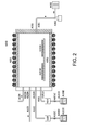
FIGURE 2 is a schematic illustration of a cross-section of a ALD reactor. -
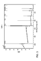
FIGURE 3 is an X-ray Photoelectron Spectroscopy (XPS) of a low etch SiO2 film. -
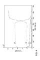
FIGURE 4 is a graph showing a depth profile of a bulk composition deposited in accordance with the present invention. - In one embodiment, this invention provides a method of forming silicon-based films that have extremely low wet etch rate in HF solution using a thermal CVD process. The said method comprises:
- a) Placing a substrate in a concealed reactor that is at a temperature of 400-700°C, is purged with Ar or N2 gas and maintained at a pressure below 1 Torr (130 Pa);
- b) Feeding the reactor with a silicon precursor that is delivered using a direct liquid injector and has one of the following structures:
R1 nR2 mSi(NR3R4)4-n-m;
and,
a cyclic silazane of (R1R2SiNR3)p; such as:
- c) At the same time, feeding the reactor with oxygen precursor such as pure oxygen or ozone;
- d) A pressure of 100 mTorr to 600 mTorr (13 to 80 Pa) is maintained during the deposition process.
- In another embodiment, this invention provides a method of forming silicon dioxide films that have extremely low wet etch rate in HF solution using an atomic layer deposition process. The said method comprises:
- a) Placing a substrate in a concealed reactor that is at a temperature of 100-600°C, is purged with Ar or N2 gas and maintained at a pressure below 1 Torr (130 Pa);
- b) Feeding the reactor with a silicon precursor that is delivered using a direct liquid injector and has one of the following structures:
R1 nR2 mSi(NR3R4)4-n-m;
and,
a cyclic silazane of (R1R2SiNR3)p; such as:
- c) The dose of the silicon precursor is just enough to form a monolayer of the precursor molecule on the surface of the substrate. The excess of the precursor is removed from the reactor;
- d) After the reactor is purged with Ar or N2 again, feeding the reactor with oxygen precursor such as pure oxygen or ozone; Again, the dose of the oxygen precursor is just enough to completely react with the monolayer silicon precursor on the substrate formed during the last step, and following this dose the reactor is again purged with Ar or N2;
- e) Repeating the steps b) to d) until a desired thick of the film is reached.
- In another embodiment, this invention provides a method of forming silicon dioxide films that have extremely low wet etch rate in HF solution using a cyclic chemical vapor deposition process. The said method comprises:
- a) Placing a substrate in a concealed reactor that is at a temperature of 400-700°C, is purged with Ar or N2 gas and maintained at a pressure below 1 Torr (130 Pa);
- b) Feeding the reactor with a silicon precursor that is delivered using a direct liquid injector and has one of the following structures:
R1 nR2 mSi(NR3R4)4-n-m;
and,
a cyclic silazane of (R1R2SiNR3)p; such as:
- c) The dose of the silicon precursor is adjusted (increased or reduced) to achieve a desired deposition rate of the film;
- d) Feeding the reactor with oxygen precursor such as pure oxygen or ozone; Again, the dose of the oxygen precursor is adjusted (increased or reduced) to achieve a desired deposition rate of the film;
- e) Purging the reactor with Ar or N2;
- f) Repeating steps b) to e) until a desired thickness of the film is reached.
- The silicon precursor is preferably an amino vinylsilane precursor such as, but not limited to, Bis(isopropylamino)vinylmethylsilane (BIPAVNS),
Bis(isopropylamino)divinylsilane (BIPADVS), Bis(isopropylamino)vinylsilane,
Bis(isopropylamino)allylmethylsilane, Bis(isopropylamino)diallylsilane,
Bis(isopropylamino)allylsilane, Bis(t-butylamino)vinylmethylsilane, Bis(t-butylamino)divinylsilane, Bis(t-butylamino)vinylsilane, Bis(t-butylamino)allylmethylsilane,
Bis(t-butylamino)diallylsilane, Bis(t-butylamino)allylsilane,
Bis(diethylamino)vinylmethylsilane, Bis(diethylamino)divinylsilane,
Bis(diethylamino)vinylsilane, Bis(diethylamino)allylmethylsilane,
Bis(diethylamino)diallylsilane, Bis(diethylamino)allylsilane,
Bis(dimethylamino)vinylmethylsilane, Bis(dimethylamino)divinylsilane,
Bis(dimethylamino)vinylsilane, Bis(dimethylamino)allylmethylsilane,
Bis(dimethylamino)diallylsilane, Bis(dimethylamino)allylsilane,
Bis(methylethylamino)vinylmethylsilane, Bis(methylethylamino)divinylsilane,
Bis(methylethylamino)vinylsilane, Bis(methylethylamino)allylmethylsilane,
Bis(methylethylamino)diallylsilane, Bis(methylethylamino)allylsilane,
Dipiperidinovinylmethylsilane, Dipiperidinodivinylsilane, Dipiperidinovinylsilane,
Dipiperidinoallylmethylsilane, Dipiperidinodiallylsilane, Dipiperidinoallylsilane,
Dipyrrolidinovinylmethylsilane, Dipyrrolidinodivinylsilane, Dipyrrolidinovinylsilane,
Dipyrrolidinoallylmethylsilane, Dipyrrolidinodiallylsilane, Dipyrrolidinoallylsilane,
Tris(isopropylamino)vinylsilane, Tris(isopropylamino)allylsilane, Tris(t-butylamino)vinylsilane, Tris(t-butylamino)allylsilane, Tris(diethylamino)vinylsilane,
Tris(diethylamino)allylsilane, Tris(dimethylamino)vinylsilane,
Tris(dimethylamino)allylsilane, Tris(methylethylamino)vinylsilane,
Tris(methylethylamino)allylsilane, Tripiperidinovinylsilane, Tripiperidinoallylsilane,
Tripyrrolidinovinylsilane, Tripyrrolidinoallylsilane, 1,3,5-trivinyl-1,3,5-trimethylcyclotrisilazane, 1,3,5-trivinylcyclotrisilazane, 1,1,3,3,5,5-hexavinylcyclotrisilazane, 1,3,5-triallyl-1,3,5-trimethylcyclotrisilazane, 1,3,5-triallylcyclotrisilazane, 1,1,3,3,5,5-hexaallylcyclotrisilazane, 1,3,5,7-tetravinyl-1,3,5,7-tetramethylcyclotetrasilazane, 1,3,5,7-tetravinylcyclotetrasilazane, 1,1,3,3,5,5,7,7-octavinylcyclotetrasilazane, 1,3,5,7-tetraallyl-1,3,5,7-tetramethylcyclotetrasilazane,
1,3,5,7-tetraallylcyclotetrasilazane, 1,1,3,3,5,5,7,7-octaallylcyclotetrasilazane. - The particular precursor used in tests is Bis(iso-propylamino)vinylmethylsilane (BIPAVMS). Another similar precursor is Bis(iso-propylamino)divinylsilane (BIPADVS).
- The method described in this invention can be demonstrated using a low pressure hot wall CVD reactor illustrated in
Figure 1 . TheCVD reactor 300 is heated by the surroundingheating element 201. All thewafers 203 are loaded on to awafer holder 202 that ensures they are placed along the axis of the CVD reactor so that they can be heated uniformly within each wafer. The number of the wafers in a single run can be as many as 25. - Before the film deposition process starts, the CVD tube is filled with inert gas (e.g. Ar or N2) through
inlet 103 and then pumped using a vacuum pump or process pump 302 to a vacuum level below 1 mT (0.13 Pa) and exhausted throughabatement 303. The CVD reactor is then filled with inert gas again and heated to a temperature at which the deposition is set to begin. Once the CVD reactor reaches the set temperature, thevalve 103A is closed andvalves throttle valve 301. - The reactive gas (e.g. O2) flows into the CVD reactor through
inlet 102 and the flow rate is controlled by a mass flow controller (MFC). The silicon precursor is in liquid form and filled in aliquid container 101 D. High pressure He gas is used to help push the liquid into avaporizer 101 B that heats the liquid and vaporizes the liquid. The flow the liquid precursor is controlled using a liquid flow controller (LFC). The flow rate of the precursor vapor can be controlled byLFC 101C and the heating temperature of thevaporizer 101 B: for a given setting of LFC, the higher the temperature of the vaporizer, the bigger the flow rate of the precursor vapor; for a given temperature setting of the vaporizer, the higher the flow rate of the LCF, the bigger the flow rate of the precursor vapor. Thevalve 101A opens or stops the flow of the precursor vapor to the CVD reactor. - The pressure of the CVD reactor can be in the range of about 0.01T to about 1T (1.3 to 130 Pa). The flow rate of the reactive gas (e.g. O2) can be in the range of 5 sccm to 200 sccm. The flow rate of the Si precursor vapor can be in the range of 5 sccm to 200 sccm. The deposition temperature is the same as the reactor wall temperature. It can be in the range of 500°C to 700°C.
- The deposition time is pre-set for the process to yield films with a desired thickness. The deposition rate is dependent of many processing parameters, including: the deposition temperature, the flow rate of O2, the flow rate of carrier gas (He), the liquid mass flow of the Si precursor, the temperature of the vaporizer, and the pressure of the reactor. The vaporizer temperature can be in the range of 20°C to 150°C. At the vaporizer temperature of 55°C, the rate of the deposition is about 0.5 nm/min.
- The rate of the deposition of the SiO2 can be in the range of 0.1 nm to 10 nm per minute. The rate can be controlled by varying the deposition temperature, the vaporizer temperature, the flow of the LFC, the flow rate of the reactive of O2 gas and the pressure at the CVD reactor.
- The method of forming uniform nitrogen free silicon dioxide films using an ALD process can be demonstrated using an ALD reactor illustrated in
Figure 2 . An ALD reactor A200 consists of a chamber wall A300 and substrate holder A202. Both of them can be heated separately at different temperatures. Wafers (or substrates) A203A are placed on A202 during the deposition process. - Before the film deposition process starts, the ALD reactor A200 is filled with inert gas (e.g. Ar or N2) through inlet A104 and valve A104A and them pumped using a vacuum pump or process pump A302 to a vacuum level below 1 mT (0.13 Pa) and exhausted to abatement A303. The ALD reactor A200 is then filled with inert gas again and the substrate holder A202 and the reactor wall are heated by heaters A201 to a temperature at which the deposition is set to begin.
- The Si precursor is delivered from a vapor draw A101 that is heated by an electric heater A101 E surrounding Si precursor container A101 D and maintained at a constant temperature during the deposition. The flow of the Si precursor is controlled through a high speed ALD valve A101A, mass flow controller A101 B and valve A101C.
- The temperature is between 20°C to 100°C. Helium can be introduced simultaneous with the Si precursor through line A103 and valve A103A. The oxygen precursor is delivered through a container A102D having heater A102E through a high speed ALD valve A102A controlling line A102 along with mass flow controller A102B and valve A102C.
- The sequence of the ALD process is as follows:
- Feed silicon precursor reactor A200 for 0.1-10 seconds by closing valve A301 and opening valve A101A for the same amount of time;
- Purge reactor A200 for 0.5-5 seconds by closing valve A101A and opening valve A301 and A104A for the same amount of time;
- Feed oxygen into reactor A200 for 0.1-10 seconds by closing valve A301 and opening valve A102A for the same amount of time;
- Purge reactor A200 for 0.5-5 seconds by closing valve A102a and opening valve A301 for the same amount of time;
- Repeat the above cycles for a number of times until a desired thickness of the film is achieved.
- The cyclic CVD process of forming uniform nitrogen free silicon dioxide films can also be illustrated in
Figure 2 . The same ALD reactor can be used for the cyclic CVD process. The major difference in the cyclic CVD process to deposit uniform nitrogen free films is that the dosages of the silicon precursor and oxygen precursor can be much bigger than the ones used for ALD, and thus the deposition rate can be much higher than ALD. The deposition temperature, however, is 400-700°C, much higher than that used for ALD process. - The sequence of the cyclic CVD process is as follows:
- Feed silicon precursor reactor A200 for 5-20 seconds by closing valve A301 and opening valve A101A for the same amount of time;
- Purge reactor A200 for 0.1-1 seconds by closing valve A101A and opening valves A301 and A104A for the same amount of time
- Feed oxygen to reactor A200 for 5-20 seconds by closing valve A301 and opening valve A102A for the same amount of time;
- Purge reactor A200 for 0.1-1 seconds by closing valve A102A and opening valves A301 and A104A for the same amount of time;
- Repeat the above cycles for a number of times until a desired thickness of the film is achieved.
- The characterization of thickness and optical properties such as refractive index of the oxide films is performed using a FilmTek 2000SE ellipsometer. Spectroscopic reflection data at normal incidence (angle of incidence = 0°) are used for the data fitting. The range of wavelength of the light used is between 200 nm to 900 nm. Since the extinction coefficient (k) for SiO2 is zero when the wavelength of the light is between 200 nm and 4000 nm and the dispersion of SiO2 is well known, the data are only fit on the high frequency dielectric constant. The thickness and refractive index of the oxide film can be obtained by fitting the reflection data from the film to a pre-set physical model (e.g., the Lorentz Osicllator model). The RMSE (root of mean square error) is used to determine the goodness of the fitting and the valve has to be less than 1 % for the results of the measurement to be considered reliable.
- The characterization of the chemical composition of the films is accomplished with X-ray Photoelectron Spectrometry (XPS). The X-ray Photoelectron Spectroscopy experiments are performed on a PHI 5000 VersaProbe Spectrometer equipped with Multiple Channels Plates (MCD) and a focused Al monochromatic X-ray source. The low resolution survey scan is performed at 117.4 eV Pass Energy, 1.000 eV/Step and a 50 msec/step dwell time. The high resolution multiplex scans are performed at 23.50 eV Pass Energy, 0.100 eV/Step and a 100 msec/step dwell time. The analysis area is 200 microns in diameter with a take-off angle of 45°. The data is collected using vendor supplied software. CasaXPS is used to work up the data using transmission function corrected Area Sensitivity Factors (ASF). All spectra are charge corrected to CHx=284.8 eV. The etch rate is calibrated against 203 nm SiO2/Si and is approximately 120 A/min.
- The etch test is carried out at 1 wt% HF (in deionized (DI) water) solution. The films (deposited on Si wafers) are placed in HF solution for 30 seconds, followed by rinsing in DI wafer and drying before being measured again for the loss of the material during the etch. Two thermal silicon oxide films with a known and consistent etch rate as references are loaded in the same cassette with the films to be characterized and etched at the same time. The films, along with reference thermal oxide films, are measured for their thickness at 9 different points across the film surface before and after etch using an ellipsometer and a method described above. The etch rate is then calculated as the thickness reduction divided by the time that the films are immersed into the HF solution.
- Dielectric constants, k, are calculated from a C-V curve measured with a MDC 802B-150 Mercury Probe. It consists of a probe stage that holds the sample and forms electrical contacts on the film to be measured, a Keithley 236 source meter and HP4284A LCR meter for C-V measurement. Si wafers that have relatively low electrical resistivity (sheet resistance less than 0.02 ohm-cm) are used to deposit the films for C-V measurement. Front contact mode is used to form electrical contacts to the film. Liquid metal (mercury) is pushed out through a thin tube from a reservoir to the surface of the wafer to form two electrically conductive contacts. The contact areas are calculated based on the diameter of the tube from which the mercury is pushed out. The dielectric constant is then calculated from the formula: k = the capacitance x the contact area / the thickness of the film.
- A typical XPS of the highly uniform nitrogen free films is shown in
Figure 3 and the composition of the different elements including nitrogen is also listed in Table 1. As can be seen from bothFigure 3 and Table 1, no significant nitrogen is detected in the films.Table 1. Chemical Composition of the Low Etch Rate Silicon Dioxide Film (in at%) Elements O Si C N Concentration 70.4 20.5 7.9 1.2 - The silicon dioxide films formed using the said invention are measured for their thickness using an ellisopmeter. The film was etched in a 1 wt% HF solution along with standard thermal silicon dioxide. The etch rate was then calculated from film thickness measurements and compared with that of thermal oxide. The result is listed in Table 2. As can be seen from Table 2, the wet etch rate of the low etch rate SiO2 (Present Invention) is much lower than even thermal oxide film.
Table 2. Wet etch rate of low etch rate SiO2 and standard thermal SiO2 (A/min) Material After 15 second etch After 1 minute etch After 2 minute etch Thermal SiO2 43.2 27.6 29.4 Low etch SiO2 (Present Invention) 1.2 1.2 1.2 - Using an ATV PE0612 brand low pressure chemical vapor deposition (LPCVD) reactor we loaded twenty five 100 mm Si wafers per deposition run. Upon closing the door to the reactor, we would start the automatic system sequencer to begin the process. The sequence would initially pump the chamber down to a base pressure of ~1 - 5 mtorr (0.13 to 0.67 Pa) for about 10 minutes. Then the process would introduce nitrogen purge gas (~40 to 50 sccm) and begin control the chamber pressure using a throttle valve to obtain the proper process pressure (125 to 500 mtorr (17 to 67 Pa)). The process would then ramp the chamber up to the desired process temperature (550°C or 600°C), this would take approximately 30 minutes. Upon reaching the process temperature, the wafer temperature was allowed to stabilize for 30 minutes, while still allowing the nitrogen purge gas to flow and maintaining process pressure. After the stabilization period was complete, the nitrogen purge gas flow was shut off and the precursor (Bis(isopropylamino)vinylmethylsilane) and the oxygen began to flow while still maintaining the process pressure and temperature. The precursor (Bis(isopropylamino)vinylmethylsilane) flow was ~ 14 to 19 sccm. The oxygen flow was 20 sccm or 40 sccm. After the deposition step was completed, the precursor (Bis(isopropylamino)vinylmethylsilane) and the oxygen were turn off and the nitrogen purge gas was allow to flow. The throttle valve was set to open to allow for purging of the chamber of the precursor (Bis(isopropylamino)vinylmethylsilane) and oxygen. At this point the system began to ramp the process chamber down to ~60°C for unloading of the wafers. The ramp normally takes about 60 minutes to cool down. Upon completion of the process, the system will automatically backfill the chamber with nitrogen and bring it up to atmospheric pressure, and the door to chamber can be opened for unloading the wafers.
- Using a Rudolph FOCUS Automatic Ellipsometer, 3 to 20 wafers per deposition were measured. A nine point measuring pattern was used for each wafer. The average film thickness measured varied from 350A° to 1000A°, depending upon the process used. That means that means that the deposition rate varied from 5.8A°/min. to 17A°/min. Wafer thickness uniformity varied from 2.0% to 6.9%. The average refractive index measured varied from 1.4375 to 1.4828.
-
Figure 4 shows a Dynamic Secondary Ion Mass Spectroscopy (SIMS) depth profile elemental analysis of a silicon oxide film , which indicates the excellent composition uniformity of the film for silicon, oxygen, and carbon, as well as very low content of nitrogen.
Claims (10)
- A method of forming a silicon dioxide film that has extremely low wet etch rate in HF solution, wherein the method is a low pressure, thermal chemical vapor deposition method, atomic layer deposition method or cyclic chemical vapor deposition method, and comprises:a. delivering a first precursor that provides a source for silicon to a low pressure, thermal chemical vapor deposition, an atomic layer deposition or a cyclic chemical vapor deposition reactor, wherein the first precursor is selected from the group consisting of: R1 nR2 mSi(NR3R4)4-n-m, and a cyclic silazane of the formula (R1R2SiNR3)p; where R1 is a C2-C10 alkenyl or aromatic group; R2 is H, a C1-C10, linear, branched, or cyclic alky, a C2-C10 linear, branched, or cyclic alkenyl, or an aromatic group; R3 and R4 are each selected from H, a C1-C10, linear, branched, or cyclic alkyl, a C2-C10 linear, branched, or cyclic alkenyl, and an aromatic group, or are joined such that NR3R4 is a cyclic amine; and n=1 to 3, m=0 to 2, and p=3 or 4; andb. delivering a second precursor that provides a source for oxygen to the reactor.
- A low pressure, thermal chemical vapor deposition method according to Claim 1 of forming a silicon dioxide film that has extremely low wet etch rate in HF solution, the method comprising:a. delivering a first precursor that provides a source for silicon to a low pressure, thermal chemical vapor deposition reactor, wherein the first precursor is selected from the group consisting of: R1 nR2 mSi(NR3R4)4-n-m, and a cyclic silazane of the formula (R1R2SiNR3)p; where R1 is a C2-C10 alkenyl or aromatic group; R2 is H, a C1-C10, linear, branched, or cyclic alkyl, a C2-C10 linear, branched, or cyclic alkenyl, or an aromatic group; R3 and R4 are each selected from H, a C1-C10, linear, branched, or cyclic alkyl, a C2-C10 linear, branched, or cyclic alkenyl, and an aromatic group, or are joined such that NR3R4 is a cyclic amine; and n=1 to 3, m=0 to 2, and p=3 or 4;b. delivering a second precursor that provides a source for oxygen to the reactor;c. reacting the first and second precursors at a temperature of 400°C to 700°C and under a pressure of 13 to 130 Pa (100mT to 1T).
- An atomic layer deposition method according to Claim 1 of forming a silicon dioxide film that has extremely low wet etch rate in HF solution, the method comprising:a. delivering a first precursor that provides a source for silicon to an atomic layer deposition reactor, wherein the first precursor is selected from the group consisting of: R1 nR2 mSi(NR3R4)4-n-m, and a cyclic silazane of the formula (R1R2SiNR3)p; where R1 is a C2-C10 alkenyl or an aromatic group; R2 is H, a C1-C10, linear, branched, or cyclic alkyl, a C2-C10 linear, branched, or cyclic alkenyl, or an aromatic group; R3 and R4 are each selected from H, a C1-C10, linear, branched, or cyclic alkyl, a C2-C10 linear, branched, or cyclic alkenyl, and an aromatic group, or are joined such that NR3R4 is a cyclic amine; and n=1 to 3, m=0 to 2, and p=3 or 4;b. purging the reactor with an inert gas;c. delivering a second precursor that provides a source for oxygen to the reactor;d. purging the reactor with an inert gas;e. repeating steps (a) to (d) until a desired thickness of the film is achieved.
- A cyclic chemical vapor deposition method according to Claim 1 of forming a silicon dioxide film that has extremely low wet etch rate in HF solution, the method comprising:a. delivering a first precursor that provides a source for silicon to a cyclic chemical vapor deposition reactor, wherein the first precursor is selected from the group consisting of: R1 nR2 mSi(NR3R4)4-n-m, and a cyclic silazane of the formula (R1R2SiNR3)p; where R1 is a C2-C10 alkenyl or an aromatic group; R2 is H, a C1-C10, linear, branched, or cyclic alkyl, a C2-C10 linear, branched, or cyclic alkenyl, or an aromatic group; R3 and R4 are each selected from H, a C1-C10, linear, branched, or cyclic alkyl, a C2-C10 linear, branched, or cyclic alkenyl, and an aromatic group, or are joined such that NR3R4 is a cyclic amine; and n=1 to 3, m=0 to 2, and p=3 or 4;b. purging the reactor with an inert gas for 0.1 to 1 seconds;c. delivering a second precursor that provides a source of oxygen to the reactor;d. purging the reactor with an inert gas for 0.1 to 1 seconds;e. repeating steps (a) to (d) until a desired thickness of the film is achieved.
- The method of Claim 3 or 4, wherein the inert gas is Ar or N2.
- The method of any preceding claim, wherein R1 is selected from the group consisting of vinyl, allyl, and phenyl.
- The method of any preceding claim, wherein R2 is selected from the group consisting of methyl, vinyl, H and allyl.
- The method of any preceding claim, wherein R3 and R4 are each selected from the group consisting of isopropyl, t-butyl, ethyl, methyl and H, or are joined such that NR3R4 is piperidino or pyrrolidino.
- The method of any preceding claim, wherein the first precursor is Bis(isopropylamino)vinylmethylsilane.
- The method of any preceding claim, wherein the second precursor is selected from the group consisting of oxygen, ozone and mixtures thereof.
Applications Claiming Priority (1)
| Application Number | Priority Date | Filing Date | Title |
|---|---|---|---|
| US12/964,266 US8460753B2 (en) | 2010-12-09 | 2010-12-09 | Methods for depositing silicon dioxide or silicon oxide films using aminovinylsilanes |
Publications (2)
| Publication Number | Publication Date |
|---|---|
| EP2463404A1 true EP2463404A1 (en) | 2012-06-13 |
| EP2463404B1 EP2463404B1 (en) | 2019-10-23 |
Family
ID=45440145
Family Applications (1)
| Application Number | Title | Priority Date | Filing Date |
|---|---|---|---|
| EP11192787.7A Not-in-force EP2463404B1 (en) | 2010-12-09 | 2011-12-09 | Method for forming sio2 film |
Country Status (6)
| Country | Link |
|---|---|
| US (1) | US8460753B2 (en) |
| EP (1) | EP2463404B1 (en) |
| JP (1) | JP5357240B2 (en) |
| KR (1) | KR101404576B1 (en) |
| CN (2) | CN102534548A (en) |
| TW (1) | TWI444499B (en) |
Cited By (5)
| Publication number | Priority date | Publication date | Assignee | Title |
|---|---|---|---|---|
| DE102012203212A1 (en) * | 2012-03-01 | 2013-09-05 | Osram Opto Semiconductors Gmbh | Coating system useful for producing layer on substrate using growth process, preferably for performing atomic layer deposition, comprises supply container, in which liquid starting material for layer is provided, and evaporator unit |
| EP2650399A3 (en) * | 2012-04-12 | 2013-10-30 | Air Products And Chemicals, Inc. | High temperature atomic layer deposition of silicon oxide thin films |
| KR20190143489A (en) * | 2017-05-24 | 2019-12-30 | 버슘머트리얼즈 유에스, 엘엘씨 | Cyclosilazane functionalized as precursor for high growth rate silicon-containing films |
| CN112777565A (en) * | 2019-11-05 | 2021-05-11 | 中国科学院大连化学物理研究所 | Semiconductor photocatalytic water splitting method capable of inhibiting reverse reaction |
| US12057310B2 (en) | 2018-05-22 | 2024-08-06 | Versum Materials Us, Llc | Functionalized cyclosilazanes as precursors for high growth rate silicon-containing films |
Families Citing this family (21)
| Publication number | Priority date | Publication date | Assignee | Title |
|---|---|---|---|---|
| US9448564B2 (en) | 2013-02-15 | 2016-09-20 | Reno Technologies, Inc. | Gas delivery system for outputting fast square waves of process gas during semiconductor processing |
| US9188989B1 (en) | 2011-08-20 | 2015-11-17 | Daniel T. Mudd | Flow node to deliver process gas using a remote pressure measurement device |
| US9958302B2 (en) | 2011-08-20 | 2018-05-01 | Reno Technologies, Inc. | Flow control system, method, and apparatus |
| WO2014040002A2 (en) | 2012-09-10 | 2014-03-13 | Mudd Daniel T | Pressure based mass flow controller |
| KR101993355B1 (en) | 2013-03-13 | 2019-09-30 | 삼성전자주식회사 | Method of fabricating a semiconductor device |
| KR102195139B1 (en) * | 2014-02-20 | 2020-12-24 | 삼성전자주식회사 | Methods of manufacturing semiconductor devices |
| US9875888B2 (en) | 2014-10-03 | 2018-01-23 | Applied Materials, Inc. | High temperature silicon oxide atomic layer deposition technology |
| CN107429391B (en) * | 2014-10-24 | 2021-06-25 | 弗萨姆材料美国有限责任公司 | Compositions and methods of depositing silicon-containing films using the same |
| US10421766B2 (en) * | 2015-02-13 | 2019-09-24 | Versum Materials Us, Llc | Bisaminoalkoxysilane compounds and methods for using same to deposit silicon-containing films |
| WO2017112732A1 (en) * | 2015-12-21 | 2017-06-29 | Versum Materials Us, Llc | Compositions and methods using same for deposition of silicon-containing film |
| WO2017147150A1 (en) * | 2016-02-26 | 2017-08-31 | Versum Materials Us, Llc | Compositions and methods using same for deposition of silicon-containing film |
| US10303189B2 (en) | 2016-06-30 | 2019-05-28 | Reno Technologies, Inc. | Flow control system, method, and apparatus |
| US10679880B2 (en) | 2016-09-27 | 2020-06-09 | Ichor Systems, Inc. | Method of achieving improved transient response in apparatus for controlling flow and system for accomplishing same |
| US11144075B2 (en) | 2016-06-30 | 2021-10-12 | Ichor Systems, Inc. | Flow control system, method, and apparatus |
| US10838437B2 (en) | 2018-02-22 | 2020-11-17 | Ichor Systems, Inc. | Apparatus for splitting flow of process gas and method of operating same |
| US10663337B2 (en) | 2016-12-30 | 2020-05-26 | Ichor Systems, Inc. | Apparatus for controlling flow and method of calibrating same |
| JP7329045B2 (en) * | 2018-10-04 | 2023-08-17 | バーサム マテリアルズ ユーエス,リミティド ライアビリティ カンパニー | Compositions for high temperature atomic layer deposition of high quality silicon oxide thin films |
| KR102731213B1 (en) | 2018-12-21 | 2024-11-15 | 레르 리키드 쏘시에떼 아노님 뿌르 레드 에렉스뿔라따시옹 데 프로세데 조르즈 클로드 | Precursor and method for depositing Si-containing films using ALD at temperatures exceeding 550°C |
| TWI797640B (en) | 2020-06-18 | 2023-04-01 | 法商液態空氣喬治斯克勞帝方法研究開發股份有限公司 | Silicon-based self-assembling monolayer compositions and surface preparation using the same |
| CN116113725B (en) * | 2020-07-24 | 2025-10-31 | 弗萨姆材料美国有限责任公司 | Composition for germanium seed layer and method of using the same |
| JP7583186B2 (en) | 2021-03-03 | 2024-11-13 | アイコール・システムズ・インク | Fluid flow control system with manifold assembly - Patents.com |
Citations (6)
| Publication number | Priority date | Publication date | Assignee | Title |
|---|---|---|---|---|
| EP1464726A2 (en) * | 2003-04-01 | 2004-10-06 | Air Products And Chemicals, Inc. | CVD method for forming a porous low dielectric constant SiOCH film |
| US20070275568A1 (en) * | 2003-11-28 | 2007-11-29 | Hidenori Miyoshi | Insulation Film Forming Method, Insulation Film Forming System, And Semiconductor Device Manufacturing Method |
| EP2116632A2 (en) * | 2008-05-05 | 2009-11-11 | Air Products and Chemicals, Inc. | Porogens, porogenated precursors and methods for using the same to provide porous organosilica glass films with low dielectric constants |
| US20100120262A1 (en) | 2008-11-12 | 2010-05-13 | Air Products And Chemicals, Inc. | Amino Vinylsilane Precursors for Stressed SiN Films |
| EP2228465A1 (en) * | 2009-03-13 | 2010-09-15 | Air Products and Chemicals, Inc. | Methods for making dielectric films comprising silicon |
| US20100291321A1 (en) | 2009-05-13 | 2010-11-18 | Air Products And Chemicals, Inc. | Dielectric Barrier Deposition Using Nitrogen Containing Precursor |
Family Cites Families (14)
| Publication number | Priority date | Publication date | Assignee | Title |
|---|---|---|---|---|
| GB1352951A (en) * | 1971-12-08 | 1974-05-15 | Shell Int Research | Electrostatic coating of glass-fibre material |
| US4863755A (en) * | 1987-10-16 | 1989-09-05 | The Regents Of The University Of California | Plasma enhanced chemical vapor deposition of thin films of silicon nitride from cyclic organosilicon nitrogen precursors |
| JP3093070B2 (en) * | 1993-01-26 | 2000-10-03 | 大阪瓦斯株式会社 | CVD thin film forming equipment |
| US5976991A (en) * | 1998-06-11 | 1999-11-02 | Air Products And Chemicals, Inc. | Deposition of silicon dioxide and silicon oxynitride using bis(tertiarybutylamino) silane |
| JP4722269B2 (en) * | 2000-08-29 | 2011-07-13 | Azエレクトロニックマテリアルズ株式会社 | Low dielectric constant porous siliceous film, semiconductor device and coating composition, and method for producing low dielectric constant porous siliceous film |
| US6391803B1 (en) * | 2001-06-20 | 2002-05-21 | Samsung Electronics Co., Ltd. | Method of forming silicon containing thin films by atomic layer deposition utilizing trisdimethylaminosilane |
| KR100505668B1 (en) * | 2002-07-08 | 2005-08-03 | 삼성전자주식회사 | Method for forming silicon dioxide layer by atomic layer deposition |
| US6838125B2 (en) * | 2002-07-10 | 2005-01-04 | Applied Materials, Inc. | Method of film deposition using activated precursor gases |
| JP2006261434A (en) | 2005-03-17 | 2006-09-28 | L'air Liquide Sa Pour L'etude & L'exploitation Des Procede S Georges Claude | Method for forming silicon oxide film |
| US7312129B2 (en) * | 2006-01-25 | 2007-12-25 | Freescale Semiconductor, Inc. | Method for producing two gates controlling the same channel |
| JP5177617B2 (en) * | 2006-12-25 | 2013-04-03 | 独立行政法人産業技術総合研究所 | Silicon oxide thin film forming equipment |
| US7500397B2 (en) * | 2007-02-15 | 2009-03-10 | Air Products And Chemicals, Inc. | Activated chemical process for enhancing material properties of dielectric films |
| US9337054B2 (en) | 2007-06-28 | 2016-05-10 | Entegris, Inc. | Precursors for silicon dioxide gap fill |
| US8242029B2 (en) * | 2009-11-23 | 2012-08-14 | Asm International N.V. | Method for forming a silicon dioxide/metal oxide-nanolaminate with a desired wet etch rate |
-
2010
- 2010-12-09 US US12/964,266 patent/US8460753B2/en not_active Expired - Fee Related
-
2011
- 2011-12-05 TW TW100144719A patent/TWI444499B/en not_active IP Right Cessation
- 2011-12-08 KR KR1020110131008A patent/KR101404576B1/en not_active Expired - Fee Related
- 2011-12-08 JP JP2011268617A patent/JP5357240B2/en not_active Expired - Fee Related
- 2011-12-09 CN CN2011104239643A patent/CN102534548A/en active Pending
- 2011-12-09 CN CN201510580613.1A patent/CN105239055A/en active Pending
- 2011-12-09 EP EP11192787.7A patent/EP2463404B1/en not_active Not-in-force
Patent Citations (6)
| Publication number | Priority date | Publication date | Assignee | Title |
|---|---|---|---|---|
| EP1464726A2 (en) * | 2003-04-01 | 2004-10-06 | Air Products And Chemicals, Inc. | CVD method for forming a porous low dielectric constant SiOCH film |
| US20070275568A1 (en) * | 2003-11-28 | 2007-11-29 | Hidenori Miyoshi | Insulation Film Forming Method, Insulation Film Forming System, And Semiconductor Device Manufacturing Method |
| EP2116632A2 (en) * | 2008-05-05 | 2009-11-11 | Air Products and Chemicals, Inc. | Porogens, porogenated precursors and methods for using the same to provide porous organosilica glass films with low dielectric constants |
| US20100120262A1 (en) | 2008-11-12 | 2010-05-13 | Air Products And Chemicals, Inc. | Amino Vinylsilane Precursors for Stressed SiN Films |
| EP2228465A1 (en) * | 2009-03-13 | 2010-09-15 | Air Products and Chemicals, Inc. | Methods for making dielectric films comprising silicon |
| US20100291321A1 (en) | 2009-05-13 | 2010-11-18 | Air Products And Chemicals, Inc. | Dielectric Barrier Deposition Using Nitrogen Containing Precursor |
Cited By (12)
| Publication number | Priority date | Publication date | Assignee | Title |
|---|---|---|---|---|
| DE102012203212A1 (en) * | 2012-03-01 | 2013-09-05 | Osram Opto Semiconductors Gmbh | Coating system useful for producing layer on substrate using growth process, preferably for performing atomic layer deposition, comprises supply container, in which liquid starting material for layer is provided, and evaporator unit |
| DE102012203212B4 (en) | 2012-03-01 | 2025-02-27 | Osram Oled Gmbh | COATING SYSTEM AND METHOD FOR CARRYING OUT A GROWTH PROCESS |
| EP2650399A3 (en) * | 2012-04-12 | 2013-10-30 | Air Products And Chemicals, Inc. | High temperature atomic layer deposition of silicon oxide thin films |
| US9460912B2 (en) | 2012-04-12 | 2016-10-04 | Air Products And Chemicals, Inc. | High temperature atomic layer deposition of silicon oxide thin films |
| US10242864B2 (en) | 2012-04-12 | 2019-03-26 | Versum Materials Us, Llc | High temperature atomic layer deposition of silicon oxide thin films |
| KR20190143489A (en) * | 2017-05-24 | 2019-12-30 | 버슘머트리얼즈 유에스, 엘엘씨 | Cyclosilazane functionalized as precursor for high growth rate silicon-containing films |
| EP3630785A4 (en) * | 2017-05-24 | 2021-01-20 | Versum Materials US, LLC | FUNCTIONALIZED CYCLOSILAZANES USED AS PRECURSORS FOR FILMS CONTAINING SILICON AT HIGH GROWTH RATE |
| US11177127B2 (en) | 2017-05-24 | 2021-11-16 | Versum Materials Us, Llc | Functionalized cyclosilazanes as precursors for high growth rate silicon-containing films |
| EP4624625A3 (en) * | 2017-05-24 | 2025-12-31 | Versum Materials US, LLC | Functionalized cyclosilazanes as precursors for high-growth silicon-containing films |
| US12057310B2 (en) | 2018-05-22 | 2024-08-06 | Versum Materials Us, Llc | Functionalized cyclosilazanes as precursors for high growth rate silicon-containing films |
| CN112777565A (en) * | 2019-11-05 | 2021-05-11 | 中国科学院大连化学物理研究所 | Semiconductor photocatalytic water splitting method capable of inhibiting reverse reaction |
| CN112777565B (en) * | 2019-11-05 | 2022-11-22 | 中国科学院大连化学物理研究所 | Semiconductor photocatalytic water splitting method capable of inhibiting reverse reaction |
Also Published As
| Publication number | Publication date |
|---|---|
| US20120148745A1 (en) | 2012-06-14 |
| KR20120064635A (en) | 2012-06-19 |
| KR101404576B1 (en) | 2014-06-09 |
| US8460753B2 (en) | 2013-06-11 |
| CN105239055A (en) | 2016-01-13 |
| JP2012124492A (en) | 2012-06-28 |
| TWI444499B (en) | 2014-07-11 |
| CN102534548A (en) | 2012-07-04 |
| JP5357240B2 (en) | 2013-12-04 |
| TW201224193A (en) | 2012-06-16 |
| EP2463404B1 (en) | 2019-10-23 |
Similar Documents
| Publication | Publication Date | Title |
|---|---|---|
| EP2463404B1 (en) | Method for forming sio2 film | |
| US6217658B1 (en) | Sequencing of the recipe steps for the optimal low-dielectric constant HDP-CVD Processing | |
| US6660662B2 (en) | Method of reducing plasma charge damage for plasma processes | |
| JP5252417B2 (en) | Process sequence of deep trench doped silicon filling | |
| EP0874391B1 (en) | Process for depositing a Halogen-doped SiO2 layer | |
| US20110151142A1 (en) | Pecvd multi-step processing with continuous plasma | |
| US20020094388A1 (en) | Low temperature, high quality silicon dioxide thin films deposited using tetramethylsilane (TMS) for stress control and coverage applications | |
| KR20180116761A (en) | Method of Plasma-Assisted Cyclic Deposition Using Ramp-Down Flow of Reactant Gas | |
| EP2228465B1 (en) | Methods for making dielectric films comprising silicon | |
| WO2007044145A2 (en) | Method and apparatus for the low temperature deposition of doped silicon nitride films | |
| Li et al. | Effect of process pressure on atomic layer deposition of Al2O3 | |
| US20230143678A1 (en) | Method and system for depositing boron nitride using pulsed chemical vapor deposition | |
| JP2003224126A (en) | Systems and methods for improved thin dielectric films | |
| US10593543B2 (en) | Method of depositing doped amorphous silicon films with enhanced defect control, reduced substrate sensitivity to in-film defects and bubble-free film growth | |
| Wang et al. | Study of oxygen influences on carbon doped silicon oxide low k thin films deposited by plasma enhanced chemical vapor deposition | |
| EP0187826B1 (en) | Fabrication of devices with a silicon oxide region | |
| KR101008490B1 (en) | Oxide film deposition method by low temperature chemical vapor deposition | |
| Katz et al. | Fast thermal kinetic growth of silicon dioxide films on InP by rapid thermal low-pressure chemical vapour deposition | |
| van Hemmen et al. | Remote plasma and thermal ALD of Al2O3 for trench capacitor applications | |
| Chen | Synthesis and characterization of silicon dioxide thin films by plasma enhances chemical vapor deposition from diethylsilane and nitrous oxide |
Legal Events
| Date | Code | Title | Description |
|---|---|---|---|
| PUAI | Public reference made under article 153(3) epc to a published international application that has entered the european phase |
Free format text: ORIGINAL CODE: 0009012 |
|
| AK | Designated contracting states |
Kind code of ref document: A1 Designated state(s): AL AT BE BG CH CY CZ DE DK EE ES FI FR GB GR HR HU IE IS IT LI LT LU LV MC MK MT NL NO PL PT RO RS SE SI SK SM TR |
|
| AX | Request for extension of the european patent |
Extension state: BA ME |
|
| 17P | Request for examination filed |
Effective date: 20121213 |
|
| STAA | Information on the status of an ep patent application or granted ep patent |
Free format text: STATUS: EXAMINATION IS IN PROGRESS |
|
| 17Q | First examination report despatched |
Effective date: 20170718 |
|
| RAP1 | Party data changed (applicant data changed or rights of an application transferred) |
Owner name: VERSUM MATERIALS US, LLC |
|
| GRAJ | Information related to disapproval of communication of intention to grant by the applicant or resumption of examination proceedings by the epo deleted |
Free format text: ORIGINAL CODE: EPIDOSDIGR1 |
|
| GRAP | Despatch of communication of intention to grant a patent |
Free format text: ORIGINAL CODE: EPIDOSNIGR1 |
|
| STAA | Information on the status of an ep patent application or granted ep patent |
Free format text: STATUS: EXAMINATION IS IN PROGRESS |
|
| GRAJ | Information related to disapproval of communication of intention to grant by the applicant or resumption of examination proceedings by the epo deleted |
Free format text: ORIGINAL CODE: EPIDOSDIGR1 |
|
| INTG | Intention to grant announced |
Effective date: 20190423 |
|
| INTC | Intention to grant announced (deleted) | ||
| GRAP | Despatch of communication of intention to grant a patent |
Free format text: ORIGINAL CODE: EPIDOSNIGR1 |
|
| STAA | Information on the status of an ep patent application or granted ep patent |
Free format text: STATUS: GRANT OF PATENT IS INTENDED |
|
| INTG | Intention to grant announced |
Effective date: 20190712 |
|
| GRAS | Grant fee paid |
Free format text: ORIGINAL CODE: EPIDOSNIGR3 |
|
| GRAA | (expected) grant |
Free format text: ORIGINAL CODE: 0009210 |
|
| STAA | Information on the status of an ep patent application or granted ep patent |
Free format text: STATUS: THE PATENT HAS BEEN GRANTED |
|
| AK | Designated contracting states |
Kind code of ref document: B1 Designated state(s): AL AT BE BG CH CY CZ DE DK EE ES FI FR GB GR HR HU IE IS IT LI LT LU LV MC MK MT NL NO PL PT RO RS SE SI SK SM TR |
|
| REG | Reference to a national code |
Ref country code: GB Ref legal event code: FG4D |
|
| REG | Reference to a national code |
Ref country code: CH Ref legal event code: EP |
|
| REG | Reference to a national code |
Ref country code: IE Ref legal event code: FG4D |
|
| REG | Reference to a national code |
Ref country code: DE Ref legal event code: R096 Ref document number: 602011062871 Country of ref document: DE |
|
| REG | Reference to a national code |
Ref country code: AT Ref legal event code: REF Ref document number: 1193702 Country of ref document: AT Kind code of ref document: T Effective date: 20191115 |
|
| REG | Reference to a national code |
Ref country code: NL Ref legal event code: MP Effective date: 20191023 |
|
| REG | Reference to a national code |
Ref country code: LT Ref legal event code: MG4D |
|
| PG25 | Lapsed in a contracting state [announced via postgrant information from national office to epo] |
Ref country code: PT Free format text: LAPSE BECAUSE OF FAILURE TO SUBMIT A TRANSLATION OF THE DESCRIPTION OR TO PAY THE FEE WITHIN THE PRESCRIBED TIME-LIMIT Effective date: 20200224 Ref country code: NL Free format text: LAPSE BECAUSE OF FAILURE TO SUBMIT A TRANSLATION OF THE DESCRIPTION OR TO PAY THE FEE WITHIN THE PRESCRIBED TIME-LIMIT Effective date: 20191023 Ref country code: PL Free format text: LAPSE BECAUSE OF FAILURE TO SUBMIT A TRANSLATION OF THE DESCRIPTION OR TO PAY THE FEE WITHIN THE PRESCRIBED TIME-LIMIT Effective date: 20191023 Ref country code: BG Free format text: LAPSE BECAUSE OF FAILURE TO SUBMIT A TRANSLATION OF THE DESCRIPTION OR TO PAY THE FEE WITHIN THE PRESCRIBED TIME-LIMIT Effective date: 20200123 Ref country code: LT Free format text: LAPSE BECAUSE OF FAILURE TO SUBMIT A TRANSLATION OF THE DESCRIPTION OR TO PAY THE FEE WITHIN THE PRESCRIBED TIME-LIMIT Effective date: 20191023 Ref country code: ES Free format text: LAPSE BECAUSE OF FAILURE TO SUBMIT A TRANSLATION OF THE DESCRIPTION OR TO PAY THE FEE WITHIN THE PRESCRIBED TIME-LIMIT Effective date: 20191023 Ref country code: FI Free format text: LAPSE BECAUSE OF FAILURE TO SUBMIT A TRANSLATION OF THE DESCRIPTION OR TO PAY THE FEE WITHIN THE PRESCRIBED TIME-LIMIT Effective date: 20191023 Ref country code: GR Free format text: LAPSE BECAUSE OF FAILURE TO SUBMIT A TRANSLATION OF THE DESCRIPTION OR TO PAY THE FEE WITHIN THE PRESCRIBED TIME-LIMIT Effective date: 20200124 Ref country code: LV Free format text: LAPSE BECAUSE OF FAILURE TO SUBMIT A TRANSLATION OF THE DESCRIPTION OR TO PAY THE FEE WITHIN THE PRESCRIBED TIME-LIMIT Effective date: 20191023 Ref country code: SE Free format text: LAPSE BECAUSE OF FAILURE TO SUBMIT A TRANSLATION OF THE DESCRIPTION OR TO PAY THE FEE WITHIN THE PRESCRIBED TIME-LIMIT Effective date: 20191023 Ref country code: NO Free format text: LAPSE BECAUSE OF FAILURE TO SUBMIT A TRANSLATION OF THE DESCRIPTION OR TO PAY THE FEE WITHIN THE PRESCRIBED TIME-LIMIT Effective date: 20200123 |
|
| PG25 | Lapsed in a contracting state [announced via postgrant information from national office to epo] |
Ref country code: IS Free format text: LAPSE BECAUSE OF FAILURE TO SUBMIT A TRANSLATION OF THE DESCRIPTION OR TO PAY THE FEE WITHIN THE PRESCRIBED TIME-LIMIT Effective date: 20200224 Ref country code: RS Free format text: LAPSE BECAUSE OF FAILURE TO SUBMIT A TRANSLATION OF THE DESCRIPTION OR TO PAY THE FEE WITHIN THE PRESCRIBED TIME-LIMIT Effective date: 20191023 Ref country code: HR Free format text: LAPSE BECAUSE OF FAILURE TO SUBMIT A TRANSLATION OF THE DESCRIPTION OR TO PAY THE FEE WITHIN THE PRESCRIBED TIME-LIMIT Effective date: 20191023 |
|
| PG25 | Lapsed in a contracting state [announced via postgrant information from national office to epo] |
Ref country code: AL Free format text: LAPSE BECAUSE OF FAILURE TO SUBMIT A TRANSLATION OF THE DESCRIPTION OR TO PAY THE FEE WITHIN THE PRESCRIBED TIME-LIMIT Effective date: 20191023 |
|
| REG | Reference to a national code |
Ref country code: DE Ref legal event code: R097 Ref document number: 602011062871 Country of ref document: DE |
|
| PG2D | Information on lapse in contracting state deleted |
Ref country code: IS |
|
| PG25 | Lapsed in a contracting state [announced via postgrant information from national office to epo] |
Ref country code: EE Free format text: LAPSE BECAUSE OF FAILURE TO SUBMIT A TRANSLATION OF THE DESCRIPTION OR TO PAY THE FEE WITHIN THE PRESCRIBED TIME-LIMIT Effective date: 20191023 Ref country code: CZ Free format text: LAPSE BECAUSE OF FAILURE TO SUBMIT A TRANSLATION OF THE DESCRIPTION OR TO PAY THE FEE WITHIN THE PRESCRIBED TIME-LIMIT Effective date: 20191023 Ref country code: RO Free format text: LAPSE BECAUSE OF FAILURE TO SUBMIT A TRANSLATION OF THE DESCRIPTION OR TO PAY THE FEE WITHIN THE PRESCRIBED TIME-LIMIT Effective date: 20191023 Ref country code: DK Free format text: LAPSE BECAUSE OF FAILURE TO SUBMIT A TRANSLATION OF THE DESCRIPTION OR TO PAY THE FEE WITHIN THE PRESCRIBED TIME-LIMIT Effective date: 20191023 Ref country code: IS Free format text: LAPSE BECAUSE OF FAILURE TO SUBMIT A TRANSLATION OF THE DESCRIPTION OR TO PAY THE FEE WITHIN THE PRESCRIBED TIME-LIMIT Effective date: 20200223 |
|
| REG | Reference to a national code |
Ref country code: CH Ref legal event code: PL |
|
| REG | Reference to a national code |
Ref country code: AT Ref legal event code: MK05 Ref document number: 1193702 Country of ref document: AT Kind code of ref document: T Effective date: 20191023 |
|
| REG | Reference to a national code |
Ref country code: BE Ref legal event code: MM Effective date: 20191231 |
|
| PLBE | No opposition filed within time limit |
Free format text: ORIGINAL CODE: 0009261 |
|
| STAA | Information on the status of an ep patent application or granted ep patent |
Free format text: STATUS: NO OPPOSITION FILED WITHIN TIME LIMIT |
|
| PG25 | Lapsed in a contracting state [announced via postgrant information from national office to epo] |
Ref country code: MC Free format text: LAPSE BECAUSE OF FAILURE TO SUBMIT A TRANSLATION OF THE DESCRIPTION OR TO PAY THE FEE WITHIN THE PRESCRIBED TIME-LIMIT Effective date: 20191023 Ref country code: SK Free format text: LAPSE BECAUSE OF FAILURE TO SUBMIT A TRANSLATION OF THE DESCRIPTION OR TO PAY THE FEE WITHIN THE PRESCRIBED TIME-LIMIT Effective date: 20191023 Ref country code: SM Free format text: LAPSE BECAUSE OF FAILURE TO SUBMIT A TRANSLATION OF THE DESCRIPTION OR TO PAY THE FEE WITHIN THE PRESCRIBED TIME-LIMIT Effective date: 20191023 Ref country code: IT Free format text: LAPSE BECAUSE OF FAILURE TO SUBMIT A TRANSLATION OF THE DESCRIPTION OR TO PAY THE FEE WITHIN THE PRESCRIBED TIME-LIMIT Effective date: 20191023 |
|
| GBPC | Gb: european patent ceased through non-payment of renewal fee |
Effective date: 20200123 |
|
| 26N | No opposition filed |
Effective date: 20200724 |
|
| PG25 | Lapsed in a contracting state [announced via postgrant information from national office to epo] |
Ref country code: GB Free format text: LAPSE BECAUSE OF NON-PAYMENT OF DUE FEES Effective date: 20200123 Ref country code: LU Free format text: LAPSE BECAUSE OF NON-PAYMENT OF DUE FEES Effective date: 20191209 |
|
| PG25 | Lapsed in a contracting state [announced via postgrant information from national office to epo] |
Ref country code: SI Free format text: LAPSE BECAUSE OF FAILURE TO SUBMIT A TRANSLATION OF THE DESCRIPTION OR TO PAY THE FEE WITHIN THE PRESCRIBED TIME-LIMIT Effective date: 20191023 Ref country code: LI Free format text: LAPSE BECAUSE OF NON-PAYMENT OF DUE FEES Effective date: 20191231 Ref country code: BE Free format text: LAPSE BECAUSE OF NON-PAYMENT OF DUE FEES Effective date: 20191231 Ref country code: AT Free format text: LAPSE BECAUSE OF FAILURE TO SUBMIT A TRANSLATION OF THE DESCRIPTION OR TO PAY THE FEE WITHIN THE PRESCRIBED TIME-LIMIT Effective date: 20191023 Ref country code: CH Free format text: LAPSE BECAUSE OF NON-PAYMENT OF DUE FEES Effective date: 20191231 |
|
| PG25 | Lapsed in a contracting state [announced via postgrant information from national office to epo] |
Ref country code: CY Free format text: LAPSE BECAUSE OF FAILURE TO SUBMIT A TRANSLATION OF THE DESCRIPTION OR TO PAY THE FEE WITHIN THE PRESCRIBED TIME-LIMIT Effective date: 20191023 |
|
| PG25 | Lapsed in a contracting state [announced via postgrant information from national office to epo] |
Ref country code: HU Free format text: LAPSE BECAUSE OF FAILURE TO SUBMIT A TRANSLATION OF THE DESCRIPTION OR TO PAY THE FEE WITHIN THE PRESCRIBED TIME-LIMIT; INVALID AB INITIO Effective date: 20111209 Ref country code: MT Free format text: LAPSE BECAUSE OF FAILURE TO SUBMIT A TRANSLATION OF THE DESCRIPTION OR TO PAY THE FEE WITHIN THE PRESCRIBED TIME-LIMIT Effective date: 20191023 |
|
| PGFP | Annual fee paid to national office [announced via postgrant information from national office to epo] |
Ref country code: DE Payment date: 20211012 Year of fee payment: 11 Ref country code: FR Payment date: 20211109 Year of fee payment: 11 Ref country code: IE Payment date: 20211109 Year of fee payment: 11 |
|
| PG25 | Lapsed in a contracting state [announced via postgrant information from national office to epo] |
Ref country code: TR Free format text: LAPSE BECAUSE OF FAILURE TO SUBMIT A TRANSLATION OF THE DESCRIPTION OR TO PAY THE FEE WITHIN THE PRESCRIBED TIME-LIMIT Effective date: 20191023 |
|
| PG25 | Lapsed in a contracting state [announced via postgrant information from national office to epo] |
Ref country code: MK Free format text: LAPSE BECAUSE OF FAILURE TO SUBMIT A TRANSLATION OF THE DESCRIPTION OR TO PAY THE FEE WITHIN THE PRESCRIBED TIME-LIMIT Effective date: 20191023 |
|
| REG | Reference to a national code |
Ref country code: DE Ref legal event code: R119 Ref document number: 602011062871 Country of ref document: DE |
|
| P01 | Opt-out of the competence of the unified patent court (upc) registered |
Effective date: 20230602 |
|
| PG25 | Lapsed in a contracting state [announced via postgrant information from national office to epo] |
Ref country code: IE Free format text: LAPSE BECAUSE OF NON-PAYMENT OF DUE FEES Effective date: 20221209 Ref country code: DE Free format text: LAPSE BECAUSE OF NON-PAYMENT OF DUE FEES Effective date: 20230701 |
|
| PG25 | Lapsed in a contracting state [announced via postgrant information from national office to epo] |
Ref country code: FR Free format text: LAPSE BECAUSE OF NON-PAYMENT OF DUE FEES Effective date: 20221231 |