EP2462788B1 - Assembly and method for illuminating through a circuit board - Google Patents
Assembly and method for illuminating through a circuit board Download PDFInfo
- Publication number
- EP2462788B1 EP2462788B1 EP09848136.9A EP09848136A EP2462788B1 EP 2462788 B1 EP2462788 B1 EP 2462788B1 EP 09848136 A EP09848136 A EP 09848136A EP 2462788 B1 EP2462788 B1 EP 2462788B1
- Authority
- EP
- European Patent Office
- Prior art keywords
- flexible layer
- adhesive
- substrate
- light
- assembly according
- Prior art date
- Legal status (The legal status is an assumption and is not a legal conclusion. Google has not performed a legal analysis and makes no representation as to the accuracy of the status listed.)
- Not-in-force
Links
Images







Classifications
-
- B—PERFORMING OPERATIONS; TRANSPORTING
- B32—LAYERED PRODUCTS
- B32B—LAYERED PRODUCTS, i.e. PRODUCTS BUILT-UP OF STRATA OF FLAT OR NON-FLAT, e.g. CELLULAR OR HONEYCOMB, FORM
- B32B7/00—Layered products characterised by the relation between layers; Layered products characterised by the relative orientation of features between layers, or by the relative values of a measurable parameter between layers, i.e. products comprising layers having different physical, chemical or physicochemical properties; Layered products characterised by the interconnection of layers
- B32B7/04—Interconnection of layers
- B32B7/12—Interconnection of layers using interposed adhesives or interposed materials with bonding properties
-
- B—PERFORMING OPERATIONS; TRANSPORTING
- B32—LAYERED PRODUCTS
- B32B—LAYERED PRODUCTS, i.e. PRODUCTS BUILT-UP OF STRATA OF FLAT OR NON-FLAT, e.g. CELLULAR OR HONEYCOMB, FORM
- B32B27/00—Layered products comprising a layer of synthetic resin
- B32B27/06—Layered products comprising a layer of synthetic resin as the main or only constituent of a layer, which is next to another layer of the same or of a different material
- B32B27/08—Layered products comprising a layer of synthetic resin as the main or only constituent of a layer, which is next to another layer of the same or of a different material of synthetic resin
-
- B—PERFORMING OPERATIONS; TRANSPORTING
- B32—LAYERED PRODUCTS
- B32B—LAYERED PRODUCTS, i.e. PRODUCTS BUILT-UP OF STRATA OF FLAT OR NON-FLAT, e.g. CELLULAR OR HONEYCOMB, FORM
- B32B27/00—Layered products comprising a layer of synthetic resin
- B32B27/28—Layered products comprising a layer of synthetic resin comprising synthetic resins not wholly covered by any one of the sub-groups B32B27/30 - B32B27/42
- B32B27/283—Layered products comprising a layer of synthetic resin comprising synthetic resins not wholly covered by any one of the sub-groups B32B27/30 - B32B27/42 comprising polysiloxanes
-
- B—PERFORMING OPERATIONS; TRANSPORTING
- B32—LAYERED PRODUCTS
- B32B—LAYERED PRODUCTS, i.e. PRODUCTS BUILT-UP OF STRATA OF FLAT OR NON-FLAT, e.g. CELLULAR OR HONEYCOMB, FORM
- B32B27/00—Layered products comprising a layer of synthetic resin
- B32B27/30—Layered products comprising a layer of synthetic resin comprising vinyl (co)polymers; comprising acrylic (co)polymers
- B32B27/302—Layered products comprising a layer of synthetic resin comprising vinyl (co)polymers; comprising acrylic (co)polymers comprising aromatic vinyl (co)polymers, e.g. styrenic (co)polymers
-
- B—PERFORMING OPERATIONS; TRANSPORTING
- B32—LAYERED PRODUCTS
- B32B—LAYERED PRODUCTS, i.e. PRODUCTS BUILT-UP OF STRATA OF FLAT OR NON-FLAT, e.g. CELLULAR OR HONEYCOMB, FORM
- B32B27/00—Layered products comprising a layer of synthetic resin
- B32B27/30—Layered products comprising a layer of synthetic resin comprising vinyl (co)polymers; comprising acrylic (co)polymers
- B32B27/304—Layered products comprising a layer of synthetic resin comprising vinyl (co)polymers; comprising acrylic (co)polymers comprising vinyl halide (co)polymers, e.g. PVC, PVDC, PVF, PVDF
-
- B—PERFORMING OPERATIONS; TRANSPORTING
- B32—LAYERED PRODUCTS
- B32B—LAYERED PRODUCTS, i.e. PRODUCTS BUILT-UP OF STRATA OF FLAT OR NON-FLAT, e.g. CELLULAR OR HONEYCOMB, FORM
- B32B27/00—Layered products comprising a layer of synthetic resin
- B32B27/30—Layered products comprising a layer of synthetic resin comprising vinyl (co)polymers; comprising acrylic (co)polymers
- B32B27/308—Layered products comprising a layer of synthetic resin comprising vinyl (co)polymers; comprising acrylic (co)polymers comprising acrylic (co)polymers
-
- B—PERFORMING OPERATIONS; TRANSPORTING
- B32—LAYERED PRODUCTS
- B32B—LAYERED PRODUCTS, i.e. PRODUCTS BUILT-UP OF STRATA OF FLAT OR NON-FLAT, e.g. CELLULAR OR HONEYCOMB, FORM
- B32B27/00—Layered products comprising a layer of synthetic resin
- B32B27/32—Layered products comprising a layer of synthetic resin comprising polyolefins
-
- B—PERFORMING OPERATIONS; TRANSPORTING
- B32—LAYERED PRODUCTS
- B32B—LAYERED PRODUCTS, i.e. PRODUCTS BUILT-UP OF STRATA OF FLAT OR NON-FLAT, e.g. CELLULAR OR HONEYCOMB, FORM
- B32B27/00—Layered products comprising a layer of synthetic resin
- B32B27/32—Layered products comprising a layer of synthetic resin comprising polyolefins
- B32B27/322—Layered products comprising a layer of synthetic resin comprising polyolefins comprising halogenated polyolefins, e.g. PTFE
-
- B—PERFORMING OPERATIONS; TRANSPORTING
- B32—LAYERED PRODUCTS
- B32B—LAYERED PRODUCTS, i.e. PRODUCTS BUILT-UP OF STRATA OF FLAT OR NON-FLAT, e.g. CELLULAR OR HONEYCOMB, FORM
- B32B27/00—Layered products comprising a layer of synthetic resin
- B32B27/36—Layered products comprising a layer of synthetic resin comprising polyesters
- B32B27/365—Layered products comprising a layer of synthetic resin comprising polyesters comprising polycarbonates
-
- B—PERFORMING OPERATIONS; TRANSPORTING
- B32—LAYERED PRODUCTS
- B32B—LAYERED PRODUCTS, i.e. PRODUCTS BUILT-UP OF STRATA OF FLAT OR NON-FLAT, e.g. CELLULAR OR HONEYCOMB, FORM
- B32B2250/00—Layers arrangement
- B32B2250/24—All layers being polymeric
-
- B—PERFORMING OPERATIONS; TRANSPORTING
- B32—LAYERED PRODUCTS
- B32B—LAYERED PRODUCTS, i.e. PRODUCTS BUILT-UP OF STRATA OF FLAT OR NON-FLAT, e.g. CELLULAR OR HONEYCOMB, FORM
- B32B2307/00—Properties of the layers or laminate
- B32B2307/20—Properties of the layers or laminate having particular electrical or magnetic properties, e.g. piezoelectric
- B32B2307/204—Di-electric
-
- B—PERFORMING OPERATIONS; TRANSPORTING
- B32—LAYERED PRODUCTS
- B32B—LAYERED PRODUCTS, i.e. PRODUCTS BUILT-UP OF STRATA OF FLAT OR NON-FLAT, e.g. CELLULAR OR HONEYCOMB, FORM
- B32B2307/00—Properties of the layers or laminate
- B32B2307/40—Properties of the layers or laminate having particular optical properties
- B32B2307/402—Coloured
-
- B—PERFORMING OPERATIONS; TRANSPORTING
- B32—LAYERED PRODUCTS
- B32B—LAYERED PRODUCTS, i.e. PRODUCTS BUILT-UP OF STRATA OF FLAT OR NON-FLAT, e.g. CELLULAR OR HONEYCOMB, FORM
- B32B2307/00—Properties of the layers or laminate
- B32B2307/40—Properties of the layers or laminate having particular optical properties
- B32B2307/412—Transparent
-
- B—PERFORMING OPERATIONS; TRANSPORTING
- B32—LAYERED PRODUCTS
- B32B—LAYERED PRODUCTS, i.e. PRODUCTS BUILT-UP OF STRATA OF FLAT OR NON-FLAT, e.g. CELLULAR OR HONEYCOMB, FORM
- B32B2307/00—Properties of the layers or laminate
- B32B2307/40—Properties of the layers or laminate having particular optical properties
- B32B2307/414—Translucent
-
- B—PERFORMING OPERATIONS; TRANSPORTING
- B32—LAYERED PRODUCTS
- B32B—LAYERED PRODUCTS, i.e. PRODUCTS BUILT-UP OF STRATA OF FLAT OR NON-FLAT, e.g. CELLULAR OR HONEYCOMB, FORM
- B32B2307/00—Properties of the layers or laminate
- B32B2307/50—Properties of the layers or laminate having particular mechanical properties
- B32B2307/546—Flexural strength; Flexion stiffness
-
- B—PERFORMING OPERATIONS; TRANSPORTING
- B32—LAYERED PRODUCTS
- B32B—LAYERED PRODUCTS, i.e. PRODUCTS BUILT-UP OF STRATA OF FLAT OR NON-FLAT, e.g. CELLULAR OR HONEYCOMB, FORM
- B32B2457/00—Electrical equipment
- B32B2457/08—PCBs, i.e. printed circuit boards
-
- Y—GENERAL TAGGING OF NEW TECHNOLOGICAL DEVELOPMENTS; GENERAL TAGGING OF CROSS-SECTIONAL TECHNOLOGIES SPANNING OVER SEVERAL SECTIONS OF THE IPC; TECHNICAL SUBJECTS COVERED BY FORMER USPC CROSS-REFERENCE ART COLLECTIONS [XRACs] AND DIGESTS
- Y10—TECHNICAL SUBJECTS COVERED BY FORMER USPC
- Y10T—TECHNICAL SUBJECTS COVERED BY FORMER US CLASSIFICATION
- Y10T156/00—Adhesive bonding and miscellaneous chemical manufacture
- Y10T156/10—Methods of surface bonding and/or assembly therefor
-
- Y—GENERAL TAGGING OF NEW TECHNOLOGICAL DEVELOPMENTS; GENERAL TAGGING OF CROSS-SECTIONAL TECHNOLOGIES SPANNING OVER SEVERAL SECTIONS OF THE IPC; TECHNICAL SUBJECTS COVERED BY FORMER USPC CROSS-REFERENCE ART COLLECTIONS [XRACs] AND DIGESTS
- Y10—TECHNICAL SUBJECTS COVERED BY FORMER USPC
- Y10T—TECHNICAL SUBJECTS COVERED BY FORMER US CLASSIFICATION
- Y10T428/00—Stock material or miscellaneous articles
- Y10T428/24—Structurally defined web or sheet [e.g., overall dimension, etc.]
- Y10T428/24479—Structurally defined web or sheet [e.g., overall dimension, etc.] including variation in thickness
- Y10T428/24521—Structurally defined web or sheet [e.g., overall dimension, etc.] including variation in thickness with component conforming to contour of nonplanar surface
Definitions
- known dielectric materials do not adhere well to another surface.
- printed circuit boards are mated to another surface for mounting or mechanical support. If the other surface has an irregular shape or a non-planar contour, the known printed circuit board does not have the flexibility to conform to the irregular shape or the non-planar contour.
- pressure sensitive tape and adhesives are used to mate the printed circuit board to another surface.
- pressure sensitive tape and adhesives are prone to forming air gaps between the printed circuit board and the other surface, thereby forming thick, unreliable, and non-uniform bonding between printed circuit boards and their mating surfaces.
- air gaps impair their performance.
- pressure sensitive tape and adhesives change the color or intensity of light passing through them.
- the light source 116 can emit light through the substrate 102 and the flexible layer 108 and thus illuminate the indicia for temperature control on the first surface 104 of the substrate 102 and the associated capacitive device on the flexible layer 108 such that the user can visually perceive the indicia and the associated capacitive device.
- the associated capacitive device on the flexible layer 108 is actuated and sends a signal that changes the temperature setting of an air conditioning system or heating system.
- the invention is not limited to such an embodiment and can be applied to any assembly 100 that requires a substantially transparent or translucent flexible layer 108 coupled to a substrate 102.
- the substrate 102 can be made from plastic, thermoset, thermoset polyethylene, thermoplastic such as acrylic or acrylonitrile butadiene styrene, thermoplastic polymer such as polycarbonate, thermoplastic fluoropolymer, fluorocarbon-based polymer, polyethylene, polyvinyl chlorides, polyvinylidene fluoride, ethylene tetrafluoroethylene, silicone, glass, combinations of the aforementioned, or any other rigid material that is substantially transparent, translucent, or allows some portion of light to pass.
- the substrate 102 is made from polycarbonate and acrylonitrile butadiene styrene (ABS).
- the flexible layer 108 provides a surface 110 or 112 for mounting components.
- the flexible layer 108 is flexible so that it can substantially match the shape and contour of the substrate 102.
- the flexible layer 108 is also substantially transparent, translucent, or white to allow at least a portion of light to travel through it with substantially no change in the color or intensity of the light.
- components are mounted on the surface 110 or 112 to form one or more circuits.
- the components can be surface mount resistors, application specific integrated circuits, capacitors, connectors, traces, or some other component that provides a pathway for an electrical signal or manipulates an electrical signal.
- the adhesive 114 can be disposed on either the second surface 106 of the substrate or the first surface 110 of the flexible layer 108 as a thin, uniform coating. Also, when the adhesive 114 is made from UV or natural light curable adhesive, it substantially prevents formation of air gaps between the substrate 102 and the flexible layer 108. Thus, when a capacitive or field effect circuit, device, or sensor is placed on the flexible layer 108, air gaps do not substantially impair the performance of the capacitive or field effect circuit, device, or sensor.
- the pressure pad 208 is between the curing light source 206 and lower die set 204.
- the curing light source 206 emits light of approximately 6 mW/cm 2 and approximately 365 nm to cure the UV light curable adhesive.
- the depicted pressure pad 208 is a substantially continuous surface.
- the pressure pad 208 can formed from a lattice structure or a surface that is not continuous. However, a pressure pad 208 formed from a lattice structure is less efficient and forms a less reliable mating of the substrate 102 and the flexible layer 108.
- a lattice structure pressure pad 208 causes a "doming" effect in the adhesive 114 between the substrate 102 and the flexible layer 108, and the "doming" effect produces an adhesive 114 with an inconsistent thickness.
- the adhesive 114 is a heat curable or chemical reaction curable adhesive
- the curing light source 206 is replaced with a heat source.
- the curing light source 206 is actuated, and the light emitted from the curing light source 206 causes curing of the adhesive 114.
- the upper die set 202 is moved away from the lower die set 204, and the finished assembly 100 is removed from the nest 210.
- an adhesive stencil is placed over the flexible layer 108 and the adhesive stencil fixture .
- the adhesive stencil 404 has one or more apertures that expose the underlying flexible layer 108 so that uncured adhesive 114 is applied to only predetermined portions of the flexible layer 108 exposed by the apertures .
- an applicator is placed over the adhesive stencil.
- the applicator moves over the adhesive stencil and applies uncured adhesive 114 to the adhesive stencil.
- the applicator applies the uncured adhesive 114 to the adhesive stencil
- the uncured adhesive 114 is applied to only the portions of the flexible layer 108 exposed by the apertures .
- the applicator and the adhesive stencil are removed.
- uncured adhesive 114 is disposed on portions of the flexible layer 108, with the flexible layer 108 disposed in the adhesive stencil fixture .
- step 312 the flexible layer 108 with uncured adhesive 114 is removed from the adhesive stencil fixture .
- the substrate 102 is disposed in the nest 210 of the lower die set 204.
- step 316 the flexible layer 108 with uncured adhesive 114 is disposed on the substrate 102 such that the uncured adhesive 114 is between portions of the flexible layer 108 and the substrate 102, .
- step 320 the upper die set 202 is pressed towards the lower die set 204.
- the curing light source 206 is actuated. The light from the curing light source 206 causes curing of the uncured adhesive 1 14.
- the upper die set 202 is moved away from the lower die set 204 when the uncured adhesive 114 is substantially cured.
Landscapes
- Engineering & Computer Science (AREA)
- Structure Of Printed Boards (AREA)
- Microelectronics & Electronic Packaging (AREA)
- Manufacturing & Machinery (AREA)
- Laminated Bodies (AREA)
Description
- The present application claims the benefit of
U.S. Provisional Patent Application No. 61/232,263, filed August 7, 2009 - The present invention relates to illuminating through a circuit board. In particular, the present invention relates to an assembly and a method for illuminating through a circuit board so that the light from the light source substantially maintains its color and intensity.
- Known circuit boards are made from dielectric materials that are opaque. For example, many circuit boards are made from dielectric materials, such as Flame Retardant 4 or FR4, which is formed from woven glass and epoxy, or some other epoxy-based material. Such dielectric materials are usually green or yellow, and the green or yellow coloring is inconsistent. Thus, when these dielectric materials are backlit or illuminated such that light has to travel through the dielectric material, the light traveling through the dielectric material changes color or loses its intensity. That is, the dielectric material filters the light that travels through it. Therefore, the light source that provides the light that travels through the dielectric material must emit a light with a color that compensates for the filtering or emit a light with a stronger intensity. However, a light source that emits a light with stronger intensity consumes more power and produces more heat.
- Thus, a dielectric material that compensates for the filtering of light is needed. However, known dielectric material that compensate for the filtering of light, such as polyester flex circuits, are not compatible with lead free solders or two-sided traces. Also, polyester flex circuits cannot withstand the heat required for lead free solders. Lead-free solder is needed for certain circuit elements or components, for example, those associated with capacitive or field effect circuits and sensors. Thus, known dielectric material cannot be used with such circuit elements or components.
- Also, known dielectric materials do not adhere well to another surface. In some applications, printed circuit boards are mated to another surface for mounting or mechanical support. If the other surface has an irregular shape or a non-planar contour, the known printed circuit board does not have the flexibility to conform to the irregular shape or the non-planar contour. Furthermore, pressure sensitive tape and adhesives are used to mate the printed circuit board to another surface. However, pressure sensitive tape and adhesives are prone to forming air gaps between the printed circuit board and the other surface, thereby forming thick, unreliable, and non-uniform bonding between printed circuit boards and their mating surfaces. Also, for devices using capacitive or field effect circuits and sensors, air gaps impair their performance. Furthermore, pressure sensitive tape and adhesives change the color or intensity of light passing through them.
- Thus, there is a need for a dielectric material that can be backlit such that the light traveling through the dielectric material does not substantially change color or lose its intensity. If the dielectric material is mated to another surface, the mating should be thin, reliable, uniform, and allow light to pass without substantially changing its color or intensity. Also, the same dielectric material should be compatible with lead free solder and two-sided traces. Furthermore, the dielectric material should be flexible so that it can conform to the contours of another surface.
-
EP1944552 discloses a cook top control pad with alphanumeric displays integrated therewith.WO2004/088395 discloses an electro-optic display with first and second substrates and an adhesive layer.EP1420383 discloses a printed circuit board with display element. - Accordingly, an aspect of the invention provides an assembly according to claim 1 that includes a substrate, a flexible layer, and an adhesive mating the substrate and the flexible layer. The substrate has a first surface and a second surface opposite the first surface. The flexible layer has a first surface and a second surface opposite the first surface. The flexible layer has a thickness such that light passes through the flexible layer without substantial change to a color or an intensity of the light and such that the flexible layer substantially conforms to a shape of the substrate. The adhesive mates the second surface of the substrate and the first surface of the flexible layer and has a viscosity that substantially fills in a texture of at least one of the second surface of the substrate and the first surface of the flexible layer. The adhesive also forms substantially no air gaps.
- Other aspects of the invention are defined in the dependent claims 2-7.
- Yet another aspect of the invention provides a method according to claim 8 of manufacturing an assembly. The method includes the steps of: providing a substrate with a first surface and a second surface opposite the first surface; providing a flexible layer with a first surface and a second surface opposite the first surface; placing an adhesive on at least one of the second surface of the substrate and the first surface of the flexible layer; filling in a texture of at least one of the second surface of the substrate and the first surface of the flexible layer with the adhesive; and pressing together the substrate, the adhesive, and the flexible layer. The substrate allows some portion of light to pass through the first surface and the second surface. The flexible layer allows some portion of light to pass through the first surface and the second surface.
- Other objects, advantages and salient features of the invention will become apparent from the following detailed description, which, taken in conjunction with the annexed drawings, discloses exemplary embodiments of the present invention.
- A more complete appreciation of the invention and many of the attendant advantages thereof will be readily obtained as the same becomes better understood by reference to the following detailed description when considered in connection with the accompanying drawings, wherein:
-
FIG. 1 is a front elevational view of an assembly according to an exemplary embodiment of the present invention; -
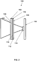
FIG. 2 is a cross-sectional view of the assembly illustrated inFIG. 1 along line 2- 2; -
FIG. 3 is a side elevational view of an apparatus for manufacturing the assembly illustrated inFIG. 1 ; -
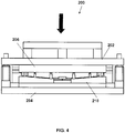
FIG. 4 is a side elevational view of the apparatus illustrated inFIG. 3 with an upper die set and a lower die set closed; and -
FIG. 5 is a flowchart showing steps in the manufacture of the assembly illustrated inFIG. 1 ; - The present invention provides an apparatus and a method for illuminating a circuit board such that the light traveling through the circuit board does not substantially change color or lose its intensity. Also, the apparatus and method may be used with lead free solder and two-sided traces.
- Turning to
FIGS. 1 and2 , anassembly 100 is shown. Theassembly 100 includes asubstrate 102 with afirst surface 104 and asecond surface 106 opposite thefirst surface 104, aflexible layer 108 with afirst surface 110 and asecond surface 112 opposite thefirst surface 110, and anadhesive 114 between thesubstrate 102 and theflexible layer 108. In the embodiment shown, theassembly 100 is illuminated by alight source 116. The depictedlight source 116 is mounted to an illumination printedcircuit board 118. However, in other embodiments, thelight source 116 need not be mounted to an illumination printedcircuit board 118. Also, thelight source 116 can be an incandescent bulb, fluorescent bulb, light emitting diode, combinations of the aforementioned, or any other device that provides light or illumination. - For the sake of simplifying the description, the invention is described in reference to an embodiment where the
assembly 100 provides asubstrate 102 with which a user interacts. The user interactions on thefirst surface 104 of thesubstrate 102 actuate one or more capacitive or field effect devices disposed on theflexible layer 108 adjacent to thesubstrate 102. Thefirst surface 104 of thesubstrate 102 can include indicia such as words, diagrams, pictures, signs, and other indicators that can be imprinted, printed, etched, sculpted, painted, adhered, or other mated to thefirst surface 104. The user touches thefirst surface 104 near one or more of the capacitive or field effect devices, and the touch on thefirst surface 104 actuates the one or more capacitive or field effect devices disposed on theflexible layer 108. Such anassembly 100 can be used, for example, in an automobile to control or manipulate one or more functions of a system of the automobile. For example, thefirst surface 104 of thesubstrate 102 can have indicia for temperature control and theflexible layer 108 can have a capacitive device associated with the indicia for temperature control. Thelight source 116 can emit light through thesubstrate 102 and theflexible layer 108 and thus illuminate the indicia for temperature control on thefirst surface 104 of thesubstrate 102 and the associated capacitive device on theflexible layer 108 such that the user can visually perceive the indicia and the associated capacitive device. Thus, when the user touches thefirst surface 104 near the indicia for temperature control, the associated capacitive device on theflexible layer 108 is actuated and sends a signal that changes the temperature setting of an air conditioning system or heating system. However, the invention is not limited to such an embodiment and can be applied to anyassembly 100 that requires a substantially transparent or translucentflexible layer 108 coupled to asubstrate 102. - The
substrate 102 can provide mechanical support, an interface for a user, asurface 104 for decorative features, combinations of the aforementioned, or some other similar function. Although thesubstrate 102 is shown as being a generally flat board, thesubstrate 102 can have an irregular shape or contour. Thesecond surface 106 of the substrate may be mated to theflexible layer 108. Thesubstrate 102 can be made from plastic, thermoset, thermoset polyethylene, thermoplastic such as acrylic or acrylonitrile butadiene styrene, thermoplastic polymer such as polycarbonate, thermoplastic fluoropolymer, fluorocarbon-based polymer, polyethylene, polyvinyl chlorides, polyvinylidene fluoride, ethylene tetrafluoroethylene, silicone, glass, combinations of the aforementioned, or any other rigid material that is substantially transparent, translucent, or allows some portion of light to pass. In the embodiment shown, thesubstrate 102 is made from polycarbonate and acrylonitrile butadiene styrene (ABS). - The
flexible layer 108 provides asurface flexible layer 108 is flexible so that it can substantially match the shape and contour of thesubstrate 102. Theflexible layer 108 is also substantially transparent, translucent, or white to allow at least a portion of light to travel through it with substantially no change in the color or intensity of the light. In the embodiment shown, components are mounted on thesurface flexible layer 108 can be made from a polytetrafluoroethylene (PTFE) film, plastic, thermoset, thermoset polyethylene, thermoplastic such as acrylic or acrylonitrile butadiene styrene, thermoplastic polymer such as polycarbonate, thermoplastic fluoropolymer, fluorocarbon-based polymer, polyethylene, polyvinyl chlorides, polyvinylidene fluoride, ethylene tetrafluoroethylene, silicone, constructs containing glass or glass fibers, combinations of the aforementioned, or any other rigid material that is substantially transparent or translucent and flexible enough to conform to the shape and contours of the substrate. In the embodiment shown, theflexible layer 108 is made from thin, flexible FR408 with substantially no ultraviolet inhibitors or doping. FR408 is made from resin-reinforced glass fibers and is commercially available from Isola Global. Also, aflexible layer 108 with a thickness of approximately 0.08 mm provides optimal characteristics for light transmission and flexibility for matching the contours of thesubstrate 102. - The adhesive 114 couples the
substrate 102 and theflexible layer 108. The adhesive 114 can be substantially transparent, translucent, or allow some portion of light to pass so that, when the adhesive 114 is used to mate thesubstrate 102 and theflexible layer 104, the adhesive 114 allows at least some portion of light to pass without substantially changing the color or intensity of the light. Furthermore, the adhesive 114 can form a thin mating that is more reliable and more uniform than a mating formed from pressure sensitive tape and adhesives. The adhesive 114 can be a solvent-free plastic adhesive (such as acrylated urethane commercially available as DYMAX 3069), a solvent-free glob top chip encapsulant (such as modified urethane commercially available as the DYMAX 9001 series of adhesives), modified acrylate (such as those commercially available as the LOCTITE 3492 series of adhesives or the LOCTITE 3493 series of adhesives), modified acrylic (such as those commercially available as the LOCTITE 3494 series of adhesives), or any other appropriate adhesive that cures substantially transparent or translucent. The adhesive 114 can be an ultraviolet light (UV) or natural light curable adhesive. In an embodiment using UV light curable adhesive, theflexible layer 108 has substantially no UV blocking agent so that UV light can substantially pass through theflexible layer 108 to cause curing of the UV light curable adhesive. In the embodiment shown, the adhesive is a UV or natural light curable adhesive, such as DYMAX 3069, and theflexible layer 108 is made from FR408 with substantially no UV blocking agent. In other embodiments, the adhesive 1 14 can be a heat curable adhesive such as thermoplastic or chemical reaction curable adhesive such as polyvinyl acetate, epoxy, polyurethane, cyanoacrylate polymers, polychloroprene, acrylate based polymers, a resin and its corresponding accelerant, and similar adhesives. - Before curing, the adhesive 114 can be disposed on either the
second surface 106 of the substrate or thefirst surface 110 of theflexible layer 108 as a thin, uniform coating. Also, when the adhesive 114 is made from UV or natural light curable adhesive, it substantially prevents formation of air gaps between thesubstrate 102 and theflexible layer 108. Thus, when a capacitive or field effect circuit, device, or sensor is placed on theflexible layer 108, air gaps do not substantially impair the performance of the capacitive or field effect circuit, device, or sensor. - In addition, in the embodiment where the adhesive 114 is a UV or natural light curable adhesive, the adhesive 114 can aid in making the
substrate 102 or theflexible layer 108 more transparent, more translucent, or allow at least some portion of light to pass more readily. If the adhesive 114 has a viscosity so that it allows the adhesive 114 to fill in the texture of thesurface substrate 102 or theflexible layer 108 more transparent, more translucent, or allow some portion of light to pass more readily. Such an adhesive 114 acts as a wetting agent and allows more light to pass through thesubstrate 102 or theflexible layer 108. - The
flexible layer 108 may be connected to the illumination printedcircuit board 118 by an electrical pathway. In the embodiment shown, a flat flexible cable (FFC) connector connects theflexible layer 108 and theillumination circuit board 118. In other embodiments, theflexible layer 108 and theillumination circuit board 118 can be connected by a trace, a wire, a cable, a coaxial cable, a wireless transmission path, combinations of the aforementioned, or any other pathway for signals between two components. - Referring to
FIGS. 3-4 , anapparatus 200 for manufacturing theassembly 100 is shown. Turning toFIG. 3 , theapparatus 200 includes an upper die set 202 and alower die set 204. The terms "upper" and "lower" are not meant to be limiting but are used to describe the relative positions of the components within theapparatus 200. For example, in another embodiment, the die sets 202 and 204 may be oriented laterally so that the die sets 202, 204 are to the right or left of each other or some other orientation. The upper die set 202 can be moved towards or away from the lower die set 204 as indicated by the arrows in the figure. InFIG. 3 , the upper die set 202 and the lower die set 204 are apart from each other. - The upper die set 202 includes a curing
light source 206 and apressure pad 208. The curinglight source 206 emits a light that causes curing of the adhesive 114. The curinglight source 206 can be one or more light emitting diodes, metal halide bulbs, or the like. Thepressure pad 208 presses together thesubstrate 102 and theflexible layer 108 so that theflexible layer 108 conforms to the irregular shape or contours of thesubstrate 102. Thesubstrate 102 and theflexible layer 108 may be disposed in the lower die set 204, and thepressure pad 208 provides substantially uniform pressure to press together thesubstrate 102 and theflexible layer 108 when the upper die set 202 is pressed towards thelower die set 204. In the embodiment shown, thepressure pad 208 is between the curinglight source 206 andlower die set 204. Also, the curinglight source 206 emits light of approximately 6 mW/cm2 and approximately 365 nm to cure the UV light curable adhesive. The depictedpressure pad 208 is a substantially continuous surface. In other embodiments, thepressure pad 208 can formed from a lattice structure or a surface that is not continuous. However, apressure pad 208 formed from a lattice structure is less efficient and forms a less reliable mating of thesubstrate 102 and theflexible layer 108. A latticestructure pressure pad 208 causes a "doming" effect in the adhesive 114 between thesubstrate 102 and theflexible layer 108, and the "doming" effect produces an adhesive 114 with an inconsistent thickness. In an embodiment where the adhesive 114 is a heat curable or chemical reaction curable adhesive, the curinglight source 206 is replaced with a heat source. - The lower die cast 204 includes a
nest 210. Thenest 210 receives thesubstrate 102, the adhesive 1 14, and theflexible layer 108. The adhesive 114 is placed between thesubstrate 102 and theflexible layer 108 so that when the upper die set 202 is pressed towards the lower die set 204, the adhesive 114 is pressed between thesubstrate 102 and theflexible layer 108 so that thesubstrate 102 and theflexible layer 108 are mated. Thenest 210 is shaped to conform to thefirst surface 104 of thesubstrate 102. - Turning to
FIG. 4 , after thesubstrate 102, the adhesive 114, and theflexible layer 108 are placed in thenest 210 of the lower die set 204, the upper die set 202 is pressed towards thelower die set 204. When the upper die set 202 is pressed toward the lower die set 204, thesubstrate 102, the adhesive 1 14, and theflexible layer 108 are pressed together between thepressure pad 208 and thenest 210. Thepressure pad 208 presses together thesubstrate 102, the adhesive 114, and theflexible layer 108 to ensure thatflexible layer 108 substantially conforms to the shape and contour of thesubstrate 102. Thepressure pad 208 also ensures that the adhesive 1 14 is substantially thin, uniform, and has no air gaps. After thesubstrate 102, the adhesive 1 14, and theflexible layer 108 are pressed together, the curinglight source 206 is actuated, and the light emitted from the curinglight source 206 causes curing of the adhesive 114. After the adhesive 114 is substantially cured, the upper die set 202 is moved away from the lower die set 204, and thefinished assembly 100 is removed from thenest 210. - Referring to
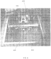
FIG 5 , steps in a method 300 of manufacturing theassembly 100 are shown. The steps shown are not meant to be limiting to the invention. Instead, the illustrated steps show one exemplary embodiment of the method 300 of manufacturing theassembly 100. One or more of the steps may be omitted in other embodiments, or the steps may be performed in an order different from the one shown inFIG 5 . In step 302, an adhesive stencil fixture is provided. In step 304, aflexible layer 108 is placed on the adhesive stencil fixture . In the exemplary embodiment, theflexible layer 108 includes components to form a circuit. - In step 306, an adhesive stencil is placed over the
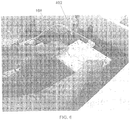
flexible layer 108 and the adhesive stencil fixture . Theadhesive stencil 404 has one or more apertures that expose the underlyingflexible layer 108 so thatuncured adhesive 114 is applied to only predetermined portions of theflexible layer 108 exposed by the apertures . Also, an applicator is placed over the adhesive stencil. In step 308, the applicator moves over the adhesive stencil and applies uncured adhesive 114 to the adhesive stencil. As the applicator applies theuncured adhesive 114 to the adhesive stencil, theuncured adhesive 114 is applied to only the portions of theflexible layer 108 exposed by the apertures . In step 310, the applicator and the adhesive stencil are removed. Thus,uncured adhesive 114 is disposed on portions of theflexible layer 108, with theflexible layer 108 disposed in the adhesive stencil fixture . - In step 312, the
flexible layer 108 withuncured adhesive 114 is removed from the adhesive stencil fixture . In step 314, thesubstrate 102 is disposed in thenest 210 of thelower die set 204. In step 316, theflexible layer 108 withuncured adhesive 114 is disposed on thesubstrate 102 such that theuncured adhesive 114 is between portions of theflexible layer 108 and thesubstrate 102, . In step 320, the upper die set 202 is pressed towards thelower die set 204. In step 320, as the upper die set 202 is pressed towards the lower die set 204, the curinglight source 206 is actuated. The light from the curinglight source 206 causes curing of the uncured adhesive 1 14. In step 322, the upper die set 202 is moved away from the lower die set 204 when theuncured adhesive 114 is substantially cured. - While particular embodiments have been chosen to illustrate the invention, it will be understood by those skilled in the art that various changes and modifications can be made therein without departing from the scope of the invention as defined in the appended claims.
Claims (13)
- An assembly (100), the assembly comprising:
a circuit board having an illumination device for outputting light characterized by a color and an intensity;a substrate (102) with a first surface (104) and a second surface (106) opposite the first surface, wherein the substrate allows some portion of the light to pass through the substrate;a flexible layer (108) with a first surface (110) and a second surface (112) opposite the first surface, wherein the flexible layer substantially conforms to the shape of the substrate, and wherein the flexible layer allows a portion of the light to pass through the first surface and the second surface of the flexible layer, wherein the flexible layer has a thickness such that the light passes through the flexible layer without change to colour or intensity of the light;an electrical pathway for sending and receiving an electrical signal between the circuit board and the flexible layer;an adhesive (114) between and mating the second surface of the substrate and the first surface of the flexible layer, wherein the adhesive has at least a viscosity that allows the adhesive to fill in a texture of at least one of the second surface of the substrate and the first surface of the flexible layer to prevent air gaps, and wherein the adhesive allows a portion of the light to pass through the adhesive without changing the colour or the intensity of the light; andone or more capacitive or field effect devices disposed on the flexible layer (108) configured to be actuated when a user interacts by touching on the first surface (104) of the substrate (102). - The assembly according to claim 1, wherein the flexible layer is transparent.
- The assembly according to claim 1, wherein the flexible layer is translucent.
- The assembly according to claim 1, wherein the flexible layer is white.
- The assembly according to claim 1, wherein the flexible layer has a thickness of approximately 0.08 mm.
- The assembly according to claim 1, wherein the flexible layer comprises a material formed of resin-reinforced glass fibers with no ultraviolet inhibitors or doping.
- The assembly according to claim 1, wherein the adhesive is one of an ultraviolet light curable adhesive, a natural light curable adhesive, and a heat curable adhesive.
- A method of manufacturing an assembly, comprising the steps of:providing a substrate with a first surface and a second surface opposite the first surface, wherein the substrate allows a portion of light to pass through the substrate;providing a flexible layer with a first surface and a second surface opposite the first surface, wherein the flexible layer allows a portion of the light to pass through the first surface and the second surface of the flexible layer, wherein the flexible layer has a thickness such that the light passes through the flexible layer without change to colour or intensity of the light, and wherein the flexible layer substantially conforms to the shape of the substrate;disposing an adhesive on at least one of the second surface of the substrate and the first surface of the flexible layer without air gaps, wherein the adhesive allows a portion of the light to pass through the adhesive;filling in a texture of at least one of the second surface of the substrate and the first surface of the flexible layer with the adhesive;pressing together the substrate, the adhesive, and the flexible layer;providing one or more capacitive or field effect devices disposed on the flexible layer (108) configured to be actuated when a user interacts by touching on the first surface (104) of the substrate (102); andconnecting a circuit board having an illumination device to the flexible layer with an electrical pathway for sending and receiving an electrical signal between the circuit board and the flexible layer.
- The method of manufacturing the assembly according to claim 8, wherein the adhesive is at least one of an ultraviolet light curable adhesive, a natural light curable adhesive, and a heat curable adhesive.
- The method of manufacturing the assembly according to claim 9, further comprising the step of curing the adhesive with ultraviolet light.
- The method of manufacturing the assembly according to claim 10, wherein the step of curing the adhesive with ultraviolet light further comprises emitting ultraviolet light through the substrate to cause curing of the adhesive.
- The method of manufacturing the assembly according to claim 11, wherein the step of providing the flexible layer further comprises providing the flexible layer with a white colour.
- The method of manufacturing the assembly according to claim 11, wherein the step of providing the flexible layer further comprises forming the flexible layer from a material formed of resin-reinforced glass fibers with no ultraviolet inhibitors or doping.
Applications Claiming Priority (2)
| Application Number | Priority Date | Filing Date | Title |
|---|---|---|---|
| US23226309P | 2009-08-07 | 2009-08-07 | |
| PCT/US2009/066149 WO2011016817A1 (en) | 2009-08-07 | 2009-11-30 | Assembly and method for illuminating through a circuit board |
Publications (3)
| Publication Number | Publication Date |
|---|---|
| EP2462788A1 EP2462788A1 (en) | 2012-06-13 |
| EP2462788A4 EP2462788A4 (en) | 2013-05-29 |
| EP2462788B1 true EP2462788B1 (en) | 2019-05-15 |
Family
ID=43535043
Family Applications (1)
| Application Number | Title | Priority Date | Filing Date |
|---|---|---|---|
| EP09848136.9A Not-in-force EP2462788B1 (en) | 2009-08-07 | 2009-11-30 | Assembly and method for illuminating through a circuit board |
Country Status (6)
| Country | Link |
|---|---|
| US (1) | US20110033668A1 (en) |
| EP (1) | EP2462788B1 (en) |
| JP (1) | JP5742035B2 (en) |
| KR (2) | KR20130051430A (en) |
| CA (1) | CA2770386A1 (en) |
| WO (1) | WO2011016817A1 (en) |
Families Citing this family (3)
| Publication number | Priority date | Publication date | Assignee | Title |
|---|---|---|---|---|
| DE102010043960A1 (en) * | 2010-11-16 | 2012-05-16 | Lisa Dräxlmaier GmbH | Functional soft-touch layers on interior components |
| DE102017222957A1 (en) * | 2017-12-15 | 2019-06-19 | Benecke-Kaliko Ag | Component with translucent, shape-changing surface |
| JP7193142B2 (en) * | 2019-11-26 | 2022-12-20 | 国立大学法人 東京大学 | Information processing equipment |
Family Cites Families (18)
| Publication number | Priority date | Publication date | Assignee | Title |
|---|---|---|---|---|
| JPS625344U (en) * | 1985-06-21 | 1987-01-13 | ||
| US7075501B1 (en) * | 1990-12-31 | 2006-07-11 | Kopin Corporation | Head mounted display system |
| WO2001057833A1 (en) * | 2000-02-01 | 2001-08-09 | Mitsui Chemicals Inc. | Filter for displaying, display unit and production method therefor |
| US6944018B2 (en) * | 2001-05-07 | 2005-09-13 | Touchsensor Technologies, Llc | Control system input apparatus and method |
| JP2003003777A (en) * | 2001-06-27 | 2003-01-08 | Central Motor Co Ltd | Elevating ladder with enclosure |
| TW577242B (en) * | 2002-08-19 | 2004-02-21 | Ritdisplay Corp | Organic light emitting panel and method of manufacturing the same |
| DE10253420A1 (en) * | 2002-11-15 | 2004-06-03 | Honeywell B.V. | Printed circuit board with display element |
| DE602004029661D1 (en) * | 2003-03-27 | 2010-12-02 | E Ink Corp | ELECTROOPTICAL MODULES |
| JP2005031790A (en) * | 2003-07-08 | 2005-02-03 | Alps Electric Co Ltd | Mounting method for capacitance input sensor and electronic device |
| US20050073507A1 (en) * | 2003-10-06 | 2005-04-07 | Richter Paul J. | Touch input sensing device |
| US7836588B2 (en) * | 2006-07-06 | 2010-11-23 | Ideon Llc | Method for fabricating an electronic device |
| JP2008033777A (en) * | 2006-07-31 | 2008-02-14 | Optrex Corp | Electrode substrate, method for manufacturing the same, display device and method for manufacturing the same |
| TW200835995A (en) * | 2006-10-10 | 2008-09-01 | Cbrite Inc | Electro-optic display |
| US20080124528A1 (en) * | 2006-11-29 | 2008-05-29 | Motorola, Inc. | Printed electronic device and methods of determining the electrical value thereof |
| ITBO20070001A1 (en) * | 2007-01-03 | 2008-07-04 | Selta S R L | FUNCTIONAL PANEL FOR ALFA-NUMERICAL COOKING HOB AND INTEGRATED ALFA-DISPLAY |
| KR101408510B1 (en) * | 2007-05-18 | 2014-06-17 | 삼성전자주식회사 | Flexible substrate for display element and display element using the same |
| JP2009003518A (en) * | 2007-06-19 | 2009-01-08 | Micro Gijutsu Kenkyusho:Kk | Capacitive touch panel and manufacturing method thereof |
| US7933123B2 (en) * | 2008-04-11 | 2011-04-26 | Apple Inc. | Portable electronic device with two-piece housing |
-
2009
- 2009-11-30 WO PCT/US2009/066149 patent/WO2011016817A1/en not_active Ceased
- 2009-11-30 KR KR1020127004051A patent/KR20130051430A/en not_active Ceased
- 2009-11-30 US US12/628,114 patent/US20110033668A1/en not_active Abandoned
- 2009-11-30 KR KR1020177032515A patent/KR101901347B1/en not_active Expired - Fee Related
- 2009-11-30 EP EP09848136.9A patent/EP2462788B1/en not_active Not-in-force
- 2009-11-30 CA CA2770386A patent/CA2770386A1/en not_active Abandoned
- 2009-11-30 JP JP2012523590A patent/JP5742035B2/en not_active Expired - Fee Related
Non-Patent Citations (1)
| Title |
|---|
| None * |
Also Published As
| Publication number | Publication date |
|---|---|
| EP2462788A4 (en) | 2013-05-29 |
| JP5742035B2 (en) | 2015-07-01 |
| KR20130051430A (en) | 2013-05-20 |
| WO2011016817A1 (en) | 2011-02-10 |
| KR101901347B1 (en) | 2018-09-21 |
| KR20170127573A (en) | 2017-11-21 |
| EP2462788A1 (en) | 2012-06-13 |
| US20110033668A1 (en) | 2011-02-10 |
| JP2013501972A (en) | 2013-01-17 |
| CA2770386A1 (en) | 2011-02-10 |
Similar Documents
| Publication | Publication Date | Title |
|---|---|---|
| KR102153775B1 (en) | Method for manufacturing electronic products, related arrangement and product | |
| JP7113027B2 (en) | Electronic assembly manufacturing method and electronic assembly | |
| JP7255603B2 (en) | Multilayer structures for electronic devices and related manufacturing methods | |
| JP2005108844A (en) | Electroluminescent lamp unit | |
| JP2003532982A (en) | Electroluminescent lamp device and method of manufacturing the same | |
| CN111399702B (en) | In-film electronic structure with luminous indication and touch control functions and manufacturing method thereof | |
| CN104421715B (en) | A lighting device and corresponding method | |
| CN110475430B (en) | Multi-resin overmolding for printed circuit board electronics and light guides | |
| US20110033668A1 (en) | Apparatus and method for illuminating through a circuit board | |
| EP1837923A3 (en) | LED backlight unit without printed circuit board and method of manufacturing the same | |
| JPWO2016047229A1 (en) | Light emitting device | |
| CN102713700A (en) | Light source and light conductor coupling | |
| CN104870233A (en) | Illuminated vehicle interior component | |
| JP7288286B1 (en) | Electronic device manufacturing method | |
| CN110475431A (en) | It coats and moulds for more resins of printed circuit board electronic device and light guide | |
| CN223672002U (en) | Smart surface encapsulation structures, smart surface structures, electronic devices and vehicles | |
| CN222088233U (en) | A flexible light-transmitting display module | |
| CN205158816U (en) | LED display module | |
| CN112483922A (en) | Closed LED lamp strip manufactured by light-transmitting adhesive film and manufacturing method thereof | |
| CN109917636A (en) | A kind of smartwatch adjusting light transmittance | |
| JPH1140350A (en) | Dispersion type electroluminescence element and illumination unit using the same |
Legal Events
| Date | Code | Title | Description |
|---|---|---|---|
| PUAI | Public reference made under article 153(3) epc to a published international application that has entered the european phase |
Free format text: ORIGINAL CODE: 0009012 |
|
| 17P | Request for examination filed |
Effective date: 20120307 |
|
| AK | Designated contracting states |
Kind code of ref document: A1 Designated state(s): AT BE BG CH CY CZ DE DK EE ES FI FR GB GR HR HU IE IS IT LI LT LU LV MC MK MT NL NO PL PT RO SE SI SK SM TR |
|
| DAX | Request for extension of the european patent (deleted) | ||
| A4 | Supplementary search report drawn up and despatched |
Effective date: 20130502 |
|
| RIC1 | Information provided on ipc code assigned before grant |
Ipc: H05K 1/00 20060101AFI20130424BHEP |
|
| STAA | Information on the status of an ep patent application or granted ep patent |
Free format text: STATUS: EXAMINATION IS IN PROGRESS |
|
| 17Q | First examination report despatched |
Effective date: 20171023 |
|
| RIC1 | Information provided on ipc code assigned before grant |
Ipc: B32B 27/36 20060101ALI20180928BHEP Ipc: H05K 1/00 20060101AFI20180928BHEP Ipc: B32B 27/30 20060101ALI20180928BHEP Ipc: B32B 27/28 20060101ALI20180928BHEP Ipc: B32B 7/12 20060101ALI20180928BHEP Ipc: B32B 27/32 20060101ALI20180928BHEP Ipc: B32B 27/08 20060101ALI20180928BHEP |
|
| GRAP | Despatch of communication of intention to grant a patent |
Free format text: ORIGINAL CODE: EPIDOSNIGR1 |
|
| STAA | Information on the status of an ep patent application or granted ep patent |
Free format text: STATUS: GRANT OF PATENT IS INTENDED |
|
| INTG | Intention to grant announced |
Effective date: 20181127 |
|
| GRAS | Grant fee paid |
Free format text: ORIGINAL CODE: EPIDOSNIGR3 |
|
| GRAA | (expected) grant |
Free format text: ORIGINAL CODE: 0009210 |
|
| STAA | Information on the status of an ep patent application or granted ep patent |
Free format text: STATUS: THE PATENT HAS BEEN GRANTED |
|
| AK | Designated contracting states |
Kind code of ref document: B1 Designated state(s): AT BE BG CH CY CZ DE DK EE ES FI FR GB GR HR HU IE IS IT LI LT LU LV MC MK MT NL NO PL PT RO SE SI SK SM TR |
|
| REG | Reference to a national code |
Ref country code: CH Ref legal event code: EP Ref country code: GB Ref legal event code: FG4D |
|
| REG | Reference to a national code |
Ref country code: DE Ref legal event code: R096 Ref document number: 602009058407 Country of ref document: DE |
|
| REG | Reference to a national code |
Ref country code: IE Ref legal event code: FG4D |
|
| REG | Reference to a national code |
Ref country code: NL Ref legal event code: MP Effective date: 20190515 |
|
| RAP2 | Party data changed (patent owner data changed or rights of a patent transferred) |
Owner name: METHODE ELECTRONICS, INC. |
|
| REG | Reference to a national code |
Ref country code: LT Ref legal event code: MG4D |
|
| PG25 | Lapsed in a contracting state [announced via postgrant information from national office to epo] |
Ref country code: ES Free format text: LAPSE BECAUSE OF FAILURE TO SUBMIT A TRANSLATION OF THE DESCRIPTION OR TO PAY THE FEE WITHIN THE PRESCRIBED TIME-LIMIT Effective date: 20190515 Ref country code: SE Free format text: LAPSE BECAUSE OF FAILURE TO SUBMIT A TRANSLATION OF THE DESCRIPTION OR TO PAY THE FEE WITHIN THE PRESCRIBED TIME-LIMIT Effective date: 20190515 Ref country code: HR Free format text: LAPSE BECAUSE OF FAILURE TO SUBMIT A TRANSLATION OF THE DESCRIPTION OR TO PAY THE FEE WITHIN THE PRESCRIBED TIME-LIMIT Effective date: 20190515 Ref country code: NO Free format text: LAPSE BECAUSE OF FAILURE TO SUBMIT A TRANSLATION OF THE DESCRIPTION OR TO PAY THE FEE WITHIN THE PRESCRIBED TIME-LIMIT Effective date: 20190815 Ref country code: PT Free format text: LAPSE BECAUSE OF FAILURE TO SUBMIT A TRANSLATION OF THE DESCRIPTION OR TO PAY THE FEE WITHIN THE PRESCRIBED TIME-LIMIT Effective date: 20190915 Ref country code: FI Free format text: LAPSE BECAUSE OF FAILURE TO SUBMIT A TRANSLATION OF THE DESCRIPTION OR TO PAY THE FEE WITHIN THE PRESCRIBED TIME-LIMIT Effective date: 20190515 Ref country code: LT Free format text: LAPSE BECAUSE OF FAILURE TO SUBMIT A TRANSLATION OF THE DESCRIPTION OR TO PAY THE FEE WITHIN THE PRESCRIBED TIME-LIMIT Effective date: 20190515 Ref country code: NL Free format text: LAPSE BECAUSE OF FAILURE TO SUBMIT A TRANSLATION OF THE DESCRIPTION OR TO PAY THE FEE WITHIN THE PRESCRIBED TIME-LIMIT Effective date: 20190515 |
|
| PG25 | Lapsed in a contracting state [announced via postgrant information from national office to epo] |
Ref country code: LV Free format text: LAPSE BECAUSE OF FAILURE TO SUBMIT A TRANSLATION OF THE DESCRIPTION OR TO PAY THE FEE WITHIN THE PRESCRIBED TIME-LIMIT Effective date: 20190515 Ref country code: BG Free format text: LAPSE BECAUSE OF FAILURE TO SUBMIT A TRANSLATION OF THE DESCRIPTION OR TO PAY THE FEE WITHIN THE PRESCRIBED TIME-LIMIT Effective date: 20190815 Ref country code: GR Free format text: LAPSE BECAUSE OF FAILURE TO SUBMIT A TRANSLATION OF THE DESCRIPTION OR TO PAY THE FEE WITHIN THE PRESCRIBED TIME-LIMIT Effective date: 20190816 |
|
| REG | Reference to a national code |
Ref country code: AT Ref legal event code: MK05 Ref document number: 1134921 Country of ref document: AT Kind code of ref document: T Effective date: 20190515 |
|
| PG25 | Lapsed in a contracting state [announced via postgrant information from national office to epo] |
Ref country code: AT Free format text: LAPSE BECAUSE OF FAILURE TO SUBMIT A TRANSLATION OF THE DESCRIPTION OR TO PAY THE FEE WITHIN THE PRESCRIBED TIME-LIMIT Effective date: 20190515 Ref country code: DK Free format text: LAPSE BECAUSE OF FAILURE TO SUBMIT A TRANSLATION OF THE DESCRIPTION OR TO PAY THE FEE WITHIN THE PRESCRIBED TIME-LIMIT Effective date: 20190515 Ref country code: SK Free format text: LAPSE BECAUSE OF FAILURE TO SUBMIT A TRANSLATION OF THE DESCRIPTION OR TO PAY THE FEE WITHIN THE PRESCRIBED TIME-LIMIT Effective date: 20190515 Ref country code: EE Free format text: LAPSE BECAUSE OF FAILURE TO SUBMIT A TRANSLATION OF THE DESCRIPTION OR TO PAY THE FEE WITHIN THE PRESCRIBED TIME-LIMIT Effective date: 20190515 Ref country code: CZ Free format text: LAPSE BECAUSE OF FAILURE TO SUBMIT A TRANSLATION OF THE DESCRIPTION OR TO PAY THE FEE WITHIN THE PRESCRIBED TIME-LIMIT Effective date: 20190515 Ref country code: RO Free format text: LAPSE BECAUSE OF FAILURE TO SUBMIT A TRANSLATION OF THE DESCRIPTION OR TO PAY THE FEE WITHIN THE PRESCRIBED TIME-LIMIT Effective date: 20190515 |
|
| REG | Reference to a national code |
Ref country code: DE Ref legal event code: R097 Ref document number: 602009058407 Country of ref document: DE |
|
| PG25 | Lapsed in a contracting state [announced via postgrant information from national office to epo] |
Ref country code: SM Free format text: LAPSE BECAUSE OF FAILURE TO SUBMIT A TRANSLATION OF THE DESCRIPTION OR TO PAY THE FEE WITHIN THE PRESCRIBED TIME-LIMIT Effective date: 20190515 Ref country code: IT Free format text: LAPSE BECAUSE OF FAILURE TO SUBMIT A TRANSLATION OF THE DESCRIPTION OR TO PAY THE FEE WITHIN THE PRESCRIBED TIME-LIMIT Effective date: 20190515 |
|
| PLBE | No opposition filed within time limit |
Free format text: ORIGINAL CODE: 0009261 |
|
| STAA | Information on the status of an ep patent application or granted ep patent |
Free format text: STATUS: NO OPPOSITION FILED WITHIN TIME LIMIT |
|
| PG25 | Lapsed in a contracting state [announced via postgrant information from national office to epo] |
Ref country code: TR Free format text: LAPSE BECAUSE OF FAILURE TO SUBMIT A TRANSLATION OF THE DESCRIPTION OR TO PAY THE FEE WITHIN THE PRESCRIBED TIME-LIMIT Effective date: 20190515 |
|
| 26N | No opposition filed |
Effective date: 20200218 |
|
| PG25 | Lapsed in a contracting state [announced via postgrant information from national office to epo] |
Ref country code: PL Free format text: LAPSE BECAUSE OF FAILURE TO SUBMIT A TRANSLATION OF THE DESCRIPTION OR TO PAY THE FEE WITHIN THE PRESCRIBED TIME-LIMIT Effective date: 20190515 |
|
| PG25 | Lapsed in a contracting state [announced via postgrant information from national office to epo] |
Ref country code: SI Free format text: LAPSE BECAUSE OF FAILURE TO SUBMIT A TRANSLATION OF THE DESCRIPTION OR TO PAY THE FEE WITHIN THE PRESCRIBED TIME-LIMIT Effective date: 20190515 |
|
| REG | Reference to a national code |
Ref country code: CH Ref legal event code: PL |
|
| PG25 | Lapsed in a contracting state [announced via postgrant information from national office to epo] |
Ref country code: LU Free format text: LAPSE BECAUSE OF NON-PAYMENT OF DUE FEES Effective date: 20191130 Ref country code: CH Free format text: LAPSE BECAUSE OF NON-PAYMENT OF DUE FEES Effective date: 20191130 Ref country code: LI Free format text: LAPSE BECAUSE OF NON-PAYMENT OF DUE FEES Effective date: 20191130 Ref country code: MC Free format text: LAPSE BECAUSE OF FAILURE TO SUBMIT A TRANSLATION OF THE DESCRIPTION OR TO PAY THE FEE WITHIN THE PRESCRIBED TIME-LIMIT Effective date: 20190515 |
|
| REG | Reference to a national code |
Ref country code: BE Ref legal event code: MM Effective date: 20191130 |
|
| GBPC | Gb: european patent ceased through non-payment of renewal fee |
Effective date: 20191130 |
|
| PG25 | Lapsed in a contracting state [announced via postgrant information from national office to epo] |
Ref country code: IE Free format text: LAPSE BECAUSE OF NON-PAYMENT OF DUE FEES Effective date: 20191130 Ref country code: FR Free format text: LAPSE BECAUSE OF NON-PAYMENT OF DUE FEES Effective date: 20191130 Ref country code: GB Free format text: LAPSE BECAUSE OF NON-PAYMENT OF DUE FEES Effective date: 20191130 |
|
| PG25 | Lapsed in a contracting state [announced via postgrant information from national office to epo] |
Ref country code: BE Free format text: LAPSE BECAUSE OF NON-PAYMENT OF DUE FEES Effective date: 20191130 |
|
| PG25 | Lapsed in a contracting state [announced via postgrant information from national office to epo] |
Ref country code: CY Free format text: LAPSE BECAUSE OF FAILURE TO SUBMIT A TRANSLATION OF THE DESCRIPTION OR TO PAY THE FEE WITHIN THE PRESCRIBED TIME-LIMIT Effective date: 20190515 |
|
| PG25 | Lapsed in a contracting state [announced via postgrant information from national office to epo] |
Ref country code: IS Free format text: LAPSE BECAUSE OF FAILURE TO SUBMIT A TRANSLATION OF THE DESCRIPTION OR TO PAY THE FEE WITHIN THE PRESCRIBED TIME-LIMIT Effective date: 20190915 |
|
| PG25 | Lapsed in a contracting state [announced via postgrant information from national office to epo] |
Ref country code: MT Free format text: LAPSE BECAUSE OF FAILURE TO SUBMIT A TRANSLATION OF THE DESCRIPTION OR TO PAY THE FEE WITHIN THE PRESCRIBED TIME-LIMIT Effective date: 20190515 Ref country code: HU Free format text: LAPSE BECAUSE OF FAILURE TO SUBMIT A TRANSLATION OF THE DESCRIPTION OR TO PAY THE FEE WITHIN THE PRESCRIBED TIME-LIMIT; INVALID AB INITIO Effective date: 20091130 |
|
| PG25 | Lapsed in a contracting state [announced via postgrant information from national office to epo] |
Ref country code: MK Free format text: LAPSE BECAUSE OF FAILURE TO SUBMIT A TRANSLATION OF THE DESCRIPTION OR TO PAY THE FEE WITHIN THE PRESCRIBED TIME-LIMIT Effective date: 20190515 |
|
| P01 | Opt-out of the competence of the unified patent court (upc) registered |
Effective date: 20230629 |
|
| PGFP | Annual fee paid to national office [announced via postgrant information from national office to epo] |
Ref country code: DE Payment date: 20231003 Year of fee payment: 15 |
|
| REG | Reference to a national code |
Ref country code: DE Ref legal event code: R119 Ref document number: 602009058407 Country of ref document: DE |
|
| PG25 | Lapsed in a contracting state [announced via postgrant information from national office to epo] |
Ref country code: DE Free format text: LAPSE BECAUSE OF NON-PAYMENT OF DUE FEES Effective date: 20250603 |