EP2458702B1 - Eigensicherer Gleichspannungswandler - Google Patents
Eigensicherer Gleichspannungswandler Download PDFInfo
- Publication number
- EP2458702B1 EP2458702B1 EP10192831.5A EP10192831A EP2458702B1 EP 2458702 B1 EP2458702 B1 EP 2458702B1 EP 10192831 A EP10192831 A EP 10192831A EP 2458702 B1 EP2458702 B1 EP 2458702B1
- Authority
- EP
- European Patent Office
- Prior art keywords
- voltage
- converter
- input
- supply voltage
- output
- Prior art date
- Legal status (The legal status is an assumption and is not a legal conclusion. Google has not performed a legal analysis and makes no representation as to the accuracy of the status listed.)
- Not-in-force
Links
- 230000007423 decrease Effects 0.000 claims description 6
- 239000011810 insulating material Substances 0.000 claims description 2
- 238000001514 detection method Methods 0.000 description 6
- 230000001419 dependent effect Effects 0.000 description 4
- 238000010586 diagram Methods 0.000 description 2
- 238000005259 measurement Methods 0.000 description 2
- 230000002787 reinforcement Effects 0.000 description 2
- 230000003247 decreasing effect Effects 0.000 description 1
- 230000009977 dual effect Effects 0.000 description 1
- 239000002360 explosive Substances 0.000 description 1
- 238000013021 overheating Methods 0.000 description 1
- 239000004065 semiconductor Substances 0.000 description 1
- 229920003002 synthetic resin Polymers 0.000 description 1
- 239000000057 synthetic resin Substances 0.000 description 1
- 238000004804 winding Methods 0.000 description 1
Images

Classifications
-
- H—ELECTRICITY
- H02—GENERATION; CONVERSION OR DISTRIBUTION OF ELECTRIC POWER
- H02H—EMERGENCY PROTECTIVE CIRCUIT ARRANGEMENTS
- H02H9/00—Emergency protective circuit arrangements for limiting excess current or voltage without disconnection
- H02H9/008—Intrinsically safe circuits
-
- H—ELECTRICITY
- H02—GENERATION; CONVERSION OR DISTRIBUTION OF ELECTRIC POWER
- H02H—EMERGENCY PROTECTIVE CIRCUIT ARRANGEMENTS
- H02H7/00—Emergency protective circuit arrangements specially adapted for specific types of electric machines or apparatus or for sectionalised protection of cable or line systems, and effecting automatic switching in the event of an undesired change from normal working conditions
- H02H7/10—Emergency protective circuit arrangements specially adapted for specific types of electric machines or apparatus or for sectionalised protection of cable or line systems, and effecting automatic switching in the event of an undesired change from normal working conditions for converters; for rectifiers
- H02H7/12—Emergency protective circuit arrangements specially adapted for specific types of electric machines or apparatus or for sectionalised protection of cable or line systems, and effecting automatic switching in the event of an undesired change from normal working conditions for converters; for rectifiers for static converters or rectifiers
- H02H7/1213—Emergency protective circuit arrangements specially adapted for specific types of electric machines or apparatus or for sectionalised protection of cable or line systems, and effecting automatic switching in the event of an undesired change from normal working conditions for converters; for rectifiers for static converters or rectifiers for DC-DC converters
Definitions
- the invention relates to a DC-DC converter, which converts a supply voltage into an output voltage while receiving an input current, with a power limiting circuit comprising a comparator to which a voltage proportional to the input current is supplied and the output thereof with a circuit for switching off the DC-DC converter connected is.
- a DC-DC converter also called DC / DC converter, converts an input-side supply voltage into a mostly constant output-side DC voltage.
- DC / DC converter converts an input-side supply voltage into a mostly constant output-side DC voltage.
- an inductance controlled by a controlled switch can be in galvanic connection with the output side.
- transformers are used, with the current being clocked by a primary winding by means of a controlled switch.
- the drive circuit includes, for example, a pulse width modulator (PWM) whose duty cycle for the purpose of control, for example, to constant output voltage can be changed.
- PWM pulse width modulator
- Power limiting circuits which monitor the current received by the DC-DC converter to be protected. Such a circuit causes a current limitation, by the shutdown of the DC-DC converter is achieved upon reaching a maximum allowable current. By means of a specified for the DC-DC converter maximum supply voltage thus results in the limitation to a maximum allowable power input.
- the maximum possible supply voltage is therefore used in the prior art for the assessment of the power consumption or power loss, because usually no measurement of the supply voltage takes place.
- a constant voltage is applied to a reference input of a comparator.
- the comparator is a running comparison with a voltage drop in current sense resistors through which flows the input current of the DC-DC converter. As soon as the voltage drop exceeds the constant voltage, the DC-DC converter is switched off.
- a DC-DC converter is known in which also overcurrent limiting is provided to prevent overheating.
- the DC-DC converter has an arrangement with a comparator, to whose non-inverting input a voltage proportional to the input current is applied. This voltage is compared with a threshold and the DC-DC converter is turned off when it is exceeded.
- the invention has for its object to provide an improvement over the prior art for a DC-DC converter of the type mentioned. According to the invention this object is achieved by a DC-DC converter with a power limitation according to claim 1.
- Advantageous embodiments are specified in subclaims.
- a reference voltage is applied to a reference input of the comparator, which decreases as the supply voltage increases and which increases as the supply voltage decreases.
- the circuit takes advantage of the fact that DC-DC converter with higher supply voltage have a lower power consumption.
- the non-constant reference voltage causes the maximum permissible input current to increase when the supply voltage drops.
- the maximum allowable input current is limited to a low value when the input side supply voltage reaches a maximum value.
- the measure according to the invention represents an advantage.
- a corresponding standard for intrinsically safe devices provides for maximum possible power losses.
- a certain level of protection for example "ib" can be predetermined.
- variable reference voltage By the variable reference voltage is taken into account that in a DC-DC converter, the maximum power consumption does not occur at a maximum of the supply voltage.
- the limitation of the current thus continues to lead to a reliable limitation of a limited power loss, even if the maximum possible supply voltage is not used for the assessment of power consumption or power loss.
- the maximum allowable power loss is reduced while maintaining the transferable power.
- the new converter thus has a reduced volume at the same level of protection of intrinsic safety or the transmittable power increases at a constant volume.
- an intrinsically safe DC-DC converter is encapsulated with a suitable insulating material, for example by means of a synthetic resin. This provides additional protection against sparking as a result of an overheated or overloaded component of the DC-DC converter.
- An advantageous embodiment provides that the voltage applied to the reference input of the comparator reference voltage is formed as an output signal of a differential amplifier and that the differential amplifier as the first input signal proportional to the supply voltage and voltage as a second input signal, a constant voltage are supplied.
- the first input signal is derived from the supply voltage by means of a voltage divider.
- a first voltage divider and a second voltage divider are applied to the supply voltage.
- the output of the first voltage divider is on the one hand connected to the reference input of the comparator and on the other hand connected via a transistor with an additional resistor to the output of the second voltage divider.
- a current flow is controlled, which flows from the voltage potential at the output of the first voltage divider to a reference potential. With increasing supply voltage, this controlled current flow increases, so that the voltage potential at the output of the first voltage divider and thus the reference voltage drops.
- the invention relates to a DC-DC converter according to claim 1.
- Advantageous embodiments are defined in the dependent claims.
- a circuit 4 for forming a dependent of the supply voltage 1 reference signal Ua is connected directly and via a voltage divider 2 to the supply voltage 1.
- the voltage Ue1 at the output of the voltage divider 2 is supplied as a first input signal to a differential amplifier 7 ( Fig. 1 ).
- a differential amplifier 7 At a second input of the differential amplifier 7 is applied as a second input signal to a constant voltage Ue2. This is derived by means of a suitable circuit from the supply voltage 1, for example by means of a Zener diode.
- the output signal of the differential amplifier 7 is fed to the reference input of a comparator 5 as a reference voltage Ua.
- a second input of the comparator 5 is connected to the output of a current detection 3.
- This current detection 3 monitors the input current received by the DC-DC converter. For example, the current detection 3 supplies the voltage drop by current sense resistors through which the input current of the DC-DC converter flows.
- the comparator 5 continuously compares the two voltages at the two inputs. As soon as the measurement voltage supplied by the current detection 3 reaches the reference voltage Ua, the output of the comparator tilts and a downstream circuit 6 for switching off the DC-DC converter is activated.
- the first input is the voltage Ue1 proportional to the supply voltage 1 and the second input is the constant voltage Ue2.
- An increasing first voltage Ue1 causes a falling reference voltage Ua.
- the present as the output signal of the differential amplifier 7 reference voltage Ua thus decreases with increasing supply voltage 1 and increases with decreasing supply voltage.
- the first voltage Ue1 at the output of the voltage divider 2 and the constant voltage Ue2 are to be preset in such a way that the reference voltage Ua present at the output of the differential amplifier 7 is suitable for comparison with the measuring voltage from the current detection 3.
- the dependent of the supply voltage 1 reference voltage Ua determines the maximum allowable input current of the DC-DC converter. This maximum permissible input current must at the time of reaching it with the actually occurring supply voltage 1 result in a power consumption, which is with sufficient certainty below the maximum allowable power consumption.
- the selected security depends on a specified level of protection for intrinsically safe devices.
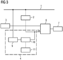
- a current controlled by the transistor 10 influences the voltage potential present at the output of a first voltage divider 2.
- a control voltage of the transistor 10 which is proportional to the supply voltage 1 is available via a second voltage divider 9. If the supply voltage 1 increases, so does the control voltage, whereby the current flow through the transistor 10 increases and the voltage potential at the output of the first voltage divider 2 drops.
- This voltage potential 2 determines the reference voltage Ua at the reference input of the comparator 6. With increasing supply voltage 1, therefore, the decreases Reference voltage Ua. Conversely, the reference voltage Ua increases as soon as the supply voltage 1 drops.
- the second input of the comparator 6 is again connected to the output of the current detection 3. As soon as the output measuring voltage reaches the value of the reference voltage Ua, the output signal of the comparator 6 tilts and a subsequent switching circuit 7 for switching off the DC-DC converter is activated.
- a temperature class for example T4 with a maximum surface temperature of 135 ° C according to IEC 60079-0, chapter 5.3.2.2
- a protection of the DC-DC converter offers a protection of the DC-DC converter.
- integrated temperature sensors would possibly prevent an over-temperature, but such sensors respond with a delay to punctiform overtemperatures of individual components, such as switching transistors.
- the power limitation of the present invention responds without any time delay as soon as the input current reaches the predetermined limit value (determined by the reference voltage) that is dependent on the supply voltage 1.
- An overtemperature, e.g. The switching transistors is better controlled by the present power limitation than by the consideration of the input current at a maximum possible supply voltage according to the prior art.
- the Maximum power loss in the resistors which are located after an output fuse of the boost converter, meaningfully limited.
- these resistors are also protected from overtemperature.
Landscapes
- Engineering & Computer Science (AREA)
- Power Engineering (AREA)
- Dc-Dc Converters (AREA)
Description
- Die Erfindung betrifft einen Gleichspannungswandler, welcher eine Versorgungsspannung in eine Ausgangsspannung umwandelt und dabei einen Eingangsstrom aufnimmt, mit einer Leistungsbegrenzungsschaltung, welche einen Komparator umfasst, dem eine zu dem Eingangsstrom proportionale Spannung zugeführt ist und dessen Ausgang mit einem Schaltkreis zur Abschaltung des Gleichspannungswandlers
verbunden ist. - Ein Gleichspannungswandler, auch DC/DC-Wandler genannt, wandelt eine eingangsseitige Versorgungsspannung in eine zumeist konstante ausgangsseitige Gleichspannung um. Zur Umsetzung des Wandlerprinzips sind zahlreiche Topologien bekannt. Dabei kann eine von einem gesteuerten Schalter angesteuerte Induktivität mit der Ausgangsseite in galvanischer Verbindung stehen. Meistens jedoch werden Übertrager verwendet, wobei der Strom durch eine Primärwicklung mittels eines gesteuerten Schalters getaktet wird. Die Ansteuerschaltung enthält beispielsweise einen Pulsbreitenmodulator (PWM), dessen Tastverhältnis zum Zwecke der Regelung, beispielsweise auf konstante Ausgangsspannung, geändert werden kann.
- Leistungsbegrenzungsschaltungen kommen zur Anwendung, um bei Überlasten bzw. im Fehlerfall ein sicheres Abschalten des Gleichspannungswandlers herbeizuführen. Gegebenenfalls ist aus Sicht der Eigensicherheit nach der Norm DIN EN 60079-11 die maximal mögliche Verlustleistung von DC/DC-Wandlern zu beachten. Dieser Teil von IEC 60079 legt die Bestimmungen für die Konstruktion und Prüfung eigensicherer Betriebsmittel, die für die Verwendung in gasexplosionsgefährdeten Bereichen bestimmt sind, sowie für zugehörige Betriebsmittel fest, die für den Anschluss an eigensichere Stromkreise, die in solche Bereiche hineinführen, vorgesehen sind.
- Bekannt sind Leistungsbegrenzungsschaltungen, welche den Strom überwachen, der von dem zu schützenden Gleichspannungswandler aufgenommen wird. Eine solche Schaltung bewirkt eine Strombegrenzung, indem bei Erreichung eines maximal zulässigen Stromes die Abschaltung des Gleichspannungswandlers herbeigeführt wird. Mittels einer für den Gleichspannungswandler festgelegten maximalen Versorgungsspannung ergibt sich somit auch die Begrenzung auf einen maximal zulässigen Leistungseintrag. Die maximal mögliche Versorgungsspannung wird nach dem Stand der Technik deshalb zur Beurteilung der Leistungsaufnahme bzw. Verlustleistung herangezogen, weil in der Regel keine Messung der Versorgungsspannung erfolgt.
- Konkret wird an einen Referenzeingang eines Komparators eine konstante Spannung angelegt. Mittels des Komparators erfolgt ein laufender Vergleich mit einem Spannungsabfall an Strommesswiderständen, durch die der Eingangsstrom des Gleichspannungswandlers fließt. Sobald der Spannungsabfall die Konstantspannung übersteigt, wird der Gleichspannungswandler abgeschaltet.
- Aus der Schrift
EP 0 638 985 A1 ist beispielsweise ein derartiger Gleichspannungswandler bekannt. Bei diesem ist eine Begrenzung des im primärseitigen Hauptstromkreis fließenden Pulsstromes vorgesehen. Dazu werden einerseits mittels einer ersten Anordnung zur Strombegrenzung Einschaltimpulse verkürzt und andererseits mittels einer zweiten Anordnung zur Strombegrenzung Einschaltimpulse unterdrückt. Die Anordnungen zur Strombegrenzung weisen dabei Komparatoren auf, wobei die an den jeweiligen nichtinvertierenden Eingängen anliegenden Spannungen mit einer Bezugsspannung verglichen werden, für welche eine Konstantspannung als Quelle dient. - Aus der Schrift
US 5,297,014 ist ein Gleichspannungswandler bekannt, bei welchem ebenfalls Überstrombegrenzung zur Vermeidung von Überhitzung vorgesehen ist. Dazu weist der Gleichspannungswandler eine Anordnung mit einem Komparator auf, an dessen nichtinvertierenden Eingang eine dem Eingangsstrom proportionale Spannung anliegt. Diese Spannung wird mit einem Schwellwert verglichen und der Gleichspannungswandler abgeschaltet, wenn dieser überschritten wird. - Der Erfindung liegt die Aufgabe zugrunde, für einen Gleichspannungswandler der eingangs genannten Art eine Verbesserung gegenüber dem Stand der Technik anzugeben. Erfindungsgemäß wird diese Aufgabe gelöst durch einen Gleichspannungswandler mit einer Leistungsbegrenzung gemäß Anspruch 1. In Unteransprüchen sind vorteilhafte Ausführungsformen angegeben.
- Dabei liegt an einem Referenzeingang des Komparators eine Referenzspannung an, welche bei steigender Versorgungsspannung sinkt und welche bei sinkender Versorgungsspannung steigt. Dadurch bleibt die maximal mögliche Leistungsaufnahme eines Gleichspannungswandlers auch bei einer schwankenden Versorgungsspannung konstant. Die Schaltung macht sich die Tatsache zunutze, dass Gleichspannungswandler bei höherer Versorgungsspannung eine niedrigere Stromaufnahme aufweisen. Die nicht konstante Referenzspannung bewirkt, dass bei einem Absinken der Versorgungsspannung der maximal zulässige Eingangsstrom ansteigt. Umgekehrt wird der maximal zulässige Eingangsstrom auf einen niedrigen Wert begrenzt, wenn die eingangsseitige Versorgungsspannung einen Maximalwert erreicht.
- Gegenüber bekannten Leistungsbegrenzungen steigt somit die übertragbare Leistung. Oder es ergibt sich bei gleicher übertragbarer Leistung eine deutlich geringere maximal zulässige Leistungsaufnahme, wodurch die Baugröße des Wandlers reduzierbar ist, ohne die Abschaltsicherheit zu beeinträchtigen.
- Insbesondere für einen Gleichspannungswandler, welcher als eigensicheres Gerät ausgebildet ist, stellt die erfindungsgemäße Maßnahme einen Vorteil dar. Wie bereits dargelegt sieht eine entsprechende Norm für eigensichere Geräte maximal mögliche Verlustleistungen vor. Dabei kann beispielsweise ein bestimmtes Schutzniveau (z.B. "ib") vorgegeben sein.
- Durch die variable Referenzspannung wird berücksichtigt, dass bei einem Gleichspannungswandler die maximale Stromaufnahme nicht bei einem Maximum der Versorgungsspannung auftritt. Die Begrenzung des Stromes führt somit weiterhin zu einer verlässlichen Begrenzung einer zu beschränkenden Verlustleistung, auch wenn für die Beurteilung der Leistungsaufnahme bzw. Verlustleistung nicht die maximal mögliche Versorgungsspannung herangezogen wird. Gegenüber bekannten Leistungsbegrenzungen reduziert sich die maximal zulässige Verlustleistung bei gleichbleibender übertragbarer Leistung. Der neue Wandler weist somit bei unverändertem Schutzniveau der Eigensicherheit ein reduziertes Volumen auf oder die übertragbare Leistung erhöht sich bei gleichbleibendem Volumen.
- Günstigerweise wird ein eigensicherer Gleichspannungswandler mit einem geeigneten Isolationsmaterial vergossen, beispielsweise mittels eines Kunstharzes. Damit ist ein zusätzlicher Schutz gegen Funkenbildung infolge eines überhitzten bzw. überlasteten Bauteils des Gleichspannungswandlers gegeben.
- Eine vorteilhafte Ausführungsvariante sieht vor, dass die am Referenzeingang des Komparators anliegende Referenzspannung als Ausgangssignal eines Differenzverstärkers gebildet ist und dass dem Differenzverstärker als erstes Eingangssignal eine zu der Versorgungsspannung proportionale Spannung und als zweites Eingangssignal ein konstante Spannung zugeführt sind. In einfacher Weise ist das erste Eingangssignal mittels eines Spannungsteilers aus der Versorgungsspannung abgeleitet.
- Bei einer anderen vorteilhaften Ausführungsform liegen an der Versorgungsspannung ein erster Spannungsteiler und ein zweiter Spannungsteiler an. Der Ausgang des ersten Spannungsteilers ist dabei einerseits mit dem Referenzeingang des Komparators verbunden und andererseits über einen Transistor mit einem zusätzlichen Widerstand an den Ausgang des zweiten Spannungsteilers geschaltet. Mit dem Transistor wird ein Stromfluss gesteuert, welcher vom Spannungspotenzial am Ausgang des ersten Spannungsteilers zu einem Bezugspotenzial abfließt. Mit steigender Versorgungsspannung steigt auch dieser gesteuerte Stromfluss an, sodass das Spannungspotenzial am Ausgang des ersten Spannungsteilers und somit die Referenzspannung abfällt.
- Die Erfindung bezieht sich auf einen Gleichspannungswandler gemäß Anspruch 1. Vorteilhafte Ausführungsformen sind in den abhängigen Ansprüchen definiert.
- Die Erfindung wird nachfolgend in beispielhafter Weise unter Bezugnahme auf die beigefügten Figuren erläutert. Es zeigen in schematischer Darstellung:
- Fig. 1
- Blockdarstellung einer ersten Ausführungsform
- Fig. 2
- Spannungsverläufe über der Zeit
- Fig. 3
- Blockdarstellung einer zweiten Ausführungsform
- Eine Schaltung 4 zur Bildung eines von der Versorgungsspannung 1 abhängigen Referenzsignals Ua ist direkt und über einen Spannungsteiler 2 an die Versorgungsspannung 1 geschaltet. Dabei ist in einer ersten Ausführungsform die Spannung Ue1 am Ausgang des Spannungsteilers 2 als erstes Eingangssignal einem Differenzverstärker 7 zugeführt (
Fig. 1 ). An einem zweiten Eingang des Differenzverstärkers 7 liegt als zweites Eingangssignal eine konstante Spannung Ue2 an. Diese ist mittels einer geeigneten Schaltung aus der Versorgungsspannung 1 abgeleitet, beispielsweise mittels einer Zenerdiode. - Das Ausgangssignal des Differenzverstärkers 7 ist dem Referenzeingang eines Komparators 5 als Referenzspannung Ua zugeführt. Ein zweiter Eingang des Komparators 5 ist mit dem Ausgang einer Stromerfassung 3 verbunden. Diese Stromerfassung 3 überwacht den Eingangsstrom, welcher von dem Gleichstromwandler aufgenommen wird. Beispielsweise liefert die Stromerfassung 3 den Spannungsabfall durch Strommesswiderstände, durch die der Eingangsstrom des Gleichspannungswandlers fließt.
- Der Komparator 5 vergleicht laufend die beiden Spannungen an den beiden Eingängen. Sobald die von der Stromerfassung 3 gelieferte Messspannung die Referenzspannung Ua erreicht, kippt der Ausgang des Komparators und ein nachgeschalteter Schaltkreis 6 zur Abschaltung des Gleichspannungswandlers wird aktiviert.
- In
Fig. 2 sind die Eingangsspannungen Ue1, Ue2 und die Referenzspannung Ua am Ausgang des Differenzverstärkers 7 über der Zeit t dargestellt. Ohne Verstärkung gilt die Formel:
- Die erste Eingangsgröße ist die zur Versorgungsspannung 1 proportionale Spannung Ue1 und die zweite Eingangsgröße ist die konstante Spannung Ue2. Eine ansteigende erste Spannung Ue1 bewirkt eine abfallende Referenzspannung Ua. Die als Ausgangssignal des Differenzverstärkers 7 vorliegende Referenzspannung Ua sinkt also bei steigender Versorgungsspannung 1 und steigt bei sinkender Versorgungs spannung.
- Die erste Spannung Ue1 am Ausgang des Spannungsteilers 2 und die konstante Spannung Ue2 sind in der Weise vorzugeben, dass die am Ausgang des Differenzverstärkers 7 anliegende Referenzspannung Ua für den Vergleich mit der Messspannung aus der Stromerfassung 3 geeignet ist. Die von der Versorgungsspannung 1 abhängige Referenzspannung Ua bestimmt den maximal zulässigen Eingangsstrom des Gleichstromwandlers. Dieser maximal zulässige Eingangsstrom muss zum Zeitpunkt seines Erreichens mit der dabei tatsächlich auftretenden Versorgungsspannung 1 eine Leistungsaufnahme ergeben, welche mit einer ausreichenden Sicherheit unterhalb der maximal zulässigen Leistungsaufnahme liegt. Die gewählte Sicherheit hängt beispielsweise von einem festgelegten Schutzniveau für eigensichere Geräte ab.
- In einer zweiten Ausführungsform, in
Fig. 3 dargestellt, beeinflusst ein mit dem Transistor 10 gesteuerter Strom das am Ausgang eines ersten Spannungsteilers 2 anliegende Spannungspotenzial. Über einen zweiten Spannungsteiler 9 steht eine zur Versorgungsspannung 1 proportionale Steuerspannung des Transistors 10 zur Verfügung. Steigt die Versorgungsspannung 1 an, steigt auch die Steuerspannung, wodurch der Stromfluss durch den Transistor 10 ansteigt und das Spannungspotenzial am Ausgang des ersten Spannungsteilers 2 abfällt. Dieses Spannungspotenzial 2 bestimmt dabei die Referenzspannung Ua am Referenzeingang des Komparators 6. Bei steigender Versorgungsspannung 1 sinkt demnach die Referenzspannung Ua. Umgekehrt steigt die Referenzspannung Ua an, sobald die Versorgungsspannung 1 sinkt. - Der zweite Eingang des Komparators 6 ist wieder mit dem Ausgang der Stromerfassung 3 verbunden. Sobald die ausgegebene Messspannung den Wert der Referenzspannung Ua errecht, kippt das Ausgangssignal des Komparators 6 und ein nachfolgender Schaltkreis 7 zur Abschaltung des Gleichspannungswandlers wird aktiviert.
- Auch die Vorgabe einer Temperaturklasse (z.B. T4 mit einer maximalen Oberflächentemperatur von 135°C gemäß IEC 60079-0, Kap. 5.3.2.2) bietet einen Schutz des Gleichspannungswandlers. Ohne eine Leistungsbegrenzung würden gegebenenfalls integrierte Temperatursensoren eine Übertemperatur verhindert, allerdings reagieren solche Sensoren verzögert auf punktförmige Übertemperaturen einzelner Bauteile wie Schalttransistoren. Die Leistungsbegrenzung der vorliegenden Erfindung reagiert dagegen ohne Zeitverzögerung, sobald der Eingangsstrom den vorgegeben von der Versorgungsspannung 1 abhängigen Grenzwert (durch die Referenzspannung bestimmt) erreicht.
- Eine Übertemperatur z.B. der Schalttransistoren wird durch die vorliegende Leistungsbegrenzung besser beherrscht als durch die Betrachtung des Eingangsstromes bei einer maximal möglichen Versorgungsspannung nach dem Stand der Technik. Mit der erfindungsgemäßen Leistungsbegrenzung wir die tatsächliche Eingangsleistung als Produkt aus Spannung und Strom berücksichtigt. Dies nutzt die Funktionsweise von Gleichspannungswandlern, weil hier die Versorgungsspannung 1 unmittelbar den Eingangsstrom beeinflusst. Je höher die Versorgungsspannung 1, umso niedriger ist der Eingangsstrom bei gleicher Eingangsleistung (=Leistungsaufnahme).
- Bei Hochsetzstellern wird neben der in den Halbleiterbauelementen umgesetzten Verlustleistung auch die maximale Verlustleistung in den Widerständen, welche sich nach einer Ausgangssicherung des Hochsetzstellers befinden, sinnvoll begrenzt. Bei einem beispielhaften Schutzniveau für Eigensicherheit nach "ib" mit einer zweifachen Auslegung der vorliegenden elektronischen Leistungsbegrenzung sind diese Widerstände ebenfalls vor Übertemperatur geschützt.
- Dem gegenüber würde eine konstante Begrenzung des Stromes durch die Sicherung (z.B. laut IEC 60079-11. Kap. 7.3 das 1,7-Fache des Nennstromes) unter Heranziehung der maximalen Ausgangsspannung größere Bauformen der Widerstände erfordern.
- Günstig ist es, den Wandler zu vergießen, wodurch ein zusätzlicher Schutz gegen Funkenzündung durch überhitzte bzw. überlastete Bauteile gegeben ist. Grundsätzlich reicht jedoch die vorgestellte Leistungsbegrenzung aus, um Funkenzündung bzw. Überlastung von Bauteilen zu verhindern.
Claims (6)
- Gleichspannungswandler, welcher eine Versorgungsspannung (1) in eine Ausgangsspannung umwandelt und dabei einen Eingangsstrom aufnimmt, mit einer Leistungsbegrenzungsschaltung, welche einen Komparator (5) umfasst, dem eine zu dem Eingangsstrom proportionale Spannung zugeführt ist und dessen Ausgang mit einem Schaltkreis (6) zur Abschaltung des Gleichspannungswandlers verbunden ist, dadurch gekennzeichnet, dass an einem Referenzeingang des Komparators (5) eine Referenzspannung (Ua) anliegt, welche bei steigender Versorgungsspannung (1) sinkt und welche bei sinkender Versorgungsspannung (1) steigt.
- Gleichspannungswandler nach Anspruch 1, dadurch gekennzeichnet, dass der Gleichspannungswandler als eigensicheres Gerät ausgebildet ist.
- Gleichspannungswandler nach Anspruch 1 oder 2, dadurch gekennzeichnet, dass der Gleichspannungswandler mit einem geeigneten Isolationsmaterial vergossen ist.
- Gleichspannungswandler nach einem der Ansprüche 1 bis 3, dadurch gekennzeichnet, dass die am Referenzeingang des Komparators (5) anliegende Referenzspannung (Ua) als Ausgangssignal eines Differenzverstärkers (7) gebildet ist und dass dem Differenzverstärker (7) als erstes Eingangssignal eine zu der Versorgungsspannung (1) proportionale Spannung (Ue1) und als zweites Eingangssignal ein konstante Spannung (Ue2) zugeführt sind.
- Gleichspannungswandler nach Anspruch 4, dadurch gekennzeichnet, dass das erste Eingangssignal mittels eines Spannungsteilers (2) aus der Versorgungsspannung (1) abgeleitet ist.
- Gleichspannungswandler nach einem der Ansprüche 1 bis 3, dadurch gekennzeichnet, dass an der Versorgungsspannung (1) ein erster Spannungsteiler (2) und ein zweiter Spannungsteiler (9) anliegen und dass der Ausgang des ersten Spannungsteilers (2) einerseits mit dem Referenzeingang des Komparators (5) verbunden ist und andererseits über einen Transistor (10) mit einem zusätzlichen Widerstand (11) an den Ausgang des zweiten Spannungsteilers (9) geschaltet ist.
Priority Applications (1)
| Application Number | Priority Date | Filing Date | Title |
|---|---|---|---|
| EP10192831.5A EP2458702B1 (de) | 2010-11-29 | 2010-11-29 | Eigensicherer Gleichspannungswandler |
Applications Claiming Priority (1)
| Application Number | Priority Date | Filing Date | Title |
|---|---|---|---|
| EP10192831.5A EP2458702B1 (de) | 2010-11-29 | 2010-11-29 | Eigensicherer Gleichspannungswandler |
Publications (2)
| Publication Number | Publication Date |
|---|---|
| EP2458702A1 EP2458702A1 (de) | 2012-05-30 |
| EP2458702B1 true EP2458702B1 (de) | 2019-01-02 |
Family
ID=43920290
Family Applications (1)
| Application Number | Title | Priority Date | Filing Date |
|---|---|---|---|
| EP10192831.5A Not-in-force EP2458702B1 (de) | 2010-11-29 | 2010-11-29 | Eigensicherer Gleichspannungswandler |
Country Status (1)
| Country | Link |
|---|---|
| EP (1) | EP2458702B1 (de) |
Families Citing this family (2)
| Publication number | Priority date | Publication date | Assignee | Title |
|---|---|---|---|---|
| GB2540328A (en) * | 2014-08-27 | 2017-01-18 | Pepperl & Fuchs Gmbh | Constant power fault disconnection electronics |
| DE102023135777A1 (de) * | 2023-12-19 | 2025-06-26 | Turck Holding Gmbh | Elektronische Leistungsbegrenzungsvorrichtung und Verfahren zum Begrenzen einer Ausgangsleistung |
Family Cites Families (4)
| Publication number | Priority date | Publication date | Assignee | Title |
|---|---|---|---|---|
| DE3150398C2 (de) * | 1981-12-16 | 1985-08-29 | Siemens AG, 1000 Berlin und 8000 München | Eigensichere Stromversorgungseinrichtung mit einem im Primärkreis eines Transformators angeordneten steuerbaren Halbleiter |
| US5297014A (en) * | 1991-01-09 | 1994-03-22 | Canon Kabushiki Kaisha | Switching DC power supply apparatus |
| ATE145100T1 (de) * | 1993-08-13 | 1996-11-15 | Siemens Ag | Gleichspannungsumrichter |
| DE102006006578A1 (de) * | 2006-02-13 | 2007-08-23 | Schumann, Ulrich | Sendevorrichtung für explosionskritische Bereiche |
-
2010
- 2010-11-29 EP EP10192831.5A patent/EP2458702B1/de not_active Not-in-force
Non-Patent Citations (1)
| Title |
|---|
| None * |
Also Published As
| Publication number | Publication date |
|---|---|
| EP2458702A1 (de) | 2012-05-30 |
Similar Documents
| Publication | Publication Date | Title |
|---|---|---|
| EP3078105B1 (de) | Stromversorgungseinrichtung und verfahren zur begrenzung des ausgangsstroms der stromversorgungseinrichtung | |
| DE60005186T2 (de) | Last-steuerungssystem mit einer überlast-schutzschaltung | |
| EP2920857B1 (de) | Schutzschaltung für einen stromwandler und stromwandler mit einer schutzschaltung | |
| EP3281266B1 (de) | Verfahren und vorrichtung zur energieversorgung einer niederspannungslast | |
| DE102014012828A1 (de) | Elektronischer Schutzschalter | |
| DE102016206588A1 (de) | Synchron-Tiefsetzsteller mit Schutz vor Kurzschluss zu einer Spannungsquelle | |
| DE102018221479A1 (de) | Schaltungsanordnung zur Fehlererkennung in einem ungeerdeten Hochvoltsystem | |
| DE102015223358A1 (de) | Vorrichtung zur Detektion eines Überstroms | |
| DE102007041248B4 (de) | Vorrichtung zur Erkennung einer Lastunsymmetrie in einem Drehstromnetz | |
| EP2559127B1 (de) | Fehlerstromschutzschalter | |
| DE102018211646B4 (de) | Niederspannungsleistungsschalter und Verfahren | |
| DE102007007249B4 (de) | Schaltungsanordnung zur Ansteuerung eines Schaltnetzteils | |
| DE102016000034A1 (de) | Festkörperstromsteuerung mit halbanalogem Überstromschutz | |
| DE102006008292A1 (de) | Überlastschutz für steuerbare Stromverbraucher | |
| EP2639949B1 (de) | Stromversorgung mit Zwischenkreis | |
| EP2458702A1 (de) | Eigensicherer Gleichspannungswandler | |
| EP3895312B1 (de) | Elektronischer schalter mit stromregulierung | |
| WO2023011768A1 (de) | Trennschaltereinheit | |
| EP2130275A1 (de) | Fehlererkennung in einem steuergerät | |
| WO2018073076A1 (de) | Gleichspannungswandler und verfahren zum betreiben eines gleichspannungswandlers | |
| DE102004052675A1 (de) | Gleichstromversorgungsschaltung und diese enthaltender Erdschluss-Schutzschalter | |
| BE1032902B1 (de) | Verfahren zur Ansteuerung eines Schutzschalters mit aktiver Strombegrenzung und Schutzschalter eingerichtet zur Abarbeitung eines derartigen Verfahrens | |
| EP3467982B1 (de) | Energieversorgungsvorrichtung | |
| DE202024104544U1 (de) | Schutzschaltung für einen Geräte- oder Leistungsschutzschalter | |
| DE102024122965A1 (de) | Schutzschaltung für einen Geräte- oder Leistungsschutzschalter und Verfahren hierfür |
Legal Events
| Date | Code | Title | Description |
|---|---|---|---|
| PUAI | Public reference made under article 153(3) epc to a published international application that has entered the european phase |
Free format text: ORIGINAL CODE: 0009012 |
|
| AK | Designated contracting states |
Kind code of ref document: A1 Designated state(s): AL AT BE BG CH CY CZ DE DK EE ES FI FR GB GR HR HU IE IS IT LI LT LU LV MC MK MT NL NO PL PT RO RS SE SI SK SM TR |
|
| AX | Request for extension of the european patent |
Extension state: BA ME |
|
| 17P | Request for examination filed |
Effective date: 20121129 |
|
| RAP1 | Party data changed (applicant data changed or rights of an application transferred) |
Owner name: SIEMENS AKTIENGESELLSCHAFT |
|
| RAP1 | Party data changed (applicant data changed or rights of an application transferred) |
Owner name: SIEMENS AKTIENGESELLSCHAFT |
|
| STAA | Information on the status of an ep patent application or granted ep patent |
Free format text: STATUS: EXAMINATION IS IN PROGRESS |
|
| 17Q | First examination report despatched |
Effective date: 20180102 |
|
| REG | Reference to a national code |
Ref country code: DE Ref legal event code: R079 Ref document number: 502010015680 Country of ref document: DE Free format text: PREVIOUS MAIN CLASS: H02H0007120000 Ipc: H02H0009000000 |
|
| RIC1 | Information provided on ipc code assigned before grant |
Ipc: H02H 9/00 20060101AFI20180628BHEP Ipc: H02H 7/12 20060101ALI20180628BHEP |
|
| GRAP | Despatch of communication of intention to grant a patent |
Free format text: ORIGINAL CODE: EPIDOSNIGR1 |
|
| STAA | Information on the status of an ep patent application or granted ep patent |
Free format text: STATUS: GRANT OF PATENT IS INTENDED |
|
| INTG | Intention to grant announced |
Effective date: 20180808 |
|
| GRAS | Grant fee paid |
Free format text: ORIGINAL CODE: EPIDOSNIGR3 |
|
| GRAA | (expected) grant |
Free format text: ORIGINAL CODE: 0009210 |
|
| STAA | Information on the status of an ep patent application or granted ep patent |
Free format text: STATUS: THE PATENT HAS BEEN GRANTED |
|
| AK | Designated contracting states |
Kind code of ref document: B1 Designated state(s): AL AT BE BG CH CY CZ DE DK EE ES FI FR GB GR HR HU IE IS IT LI LT LU LV MC MK MT NL NO PL PT RO RS SE SI SK SM TR |
|
| REG | Reference to a national code |
Ref country code: GB Ref legal event code: FG4D Free format text: NOT ENGLISH |
|
| REG | Reference to a national code |
Ref country code: CH Ref legal event code: EP Ref country code: AT Ref legal event code: REF Ref document number: 1085632 Country of ref document: AT Kind code of ref document: T Effective date: 20190115 |
|
| REG | Reference to a national code |
Ref country code: IE Ref legal event code: FG4D Free format text: LANGUAGE OF EP DOCUMENT: GERMAN |
|
| REG | Reference to a national code |
Ref country code: DE Ref legal event code: R096 Ref document number: 502010015680 Country of ref document: DE |
|
| REG | Reference to a national code |
Ref country code: SE Ref legal event code: TRGR |
|
| REG | Reference to a national code |
Ref country code: NL Ref legal event code: MP Effective date: 20190102 |
|
| REG | Reference to a national code |
Ref country code: LT Ref legal event code: MG4D |
|
| PG25 | Lapsed in a contracting state [announced via postgrant information from national office to epo] |
Ref country code: NL Free format text: LAPSE BECAUSE OF FAILURE TO SUBMIT A TRANSLATION OF THE DESCRIPTION OR TO PAY THE FEE WITHIN THE PRESCRIBED TIME-LIMIT Effective date: 20190102 |
|
| PG25 | Lapsed in a contracting state [announced via postgrant information from national office to epo] |
Ref country code: FI Free format text: LAPSE BECAUSE OF FAILURE TO SUBMIT A TRANSLATION OF THE DESCRIPTION OR TO PAY THE FEE WITHIN THE PRESCRIBED TIME-LIMIT Effective date: 20190102 Ref country code: NO Free format text: LAPSE BECAUSE OF FAILURE TO SUBMIT A TRANSLATION OF THE DESCRIPTION OR TO PAY THE FEE WITHIN THE PRESCRIBED TIME-LIMIT Effective date: 20190402 Ref country code: PL Free format text: LAPSE BECAUSE OF FAILURE TO SUBMIT A TRANSLATION OF THE DESCRIPTION OR TO PAY THE FEE WITHIN THE PRESCRIBED TIME-LIMIT Effective date: 20190102 Ref country code: ES Free format text: LAPSE BECAUSE OF FAILURE TO SUBMIT A TRANSLATION OF THE DESCRIPTION OR TO PAY THE FEE WITHIN THE PRESCRIBED TIME-LIMIT Effective date: 20190102 Ref country code: LT Free format text: LAPSE BECAUSE OF FAILURE TO SUBMIT A TRANSLATION OF THE DESCRIPTION OR TO PAY THE FEE WITHIN THE PRESCRIBED TIME-LIMIT Effective date: 20190102 Ref country code: PT Free format text: LAPSE BECAUSE OF FAILURE TO SUBMIT A TRANSLATION OF THE DESCRIPTION OR TO PAY THE FEE WITHIN THE PRESCRIBED TIME-LIMIT Effective date: 20190502 |
|
| PG25 | Lapsed in a contracting state [announced via postgrant information from national office to epo] |
Ref country code: LV Free format text: LAPSE BECAUSE OF FAILURE TO SUBMIT A TRANSLATION OF THE DESCRIPTION OR TO PAY THE FEE WITHIN THE PRESCRIBED TIME-LIMIT Effective date: 20190102 Ref country code: BG Free format text: LAPSE BECAUSE OF FAILURE TO SUBMIT A TRANSLATION OF THE DESCRIPTION OR TO PAY THE FEE WITHIN THE PRESCRIBED TIME-LIMIT Effective date: 20190402 Ref country code: RS Free format text: LAPSE BECAUSE OF FAILURE TO SUBMIT A TRANSLATION OF THE DESCRIPTION OR TO PAY THE FEE WITHIN THE PRESCRIBED TIME-LIMIT Effective date: 20190102 Ref country code: IS Free format text: LAPSE BECAUSE OF FAILURE TO SUBMIT A TRANSLATION OF THE DESCRIPTION OR TO PAY THE FEE WITHIN THE PRESCRIBED TIME-LIMIT Effective date: 20190502 Ref country code: GR Free format text: LAPSE BECAUSE OF FAILURE TO SUBMIT A TRANSLATION OF THE DESCRIPTION OR TO PAY THE FEE WITHIN THE PRESCRIBED TIME-LIMIT Effective date: 20190403 Ref country code: HR Free format text: LAPSE BECAUSE OF FAILURE TO SUBMIT A TRANSLATION OF THE DESCRIPTION OR TO PAY THE FEE WITHIN THE PRESCRIBED TIME-LIMIT Effective date: 20190102 |
|
| REG | Reference to a national code |
Ref country code: DE Ref legal event code: R097 Ref document number: 502010015680 Country of ref document: DE |
|
| PG25 | Lapsed in a contracting state [announced via postgrant information from national office to epo] |
Ref country code: DK Free format text: LAPSE BECAUSE OF FAILURE TO SUBMIT A TRANSLATION OF THE DESCRIPTION OR TO PAY THE FEE WITHIN THE PRESCRIBED TIME-LIMIT Effective date: 20190102 Ref country code: AL Free format text: LAPSE BECAUSE OF FAILURE TO SUBMIT A TRANSLATION OF THE DESCRIPTION OR TO PAY THE FEE WITHIN THE PRESCRIBED TIME-LIMIT Effective date: 20190102 Ref country code: SK Free format text: LAPSE BECAUSE OF FAILURE TO SUBMIT A TRANSLATION OF THE DESCRIPTION OR TO PAY THE FEE WITHIN THE PRESCRIBED TIME-LIMIT Effective date: 20190102 Ref country code: CZ Free format text: LAPSE BECAUSE OF FAILURE TO SUBMIT A TRANSLATION OF THE DESCRIPTION OR TO PAY THE FEE WITHIN THE PRESCRIBED TIME-LIMIT Effective date: 20190102 Ref country code: RO Free format text: LAPSE BECAUSE OF FAILURE TO SUBMIT A TRANSLATION OF THE DESCRIPTION OR TO PAY THE FEE WITHIN THE PRESCRIBED TIME-LIMIT Effective date: 20190102 Ref country code: EE Free format text: LAPSE BECAUSE OF FAILURE TO SUBMIT A TRANSLATION OF THE DESCRIPTION OR TO PAY THE FEE WITHIN THE PRESCRIBED TIME-LIMIT Effective date: 20190102 |
|
| PLBE | No opposition filed within time limit |
Free format text: ORIGINAL CODE: 0009261 |
|
| STAA | Information on the status of an ep patent application or granted ep patent |
Free format text: STATUS: NO OPPOSITION FILED WITHIN TIME LIMIT |
|
| PG25 | Lapsed in a contracting state [announced via postgrant information from national office to epo] |
Ref country code: SM Free format text: LAPSE BECAUSE OF FAILURE TO SUBMIT A TRANSLATION OF THE DESCRIPTION OR TO PAY THE FEE WITHIN THE PRESCRIBED TIME-LIMIT Effective date: 20190102 |
|
| 26N | No opposition filed |
Effective date: 20191003 |
|
| PGFP | Annual fee paid to national office [announced via postgrant information from national office to epo] |
Ref country code: SE Payment date: 20191111 Year of fee payment: 10 |
|
| PG25 | Lapsed in a contracting state [announced via postgrant information from national office to epo] |
Ref country code: SI Free format text: LAPSE BECAUSE OF FAILURE TO SUBMIT A TRANSLATION OF THE DESCRIPTION OR TO PAY THE FEE WITHIN THE PRESCRIBED TIME-LIMIT Effective date: 20190102 |
|
| PGFP | Annual fee paid to national office [announced via postgrant information from national office to epo] |
Ref country code: FR Payment date: 20191118 Year of fee payment: 10 Ref country code: IT Payment date: 20191128 Year of fee payment: 10 |
|
| PG25 | Lapsed in a contracting state [announced via postgrant information from national office to epo] |
Ref country code: TR Free format text: LAPSE BECAUSE OF FAILURE TO SUBMIT A TRANSLATION OF THE DESCRIPTION OR TO PAY THE FEE WITHIN THE PRESCRIBED TIME-LIMIT Effective date: 20190102 |
|
| PGFP | Annual fee paid to national office [announced via postgrant information from national office to epo] |
Ref country code: DE Payment date: 20200120 Year of fee payment: 10 Ref country code: GB Payment date: 20191104 Year of fee payment: 10 |
|
| REG | Reference to a national code |
Ref country code: CH Ref legal event code: PL |
|
| PG25 | Lapsed in a contracting state [announced via postgrant information from national office to epo] |
Ref country code: MC Free format text: LAPSE BECAUSE OF FAILURE TO SUBMIT A TRANSLATION OF THE DESCRIPTION OR TO PAY THE FEE WITHIN THE PRESCRIBED TIME-LIMIT Effective date: 20190102 Ref country code: CH Free format text: LAPSE BECAUSE OF NON-PAYMENT OF DUE FEES Effective date: 20191130 Ref country code: LI Free format text: LAPSE BECAUSE OF NON-PAYMENT OF DUE FEES Effective date: 20191130 Ref country code: LU Free format text: LAPSE BECAUSE OF NON-PAYMENT OF DUE FEES Effective date: 20191129 |
|
| REG | Reference to a national code |
Ref country code: BE Ref legal event code: MM Effective date: 20191130 |
|
| PG25 | Lapsed in a contracting state [announced via postgrant information from national office to epo] |
Ref country code: IE Free format text: LAPSE BECAUSE OF NON-PAYMENT OF DUE FEES Effective date: 20191129 |
|
| PG25 | Lapsed in a contracting state [announced via postgrant information from national office to epo] |
Ref country code: BE Free format text: LAPSE BECAUSE OF NON-PAYMENT OF DUE FEES Effective date: 20191130 |
|
| REG | Reference to a national code |
Ref country code: AT Ref legal event code: MM01 Ref document number: 1085632 Country of ref document: AT Kind code of ref document: T Effective date: 20191129 |
|
| PG25 | Lapsed in a contracting state [announced via postgrant information from national office to epo] |
Ref country code: AT Free format text: LAPSE BECAUSE OF NON-PAYMENT OF DUE FEES Effective date: 20191129 |
|
| PG25 | Lapsed in a contracting state [announced via postgrant information from national office to epo] |
Ref country code: CY Free format text: LAPSE BECAUSE OF FAILURE TO SUBMIT A TRANSLATION OF THE DESCRIPTION OR TO PAY THE FEE WITHIN THE PRESCRIBED TIME-LIMIT Effective date: 20190102 |
|
| REG | Reference to a national code |
Ref country code: DE Ref legal event code: R119 Ref document number: 502010015680 Country of ref document: DE |
|
| REG | Reference to a national code |
Ref country code: SE Ref legal event code: EUG |
|
| GBPC | Gb: european patent ceased through non-payment of renewal fee |
Effective date: 20201129 |
|
| PG25 | Lapsed in a contracting state [announced via postgrant information from national office to epo] |
Ref country code: HU Free format text: LAPSE BECAUSE OF FAILURE TO SUBMIT A TRANSLATION OF THE DESCRIPTION OR TO PAY THE FEE WITHIN THE PRESCRIBED TIME-LIMIT; INVALID AB INITIO Effective date: 20101129 Ref country code: MT Free format text: LAPSE BECAUSE OF FAILURE TO SUBMIT A TRANSLATION OF THE DESCRIPTION OR TO PAY THE FEE WITHIN THE PRESCRIBED TIME-LIMIT Effective date: 20190102 |
|
| PG25 | Lapsed in a contracting state [announced via postgrant information from national office to epo] |
Ref country code: SE Free format text: LAPSE BECAUSE OF NON-PAYMENT OF DUE FEES Effective date: 20201130 |
|
| PG25 | Lapsed in a contracting state [announced via postgrant information from national office to epo] |
Ref country code: IT Free format text: LAPSE BECAUSE OF NON-PAYMENT OF DUE FEES Effective date: 20201129 Ref country code: FR Free format text: LAPSE BECAUSE OF NON-PAYMENT OF DUE FEES Effective date: 20201130 |
|
| PG25 | Lapsed in a contracting state [announced via postgrant information from national office to epo] |
Ref country code: DE Free format text: LAPSE BECAUSE OF NON-PAYMENT OF DUE FEES Effective date: 20210601 Ref country code: GB Free format text: LAPSE BECAUSE OF NON-PAYMENT OF DUE FEES Effective date: 20201129 |
|
| PG25 | Lapsed in a contracting state [announced via postgrant information from national office to epo] |
Ref country code: MK Free format text: LAPSE BECAUSE OF FAILURE TO SUBMIT A TRANSLATION OF THE DESCRIPTION OR TO PAY THE FEE WITHIN THE PRESCRIBED TIME-LIMIT Effective date: 20190102 |