EP2455329A2 - Vibration isolation interposer die - Google Patents
Vibration isolation interposer die Download PDFInfo
- Publication number
- EP2455329A2 EP2455329A2 EP11190205A EP11190205A EP2455329A2 EP 2455329 A2 EP2455329 A2 EP 2455329A2 EP 11190205 A EP11190205 A EP 11190205A EP 11190205 A EP11190205 A EP 11190205A EP 2455329 A2 EP2455329 A2 EP 2455329A2
- Authority
- EP
- European Patent Office
- Prior art keywords
- projections
- interposer
- subset
- chip
- mounting portion
- Prior art date
- Legal status (The legal status is an assumption and is not a legal conclusion. Google has not performed a legal analysis and makes no representation as to the accuracy of the status listed.)
- Granted
Links
- 238000002955 isolation Methods 0.000 title description 9
- 238000005259 measurement Methods 0.000 claims description 4
- 239000000758 substrate Substances 0.000 description 18
- 238000013016 damping Methods 0.000 description 14
- 239000012530 fluid Substances 0.000 description 5
- 238000010586 diagram Methods 0.000 description 2
- 239000000463 material Substances 0.000 description 2
- 238000000034 method Methods 0.000 description 2
- 230000035939 shock Effects 0.000 description 2
- 239000000806 elastomer Substances 0.000 description 1
- 229920001971 elastomer Polymers 0.000 description 1
- 239000013536 elastomeric material Substances 0.000 description 1
- 238000005530 etching Methods 0.000 description 1
- 239000011521 glass Substances 0.000 description 1
- 239000007788 liquid Substances 0.000 description 1
- 230000003287 optical effect Effects 0.000 description 1
- 229920000642 polymer Polymers 0.000 description 1
- 239000004065 semiconductor Substances 0.000 description 1
- 229910052710 silicon Inorganic materials 0.000 description 1
- 239000010703 silicon Substances 0.000 description 1
- 229910000679 solder Inorganic materials 0.000 description 1
Images


Classifications
-
- B—PERFORMING OPERATIONS; TRANSPORTING
- B81—MICROSTRUCTURAL TECHNOLOGY
- B81B—MICROSTRUCTURAL DEVICES OR SYSTEMS, e.g. MICROMECHANICAL DEVICES
- B81B7/00—Microstructural systems; Auxiliary parts of microstructural devices or systems
- B81B7/0009—Structural features, others than packages, for protecting a device against environmental influences
- B81B7/0016—Protection against shocks or vibrations, e.g. vibration damping
-
- B—PERFORMING OPERATIONS; TRANSPORTING
- B81—MICROSTRUCTURAL TECHNOLOGY
- B81B—MICROSTRUCTURAL DEVICES OR SYSTEMS, e.g. MICROMECHANICAL DEVICES
- B81B2201/00—Specific applications of microelectromechanical systems
- B81B2201/02—Sensors
- B81B2201/0228—Inertial sensors
- B81B2201/025—Inertial sensors not provided for in B81B2201/0235 - B81B2201/0242
-
- B—PERFORMING OPERATIONS; TRANSPORTING
- B81—MICROSTRUCTURAL TECHNOLOGY
- B81B—MICROSTRUCTURAL DEVICES OR SYSTEMS, e.g. MICROMECHANICAL DEVICES
- B81B2207/00—Microstructural systems or auxiliary parts thereof
- B81B2207/07—Interconnects
Definitions
- Sensing systems that are used in harsh environments usually need some form of isolation from that environment.
- an inertial measurement unit IMU
- a vibration isolation system is typically used to damp out the vibration and/or large shocks from the IMU.
- MEMS IMUs can include a vibration isolator that separates the IMU housing from the internal components.
- This vibration isolator is typically an elastomeric material that can both absorb and damp a significant amount of vibration (e.g., approximately critically damped) over a wide temperature range (-55 degrees C to 85 degrees C).
- an interposer chip in an example, includes a base portion and a chip mounting portion.
- the interposer chip also includes one or more flexures connecting the base portion to the chip mounting portion. Additionally, a first plurality of projections extends from the base portion towards the chip mounting portion, and a second plurality of projections extends from the chip mounting portion towards the base portion and extending into interstices formed by first plurality of projections.
- Figure 1 is a perspective view of one example of a system including a vibration isolation interposer die.
- Figure 2 is a cross-sectional view of one example of the interposer die and a sensor chip of Figure 1 together which can comprise an inertial measurement unit (IMU).
- IMU inertial measurement unit
- Figure 3A is a top view of one example of the interposer of Figure 1 .
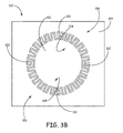
- Figure 3B is a top view of another example of the interposer of Figure 1 .
- Figure 3C is a top view of yet another example of the interposer of Figure 1 .
- Figures 4A and 4B are views of a portion of the interposer of Figure 3A illustrating, among other things, a plurality of projections for squeeze film damping.
- Figure 5 is a block diagram of an electronic device including an IMU having a vibration isolation interposer die.
- the embodiments described below relate to a vibration isolation interposer die that can be mounted between a sensor chip and a circuit board.
- the interposer die can include a base portion for mounting to a circuit board and a chip mounting portion for mounting a chip thereto.
- the interposer die can also include one or more flexures connecting the base portion to the chip mounting portion and allowing relative motion there between.
- the interposer die can also provide squeeze film dampening of the relative motion between the base portion and the chip mounting portion.
- FIG 1 is a perspective view of one example of a system 100 including a vibration isolation interposer die 102.
- the vibration isolation interposer die 102 (also referred to herein as “interposer die” or simply “interposer”) can be configured to be mounted between a chip 104 (e.g., a sensor chip) and a substrate 106 (e.g., a circuit board), and can function as the physical connection of the chip 104 to the substrate 106.
- the chip 104 can be attached to the interposer 102 which can be attached to the substrate 106.
- the interposer 102 can be attached to the substrate 106 and the chip 104 using any suitable die attach including solder, anodic bond , or other material.
- electrical connections between the substrate 106 and the chip 104 can be routed through the interposer 102.
- the interposer 102 can include suitable traces, through substrate vias, edge interconnects, or other interconnects as well as electrically conductive pads and the like to enable electrical connection to and between the chip 104 and the substrate 106.
- the interposer 102 can be composed of any suitable material, including silicon, glass, or other substrates.
- Figure 2 is a cross-sectional view of one example of the interposer 102 and the chip 104 of Figure 1 together which can comprise an inertial measurement unit (IMU).
- the chip 104 can comprise a sensor chip that includes at least three micro-electromechanical system (MEMS) gyroscopes and at least three MEMS accelerometers, each gyroscope and accelerometer oriented to sense about one of three perpendicular axes (e.g., X, Y, and Z axis).
- MEMS micro-electromechanical system
- the interposer 102 can also include a base portion 204 configured to be mounted to the substrate 106.
- Figures 3A-3C are top views of examples of the interposer 102 of Figure 1 .
- the interposer 102 can include a base portion 204 and a chip mounting portion 202.
- the interposer 102 can also include one or more flexures 302 (e.g., spring members) connecting the chip mounting portion 202 to the base portion 204.
- the one or more flexures 302 can include an elongated folded member connected to the base portion 204 and the chip mounting portion 202. Moreover, the structure (e.g., the folded structure) of the one or more flexures 302 can enable the chip mounting portion 202 to move relative to the base portion 204. This movement can enable the interposer 102 to absorb stress caused by, for example, differences in coefficients of thermal expansion between the substrate 106 and the chip 104. Additionally, the flexures 302 can be designed such that frequencies in the substrate 106 above a desired frequency are substantially absorbed and are not passed on to the chip 104.
- the interposer 102 can have a low roll-off frequency such that frequencies below approximately 100 Hz are passed to the chip 104 and frequencies above 100 Hz are absorbed by the interposer 102.
- the interposer 102 can be designed to absorb such vibration along three orthogonal axes including rotational vibration about the three orthogonal axes. Accordingly, the interposer 102 can function as a vibration isolator for the chip 104.
- the interposer 102 can include a plurality of projections 304, 306 (e.g., fins) extending out from both the chip mounting portion 202 and the base portion 204.
- a first plurality of projections 304 can comprise a plurality of generally planar structures, such as a fin, that are disposed such that they have faces that oppose one another.
- the opposing faces can be near to one another and oriented such that relative movement between the chip mounting portion 202 and the base portion 204 causes opposing faces to move toward and away from one another. This movement of the opposing faces toward and away from one another can cause squeeze film damping as the two faces cause a fluid (e.g., a gas) to be pushed out and pulled into the gap between the two faces.
- a fluid e.g., a gas
- Figures 4A and 4B are views of a portion of the interposer 102 of Figure 3A illustrating, among other things, the plurality of projections 304, 306.
- the plurality of projections include a first plurality of projections 402-1, 402-2 extending from the base portion 204 toward the chip mounting portion 202 and a second plurality of projections 404-1, 404-2 extending from the chip mounting portion 202 to the base portion 204.
- each of the first and second plurality of projections 402-1, 402-2, 404-1, 404-2 comprises a generally planar fin.
- the generally planar fins extend out perpendicularly from the base portion 204 or chip mounting portion 202 respectively.
- the projections 402-1, 402-2 from one side extend into the interstices between the projections 404-1, 404-2 extending in the opposite direction. That is, the projections 402-1, 402-2 extending from the base portion 204 extend between the projections extending from the chip mounting portion 202 and the projections 404-1, 404-2 extending from the chip mounting portion 202 extend between the projections extending from the base portion 204. Accordingly, faces of the projections 402-1 oppose faces of the projections 404-1. Thus, when the projections 402-1 move towards and away from the projections 404-1, the fluid between the projections 402-1, 404-1 is pushed out and pulled into the gap between the projections.
- the interposer 102 includes multiple subsets of the projections, wherein the multiple subsets are oriented in different directions to provide damping in different directions. For example, a first subset of projections 402-1 can be oriented in a first direction and a second subset of projections 402-2 can be oriented in a second direction orthogonal to the first direction.
- the first subset of projections 402-1 extending from the base portion 204 has a corresponding third subset 404-1 extending from the chip mounting portion 202
- the second subset of projections 402-2 extending from the base portion 204 has a corresponding fourth subset of projections 404-2 extending from the chip mounting portion 202.
- the first subset 402-1 and the third subset 404-1 can provide damping in a first direction
- a second subset 402-2 and the fourth subset 404-2 can provide damping in a second direction orthogonal to the first direction.
- the interposer 102 can include projections 304, 306 oriented in different directions.
- the projections 304, 306 are disposed in a rectangular (e.g., square) pattern.
- a first plurality of projections 304 extend from the chip mounting portion 202 and a second plurality of projections 306 extend from the base portion 204.
- the first plurality of projections 304 includes a first subset extending in a first direction, a second subset extending in a second direction, a third subset extending in a third direction, and a fourth subset extending in a fourth direction, wherein the second direction is orthogonal to the first direction, the third direction extends opposite of the first direction, and the fourth direction extends opposite of the second direction. Additionally, the first, second, third, and fourth directions are within a plane formed by the interposer 102, that is, the planar surfaces of the first, second, third, and fourth subsets are oriented generally orthogonal to the plane formed by the interposer 102.
- the second plurality of projections 306 includes a fifth subset extending into the interstices of the first subset, a sixth subset extending into the interstices of the second subset, a seventh subset extending into the interstices of the third subset, and an eighth subset extending into the interstices of the fourth subset. Accordingly, the fifth subset extends in the third direction, the sixth subset extends in the fourth direction, the seventh subset extends in the first direction, and the eighth subset extends in the second direction.
- the interposer 102 can provide squeeze film damping in two orthogonal directions within the plane formed by the interposer 102.
- Figure 3B illustrates another example where the projections 304, 306 are disposed in a circular pattern. Accordingly, a first plurality of projections 304 extend outward radially from the chip mounting portion 202. A second plurality of projections 306 extend inward radially from the base portion 204. As shown, the second plurality of projections 306 extend into the interstices of the first plurality of projections 304.
- Four flexures 302 are shown flexibly connecting the base portion 204 to the chip mounting portion 202; however other numbers and/or orientations of flexures can be used. Accordingly, rotation of the chip mounting portion 202 with respect to the base portion 204 as well as lateral movement along the plane of the interposer 202 in most directions can be damped by the projections 304, 306.
- Figure 3C illustrates yet another example where the projections 304, 306 are disposed in a circular pattern and are oriented to damp movement radially outward and inward from the chip mounting portion 202.
- a first plurality of projections 304 extend from the chip mounting portion 202 and have faces that oppose corresponding faces on a second plurality of projections 306 extending from the base portion 204. The faces are oriented to damp movement radially outward and inward with respect to the chip mounting portion.
- Four flexures 302 are shown flexibly connecting the base portion 204 to the chip mounting portion 202; however other numbers and/or orientations of flexures can be used.
- projections 304, 306 Specific examples of the pattern, orientation, number, and geometry of projections 304, 306 are provided in Figures 3A-3C . It should be understood, however, that other patterns, orientations, numbers, and geometries of projections 304, 306 can be used.
- the projections 304, 306 are disposed such that opposing faces are 10 microns or less apart from one another. In another example, the projections 304, 306 are disposed such that opposing faces are 5 microns or less apart. These distances can be used to achieve the desired squeeze film damping.
- a gap 206 formed between the interposer 102 and the chip 104 can enable squeeze film damping in the direction orthogonal to the plane formed by the interposer 102. That is, movement of the base portion 204 (e.g., up and down as shown in Figure 2 ) with respect to a chip mounting portion 202 can cause the fluid (e.g., air) within the gap 206 to be pushed out and pulled into the gap 206. This fluid movement can function to squeeze film damp movement in the direction orthogonal to the plane formed by the interposer 102 (e.g., the z-axis).
- the gap 206 between the interposer 102 and the sensor chip 104 is 10 microns or less. In another example, the gap 206 between the interposer 102 and the sensor chip 104 is 5 microns or less.
- the base portion 204 comprises the perimeter of the interposer 102 and the chip mounting portion 202 comprises an interior area of the interposer 102.
- the projections 304, 306 are disposed between the chip mounting portion 202 and the base portion 204.
- the one or more apertures (e.g., gaps) formed between the projections 304, 306 is exposed to air (e.g., exposed to the environment surrounding the interposer 102.
- air is used for squeeze film damping between the projections 304, 306, since air changes relatively slowly with temperature (compared to liquids or elastomers) the damping can be relatively constant over temperature.
- a chip mounting portion can comprise the perimeter of the interposer and the base portion can comprise the interior area of the interposer. That is, in some examples the chip 104 can be mounted to the perimeter of interposer and the interposer can be mounted to a substrate 106 in an interior area thereof. In other examples, other configurations for the chip mounting portion and the base portion can be used.
- the flexures 302 include a polymer to dampen resonance of the flexures 302.
- the projections 304, 306 can dampen movement (e.g., vibration) between the chip mounting portion 202 and the base portion 204.
- the interposer 102 can be fabricated using semiconductor processes.
- the interposer 102 can be formed by starting with a blank wafer having a plurality of future interpose dies thereon. Each of the interposer dies can be etched to form the apertures (e.g., gaps) between the base portion 204 and the chip mounting portion 202. The etching can also define the projections 304, 306 and the flexures 302. The wafer can then be singulated to form the individual interposer dies.
- An interposer die 102 can then be attached (e.g., bonded) to another chip 104 (e.g., a sensor chip) and/or a substrate 106 (e.g., a circuit board).
- the interposer 102 can include electrical interconnects therethrough to electrically couple the chip 104 to the substrate 106.
- the electrical interconnects can include one or more traces 406 on one or more of the flexures 302.
- the traces 406 on the flexures can couple a connection 408 (e.g., a die pad) on the chip mounting portion 202 with a through substrate via (TSV) 410 on the base portion 204.
- TSV through substrate via
- the die pad 408 can be configured to couple to the chip 104 and the TSV 410 can be configured to couple to the substrate 106 on a bottom side of the interposer 102.
- the trace 406 can be configured such that it will withstand the movement associated with the flexure 302. Accordingly, the chip 104 can be electrically coupled to the substrate 106 through electrical interconnects on the interposer 102. In other examples, other electrical interconnects can be used including vertical interconnects on an edge of the interposer 102.
- FIG. 5 is a block diagram of an electronic device 700 including an IMU 706 having a vibration isolation interposer die.
- the system 700 can include one or more processing devices 702 coupled to one or more memory devices 704.
- the one or more memory devices can include instruction which, when executed by the one or more processing devices 702 cause the processing devices 702 to implement navigation functions such as providing a hybrid or inertial navigation solution.
- the one or more processing devices 702 can also be coupled to an IMU 706 such as IMU 104 which can include an interposer die such as interposer die 102. Accordingly, sensors in the IMU 706 can be isolated from vibration and thermal shifting from a substrate (e.g., circuit board 106).
- the electronic device 700 can also include an input and/or output port 708 for sending and receiving signals with other devices.
- the electronic device 700 can also include other sensors such as a satellite navigation system receiver.
- the electronic device 700 can be configured to be integrated into another larger apparatus such as an aircraft, vehicle, mobile phone, or other apparatus for which inertial data is desired.
- the one or more processing devices 702 can include a central processing unit (CPU), microcontroller, microprocessor (e.g., a digital signal processor (DSP)), field programmable gate array (FPGA), application specific integrated circuit (ASIC) and other processing devices.
- the one or more processing devices 702 and the electronic device 700 can be "configured" to perform certain acts when the one or more memory devices 704 include instructions which, when executed by the one or more processing devices 702, cause the one or more processing devices 702 to perform those acts. These instructions can, for example, implement the functions of a navigation system.
- These instructions can be stored on any appropriate processor-readable medium used for storage of processor-readable instructions and/or data structures.
- This processor-readable medium can include the one or more memory devices 704 and/or other suitable media.
- Suitable processor readable media can include tangible media such as magnetic or optical media.
Abstract


Description
- This application claims the benefit of priority to
U.S. Provisional Application No. 61/416,485, filed on November 23, 2010 - Sensing systems that are used in harsh environments usually need some form of isolation from that environment. For example, an inertial measurement unit (IMU) is often subjected to vibration and/or large shocks. Therefore, a vibration isolation system is typically used to damp out the vibration and/or large shocks from the IMU.
- Conventional micro-electro-mechanical system (MEMS) IMUs can include a vibration isolator that separates the IMU housing from the internal components. This vibration isolator is typically an elastomeric material that can both absorb and damp a significant amount of vibration (e.g., approximately critically damped) over a wide temperature range (-55 degrees C to 85 degrees C).
- In an example, an interposer chip is provided. The interposer chip includes a base portion and a chip mounting portion. The interposer chip also includes one or more flexures connecting the base portion to the chip mounting portion. Additionally, a first plurality of projections extends from the base portion towards the chip mounting portion, and a second plurality of projections extends from the chip mounting portion towards the base portion and extending into interstices formed by first plurality of projections.
- Understanding that the drawings depict only exemplary embodiments and are not therefore to be considered limiting in scope, the exemplary embodiments will be described with additional specificity and detail through the use of the accompanying drawings, in which:
-
Figure 1 is a perspective view of one example of a system including a vibration isolation interposer die. -
Figure 2 is a cross-sectional view of one example of the interposer die and a sensor chip ofFigure 1 together which can comprise an inertial measurement unit (IMU). -
Figure 3A is a top view of one example of the interposer ofFigure 1 . -
Figure 3B is a top view of another example of the interposer ofFigure 1 . -
Figure 3C is a top view of yet another example of the interposer ofFigure 1 . -
Figures 4A and4B are views of a portion of the interposer ofFigure 3A illustrating, among other things, a plurality of projections for squeeze film damping. -
Figure 5 is a block diagram of an electronic device including an IMU having a vibration isolation interposer die. - In accordance with common practice, the various described features are not drawn to scale but are drawn to emphasize specific features relevant to the exemplary embodiments.
- In the following detailed description, reference is made to the accompanying drawings that form a part hereof, and in which is shown by way of illustration specific illustrative embodiments. However, it is to be understood that other embodiments may be utilized and that logical, mechanical, and electrical changes may be made. Furthermore, the method presented in the drawing figures and the specification is not to be construed as limiting the order in which the individual steps may be performed. The following detailed description is, therefore, not to be taken in a limiting sense.
- The embodiments described below relate to a vibration isolation interposer die that can be mounted between a sensor chip and a circuit board. The interposer die can include a base portion for mounting to a circuit board and a chip mounting portion for mounting a chip thereto. In some examples, the interposer die can also include one or more flexures connecting the base portion to the chip mounting portion and allowing relative motion there between. The interposer die can also provide squeeze film dampening of the relative motion between the base portion and the chip mounting portion.
-
Figure 1 is a perspective view of one example of asystem 100 including a vibration isolation interposer die 102. The vibration isolation interposer die 102 (also referred to herein as "interposer die" or simply "interposer") can be configured to be mounted between a chip 104 (e.g., a sensor chip) and a substrate 106 (e.g., a circuit board), and can function as the physical connection of thechip 104 to thesubstrate 106. Thus, thechip 104 can be attached to theinterposer 102 which can be attached to thesubstrate 106. Accordingly, theinterposer 102 can be attached to thesubstrate 106 and thechip 104 using any suitable die attach including solder, anodic bond , or other material. In some examples, electrical connections between thesubstrate 106 and thechip 104 can be routed through theinterposer 102. In these examples, theinterposer 102 can include suitable traces, through substrate vias, edge interconnects, or other interconnects as well as electrically conductive pads and the like to enable electrical connection to and between thechip 104 and thesubstrate 106. Theinterposer 102 can be composed of any suitable material, including silicon, glass, or other substrates. -
Figure 2 is a cross-sectional view of one example of theinterposer 102 and thechip 104 ofFigure 1 together which can comprise an inertial measurement unit (IMU). In this example, thechip 104 can comprise a sensor chip that includes at least three micro-electromechanical system (MEMS) gyroscopes and at least three MEMS accelerometers, each gyroscope and accelerometer oriented to sense about one of three perpendicular axes (e.g., X, Y, and Z axis). Thechip 104 can be mounted to achip mounting portion 202 of theinterposer 102. Theinterposer 102 can also include abase portion 204 configured to be mounted to thesubstrate 106. -
Figures 3A-3C are top views of examples of theinterposer 102 ofFigure 1 . As mentioned above, theinterposer 102 can include abase portion 204 and achip mounting portion 202. Theinterposer 102 can also include one or more flexures 302 (e.g., spring members) connecting thechip mounting portion 202 to thebase portion 204. - The one or
more flexures 302 can include an elongated folded member connected to thebase portion 204 and thechip mounting portion 202. Moreover, the structure (e.g., the folded structure) of the one ormore flexures 302 can enable thechip mounting portion 202 to move relative to thebase portion 204. This movement can enable theinterposer 102 to absorb stress caused by, for example, differences in coefficients of thermal expansion between thesubstrate 106 and thechip 104. Additionally, theflexures 302 can be designed such that frequencies in thesubstrate 106 above a desired frequency are substantially absorbed and are not passed on to thechip 104. In an example, theinterposer 102 can have a low roll-off frequency such that frequencies below approximately 100 Hz are passed to thechip 104 and frequencies above 100 Hz are absorbed by theinterposer 102. In some examples, theinterposer 102 can be designed to absorb such vibration along three orthogonal axes including rotational vibration about the three orthogonal axes. Accordingly, theinterposer 102 can function as a vibration isolator for thechip 104. - In an example, the
interposer 102 can include a plurality ofprojections 304, 306 (e.g., fins) extending out from both thechip mounting portion 202 and thebase portion 204. For example, a first plurality ofprojections 304 can comprise a plurality of generally planar structures, such as a fin, that are disposed such that they have faces that oppose one another. Moreover, the opposing faces can be near to one another and oriented such that relative movement between thechip mounting portion 202 and thebase portion 204 causes opposing faces to move toward and away from one another. This movement of the opposing faces toward and away from one another can cause squeeze film damping as the two faces cause a fluid (e.g., a gas) to be pushed out and pulled into the gap between the two faces. -
Figures 4A and4B are views of a portion of theinterposer 102 ofFigure 3A illustrating, among other things, the plurality ofprojections base portion 204 toward thechip mounting portion 202 and a second plurality of projections 404-1, 404-2 extending from thechip mounting portion 202 to thebase portion 204. As shown inFigure 4B , each of the first and second plurality of projections 402-1, 402-2, 404-1, 404-2 comprises a generally planar fin. The generally planar fins extend out perpendicularly from thebase portion 204 orchip mounting portion 202 respectively. Moreover, the projections 402-1, 402-2 from one side extend into the interstices between the projections 404-1, 404-2 extending in the opposite direction. That is, the projections 402-1, 402-2 extending from thebase portion 204 extend between the projections extending from thechip mounting portion 202 and the projections 404-1, 404-2 extending from thechip mounting portion 202 extend between the projections extending from thebase portion 204. Accordingly, faces of the projections 402-1 oppose faces of the projections 404-1. Thus, when the projections 402-1 move towards and away from the projections 404-1, the fluid between the projections 402-1, 404-1 is pushed out and pulled into the gap between the projections. This fluid action creates squeeze film damping of the movement of the projections 402-1, 404-1. Since this squeeze film damping occurs due to movement of the projections 402-1, 404-1 in a direction towards and away from one another, the projections 402-1, 404-1 primarily provide damping in that direction, but may provide little or no damping in directions orthogonal to that direction. Accordingly, theinterposer 102 includes multiple subsets of the projections, wherein the multiple subsets are oriented in different directions to provide damping in different directions. For example, a first subset of projections 402-1 can be oriented in a first direction and a second subset of projections 402-2 can be oriented in a second direction orthogonal to the first direction. The first subset of projections 402-1 extending from thebase portion 204 has a corresponding third subset 404-1 extending from thechip mounting portion 202, and the second subset of projections 402-2 extending from thebase portion 204 has a corresponding fourth subset of projections 404-2 extending from thechip mounting portion 202. Accordingly, the first subset 402-1 and the third subset 404-1 can provide damping in a first direction and a second subset 402-2 and the fourth subset 404-2 can provide damping in a second direction orthogonal to the first direction. - Referring back to
Figures 3A-3C , theinterposer 102 can includeprojections interposer 102 ofFigure 3A , theprojections Figure 3A , a first plurality ofprojections 304 extend from thechip mounting portion 202 and a second plurality ofprojections 306 extend from thebase portion 204. The first plurality ofprojections 304 includes a first subset extending in a first direction, a second subset extending in a second direction, a third subset extending in a third direction, and a fourth subset extending in a fourth direction, wherein the second direction is orthogonal to the first direction, the third direction extends opposite of the first direction, and the fourth direction extends opposite of the second direction. Additionally, the first, second, third, and fourth directions are within a plane formed by theinterposer 102, that is, the planar surfaces of the first, second, third, and fourth subsets are oriented generally orthogonal to the plane formed by theinterposer 102. The second plurality ofprojections 306 includes a fifth subset extending into the interstices of the first subset, a sixth subset extending into the interstices of the second subset, a seventh subset extending into the interstices of the third subset, and an eighth subset extending into the interstices of the fourth subset. Accordingly, the fifth subset extends in the third direction, the sixth subset extends in the fourth direction, the seventh subset extends in the first direction, and the eighth subset extends in the second direction. Thus, theinterposer 102 can provide squeeze film damping in two orthogonal directions within the plane formed by theinterposer 102. -
Figure 3B illustrates another example where theprojections projections 304 extend outward radially from thechip mounting portion 202. A second plurality ofprojections 306 extend inward radially from thebase portion 204. As shown, the second plurality ofprojections 306 extend into the interstices of the first plurality ofprojections 304. Fourflexures 302 are shown flexibly connecting thebase portion 204 to thechip mounting portion 202; however other numbers and/or orientations of flexures can be used. Accordingly, rotation of thechip mounting portion 202 with respect to thebase portion 204 as well as lateral movement along the plane of theinterposer 202 in most directions can be damped by theprojections -
Figure 3C illustrates yet another example where theprojections chip mounting portion 202. A first plurality ofprojections 304 extend from thechip mounting portion 202 and have faces that oppose corresponding faces on a second plurality ofprojections 306 extending from thebase portion 204. The faces are oriented to damp movement radially outward and inward with respect to the chip mounting portion. Fourflexures 302 are shown flexibly connecting thebase portion 204 to thechip mounting portion 202; however other numbers and/or orientations of flexures can be used. - Specific examples of the pattern, orientation, number, and geometry of
projections Figures 3A-3C . It should be understood, however, that other patterns, orientations, numbers, and geometries ofprojections projections projections - Referring back to
Figure 2 , agap 206 formed between theinterposer 102 and thechip 104 can enable squeeze film damping in the direction orthogonal to the plane formed by theinterposer 102. That is, movement of the base portion 204 (e.g., up and down as shown inFigure 2 ) with respect to achip mounting portion 202 can cause the fluid (e.g., air) within thegap 206 to be pushed out and pulled into thegap 206. This fluid movement can function to squeeze film damp movement in the direction orthogonal to the plane formed by the interposer 102 (e.g., the z-axis). In an example, thegap 206 between theinterposer 102 and thesensor chip 104 is 10 microns or less. In another example, thegap 206 between theinterposer 102 and thesensor chip 104 is 5 microns or less. - Referring back to
Figure 3A , in an example, thebase portion 204 comprises the perimeter of theinterposer 102 and thechip mounting portion 202 comprises an interior area of theinterposer 102. Theprojections chip mounting portion 202 and thebase portion 204. In an example, the one or more apertures (e.g., gaps) formed between theprojections interposer 102. In examples where air is used for squeeze film damping between theprojections chip 104 can be mounted to the perimeter of interposer and the interposer can be mounted to asubstrate 106 in an interior area thereof. In other examples, other configurations for the chip mounting portion and the base portion can be used. - In an example, the
flexures 302 include a polymer to dampen resonance of theflexures 302. In any case, theprojections chip mounting portion 202 and thebase portion 204. - In an example, the
interposer 102 can be fabricated using semiconductor processes. For example, theinterposer 102 can be formed by starting with a blank wafer having a plurality of future interpose dies thereon. Each of the interposer dies can be etched to form the apertures (e.g., gaps) between thebase portion 204 and thechip mounting portion 202. The etching can also define theprojections flexures 302. The wafer can then be singulated to form the individual interposer dies. An interposer die 102 can then be attached (e.g., bonded) to another chip 104 (e.g., a sensor chip) and/or a substrate 106 (e.g., a circuit board). - In an example, the
interposer 102 can include electrical interconnects therethrough to electrically couple thechip 104 to thesubstrate 106. In an example, the electrical interconnects can include one ormore traces 406 on one or more of theflexures 302. Thetraces 406 on the flexures can couple a connection 408 (e.g., a die pad) on thechip mounting portion 202 with a through substrate via (TSV) 410 on thebase portion 204. Thedie pad 408 can be configured to couple to thechip 104 and theTSV 410 can be configured to couple to thesubstrate 106 on a bottom side of theinterposer 102. Thetrace 406 can be configured such that it will withstand the movement associated with theflexure 302. Accordingly, thechip 104 can be electrically coupled to thesubstrate 106 through electrical interconnects on theinterposer 102. In other examples, other electrical interconnects can be used including vertical interconnects on an edge of theinterposer 102. -
Figure 5 is a block diagram of anelectronic device 700 including anIMU 706 having a vibration isolation interposer die. Thesystem 700 can include one ormore processing devices 702 coupled to one ormore memory devices 704. The one or more memory devices can include instruction which, when executed by the one ormore processing devices 702 cause theprocessing devices 702 to implement navigation functions such as providing a hybrid or inertial navigation solution. The one ormore processing devices 702 can also be coupled to anIMU 706 such asIMU 104 which can include an interposer die such as interposer die 102. Accordingly, sensors in theIMU 706 can be isolated from vibration and thermal shifting from a substrate (e.g., circuit board 106). Theelectronic device 700 can also include an input and/oroutput port 708 for sending and receiving signals with other devices. In some examples, theelectronic device 700 can also include other sensors such as a satellite navigation system receiver. In an example, theelectronic device 700 can be configured to be integrated into another larger apparatus such as an aircraft, vehicle, mobile phone, or other apparatus for which inertial data is desired. - The one or
more processing devices 702 can include a central processing unit (CPU), microcontroller, microprocessor (e.g., a digital signal processor (DSP)), field programmable gate array (FPGA), application specific integrated circuit (ASIC) and other processing devices. The one ormore processing devices 702 and theelectronic device 700 can be "configured" to perform certain acts when the one ormore memory devices 704 include instructions which, when executed by the one ormore processing devices 702, cause the one ormore processing devices 702 to perform those acts. These instructions can, for example, implement the functions of a navigation system. These instructions can be stored on any appropriate processor-readable medium used for storage of processor-readable instructions and/or data structures. This processor-readable medium can include the one ormore memory devices 704 and/or other suitable media. Suitable processor readable media can include tangible media such as magnetic or optical media. - Although specific embodiments have been illustrated and described herein, it will be appreciated by those of ordinary skill in the art that any arrangement, which is calculated to achieve the same purpose, may be substituted for the specific embodiments shown. Therefore, it is manifestly intended that this invention be limited only by the claims and the equivalents thereof.
Claims (10)
- An interposer chip apparatus (102) comprising:a base portion (204);a chip mounting portion (202);one or more flexures (302) connecting the base portion (204) to the chip mounting portion (202);a first plurality of projections (306) extending from the base portion (204) towards the chip mounting portion (202); anda second plurality of projections (304) extending from the chip mounting portion (202) towards the base portion (202) and extending into interstices formed by first plurality of projections (306).
- The interposer chip apparatus (102) of claim 1, wherein the first and second plurality of projections (306, 304) are configured to squeeze film dampen movement of the chip mounting portion (202) with respect to the base portion (202).
- The interposer chip apparatus (102) of any of claims 1 or 2, wherein the first plurality of projections (306) include a first subset (402-1) and a second subset (402-2) of projections, the first subset (402-1) extending in a first direction and the second subset (402-2) extending in a second direction orthogonal to the first direction;
wherein the second plurality of projections (304) include a third subset (404-1) and a fourth subset (404-2) of projections, the third subset (404-1) extending into interstices formed by the first subset (402-1) and the fourth subset (404-2) extending into interstices formed by the second subset (402-2);
wherein the first plurality of projections (304) include a fifth subset and a sixth subset of projections, the fifth subset extending in a direction opposite the first direction and the sixth subset extending in a direction opposite the second direction; and
wherein the second plurality of projections include a seventh subset and an eighth subset of projections, the seventh subset extending into interstices formed by the fifth subset and the eighth subset extending into interstices formed by the sixth subset. - The interposer chip apparatus (102) of any of claims 1-3, wherein the first and second plurality of projections (306, 304) extend in a circular pattern around the interposer chip (102) between the base portion (204) and the chip mounting portion (202).
- The interposer chip apparatus (102) of any of claims 1-4, wherein the first and second plurality of projections (306, 304) include generally planar structures disposed such that faces of the first plurality of projections (306) oppose faces of the second plurality of projections (304).
- The interposer chip apparatus (102) of claim 5, wherein the generally planar structures of the first and second plurality of projections (306, 304) are orthogonal to a plane formed by the interposer chip (102).
- The interposer chip apparatus (102) of any of claims 1-6, wherein the base portion (204) comprises a perimeter of the interposer chip (102) and the chip mounting portion (202) comprises an interior area of the interposer chip (102).
- The interposer chip apparatus (102) of any of claims 1-7, wherein gaps formed between the first and second plurality of projections (306, 304) are exposed to the environment surrounding the interposer chip (102).
- An inertial measurement unit (IMU) product (706) comprising:an interposer (102) including:a base portion (204) configured to mount to a circuit board (106);a chip mounting portion (202) configured to have a chip (104) mounted thereon;one or more spring members (302) connecting the base portion (204) to the chip mounting portion (202);wherein the base portion (204) includes a first plurality of generally planar projections (306) extending towards the chip mounting portion (202); andwherein the chip mounting portion (202) includes a second plurality of generally planar projections (304) extending towards the base portion (204) and into interstices formed by first plurality of generally planar projections (306) such that the one or more apertures are defined that weave around the first and second plurality of generally planar projections (306, 304); anda sensor chip (104) mounted to the chip mounting portion (202) of the interposer (102), the sensor chip (104) including:at least three micro-electro-mechanical system (MEMS) gyroscopes; andat least three MEMS accelerometers.
- The IMU product (706) of claim 9, wherein the first and second plurality of generally planar projections (306, 304) are disposed such that faces of the first plurality of generally planar projections (306) oppose faces of the second plurality of generally planar projections (304); and
wherein the first and second plurality of generally planar projections (306, 304) are configured to squeeze film dampen movement of the chip mounting portion (202) with respect to the base portion (204) in directions parallel to a plane of the interposer (102); and wherein a gap formed between the interposer (102) and the sensor chip (102) is configured to squeeze film dampen movement of the base portion (204) with respect the sensor chip (104) in a direction orthogonal to the plane of the interposer (102).
Applications Claiming Priority (2)
| Application Number | Priority Date | Filing Date | Title |
|---|---|---|---|
| US41648510P | 2010-11-23 | 2010-11-23 | |
| US13/299,485 US9227835B2 (en) | 2010-11-23 | 2011-11-18 | Vibration isolation interposer die |
Publications (3)
| Publication Number | Publication Date |
|---|---|
| EP2455329A2 true EP2455329A2 (en) | 2012-05-23 |
| EP2455329A3 EP2455329A3 (en) | 2014-01-01 |
| EP2455329B1 EP2455329B1 (en) | 2014-09-24 |
Family
ID=44992800
Family Applications (1)
| Application Number | Title | Priority Date | Filing Date |
|---|---|---|---|
| EP11190205.2A Active EP2455329B1 (en) | 2010-11-23 | 2011-11-22 | Vibration isolation interposer die |
Country Status (4)
| Country | Link |
|---|---|
| US (1) | US9227835B2 (en) |
| EP (1) | EP2455329B1 (en) |
| JP (1) | JP5860270B2 (en) |
| CN (1) | CN102530827A (en) |
Cited By (7)
| Publication number | Priority date | Publication date | Assignee | Title |
|---|---|---|---|---|
| WO2015185449A1 (en) * | 2014-06-06 | 2015-12-10 | Robert Bosch Gmbh | Interposer for mounting a vertically hybrid integrated component on a component carrier |
| EP2982643A1 (en) * | 2014-08-06 | 2016-02-10 | Honeywell International Inc. | Monolithic integration of stress isolation feautures in a microelectromechanical system (mems) structure |
| WO2016036544A1 (en) * | 2014-09-02 | 2016-03-10 | Apple Inc. | Various stress free sensor packages using wafer level supporting die and air gap technique |
| US9425125B2 (en) | 2014-02-20 | 2016-08-23 | Altera Corporation | Silicon-glass hybrid interposer circuitry |
| EP3217181A1 (en) * | 2016-03-11 | 2017-09-13 | Commissariat à l'énergie atomique et aux énergies alternatives | Damped linear accelerometer |
| EP3260821A1 (en) * | 2016-06-21 | 2017-12-27 | ams International AG | Sensor package and method of producing the sensor package |
| US10131535B2 (en) | 2015-05-22 | 2018-11-20 | Honeywell International Inc. | Monolithic fabrication of thermally isolated microelectromechanical system (MEMS) devices |
Families Citing this family (12)
| Publication number | Priority date | Publication date | Assignee | Title |
|---|---|---|---|---|
| US8896074B2 (en) * | 2012-01-26 | 2014-11-25 | The Charles Stark Draper Laboratory, Inc. | MEMS vibration isolation system and method |
| US20130264755A1 (en) * | 2012-04-05 | 2013-10-10 | Honeywell International Inc. | Methods and systems for limiting sensor motion |
| DE102013222966A1 (en) * | 2013-11-12 | 2015-05-28 | Robert Bosch Gmbh | inertial sensor |
| US10167189B2 (en) | 2014-09-30 | 2019-01-01 | Analog Devices, Inc. | Stress isolation platform for MEMS devices |
| US10211757B2 (en) | 2015-08-04 | 2019-02-19 | Mems Drive, Inc. | Multi-directional actuator |
| US10611628B2 (en) | 2016-12-29 | 2020-04-07 | Epack, Inc. | MEMS isolation platform with three-dimensional vibration and stress isolation |
| GB2560192A (en) * | 2017-03-03 | 2018-09-05 | Atlantic Inertial Systems Ltd | Vibration damping mount |
| US20190169018A1 (en) * | 2017-12-05 | 2019-06-06 | Invensense, Inc. | Stress isolation frame for a sensor |
| US20190241428A1 (en) * | 2018-02-06 | 2019-08-08 | Epack, Inc. | Space-efficient planar interposer for environment-resistant packaging |
| CN108609576B (en) * | 2018-04-09 | 2019-12-31 | 合肥工业大学 | Double-layer vibration isolation structure for vibration isolation of MEMS device and preparation method |
| GB2575694A (en) * | 2018-07-20 | 2020-01-22 | Atlantic Inertial Systems Ltd | Sensor packages |
| US11417611B2 (en) | 2020-02-25 | 2022-08-16 | Analog Devices International Unlimited Company | Devices and methods for reducing stress on circuit components |
Family Cites Families (22)
| Publication number | Priority date | Publication date | Assignee | Title |
|---|---|---|---|---|
| US4129042A (en) | 1977-11-18 | 1978-12-12 | Signetics Corporation | Semiconductor transducer packaged assembly |
| US4558397A (en) * | 1983-12-19 | 1985-12-10 | Amp Incorporated | Interposer connector for surface mounting a ceramic chip carrier to a printed circuit board |
| GB9009753D0 (en) * | 1990-05-01 | 1990-06-20 | Bt & D Technologies Ltd | Photo detectors |
| US5138430A (en) * | 1991-06-06 | 1992-08-11 | International Business Machines Corporation | High performance versatile thermally enhanced IC chip mounting |
| WO2001098793A2 (en) * | 2000-06-20 | 2001-12-27 | Nanonexus, Inc. | Systems for testing integraged circuits during burn-in |
| DE10010975B4 (en) * | 2000-03-07 | 2010-04-08 | Robert Bosch Gmbh | Micromechanical component |
| US6330102B1 (en) * | 2000-03-24 | 2001-12-11 | Onix Microsystems | Apparatus and method for 2-dimensional steered-beam NxM optical switch using single-axis mirror arrays and relay optics |
| JP2002071353A (en) | 2000-09-01 | 2002-03-08 | Ngk Insulators Ltd | Angular velocity measuring instrument |
| JP2002195834A (en) * | 2000-12-27 | 2002-07-10 | Murata Mfg Co Ltd | Physical quantity detector |
| US6754584B2 (en) * | 2001-02-28 | 2004-06-22 | Enpoint, Llc | Attitude measurement using a single GPS receiver with two closely-spaced antennas |
| US6937479B2 (en) | 2001-08-21 | 2005-08-30 | The Charles Stark Draper Laboratory, Inc. | Sensor isolation system |
| JP4724488B2 (en) * | 2005-02-25 | 2011-07-13 | 日立オートモティブシステムズ株式会社 | Integrated microelectromechanical system |
| US7562573B2 (en) * | 2005-07-21 | 2009-07-21 | Evigia Systems, Inc. | Integrated sensor and circuitry and process therefor |
| DE102006022807A1 (en) | 2006-05-16 | 2007-11-22 | Robert Bosch Gmbh | Chip housing with reduced vibration coupling |
| CN101796374A (en) * | 2007-09-03 | 2010-08-04 | 松下电器产业株式会社 | Inertia force sensor |
| DE102007052367A1 (en) * | 2007-11-02 | 2009-05-07 | Robert Bosch Gmbh | Micromechanical system |
| CN101271124B (en) * | 2008-05-16 | 2010-09-29 | 中国科学院上海微系统与信息技术研究所 | L-beam piezoresistance type micro-accelerometer and production method thereof |
| DE102009000574B4 (en) | 2009-02-03 | 2017-07-27 | Robert Bosch Gmbh | sensor device |
| JP2010223952A (en) | 2009-02-24 | 2010-10-07 | Seiko Epson Corp | Acceleration sensor and electronic apparatus |
| CN101792108B (en) * | 2010-03-16 | 2011-12-21 | 杭州电子科技大学 | Large capacitance micro inertial sensor based on slide-film damping and manufacturing method thereof |
| US8941222B2 (en) * | 2010-11-11 | 2015-01-27 | Advanced Semiconductor Engineering Inc. | Wafer level semiconductor package and manufacturing methods thereof |
| US8896074B2 (en) * | 2012-01-26 | 2014-11-25 | The Charles Stark Draper Laboratory, Inc. | MEMS vibration isolation system and method |
-
2011
- 2011-11-18 US US13/299,485 patent/US9227835B2/en active Active
- 2011-11-22 EP EP11190205.2A patent/EP2455329B1/en active Active
- 2011-11-22 JP JP2011255390A patent/JP5860270B2/en not_active Expired - Fee Related
- 2011-11-23 CN CN2011104568373A patent/CN102530827A/en active Pending
Non-Patent Citations (1)
| Title |
|---|
| None |
Cited By (13)
| Publication number | Priority date | Publication date | Assignee | Title |
|---|---|---|---|---|
| US9425125B2 (en) | 2014-02-20 | 2016-08-23 | Altera Corporation | Silicon-glass hybrid interposer circuitry |
| WO2015185449A1 (en) * | 2014-06-06 | 2015-12-10 | Robert Bosch Gmbh | Interposer for mounting a vertically hybrid integrated component on a component carrier |
| EP2982643A1 (en) * | 2014-08-06 | 2016-02-10 | Honeywell International Inc. | Monolithic integration of stress isolation feautures in a microelectromechanical system (mems) structure |
| US10041847B2 (en) | 2014-09-02 | 2018-08-07 | Apple Inc. | Various stress free sensor packages using wafer level supporting die and air gap technique |
| US9574959B2 (en) | 2014-09-02 | 2017-02-21 | Apple Inc. | Various stress free sensor packages using wafer level supporting die and air gap technique |
| WO2016036544A1 (en) * | 2014-09-02 | 2016-03-10 | Apple Inc. | Various stress free sensor packages using wafer level supporting die and air gap technique |
| US10131535B2 (en) | 2015-05-22 | 2018-11-20 | Honeywell International Inc. | Monolithic fabrication of thermally isolated microelectromechanical system (MEMS) devices |
| EP3217181A1 (en) * | 2016-03-11 | 2017-09-13 | Commissariat à l'énergie atomique et aux énergies alternatives | Damped linear accelerometer |
| FR3048781A1 (en) * | 2016-03-11 | 2017-09-15 | Commissariat Energie Atomique | LINEAR ACCELEROMETER AMORTI |
| US10371711B2 (en) | 2016-03-11 | 2019-08-06 | Commissariat A L'energie Atomique Et Aux Energies Alternatives | Damped linear accerelometer |
| EP3260821A1 (en) * | 2016-06-21 | 2017-12-27 | ams International AG | Sensor package and method of producing the sensor package |
| WO2017220417A1 (en) * | 2016-06-21 | 2017-12-28 | Ams International Ag | Sensor package and method of producing the sensor package |
| US11001495B2 (en) | 2016-06-21 | 2021-05-11 | Sciosense B.V. | Sensor package and method of producing the sensor package |
Also Published As
| Publication number | Publication date |
|---|---|
| JP5860270B2 (en) | 2016-02-16 |
| US20120130671A1 (en) | 2012-05-24 |
| JP2012146958A (en) | 2012-08-02 |
| EP2455329A3 (en) | 2014-01-01 |
| CN102530827A (en) | 2012-07-04 |
| EP2455329B1 (en) | 2014-09-24 |
| US9227835B2 (en) | 2016-01-05 |
Similar Documents
| Publication | Publication Date | Title |
|---|---|---|
| EP2455329B1 (en) | Vibration isolation interposer die | |
| US10611628B2 (en) | MEMS isolation platform with three-dimensional vibration and stress isolation | |
| US8896074B2 (en) | MEMS vibration isolation system and method | |
| JP2018146569A (en) | Vibration damping mount | |
| KR20070046001A (en) | Mems sensor systems and methods | |
| EP3403992A1 (en) | Systems and methods for multi-sensor integrated sensor devices | |
| EP2840375A1 (en) | Device with a micro- or nanoscale structure | |
| US11650221B2 (en) | MEMS tri-axial accelerometer with one or more decoupling elements | |
| US20160229689A1 (en) | Packaged Microchip with Patterned Interposer | |
| US9625284B2 (en) | Shock mount in environment sensor protector for non-isolated systems | |
| US20170107098A1 (en) | Microelectromechanical system and fabricating process | |
| US20210061291A1 (en) | Inertial Sensor Unit, Electronic Apparatus, And Vehicle | |
| US10988375B1 (en) | Systems, methods, and devices for mechanical isolation or mechanical damping of microfabricated inertial sensors | |
| CN108572042A (en) | Pressure sensor and its manufacturing method, pressure sensor module, electronic equipment and moving body | |
| KR101482400B1 (en) | Micro Electro Mechanical Systems Component | |
| US9963339B2 (en) | Sensor device | |
| JP2020071069A (en) | Physical quantity sensor, electronic apparatus, and moving body | |
| US11282808B2 (en) | Inertial sensor, electronic instrument, vehicle, and method for manufacturing inertial sensor | |
| CN113148942A (en) | External packaging structure, MEMS sensor and electronic equipment | |
| CN111811504A (en) | Laminated micro-inertia measuring unit under large-overload high-dynamic application environment | |
| JP2021022680A (en) | Wiring board, electronic device, and electronic module | |
| CN212482500U (en) | Laminated micro-inertia measuring unit under large-overload high-dynamic application environment | |
| KR101496949B1 (en) | Inertial sensor having vibration proof function and fabrication method thereof | |
| WO2021220574A1 (en) | Sensor module | |
| JP2018165651A (en) | Sensor device, electronic device and moving body |
Legal Events
| Date | Code | Title | Description |
|---|---|---|---|
| PUAI | Public reference made under article 153(3) epc to a published international application that has entered the european phase |
Free format text: ORIGINAL CODE: 0009012 |
|
| 17P | Request for examination filed |
Effective date: 20111122 |
|
| AK | Designated contracting states |
Kind code of ref document: A2 Designated state(s): AL AT BE BG CH CY CZ DE DK EE ES FI FR GB GR HR HU IE IS IT LI LT LU LV MC MK MT NL NO PL PT RO RS SE SI SK SM TR |
|
| AX | Request for extension of the european patent |
Extension state: BA ME |
|
| REG | Reference to a national code |
Ref country code: DE Ref legal event code: R079 Ref document number: 602011010075 Country of ref document: DE Free format text: PREVIOUS MAIN CLASS: B81B0007000000 Ipc: H01L0021768000 |
|
| PUAL | Search report despatched |
Free format text: ORIGINAL CODE: 0009013 |
|
| AK | Designated contracting states |
Kind code of ref document: A3 Designated state(s): AL AT BE BG CH CY CZ DE DK EE ES FI FR GB GR HR HU IE IS IT LI LT LU LV MC MK MT NL NO PL PT RO RS SE SI SK SM TR |
|
| AX | Request for extension of the european patent |
Extension state: BA ME |
|
| RIC1 | Information provided on ipc code assigned before grant |
Ipc: H01L 21/768 20060101AFI20131128BHEP Ipc: H01L 25/065 20060101ALI20131128BHEP |
|
| 17Q | First examination report despatched |
Effective date: 20131212 |
|
| GRAP | Despatch of communication of intention to grant a patent |
Free format text: ORIGINAL CODE: EPIDOSNIGR1 |
|
| INTG | Intention to grant announced |
Effective date: 20140612 |
|
| GRAS | Grant fee paid |
Free format text: ORIGINAL CODE: EPIDOSNIGR3 |
|
| GRAA | (expected) grant |
Free format text: ORIGINAL CODE: 0009210 |
|
| AK | Designated contracting states |
Kind code of ref document: B1 Designated state(s): AL AT BE BG CH CY CZ DE DK EE ES FI FR GB GR HR HU IE IS IT LI LT LU LV MC MK MT NL NO PL PT RO RS SE SI SK SM TR |
|
| REG | Reference to a national code |
Ref country code: GB Ref legal event code: FG4D |
|
| REG | Reference to a national code |
Ref country code: CH Ref legal event code: EP |
|
| REG | Reference to a national code |
Ref country code: AT Ref legal event code: REF Ref document number: 688946 Country of ref document: AT Kind code of ref document: T Effective date: 20141015 |
|
| REG | Reference to a national code |
Ref country code: IE Ref legal event code: FG4D |
|
| REG | Reference to a national code |
Ref country code: DE Ref legal event code: R096 Ref document number: 602011010075 Country of ref document: DE Effective date: 20141106 |
|
| PG25 | Lapsed in a contracting state [announced via postgrant information from national office to epo] |
Ref country code: SE Free format text: LAPSE BECAUSE OF FAILURE TO SUBMIT A TRANSLATION OF THE DESCRIPTION OR TO PAY THE FEE WITHIN THE PRESCRIBED TIME-LIMIT Effective date: 20140924 Ref country code: GR Free format text: LAPSE BECAUSE OF FAILURE TO SUBMIT A TRANSLATION OF THE DESCRIPTION OR TO PAY THE FEE WITHIN THE PRESCRIBED TIME-LIMIT Effective date: 20141225 Ref country code: LT Free format text: LAPSE BECAUSE OF FAILURE TO SUBMIT A TRANSLATION OF THE DESCRIPTION OR TO PAY THE FEE WITHIN THE PRESCRIBED TIME-LIMIT Effective date: 20140924 Ref country code: FI Free format text: LAPSE BECAUSE OF FAILURE TO SUBMIT A TRANSLATION OF THE DESCRIPTION OR TO PAY THE FEE WITHIN THE PRESCRIBED TIME-LIMIT Effective date: 20140924 Ref country code: NO Free format text: LAPSE BECAUSE OF FAILURE TO SUBMIT A TRANSLATION OF THE DESCRIPTION OR TO PAY THE FEE WITHIN THE PRESCRIBED TIME-LIMIT Effective date: 20141224 |
|
| REG | Reference to a national code |
Ref country code: LT Ref legal event code: MG4D Ref country code: NL Ref legal event code: VDEP Effective date: 20140924 |
|
| PG25 | Lapsed in a contracting state [announced via postgrant information from national office to epo] |
Ref country code: RS Free format text: LAPSE BECAUSE OF FAILURE TO SUBMIT A TRANSLATION OF THE DESCRIPTION OR TO PAY THE FEE WITHIN THE PRESCRIBED TIME-LIMIT Effective date: 20140924 Ref country code: CY Free format text: LAPSE BECAUSE OF FAILURE TO SUBMIT A TRANSLATION OF THE DESCRIPTION OR TO PAY THE FEE WITHIN THE PRESCRIBED TIME-LIMIT Effective date: 20140924 Ref country code: LV Free format text: LAPSE BECAUSE OF FAILURE TO SUBMIT A TRANSLATION OF THE DESCRIPTION OR TO PAY THE FEE WITHIN THE PRESCRIBED TIME-LIMIT Effective date: 20140924 Ref country code: HR Free format text: LAPSE BECAUSE OF FAILURE TO SUBMIT A TRANSLATION OF THE DESCRIPTION OR TO PAY THE FEE WITHIN THE PRESCRIBED TIME-LIMIT Effective date: 20140924 |
|
| REG | Reference to a national code |
Ref country code: AT Ref legal event code: MK05 Ref document number: 688946 Country of ref document: AT Kind code of ref document: T Effective date: 20140924 |
|
| PG25 | Lapsed in a contracting state [announced via postgrant information from national office to epo] |
Ref country code: NL Free format text: LAPSE BECAUSE OF FAILURE TO SUBMIT A TRANSLATION OF THE DESCRIPTION OR TO PAY THE FEE WITHIN THE PRESCRIBED TIME-LIMIT Effective date: 20140924 |
|
| PG25 | Lapsed in a contracting state [announced via postgrant information from national office to epo] |
Ref country code: IS Free format text: LAPSE BECAUSE OF FAILURE TO SUBMIT A TRANSLATION OF THE DESCRIPTION OR TO PAY THE FEE WITHIN THE PRESCRIBED TIME-LIMIT Effective date: 20150124 Ref country code: EE Free format text: LAPSE BECAUSE OF FAILURE TO SUBMIT A TRANSLATION OF THE DESCRIPTION OR TO PAY THE FEE WITHIN THE PRESCRIBED TIME-LIMIT Effective date: 20140924 Ref country code: ES Free format text: LAPSE BECAUSE OF FAILURE TO SUBMIT A TRANSLATION OF THE DESCRIPTION OR TO PAY THE FEE WITHIN THE PRESCRIBED TIME-LIMIT Effective date: 20140924 Ref country code: PT Free format text: LAPSE BECAUSE OF FAILURE TO SUBMIT A TRANSLATION OF THE DESCRIPTION OR TO PAY THE FEE WITHIN THE PRESCRIBED TIME-LIMIT Effective date: 20150126 Ref country code: CZ Free format text: LAPSE BECAUSE OF FAILURE TO SUBMIT A TRANSLATION OF THE DESCRIPTION OR TO PAY THE FEE WITHIN THE PRESCRIBED TIME-LIMIT Effective date: 20140924 Ref country code: SK Free format text: LAPSE BECAUSE OF FAILURE TO SUBMIT A TRANSLATION OF THE DESCRIPTION OR TO PAY THE FEE WITHIN THE PRESCRIBED TIME-LIMIT Effective date: 20140924 Ref country code: RO Free format text: LAPSE BECAUSE OF FAILURE TO SUBMIT A TRANSLATION OF THE DESCRIPTION OR TO PAY THE FEE WITHIN THE PRESCRIBED TIME-LIMIT Effective date: 20140924 |
|
| PG25 | Lapsed in a contracting state [announced via postgrant information from national office to epo] |
Ref country code: AT Free format text: LAPSE BECAUSE OF FAILURE TO SUBMIT A TRANSLATION OF THE DESCRIPTION OR TO PAY THE FEE WITHIN THE PRESCRIBED TIME-LIMIT Effective date: 20140924 Ref country code: PL Free format text: LAPSE BECAUSE OF FAILURE TO SUBMIT A TRANSLATION OF THE DESCRIPTION OR TO PAY THE FEE WITHIN THE PRESCRIBED TIME-LIMIT Effective date: 20140924 |
|
| REG | Reference to a national code |
Ref country code: DE Ref legal event code: R097 Ref document number: 602011010075 Country of ref document: DE |
|
| PG25 | Lapsed in a contracting state [announced via postgrant information from national office to epo] |
Ref country code: LU Free format text: LAPSE BECAUSE OF FAILURE TO SUBMIT A TRANSLATION OF THE DESCRIPTION OR TO PAY THE FEE WITHIN THE PRESCRIBED TIME-LIMIT Effective date: 20141122 Ref country code: MC Free format text: LAPSE BECAUSE OF FAILURE TO SUBMIT A TRANSLATION OF THE DESCRIPTION OR TO PAY THE FEE WITHIN THE PRESCRIBED TIME-LIMIT Effective date: 20140924 Ref country code: BE Free format text: LAPSE BECAUSE OF NON-PAYMENT OF DUE FEES Effective date: 20141130 |
|
| PG25 | Lapsed in a contracting state [announced via postgrant information from national office to epo] |
Ref country code: DK Free format text: LAPSE BECAUSE OF FAILURE TO SUBMIT A TRANSLATION OF THE DESCRIPTION OR TO PAY THE FEE WITHIN THE PRESCRIBED TIME-LIMIT Effective date: 20140924 |
|
| PLBE | No opposition filed within time limit |
Free format text: ORIGINAL CODE: 0009261 |
|
| STAA | Information on the status of an ep patent application or granted ep patent |
Free format text: STATUS: NO OPPOSITION FILED WITHIN TIME LIMIT |
|
| REG | Reference to a national code |
Ref country code: IE Ref legal event code: MM4A |
|
| PG25 | Lapsed in a contracting state [announced via postgrant information from national office to epo] |
Ref country code: IT Free format text: LAPSE BECAUSE OF FAILURE TO SUBMIT A TRANSLATION OF THE DESCRIPTION OR TO PAY THE FEE WITHIN THE PRESCRIBED TIME-LIMIT Effective date: 20140924 |
|
| 26N | No opposition filed |
Effective date: 20150625 |
|
| REG | Reference to a national code |
Ref country code: FR Ref legal event code: PLFP Year of fee payment: 5 |
|
| PG25 | Lapsed in a contracting state [announced via postgrant information from national office to epo] |
Ref country code: IE Free format text: LAPSE BECAUSE OF NON-PAYMENT OF DUE FEES Effective date: 20141122 |
|
| PGFP | Annual fee paid to national office [announced via postgrant information from national office to epo] |
Ref country code: DE Payment date: 20151130 Year of fee payment: 5 Ref country code: CH Payment date: 20151026 Year of fee payment: 5 |
|
| PG25 | Lapsed in a contracting state [announced via postgrant information from national office to epo] |
Ref country code: SI Free format text: LAPSE BECAUSE OF FAILURE TO SUBMIT A TRANSLATION OF THE DESCRIPTION OR TO PAY THE FEE WITHIN THE PRESCRIBED TIME-LIMIT Effective date: 20140924 |
|
| PG25 | Lapsed in a contracting state [announced via postgrant information from national office to epo] |
Ref country code: SM Free format text: LAPSE BECAUSE OF FAILURE TO SUBMIT A TRANSLATION OF THE DESCRIPTION OR TO PAY THE FEE WITHIN THE PRESCRIBED TIME-LIMIT Effective date: 20140924 |
|
| PG25 | Lapsed in a contracting state [announced via postgrant information from national office to epo] |
Ref country code: BG Free format text: LAPSE BECAUSE OF FAILURE TO SUBMIT A TRANSLATION OF THE DESCRIPTION OR TO PAY THE FEE WITHIN THE PRESCRIBED TIME-LIMIT Effective date: 20140924 |
|
| PG25 | Lapsed in a contracting state [announced via postgrant information from national office to epo] |
Ref country code: HU Free format text: LAPSE BECAUSE OF FAILURE TO SUBMIT A TRANSLATION OF THE DESCRIPTION OR TO PAY THE FEE WITHIN THE PRESCRIBED TIME-LIMIT; INVALID AB INITIO Effective date: 20111122 Ref country code: MT Free format text: LAPSE BECAUSE OF FAILURE TO SUBMIT A TRANSLATION OF THE DESCRIPTION OR TO PAY THE FEE WITHIN THE PRESCRIBED TIME-LIMIT Effective date: 20140924 Ref country code: TR Free format text: LAPSE BECAUSE OF FAILURE TO SUBMIT A TRANSLATION OF THE DESCRIPTION OR TO PAY THE FEE WITHIN THE PRESCRIBED TIME-LIMIT Effective date: 20140924 |
|
| REG | Reference to a national code |
Ref country code: FR Ref legal event code: PLFP Year of fee payment: 6 |
|
| REG | Reference to a national code |
Ref country code: DE Ref legal event code: R119 Ref document number: 602011010075 Country of ref document: DE |
|
| REG | Reference to a national code |
Ref country code: CH Ref legal event code: PL |
|
| PG25 | Lapsed in a contracting state [announced via postgrant information from national office to epo] |
Ref country code: LI Free format text: LAPSE BECAUSE OF NON-PAYMENT OF DUE FEES Effective date: 20161130 Ref country code: CH Free format text: LAPSE BECAUSE OF NON-PAYMENT OF DUE FEES Effective date: 20161130 |
|
| REG | Reference to a national code |
Ref country code: FR Ref legal event code: PLFP Year of fee payment: 7 |
|
| PG25 | Lapsed in a contracting state [announced via postgrant information from national office to epo] |
Ref country code: DE Free format text: LAPSE BECAUSE OF NON-PAYMENT OF DUE FEES Effective date: 20170601 |
|
| PG25 | Lapsed in a contracting state [announced via postgrant information from national office to epo] |
Ref country code: MK Free format text: LAPSE BECAUSE OF FAILURE TO SUBMIT A TRANSLATION OF THE DESCRIPTION OR TO PAY THE FEE WITHIN THE PRESCRIBED TIME-LIMIT Effective date: 20140924 |
|
| PG25 | Lapsed in a contracting state [announced via postgrant information from national office to epo] |
Ref country code: AL Free format text: LAPSE BECAUSE OF FAILURE TO SUBMIT A TRANSLATION OF THE DESCRIPTION OR TO PAY THE FEE WITHIN THE PRESCRIBED TIME-LIMIT Effective date: 20140924 |
|
| P01 | Opt-out of the competence of the unified patent court (upc) registered |
Effective date: 20230525 |
|
| PGFP | Annual fee paid to national office [announced via postgrant information from national office to epo] |
Ref country code: GB Payment date: 20231121 Year of fee payment: 13 |
|
| PGFP | Annual fee paid to national office [announced via postgrant information from national office to epo] |
Ref country code: FR Payment date: 20231123 Year of fee payment: 13 |