EP2454573B1 - Nems mit transduktionsvorrichtung auf der basis einer al-si-legierung - Google Patents
Nems mit transduktionsvorrichtung auf der basis einer al-si-legierung Download PDFInfo
- Publication number
- EP2454573B1 EP2454573B1 EP10731526.9A EP10731526A EP2454573B1 EP 2454573 B1 EP2454573 B1 EP 2454573B1 EP 10731526 A EP10731526 A EP 10731526A EP 2454573 B1 EP2454573 B1 EP 2454573B1
- Authority
- EP
- European Patent Office
- Prior art keywords
- movable part
- alsi
- layer
- sensor
- substrate
- Prior art date
- Legal status (The legal status is an assumption and is not a legal conclusion. Google has not performed a legal analysis and makes no representation as to the accuracy of the status listed.)
- Not-in-force
Links
Images






Classifications
-
- G—PHYSICS
- G01—MEASURING; TESTING
- G01P—MEASURING LINEAR OR ANGULAR SPEED, ACCELERATION, DECELERATION, OR SHOCK; INDICATING PRESENCE, ABSENCE, OR DIRECTION, OF MOVEMENT
- G01P15/00—Measuring acceleration; Measuring deceleration; Measuring shock, i.e. sudden change of acceleration
- G01P15/02—Measuring acceleration; Measuring deceleration; Measuring shock, i.e. sudden change of acceleration by making use of inertia forces using solid seismic masses
- G01P15/08—Measuring acceleration; Measuring deceleration; Measuring shock, i.e. sudden change of acceleration by making use of inertia forces using solid seismic masses with conversion into electric or magnetic values
- G01P15/097—Measuring acceleration; Measuring deceleration; Measuring shock, i.e. sudden change of acceleration by making use of inertia forces using solid seismic masses with conversion into electric or magnetic values by vibratory elements
-
- B—PERFORMING OPERATIONS; TRANSPORTING
- B81—MICROSTRUCTURAL TECHNOLOGY
- B81B—MICROSTRUCTURAL DEVICES OR SYSTEMS, e.g. MICROMECHANICAL DEVICES
- B81B3/00—Devices comprising flexible or deformable elements, e.g. comprising elastic tongues or membranes
- B81B3/0018—Structures acting upon the moving or flexible element for transforming energy into mechanical movement or vice versa, i.e. actuators, sensors, generators
- B81B3/0021—Transducers for transforming electrical into mechanical energy or vice versa
-
- G—PHYSICS
- G01—MEASURING; TESTING
- G01N—INVESTIGATING OR ANALYSING MATERIALS BY DETERMINING THEIR CHEMICAL OR PHYSICAL PROPERTIES
- G01N29/00—Investigating or analysing materials by the use of ultrasonic, sonic or infrasonic waves; Visualisation of the interior of objects by transmitting ultrasonic or sonic waves through the object
- G01N29/02—Analysing fluids
- G01N29/022—Fluid sensors based on microsensors, e.g. quartz crystal-microbalance [QCM], surface acoustic wave [SAW] devices, tuning forks, cantilevers, flexural plate wave [FPW] devices
-
- G—PHYSICS
- G01—MEASURING; TESTING
- G01P—MEASURING LINEAR OR ANGULAR SPEED, ACCELERATION, DECELERATION, OR SHOCK; INDICATING PRESENCE, ABSENCE, OR DIRECTION, OF MOVEMENT
- G01P15/00—Measuring acceleration; Measuring deceleration; Measuring shock, i.e. sudden change of acceleration
- G01P15/02—Measuring acceleration; Measuring deceleration; Measuring shock, i.e. sudden change of acceleration by making use of inertia forces using solid seismic masses
- G01P15/08—Measuring acceleration; Measuring deceleration; Measuring shock, i.e. sudden change of acceleration by making use of inertia forces using solid seismic masses with conversion into electric or magnetic values
- G01P15/12—Measuring acceleration; Measuring deceleration; Measuring shock, i.e. sudden change of acceleration by making use of inertia forces using solid seismic masses with conversion into electric or magnetic values by alteration of electrical resistance
- G01P15/123—Measuring acceleration; Measuring deceleration; Measuring shock, i.e. sudden change of acceleration by making use of inertia forces using solid seismic masses with conversion into electric or magnetic values by alteration of electrical resistance by piezo-resistive elements, e.g. semiconductor strain gauges
-
- B—PERFORMING OPERATIONS; TRANSPORTING
- B81—MICROSTRUCTURAL TECHNOLOGY
- B81B—MICROSTRUCTURAL DEVICES OR SYSTEMS, e.g. MICROMECHANICAL DEVICES
- B81B2203/00—Basic microelectromechanical structures
- B81B2203/01—Suspended structures, i.e. structures allowing a movement
- B81B2203/0118—Cantilevers
-
- B—PERFORMING OPERATIONS; TRANSPORTING
- B81—MICROSTRUCTURAL TECHNOLOGY
- B81B—MICROSTRUCTURAL DEVICES OR SYSTEMS, e.g. MICROMECHANICAL DEVICES
- B81B2203/00—Basic microelectromechanical structures
- B81B2203/05—Type of movement
- B81B2203/058—Rotation out of a plane parallel to the substrate
-
- G—PHYSICS
- G01—MEASURING; TESTING
- G01N—INVESTIGATING OR ANALYSING MATERIALS BY DETERMINING THEIR CHEMICAL OR PHYSICAL PROPERTIES
- G01N2291/00—Indexing codes associated with group G01N29/00
- G01N2291/01—Indexing codes associated with the measuring variable
- G01N2291/014—Resonance or resonant frequency
-
- G—PHYSICS
- G01—MEASURING; TESTING
- G01N—INVESTIGATING OR ANALYSING MATERIALS BY DETERMINING THEIR CHEMICAL OR PHYSICAL PROPERTIES
- G01N2291/00—Indexing codes associated with group G01N29/00
- G01N2291/04—Wave modes and trajectories
- G01N2291/042—Wave modes
- G01N2291/0427—Flexural waves, plate waves, e.g. Lamb waves, tuning fork, cantilever
Definitions
- the invention relates to devices known as NEMS (for "Nano Electro-Mechanical Systems") comprising at least one movable part associated with transduction means (of excitation and/or detection).
- NEMS for "Nano Electro-Mechanical Systems”
- transduction means of excitation and/or detection
- NEMS necessitates developing integrable actuation and detection principles, adapted to detecting slight deformations at high frequencies compared to the displacements and frequencies brought into play in micro-sensors, produced by MEMS (for "Micro Electro-Mechanical Systems") technologies.
- MEMS Micro Electro-Mechanical Systems
- the principles available must make it possible to design simple patterns and production methods.
- the techniques implemented must remain compatible with the tools and methods of microelectronics so that their very large scale integration, via clean rooms or microelectronic foundries, is accessible.
- the pertinence of the principles of thermoelastic actuation and piezoresistive detection has been demonstrated. Reference may be made in this respect to the article " Ultra-sensitive NEMS-based cantilevers for sensing, scanned probe and very high-frequency applications" of Mo Li et al., Nature Nanotechnology, Volume 2, N°2, pages 114 to 120, 2007 .
- thermoelastic actuation in order to limit the consumption and to guarantee the optimal efficiency of the actuator, materials with TEC (thermal expansion coefficient) as different as possible must be chosen.
- TEC thermo expansion coefficient
- the variation in resistance ⁇ R linked to the variation in strain ( ⁇ ) induced by the deformation of the material ( ⁇ R being proportional to the strain), may be known.
- the first term corresponds to the piezoresistive effect strictly speaking whereas the second corresponds to a purely geometric effect. In the case of a semi-conductor such as silicon, the second term is of several orders of magnitude less than the first.
- Piezoresistivity is a physical phenomenon that links this variation in resistivity to a strain applied to the gauge.
- ⁇ ij are the elements of the piezoresistivity tensor expressed along the main crystalline axes of the semi-conductor.
- ⁇ L , ⁇ T are respectively the longitudinal and transversal piezoresistive coefficients expressed in the principal mark of the gauge (N, T).
- ⁇ L and ⁇ T are respectively the longitudinal and transversal strains applied.
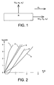
- figure 1 which is a diagram of a piezoresistive gauge and associated principal axes (N, T).
- l i , m i and n i are the coordinates of the director vectors T and N in relation to the crystalline base of the material.
- ⁇ (known as the gauge factor) is of the order of several units (see table 1 and figure 1 ).
- the equation (3) can also amount to a form equivalent to (4) using Hooke's law.
- ⁇ is between 50 and 200, depending on the type of doping and the crystalline axes considered.
- Table 1 gives some examples of gauge factor for commonly used alloys used and silicon. Table 1 Materials Gauge factor Final elongation (%) Low deformation High deformation Copper 2.6 2.2 0.5 Mangan 2.1 1.9 1.0 Nickel -12 2.7 - Platinum 6.1 2.4 0.4 Silver 2.9 2.4 0.8 40% gold/palladium 0.9 1.9 0.8 Semiconductor ⁇ 100 -600 -
- Ni is an alloy of copper and nickel Cu 6o Ni 40 , similar to the annealed alloys of copper and nickel called “Ferry”, “Advance” and “Copel”.
- the gauge factor of a semiconductor material largely depends on its level of doping and on its doping species.
- Figure 2 is a diagram illustrating, for several metallic materials, the variation in resistance in % ⁇ R/R as a function of the percentage deformation D of these materials.
- the gauge factor for a material is the slope of the corresponding curve. Curve 1 has been drawn for the alloy 10% rhodium/platinum, curve 2 for the alloy "Ferry”, curve 3 for constantan, curve 4 for the alloy 40% gold/platinum and curve 5 for nickel. It may be seen that for small deformations, the gauge factor of nickel is negative.
- Figure 3 is taken from the document " Electrical resistance-strain characteristics of thin evaporated metal films" of R. L. Parker et al., Journal of Applied Physics, Vol. 34, N°9, September 1963, pages 2700 to 2708 .
- This figure represents the gauge factor ⁇ as a function of the resistance R s of a layer of aluminium. It may be observed that the gauge factor for aluminium alone can become negative for certain resistance values (see zone A), in other words for certain geometric parameters.
- the gauge factors in intrinsic Si are much higher (several hundreds) than in the case of metal materials (between 2 and 4). Since intrinsic silicon is too resistive, it is doped in order to make it more conductive. In doing so, the gauge factor decreases but remains all the same around 100 for doping levels close to 10 19 cm -3 , in other words for doping ranges among the highest commonly used in microelectronics. At such levels, the resistivity of the material is of the order of 10 m ⁇ .cm.
- the use of metal layers as sensitive piezoresistive component becomes advantageous.
- the semi-conducting gauges at the scale of a NEMS sensor have very small typical sections (of the order of 0.2 nm 2 ).
- their resistances have high unit length values, which makes the measurement very awkward (reduction of the signal by resistive bridge effect for example). It is then necessary to highly dope the gauge beyond 10 19 cm -3 , which strongly reduces the gauge coefficient value.
- the mass resolution is proportional to the noise density of the gauge and inversely proportional to the detection gain of said gauge given to the first order by the product reading voltage, gauge factor. Given the high resistivities and lower gauge value of semi-conducting gauges, the resolution drops to values close to those obtained with metal sensitive layers.
- the ambient temperature may be low, of the order of 50 K. At these temperatures, there exists an effect known as "carrier freeze-out" in semiconductors increasing very considerably their resistivity. The use of semi-conducting gauges for this application is thus disadvantageous compared to metal layers.
- aluminium or a metallic alloy based on aluminium are proposed as potentially interesting layer. Nevertheless, those skilled in the art know that aluminium deposited without precaution on silicon migrates into the semiconductor. Thus, the invention proposes forming an alloy based on aluminium integrating silicon (in typical proportions between 1% and 2%) to avoid the problems of migration.
- the alloy AlCuSi is also used not only to avoid the eutectic but also to limit the effects of electromigration of the aluminium into the silicon and inversely when a rise in temperature induced by Joule effect in the current loop becomes significant.
- This AlSi alloy has been used for interconnection applications in microelectronics in the 1970s. Reference may be made in this respect to the document JP-A-61-239 644 .
- the materials AlSi and AlCuSi have never, on the other hand, been considered as materials suited to being used in thin film to form a piezoresistive transduction.
- the gauge factor of an aluminium alloy based material is low and its resistivity is very low. In other words, that signifies that the signal applied to a sensitive component based on aluminium alloy must be very weak to avoid any fusion of the component by fusible effect. Furthermore, the transduction is not very efficient due to its low gauge factor. Since the displacements and the strains in the movable mechanical components of the microsystems are high, all of these arguments incite those skilled in the art to rule out this type of layer to form the sensitive layer.
- Frequency detection consists in measuring any shift in the mechanical resonance frequency of an oscillating component when it is subjected to a given stimulus. In the case of the invention, it involves measuring a frequency shift when a very small mass settles on the surface of the sensitive component.
- the size of the NEMS is thus favourable to attain high sensitivities.
- the mechanical frequencies attained with these nano-structures are high (100 MHz and above). It is thus advantageous that the input impedances of the sensor and the electrical circuits are close and adapted 50 ⁇ .
- the material must also resist the techniques of etching of the sacrificial layer achieving the release making it possible to obtain the movable part (for example, etching based on HF).
- CMOS compatible materials capable of meeting the listed requirements.
- the inventors of the present invention have studied numerous possibilities of use of materials compatible with a CMOS foundry and making it possible to form both the sensitive piezoresistive layer and the thermoelastic actuation layer of NEMS sensors.
- these materials may be cited the following: PtSi, NiSi, TiSi 2 , AlSi, WSi 2 , TiN, TiN/Cu, Cu, Ti, Cr, Ni and W.
- the object of the invention is thus a Nano ElectroMechanical System (NEMS) comprising at least one fixed part associated with a substrate and at least one movable part in relation to the substrate, said system comprising transduction means capable of exciting the movable part to confer on it a movement and/or to detect a movement of the movable part, the transduction means comprising at least one electrically conductive transduction material, characterised in that the electrically conductive transduction material is formed of an AlSi alloy based deposition, said deposition being supported at least in part by the movable part of the system.
- NEMS Nano ElectroMechanical System
- the AlSi alloy based deposition may be an alloy chosen among AlSi and AlCuSi.
- the alloy of AlSi is particularly advantageous, particularly for technological implementation reasons (limited number of steps).
- the transduction means may further comprise, under the electrically conductive material, an additional layer to structure the electrically conductive material and/or to amplify the movement detected and/or to form a barrier to the diffusion of the conductive material.
- This additional layer may be a layer of Ti or Ti/TiN.
- the AlSi alloy based deposition may form at least one current loop for the excitation of the movable part and/or for the detection of a movement of the movable part. It can form two overlapping current loops, one for the excitation of the movable part and the other for the detection of a movement of the movable part.
- the movable part of the system may comprise a clamped-free beam or a clamped-clamped beam.
- a clamped-free beam or a clamped-clamped beam.
- other shapes of movable part may be used such as for example a plate, a disc, a ring, a coil, etc. and anchored by at least one anchoring point to the substrate.
- the substrate may comprise a support covered successively with an electrically insulating layer and a superficial silicon layer, said fixed and movable parts being formed in the superficial silicon layer, the movable part being obtained thanks to a hollowing out formed in the electrically insulating layer.
- the system further comprising a test mass, the movable part is attached by one of its ends to the substrate and by its other end to the test mass, the transduction means being means capable of detecting a movement.
- the system further comprising a test mass, a resonator connects the test mass to the substrate, the movable part being attached by one of its ends to the substrate and by its other end to the resonator, the transduction means being means capable of detecting an acceleration.
- the AlSi alloy based deposition may have a thickness between 10 and 100 nm, preferably between 40 and 80 nm.
- the system may further comprise at least one deposition of an electrografted functionalization layer, beyond the AlSi alloy based material.
- the NEMS according to the invention may apply to the production of a sensor chosen among a mass sensor, a gas sensor, a biochemical sensor, a force sensor, an inertial sensor and a pressure sensor.
- the AlSi alloy according to the invention comprises between 0.5 % and 4 % of silicon by weight and preferentially 1 %.
- the maximum quantity of materials, mixed with aluminium in the alloy, is determined by the limit of solubility of these materials in this alloy, as a function of the maximum temperature used in NEMS production methods.
- Figure 4 is a top view of a clamped-free beam (or cantilever beam) bearing a current loop common to thermoelastic actuation and to piezoresistive detection.
- the beam 10 is fixed to the substrate by parts 11 and 12 and is overhanging from these parts.
- the current loop is defined from the parts 11 and 12 by an interval 13.
- Table 2 gives examples of dimensions (in ⁇ m) for such a beam.
- Table 2 l w l 1 b s 1.5 0.6 0.5 0.2 0.2 2.8 0.7 1 0.25 0.2 5 1 2 0.3 0.4
- Figures 5A to 5C are longitudinal sectional views illustrating a method of producing the clamped-free beam of figure 4 .
- Figure 5A shows an SOI substrate 20 constituted of a silicon support 21 supporting successively a buried oxide layer 22 and a superficial silicon layer 23.
- An AlSi layer 24 of 50 nm thickness is formed on the superficial layer 23.
- the definition of the electrically conductive part of the beam on the superficial layer 23 is then carried out by photolithography and etching for example by chlorinated plasma such as BCl 3 . Then, the etching of the superficial silicon layer 23 is carried out by a gaseous mixture comprising for example CF 4 .
- the structure represented in figure 5B is obtained.
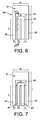
- Figures 6 and 7 are top views of two clamped-free beams bearing a current loop dedicated to thermoelastic actuation and a current loop dedicated to piezoresistive detection, the loops being overlapping. These beams are symmetrical in relation to their longitudinal axis. The part of the beam situated at the top of each figure is free. The part of the beam situated at the bottom of each figure is embedded.
- Figure 6 shows a beam 30 comprising one end 31 capable of moving in a direction perpendicular to the figure plane, a first current loop 32 made of AlSi and a second current loop 33 made of AlSi. In this embodiment example, all of the current loops rest on a silicon layer 34.
- Figure 7 shows a beam 40 comprising one end 41 capable of moving in a direction perpendicular to the figure plane, a first AlSi current loop 42 and a second AlSi current loop 43.
- first AlSi current loop 42 and a second AlSi current loop 43.
- only the parts of the current loops situated towards the end 41 rest on a silicon layer 44.
- Table 3 gives examples of dimensions (in ⁇ m) for the beams represented in figures 6 and 7 .
- Table 3 l w l 1 b 1 b 2 s g 5 1.4 2 0.2 0.2 0.2 1 7 2.1 2.5 0.3 0.3 0.3 1.5
- Figures 8A to 8D are longitudinal sectional views illustrating a method of producing the clamped-free beam of figure 6 . These figures are views along the axis VIII-VIII of figure 6 .
- Figure 8A shows an SOI substrate 50 constituted of a silicon support 51 supporting successively a buried oxide layer 52 and a superficial silicon layer 53.
- An AlSi layer 54 of 50 nm thickness is formed on the superficial layer 53.
- the definition of the silicon part of the beam is then carried out.
- a step of lithography is carried out to leave a protection pad 55 on the part of the superficial silicon layer 53 not covered by the remaining AlSi layer 54 and which is to be conserved (see figure 8C ).
- the etching of the superficial silicon layer 53 is then carried out by a CF 4 based plasma.
- the protection pad 55 is eliminated and the release of the beam is carried out by HF etching of the buried oxide layer 52.
- the structure represented in figure 8D is obtained, where the direction of displacement of the beam is indicated by an arrow.
- Figure 9 is a top view of another clamped-free beam bearing a current loop dedicated to thermoelastic actuation and a current loop dedicated to piezoresistive detection.
- the beam comprises an actuating electric loop 61 connected to the connection pads 62 and 63 and an electric detection loop 64 connected to the connection pads 65 and 66.
- the embedment area of the beam is shown under the reference 67.
- the reference 68 designates a part of thin silicon film remaining under the free part of the beam.
- bridges clamped-clamped beams
- Figures 10A and 10B are views respectively in longitudinal section and top section of a clamped-clamped beam with an actuation loop to one embedment and a detection loop to the other embedment.
- the structure shown in figures 10A and 10B is formed from an SOI substrate 70 comprising support 71 supporting successively a buried oxide layer 72 and a superficial silicon layer 73.
- the part 74 of the beam, made of silicon, is obtained by photolithography and by plasma etching of the superficial silicon layer 73 then by HF etching of the buried oxide layer 72.
- Depositions of AlSi are formed on the beam to obtain an actuation loop 75 to one of the embedments and a detection loop 76 to the other embedment.
- Table 4 gives examples of dimensions (in ⁇ m) for the clamped-clamped beam represented in figures 10A and 10B .
- Table 4 l w b s z d f o 1 0.22 1 400 1.1 0.34 0.08 0.05 0.25 0.08 1 156 1.2 0.27 972 1.3 0.29 828 1.5 0.34 0.08 0.05 0.34 0.08 622 2 0.34 0.08 0.05 0.45 0.08 350 2.5 0.34 0.08 0.05 0.56 0.08 224 3.5 0.34 0.08 0.05 0.46 0.08 114
- This table moreover gives the values of the resonance frequency of the beam (in MHz).
- the AlSi metallic gauge is compressed or expanded as a function of a beam that is connected to it (see figure 11 ).
- This detection model has been disclosed in the document FR-A-2 917 731 .
- the active part of the gauge according to the present invention is not made of silicon. Silicon is only a non-conducting, or weakly conducting, mechanical support compared to the deposited AlSi metallic layer. The gauge is thus the layer of AlSi. If the gauge factor is in this case lower, the Johnson white noise induced by the gauge is on the other hand much weaker, which makes it possible to improve the intrinsic resolution of the sensor.
- Figure 11 schematically represents such a structure in top view. It shows a movable beam 80 embedded in the substrate by one of its ends, the other end being free. Parallel to the movable beam 80 and on the side of its free end is found an actuating electrode 81. Perpendicularly to the movable beam 80 and on the side of its embedded end are found two piezoresistive gauges 82 and 83, each being attached on the one side to the movable beam 80 and on the other side to the substrate.
- the movable beam 80, the actuation electrode 81 and the piezoelectric gauges 82 and 83 are made of silicon covered with AlSi.
- the double arrow indicates the direction of displacement of the movable beam 80.
- Table 5 gives examples of dimensions ( ⁇ m) for the structure represented in figure 11 .
- Table 5 l w l 1 b s a g 6 0.1 3 0.2 0.08 4 0.2 6 0.1 3 0.5 0.08 4 0.2 6 0.2 3 0.2 0.08 4 0.1
- a first deposition is carried out by sputtering at a temperature of 175°C.
- the AlSi layer formed may be formed either via a continuous deposition at constant power, or in several steps, for example in two stages, according to the requisite thickness.
- a first layer of several tens of nanometres may be deposited with a power of 3 kW for example (or 1.5 kW), enabling a quite dense and quite uniform (from 20 to 40 nm) layer to be obtained.
- a second layer may then be added at low power (for example 0.5 kW) in order to better control the final thickness (50 to 60 nm in the end).
- High temperature depositions make it possible to reveal preferential crystalline orientations of the AlSi grains.
- a second type of deposition may also be carried out via a low temperature method at 20°C for example. This makes it possible to obtain smaller grains of AlSi and finer discontinuities between grains with a more homogeneous distribution. These low temperature depositions also make it possible to reduce the roughness of the films of AlSi (by a factor 5, around 1 nm rms in other words root mean square) but increase the resistivity of the material (0.5 to 1 ⁇ ohm.cm) at constant thickness.
- Variable thicknesses can be obtained. For example, the feasibility of uniform and continuous depositions up to 10 nm at least has been demonstrated experimentally. Thicknesses of 80 nm have also been obtained on NEMS. Higher thicknesses may be deposited (100 nm, 200 nm, 500 nm) but it is aimed rather to favour thin films (range from 10 to 100 nm).
- Figure 12 corresponds to a measurement of the resonance peak in ambient air.
- Figure 13 corresponds to a measurement of the resonance peak under a vacuum of 10 -3 torrs.
- the Y-axis of these graphs corresponds to the voltage in volts of the output signal of the means of detection.
- the X-axis corresponds to the frequency f of the signal detected.
- the quality factor Q is equal to 200.
- the quality factor Q is equal to 1100.
- gauge factors between 2 and 4 are found experimentally for AlSi for a resistance of 20 ⁇ , in other words conforming to the known predictions for a metal other than aluminium.
- the resistivities measured are between 3 and 5 ⁇ ohms.cm, according to the thickness considered (around 3 ⁇ ohms.cm for thick films known as "bulk” and close to 4.5 ⁇ ohms.cm for thicknesses of 60 nm).
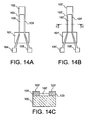
- Figures 14A to 14C illustrate the formation of a piezoresistive sensor for the detection of gas, according to the present invention.
- Figure 14A shows, in top view, the sensor before its functionalization. It comprises a clamped-free silicon beam 100.
- the beam 100 is embedded on a support substrate by the anchoring 101.
- the free end of the beam 100 is covered with a layer of AlSi 102 connected by a current loop 103 to current inputs 104 and 105.
- Figure 14B shows, in top view, the sensor after its functionalization. Its upper surface is covered with a grafting layer spread out in 100' on the silicon beam, in 102' on the layer of AlSi and in 103' on the current loop. The grafting layer also covers in 101' the anchoring of the sensor and in 104' and 105' the current inputs.
- Figure 14C is a transversal sectional view along the axis C-C of figure 14B . This figure shows the distributions of the grafting layer on the different parts of the sensor.
- an accelerometer it is possible for example to use the structure illustrated in figure 11 as a basis. To these structures must be added a test mass, the movement of which will be a function of an external acceleration. The detection may be through compression/traction of the metallic gauge as shown in figure 15 . A test mass undergoing an acceleration is going to constrain the gauge placed perpendicularly to the movement created by the acceleration. The reading is then carried out preferentially with a Wheatstone bridge type measuring bridge. The reading can be made in direct current or in alternating current in order to eliminate the noises in 1/f.
- Figure 15 is a schematic representation of an acceleration sensor using the compression/traction of a strain gauge, according to the invention.
- This figure shows a test mass 110 subjected to an acceleration ⁇ .
- the test mass is connected to anchoring areas 111 and 112 by suspensions 113 and 114.
- the reference 115 designates a strain gauge between the test mass 110 and an anchoring area 116.
- the gauge 115 comprises a layer of AlSi deposited on a nano-silicon beam.
- the thickness of the AlSi layer may be between 10 nm and 200 nm.
- the width of the layer is less than, for example, 100 nm.
- the length to height ratio value of the resonator is for example around 100.
- the gauge can also serve to measure the frequency variation.
- the movement undergone by the beam is going to induce a strain in a vibrating nano-beam judiciously attached to the test mass. This strain is then going to modulate the resonance frequency. This is measured by AlSi metallised strain gauges and placed perpendicularly to the resonating beam as shown in figures 16 and 17 .
- the AlSi gauge works in traction/compression.
- FIG 16 is a schematic representation of an acceleration sensor with frequency detection using a strain gauge working in traction/compression, according to the invention.
- This figure shows a test mass 120 subjected to an acceleration ⁇ .
- the test mass is connected to anchoring areas 121 and 122 by suspensions 123 and 124.
- the reference 125 designates a resonator arranged between the test mass 120 and an anchoring area 126.
- Actuating electrodes, designated under the single reference 127, are arranged to activate the resonator 125.
- a strain gauge 128 is arranged between the resonator 125 and an anchoring area 129 and perpendicularly to the resonator. It works in traction/compression.
- the resonator can have a thickness of silicon for example between 100 nm and 2 ⁇ m. Its width is greater than or equal to 100 nm. The length to height ratio of the resonator is situated around 100. Its spacing in relation to the actuating electrodes is equal to or greater than 50 nm. Its aspect ratio is equal to or greater than 4.
- the strain gauge 128 comprises a layer of AlSi, from 10 nm to 200 nm thickness, deposited on a nano-silicon beam. Its width is less than 100 nm. Its length to height ratio is situated around 100, or even less than 100.
- test mass may be formed in the same layer as the gauge. Nevertheless, advantageously this mass is defined in another thicker layer so as to obtain a sufficient inertia.
- FIG. 17 is a representation illustrating the piezoresistive detection of strain gauges according to the invention and for a Wheatstone bridge measurement.
- This diagram shows two test masses 130 and 140 attached to anchoring areas and subjected to an acceleration ⁇ .
- a resonator 131 is arranged between the test mass 130 and an anchoring area. This resonator is subjected to a force F generated by the test mass 130 under the effect of the acceleration.
- Activation electrodes designated under the single reference 132, are arranged parallel to the resonator 131. Situated perpendicular to the resonator is arranged a strain gauge 133 connected by one end to the resonator 131 and by another end to an anchoring area.
- a resonator 141 is arranged between the test mass 140 and an anchoring area. This resonator is subjected to the force F generated by the test mass 140 under the effect of the acceleration.
- Activation electrodes designated under the single reference 142, are arranged parallel to the resonator 141. Situated perpendicularly to the resonator is arranged a strain gauge 143 connected by one end to the resonator 141 and by another end to an anchoring area.
- the Wheatstone bridge is completed by two fixed resistances R arranged in series in a first branch of the bridge, the strain gauges 133 and 143 being connected in series in the second branch of the bridge.
- the bridge is supplied under a voltage E.
- Figure 18 represents the electrical diagram of the Wheatstone bridge implemented in figure 17 .
- VLSI very large scale integration
Landscapes
- Physics & Mathematics (AREA)
- General Physics & Mathematics (AREA)
- Chemical & Material Sciences (AREA)
- Analytical Chemistry (AREA)
- Immunology (AREA)
- Health & Medical Sciences (AREA)
- Biochemistry (AREA)
- General Health & Medical Sciences (AREA)
- Acoustics & Sound (AREA)
- Life Sciences & Earth Sciences (AREA)
- Pathology (AREA)
- Engineering & Computer Science (AREA)
- Computer Hardware Design (AREA)
- Microelectronics & Electronic Packaging (AREA)
- Pressure Sensors (AREA)
- Micromachines (AREA)
Claims (12)
- Elektromechanisches Nanosystem (NEMS), umfassend wenigstens ein festes Teil, das einem Substrat (21) zugeordnet ist, sowie wenigstens ein relativ zu dem Substrat bewegliches Teil (23), wobei das System Transduktionsmittel (24) umfasst, die dazu ausgelegt sind, das bewegliche Teil anzuregen, um ihm eine Bewegung zu verleihen und/oder eine Bewegung des beweglichen Teils zu erfassen, wobei die Transduktionsmittel wenigstens ein elektrisch leitfähiges Transduktionsmaterial umfassen, dadurch gekennzeichnet, dass das elektrisch leitfähige Transduktionsmaterial aus einer Abscheidung auf Basis einer AlSi-Legierung hergestellt ist, wobei die Abscheidung wenigstens teilweise durch das bewegliche Teil des Systems getragen wird.
- System nach Anspruch 1, wobei die Abscheidung auf Basis der AlSi-Legierung eine Legierung ist, die aus AlSi und AlCuSi ausgewählt ist.
- System nach einem der Ansprüche 1 oder 2, wobei die Transduktionsmittel ferner unter dem elektrisch leitfähigen Material eine Zusatzschicht (56) umfassen, um das elektrisch leitfähige Material zu strukturieren und/oder die erfasste Bewegung zu verstärken und/oder eine Barriere für die Diffusion des leitfähigen Materials zu bilden.
- System nach einem der Ansprüche 1-3, wobei die Abscheidung auf Basis der AlSi-Legierung wenigstens eine Stromschleife für die Anregung des beweglichen Teils und/oder für die Erfassung einer Bewegung des beweglichen Teils bildet.
- System nach Anspruch 4, wobei die Abscheidung auf Basis der AlSi-Legierung zwei überlappende Stromschleifen (32,33) bildet, eine für die Anregung des beweglichen Teils und die andere für die Erfassung einer Bewegung des beweglichen Teils.
- System nach einem der Ansprüche 1-5, wobei das bewegliche Teil des Systems einen Klemm-Frei-Balken oder einen Klemm-Klemm-Balken umfasst.
- System nach einem der Ansprüche 1-6, wobei das Substrat (20, 50,70) einen Träger (21, 51,71) umfasst, der aufeinanderfolgend durch eine elektrisch isolierende Schicht (22, 52,72) und eine Oberflächen-Siliziumschicht (23, 53,73) bedeckt ist, wobei das feste und das bewegliche Teil in der Oberflächen-Siliziumschicht gebildet sind, wobei das bewegliche Teil mittels einer Aushöhlung erhalten ist, die in der elektrisch isolierenden Schicht gebildet ist.
- System nach einem der Ansprüche 1-4, wobei das System ferner eine Testmasse (110) umfasst, wobei das bewegliche Teile (115) mittels eines seiner Enden an dem Substrat und mittels seines anderen Endes an der Testmasse angebracht ist, wobei die Transduktionsmittel Mittel sind, die dazu ausgelegt sind, eine Bewegung zu erfassen.
- System nach einem der Ansprüche 1-4, wobei das System ferner eine Testmasse (120) umfasst, wobei ein Resonator (125) die Testmasse mit dem Substrat verbindet, wobei das bewegliche Teil (128) mittels eines seiner Enden an dem Substrat und mittels seines anderen Endes an dem Resonator angebracht ist, wobei die Transduktionsmittel Mittel sind, die dazu ausgelegt sind, eine Beschleunigung zu erfassen.
- System nach einem der Ansprüche 1-9, wobei die Abscheidung auf Basis der AlSi-Legierung eine Dicke zwischen 10 und 100 nm hat, vorzugsweise zwischen 40 und 80 nm.
- System nach einem der Ansprüche 1-10, ferner umfassend wenigstens eine Abscheidung einer elektrogepfropften Funktionalisierungsschicht jenseits des Materials auf Basis der AlSi-Legierung.
- Sensor, umfassend das System nach Anspruch 1, wobei der Sensor ein Massensensor, ein Gassensor, ein biochemischer Sensor, ein Kraftsensor, ein Trägheitssensor oder ein Drucksensor ist.
Applications Claiming Priority (3)
| Application Number | Priority Date | Filing Date | Title |
|---|---|---|---|
| FR0954998A FR2948114B1 (fr) | 2009-07-17 | 2009-07-17 | Nems comportant des moyens de transduction a base d'alliage d'aluminium |
| US22641909P | 2009-09-17 | 2009-09-17 | |
| PCT/EP2010/060033 WO2011006885A1 (en) | 2009-07-17 | 2010-07-13 | Nems comprising alsi alloy based transduction means |
Publications (2)
| Publication Number | Publication Date |
|---|---|
| EP2454573A1 EP2454573A1 (de) | 2012-05-23 |
| EP2454573B1 true EP2454573B1 (de) | 2013-12-04 |
Family
ID=41630775
Family Applications (1)
| Application Number | Title | Priority Date | Filing Date |
|---|---|---|---|
| EP10731526.9A Not-in-force EP2454573B1 (de) | 2009-07-17 | 2010-07-13 | Nems mit transduktionsvorrichtung auf der basis einer al-si-legierung |
Country Status (4)
| Country | Link |
|---|---|
| US (1) | US9016125B2 (de) |
| EP (1) | EP2454573B1 (de) |
| FR (1) | FR2948114B1 (de) |
| WO (1) | WO2011006885A1 (de) |
Cited By (3)
| Publication number | Priority date | Publication date | Assignee | Title |
|---|---|---|---|---|
| CN104671186A (zh) * | 2013-11-27 | 2015-06-03 | 英飞凌科技股份有限公司 | Mems器件 |
| CN105974104A (zh) * | 2016-05-12 | 2016-09-28 | 南京信息工程大学 | 基于巨压阻结构的悬臂梁生化传感器及悬臂梁制作方法 |
| CN106829852A (zh) * | 2017-01-18 | 2017-06-13 | 中国科学院深圳先进技术研究院 | L型静电驱动微型机器人、制造方法与控制方法 |
Families Citing this family (17)
| Publication number | Priority date | Publication date | Assignee | Title |
|---|---|---|---|---|
| WO2008039372A2 (en) * | 2006-09-22 | 2008-04-03 | Carnegie Mellon University | Assembling and applying nano-electro-mechanical systems |
| FR2950698B1 (fr) * | 2009-09-25 | 2012-03-23 | Commissariat Energie Atomique | Dispositif de detection de gaz et/ou de composes organiques volatils (cov) |
| RU2533325C2 (ru) * | 2011-03-15 | 2014-11-20 | Закрытое Акционерное Общество "Нанотехнология Мдт" | Многофункциональная сенсорная микроэлектромеханическая система |
| US9347815B2 (en) | 2012-05-09 | 2016-05-24 | California Institute Of Technology | Single-protein nanomechanical mass spectrometry in real time |
| FR2995691B1 (fr) | 2012-09-19 | 2014-10-10 | Commissariat Energie Atomique | Capteur de flux thermique, capteur de gaz comportant au moins un tel capteur et jauge pirani comportant au moins un tel capteur |
| US9660654B2 (en) | 2012-10-26 | 2017-05-23 | California Institute Of Technology | Synchronization of nanomechanical oscillators |
| WO2014107173A1 (en) | 2013-01-02 | 2014-07-10 | California Institute Of Technology | Piezoresistive nems resonator array |
| WO2014130095A2 (en) | 2013-02-22 | 2014-08-28 | California Institute Of Technology | Shape analysis and mass spectrometry of individual molecules by nanomechanical systems |
| US9360495B1 (en) | 2013-03-14 | 2016-06-07 | Lockheed Martin Corporation | Low density underwater accelerometer |
| FR3008690B1 (fr) | 2013-07-22 | 2016-12-23 | Commissariat Energie Atomique | Dispositif comportant un canal fluidique muni d'au moins un systeme micro ou nanoelectronique et procede de realisation d'un tel dispositif |
| FR3008691B1 (fr) | 2013-07-22 | 2016-12-23 | Commissariat Energie Atomique | Dispositif comportant un canal fluidique muni d'au moins un systeme micro ou nanoelectronique et procede de realisation d'un tel dispositif |
| FR3011835B1 (fr) | 2013-10-16 | 2015-12-25 | Commissariat Energie Atomique | Procede de realisation par voie electrochimique d'au moins une zone poreuse d'une structure micro et/ou nanoelectronique |
| FR3017463B1 (fr) | 2014-02-13 | 2020-11-13 | Commissariat Energie Atomique | Capteur de concentration de gaz a structure suspendue |
| CN110718442B (zh) | 2015-01-23 | 2022-08-16 | 加州理工学院 | 整合的混合nems质谱测定法 |
| CN109991444A (zh) * | 2017-12-30 | 2019-07-09 | 大连良华科技有限公司 | 一种应变式加速度传感器 |
| US11289319B2 (en) | 2019-08-06 | 2022-03-29 | Thermo Fisher Scientific (Bremen) Gmbh | System to analyze particles, and particularly the mass of particles |
| US11650110B2 (en) * | 2020-11-04 | 2023-05-16 | Honeywell International Inc. | Rosette piezo-resistive gauge circuit for thermally compensated measurement of full stress tensor |
Family Cites Families (7)
| Publication number | Priority date | Publication date | Assignee | Title |
|---|---|---|---|---|
| JPS61239644A (ja) | 1985-04-16 | 1986-10-24 | Oki Electric Ind Co Ltd | 半導体装置多層配線の製造方法 |
| DE10051315A1 (de) * | 2000-10-17 | 2002-04-18 | Bosch Gmbh Robert | Mikromechanisches Bauelement und entsprechendes Hersellungsverfahren |
| US7434476B2 (en) * | 2003-05-07 | 2008-10-14 | Califronia Institute Of Technology | Metallic thin film piezoresistive transduction in micromechanical and nanomechanical devices and its application in self-sensing SPM probes |
| GB0605273D0 (en) * | 2006-03-16 | 2006-04-26 | Council Cent Lab Res Councils | Fluid robe |
| FR2917731B1 (fr) | 2007-06-25 | 2009-10-23 | Commissariat Energie Atomique | Dispositif resonant a detection piezoresistive realise en technologies de surface |
| US7784344B2 (en) * | 2007-11-29 | 2010-08-31 | Honeywell International Inc. | Integrated MEMS 3D multi-sensor |
| FR2929464B1 (fr) * | 2008-03-28 | 2011-09-09 | Commissariat Energie Atomique | Nano resonnateur magnetique |
-
2009
- 2009-07-17 FR FR0954998A patent/FR2948114B1/fr not_active Expired - Fee Related
-
2010
- 2010-07-13 EP EP10731526.9A patent/EP2454573B1/de not_active Not-in-force
- 2010-07-13 WO PCT/EP2010/060033 patent/WO2011006885A1/en not_active Ceased
- 2010-07-13 US US13/384,474 patent/US9016125B2/en active Active
Cited By (5)
| Publication number | Priority date | Publication date | Assignee | Title |
|---|---|---|---|---|
| CN104671186A (zh) * | 2013-11-27 | 2015-06-03 | 英飞凌科技股份有限公司 | Mems器件 |
| CN105974104A (zh) * | 2016-05-12 | 2016-09-28 | 南京信息工程大学 | 基于巨压阻结构的悬臂梁生化传感器及悬臂梁制作方法 |
| CN105974104B (zh) * | 2016-05-12 | 2017-12-15 | 南京信息工程大学 | 基于巨压阻结构的悬臂梁生化传感器及悬臂梁制作方法 |
| CN106829852A (zh) * | 2017-01-18 | 2017-06-13 | 中国科学院深圳先进技术研究院 | L型静电驱动微型机器人、制造方法与控制方法 |
| CN106829852B (zh) * | 2017-01-18 | 2018-05-04 | 中国科学院深圳先进技术研究院 | L型静电驱动微型机器人、制造方法与控制方法 |
Also Published As
| Publication number | Publication date |
|---|---|
| FR2948114B1 (fr) | 2012-03-30 |
| FR2948114A1 (fr) | 2011-01-21 |
| EP2454573A1 (de) | 2012-05-23 |
| WO2011006885A1 (en) | 2011-01-20 |
| US9016125B2 (en) | 2015-04-28 |
| US20120272742A1 (en) | 2012-11-01 |
Similar Documents
| Publication | Publication Date | Title |
|---|---|---|
| US9016125B2 (en) | NEMS comprising AlSi alloy based transducer | |
| Chasiotis et al. | Strain rate effects on the mechanical behavior of nanocrystalline Au films | |
| US11228294B2 (en) | Graphene microelectromechanical system (MEMS) resonant gas sensor | |
| EP2579010B1 (de) | Oberflächenbelastungssensor | |
| US6441716B1 (en) | Semiconductor piezoresistor | |
| EP1987336B1 (de) | Mit interner anspannung betätigte mikro- und nanomaschinen zum prüfen physikalischer eigenschaften von materialproben mit mikro- und nanogrösse | |
| Saleem et al. | A systematic review of reliability issues in RF-MEMS switches | |
| US8302494B2 (en) | Sensor for quantitative measurement of electromechanical properties and microstructure of nano-materials and method for making the same | |
| US20090038404A1 (en) | Metallic thin film piezoresistive transduction in micromechanical and nanomechanical devices and its application in self-sensing spm probes | |
| JP2009133862A (ja) | ひずみ増幅セルを有する吊るされたピエゾ抵抗のひずみゲージによる検出器を有する装置 | |
| US9382108B2 (en) | Nanowire sensor device | |
| Arora et al. | Design of mems based microcantilever using comsol multiphysics | |
| Johns | Modeling piezoresistivity in silicon and polysilicon | |
| Sparks et al. | Cyclic fatigue and creep of electroformed micromachines | |
| Tina et al. | Silicon MEMS nanomechanical membrane flexure sensor with integrated high gauge factor ITO | |
| Cianci et al. | Young’s modulus and residual stress of DF PECVD silicon nitride for MEMS free-standing membranes | |
| EP2862000B1 (de) | Sensor für magnetfelder mit laplace-kraft | |
| Mohanasundaram et al. | Tuning the sensitivity of a metal-based piezoresistive sensor using electromigration | |
| Johansson et al. | Temperature effects in Au piezoresistors integrated in SU-8 cantilever chips | |
| Pratap et al. | Effect of microfabrication induced stresses on the sensing characteristics of dynamic MEMS devices | |
| Samuel et al. | Room temperature relaxation of freestanding nanocrystalline gold films | |
| Lu et al. | Design, fabrication, and integration of piezoelectric MEMS devices for applications in wireless sensor network | |
| Zwijze et al. | Low-cost piezoresistive silicon load cell independent of force distribution | |
| Fraga et al. | Fabrication and characterization of piezoresistive strain sensors for high temperature applications | |
| Hwang et al. | Flexible polysilicon strain gauge array |
Legal Events
| Date | Code | Title | Description |
|---|---|---|---|
| PUAI | Public reference made under article 153(3) epc to a published international application that has entered the european phase |
Free format text: ORIGINAL CODE: 0009012 |
|
| 17P | Request for examination filed |
Effective date: 20120117 |
|
| AK | Designated contracting states |
Kind code of ref document: A1 Designated state(s): AL AT BE BG CH CY CZ DE DK EE ES FI FR GB GR HR HU IE IS IT LI LT LU LV MC MK MT NL NO PL PT RO SE SI SK SM TR |
|
| DAX | Request for extension of the european patent (deleted) | ||
| GRAP | Despatch of communication of intention to grant a patent |
Free format text: ORIGINAL CODE: EPIDOSNIGR1 |
|
| INTG | Intention to grant announced |
Effective date: 20130517 |
|
| GRAS | Grant fee paid |
Free format text: ORIGINAL CODE: EPIDOSNIGR3 |
|
| GRAA | (expected) grant |
Free format text: ORIGINAL CODE: 0009210 |
|
| AK | Designated contracting states |
Kind code of ref document: B1 Designated state(s): AL AT BE BG CH CY CZ DE DK EE ES FI FR GB GR HR HU IE IS IT LI LT LU LV MC MK MT NL NO PL PT RO SE SI SK SM TR |
|
| REG | Reference to a national code |
Ref country code: GB Ref legal event code: FG4D |
|
| REG | Reference to a national code |
Ref country code: CH Ref legal event code: EP |
|
| REG | Reference to a national code |
Ref country code: AT Ref legal event code: REF Ref document number: 643713 Country of ref document: AT Kind code of ref document: T Effective date: 20140115 Ref country code: IE Ref legal event code: FG4D |
|
| REG | Reference to a national code |
Ref country code: DE Ref legal event code: R096 Ref document number: 602010012201 Country of ref document: DE Effective date: 20140130 |
|
| REG | Reference to a national code |
Ref country code: NL Ref legal event code: VDEP Effective date: 20131204 |
|
| REG | Reference to a national code |
Ref country code: AT Ref legal event code: MK05 Ref document number: 643713 Country of ref document: AT Kind code of ref document: T Effective date: 20131204 |
|
| PG25 | Lapsed in a contracting state [announced via postgrant information from national office to epo] |
Ref country code: LT Free format text: LAPSE BECAUSE OF FAILURE TO SUBMIT A TRANSLATION OF THE DESCRIPTION OR TO PAY THE FEE WITHIN THE PRESCRIBED TIME-LIMIT Effective date: 20131204 Ref country code: NO Free format text: LAPSE BECAUSE OF FAILURE TO SUBMIT A TRANSLATION OF THE DESCRIPTION OR TO PAY THE FEE WITHIN THE PRESCRIBED TIME-LIMIT Effective date: 20140304 Ref country code: FI Free format text: LAPSE BECAUSE OF FAILURE TO SUBMIT A TRANSLATION OF THE DESCRIPTION OR TO PAY THE FEE WITHIN THE PRESCRIBED TIME-LIMIT Effective date: 20131204 Ref country code: SE Free format text: LAPSE BECAUSE OF FAILURE TO SUBMIT A TRANSLATION OF THE DESCRIPTION OR TO PAY THE FEE WITHIN THE PRESCRIBED TIME-LIMIT Effective date: 20131204 Ref country code: HR Free format text: LAPSE BECAUSE OF FAILURE TO SUBMIT A TRANSLATION OF THE DESCRIPTION OR TO PAY THE FEE WITHIN THE PRESCRIBED TIME-LIMIT Effective date: 20131204 Ref country code: NL Free format text: LAPSE BECAUSE OF FAILURE TO SUBMIT A TRANSLATION OF THE DESCRIPTION OR TO PAY THE FEE WITHIN THE PRESCRIBED TIME-LIMIT Effective date: 20131204 |
|
| REG | Reference to a national code |
Ref country code: LT Ref legal event code: MG4D |
|
| PG25 | Lapsed in a contracting state [announced via postgrant information from national office to epo] |
Ref country code: LV Free format text: LAPSE BECAUSE OF FAILURE TO SUBMIT A TRANSLATION OF THE DESCRIPTION OR TO PAY THE FEE WITHIN THE PRESCRIBED TIME-LIMIT Effective date: 20131204 Ref country code: AT Free format text: LAPSE BECAUSE OF FAILURE TO SUBMIT A TRANSLATION OF THE DESCRIPTION OR TO PAY THE FEE WITHIN THE PRESCRIBED TIME-LIMIT Effective date: 20131204 Ref country code: CY Free format text: LAPSE BECAUSE OF FAILURE TO SUBMIT A TRANSLATION OF THE DESCRIPTION OR TO PAY THE FEE WITHIN THE PRESCRIBED TIME-LIMIT Effective date: 20131204 |
|
| PG25 | Lapsed in a contracting state [announced via postgrant information from national office to epo] |
Ref country code: BE Free format text: LAPSE BECAUSE OF FAILURE TO SUBMIT A TRANSLATION OF THE DESCRIPTION OR TO PAY THE FEE WITHIN THE PRESCRIBED TIME-LIMIT Effective date: 20131204 Ref country code: EE Free format text: LAPSE BECAUSE OF FAILURE TO SUBMIT A TRANSLATION OF THE DESCRIPTION OR TO PAY THE FEE WITHIN THE PRESCRIBED TIME-LIMIT Effective date: 20131204 Ref country code: IS Free format text: LAPSE BECAUSE OF FAILURE TO SUBMIT A TRANSLATION OF THE DESCRIPTION OR TO PAY THE FEE WITHIN THE PRESCRIBED TIME-LIMIT Effective date: 20140404 |
|
| PG25 | Lapsed in a contracting state [announced via postgrant information from national office to epo] |
Ref country code: SK Free format text: LAPSE BECAUSE OF FAILURE TO SUBMIT A TRANSLATION OF THE DESCRIPTION OR TO PAY THE FEE WITHIN THE PRESCRIBED TIME-LIMIT Effective date: 20131204 Ref country code: ES Free format text: LAPSE BECAUSE OF FAILURE TO SUBMIT A TRANSLATION OF THE DESCRIPTION OR TO PAY THE FEE WITHIN THE PRESCRIBED TIME-LIMIT Effective date: 20131204 Ref country code: PT Free format text: LAPSE BECAUSE OF FAILURE TO SUBMIT A TRANSLATION OF THE DESCRIPTION OR TO PAY THE FEE WITHIN THE PRESCRIBED TIME-LIMIT Effective date: 20140404 Ref country code: PL Free format text: LAPSE BECAUSE OF FAILURE TO SUBMIT A TRANSLATION OF THE DESCRIPTION OR TO PAY THE FEE WITHIN THE PRESCRIBED TIME-LIMIT Effective date: 20131204 Ref country code: CZ Free format text: LAPSE BECAUSE OF FAILURE TO SUBMIT A TRANSLATION OF THE DESCRIPTION OR TO PAY THE FEE WITHIN THE PRESCRIBED TIME-LIMIT Effective date: 20131204 Ref country code: RO Free format text: LAPSE BECAUSE OF FAILURE TO SUBMIT A TRANSLATION OF THE DESCRIPTION OR TO PAY THE FEE WITHIN THE PRESCRIBED TIME-LIMIT Effective date: 20131204 |
|
| REG | Reference to a national code |
Ref country code: DE Ref legal event code: R097 Ref document number: 602010012201 Country of ref document: DE |
|
| PLBE | No opposition filed within time limit |
Free format text: ORIGINAL CODE: 0009261 |
|
| STAA | Information on the status of an ep patent application or granted ep patent |
Free format text: STATUS: NO OPPOSITION FILED WITHIN TIME LIMIT |
|
| PG25 | Lapsed in a contracting state [announced via postgrant information from national office to epo] |
Ref country code: DK Free format text: LAPSE BECAUSE OF FAILURE TO SUBMIT A TRANSLATION OF THE DESCRIPTION OR TO PAY THE FEE WITHIN THE PRESCRIBED TIME-LIMIT Effective date: 20131204 |
|
| 26N | No opposition filed |
Effective date: 20140905 |
|
| REG | Reference to a national code |
Ref country code: DE Ref legal event code: R097 Ref document number: 602010012201 Country of ref document: DE Effective date: 20140905 |
|
| PG25 | Lapsed in a contracting state [announced via postgrant information from national office to epo] |
Ref country code: SI Free format text: LAPSE BECAUSE OF FAILURE TO SUBMIT A TRANSLATION OF THE DESCRIPTION OR TO PAY THE FEE WITHIN THE PRESCRIBED TIME-LIMIT Effective date: 20131204 Ref country code: LU Free format text: LAPSE BECAUSE OF FAILURE TO SUBMIT A TRANSLATION OF THE DESCRIPTION OR TO PAY THE FEE WITHIN THE PRESCRIBED TIME-LIMIT Effective date: 20140713 |
|
| REG | Reference to a national code |
Ref country code: CH Ref legal event code: PL |
|
| REG | Reference to a national code |
Ref country code: IE Ref legal event code: MM4A |
|
| PG25 | Lapsed in a contracting state [announced via postgrant information from national office to epo] |
Ref country code: IT Free format text: LAPSE BECAUSE OF FAILURE TO SUBMIT A TRANSLATION OF THE DESCRIPTION OR TO PAY THE FEE WITHIN THE PRESCRIBED TIME-LIMIT Effective date: 20131204 Ref country code: LI Free format text: LAPSE BECAUSE OF NON-PAYMENT OF DUE FEES Effective date: 20140731 Ref country code: CH Free format text: LAPSE BECAUSE OF NON-PAYMENT OF DUE FEES Effective date: 20140731 |
|
| PG25 | Lapsed in a contracting state [announced via postgrant information from national office to epo] |
Ref country code: IE Free format text: LAPSE BECAUSE OF NON-PAYMENT OF DUE FEES Effective date: 20140713 |
|
| PG25 | Lapsed in a contracting state [announced via postgrant information from national office to epo] |
Ref country code: SM Free format text: LAPSE BECAUSE OF FAILURE TO SUBMIT A TRANSLATION OF THE DESCRIPTION OR TO PAY THE FEE WITHIN THE PRESCRIBED TIME-LIMIT Effective date: 20131204 Ref country code: MC Free format text: LAPSE BECAUSE OF FAILURE TO SUBMIT A TRANSLATION OF THE DESCRIPTION OR TO PAY THE FEE WITHIN THE PRESCRIBED TIME-LIMIT Effective date: 20131204 |
|
| PG25 | Lapsed in a contracting state [announced via postgrant information from national office to epo] |
Ref country code: GR Free format text: LAPSE BECAUSE OF FAILURE TO SUBMIT A TRANSLATION OF THE DESCRIPTION OR TO PAY THE FEE WITHIN THE PRESCRIBED TIME-LIMIT Effective date: 20140305 Ref country code: BG Free format text: LAPSE BECAUSE OF FAILURE TO SUBMIT A TRANSLATION OF THE DESCRIPTION OR TO PAY THE FEE WITHIN THE PRESCRIBED TIME-LIMIT Effective date: 20131204 Ref country code: MT Free format text: LAPSE BECAUSE OF FAILURE TO SUBMIT A TRANSLATION OF THE DESCRIPTION OR TO PAY THE FEE WITHIN THE PRESCRIBED TIME-LIMIT Effective date: 20131204 |
|
| PG25 | Lapsed in a contracting state [announced via postgrant information from national office to epo] |
Ref country code: TR Free format text: LAPSE BECAUSE OF FAILURE TO SUBMIT A TRANSLATION OF THE DESCRIPTION OR TO PAY THE FEE WITHIN THE PRESCRIBED TIME-LIMIT Effective date: 20131204 Ref country code: HU Free format text: LAPSE BECAUSE OF FAILURE TO SUBMIT A TRANSLATION OF THE DESCRIPTION OR TO PAY THE FEE WITHIN THE PRESCRIBED TIME-LIMIT; INVALID AB INITIO Effective date: 20100713 |
|
| REG | Reference to a national code |
Ref country code: FR Ref legal event code: PLFP Year of fee payment: 7 |
|
| REG | Reference to a national code |
Ref country code: FR Ref legal event code: PLFP Year of fee payment: 8 |
|
| PG25 | Lapsed in a contracting state [announced via postgrant information from national office to epo] |
Ref country code: MK Free format text: LAPSE BECAUSE OF FAILURE TO SUBMIT A TRANSLATION OF THE DESCRIPTION OR TO PAY THE FEE WITHIN THE PRESCRIBED TIME-LIMIT Effective date: 20131204 |
|
| REG | Reference to a national code |
Ref country code: FR Ref legal event code: PLFP Year of fee payment: 9 |
|
| PG25 | Lapsed in a contracting state [announced via postgrant information from national office to epo] |
Ref country code: AL Free format text: LAPSE BECAUSE OF FAILURE TO SUBMIT A TRANSLATION OF THE DESCRIPTION OR TO PAY THE FEE WITHIN THE PRESCRIBED TIME-LIMIT Effective date: 20131204 |
|
| PGFP | Annual fee paid to national office [announced via postgrant information from national office to epo] |
Ref country code: DE Payment date: 20240719 Year of fee payment: 15 |
|
| PGFP | Annual fee paid to national office [announced via postgrant information from national office to epo] |
Ref country code: GB Payment date: 20240722 Year of fee payment: 15 |
|
| PGFP | Annual fee paid to national office [announced via postgrant information from national office to epo] |
Ref country code: FR Payment date: 20240723 Year of fee payment: 15 |
|
| REG | Reference to a national code |
Ref country code: DE Ref legal event code: R119 Ref document number: 602010012201 Country of ref document: DE |
|
| GBPC | Gb: european patent ceased through non-payment of renewal fee |
Effective date: 20250713 |
|
| PG25 | Lapsed in a contracting state [announced via postgrant information from national office to epo] |
Ref country code: GB Free format text: LAPSE BECAUSE OF NON-PAYMENT OF DUE FEES Effective date: 20250713 |
|
| PG25 | Lapsed in a contracting state [announced via postgrant information from national office to epo] |
Ref country code: DE Free format text: LAPSE BECAUSE OF NON-PAYMENT OF DUE FEES Effective date: 20260203 |
|
| PG25 | Lapsed in a contracting state [announced via postgrant information from national office to epo] |
Ref country code: FR Free format text: LAPSE BECAUSE OF NON-PAYMENT OF DUE FEES Effective date: 20250731 |