EP2451006A1 - Portable radio - Google Patents
Portable radio Download PDFInfo
- Publication number
- EP2451006A1 EP2451006A1 EP10806163A EP10806163A EP2451006A1 EP 2451006 A1 EP2451006 A1 EP 2451006A1 EP 10806163 A EP10806163 A EP 10806163A EP 10806163 A EP10806163 A EP 10806163A EP 2451006 A1 EP2451006 A1 EP 2451006A1
- Authority
- EP
- European Patent Office
- Prior art keywords
- antenna
- casing
- circuit
- disposed
- elastic member
- Prior art date
- Legal status (The legal status is an assumption and is not a legal conclusion. Google has not performed a legal analysis and makes no representation as to the accuracy of the status listed.)
- Withdrawn
Links
Images


Classifications
-
- H—ELECTRICITY
- H01—ELECTRIC ELEMENTS
- H01Q—ANTENNAS, i.e. RADIO AERIALS
- H01Q1/00—Details of, or arrangements associated with, antennas
- H01Q1/40—Radiating elements coated with or embedded in protective material
-
- H—ELECTRICITY
- H01—ELECTRIC ELEMENTS
- H01Q—ANTENNAS, i.e. RADIO AERIALS
- H01Q1/00—Details of, or arrangements associated with, antennas
- H01Q1/04—Adaptation for subterranean or subaqueous use
-
- H—ELECTRICITY
- H01—ELECTRIC ELEMENTS
- H01Q—ANTENNAS, i.e. RADIO AERIALS
- H01Q1/00—Details of, or arrangements associated with, antennas
- H01Q1/12—Supports; Mounting means
- H01Q1/20—Resilient mountings
-
- H—ELECTRICITY
- H01—ELECTRIC ELEMENTS
- H01Q—ANTENNAS, i.e. RADIO AERIALS
- H01Q1/00—Details of, or arrangements associated with, antennas
- H01Q1/12—Supports; Mounting means
- H01Q1/22—Supports; Mounting means by structural association with other equipment or articles
- H01Q1/24—Supports; Mounting means by structural association with other equipment or articles with receiving set
- H01Q1/241—Supports; Mounting means by structural association with other equipment or articles with receiving set used in mobile communications, e.g. GSM
- H01Q1/242—Supports; Mounting means by structural association with other equipment or articles with receiving set used in mobile communications, e.g. GSM specially adapted for hand-held use
- H01Q1/243—Supports; Mounting means by structural association with other equipment or articles with receiving set used in mobile communications, e.g. GSM specially adapted for hand-held use with built-in antennas
-
- H—ELECTRICITY
- H04—ELECTRIC COMMUNICATION TECHNIQUE
- H04M—TELEPHONIC COMMUNICATION
- H04M1/00—Substation equipment, e.g. for use by subscribers
- H04M1/02—Constructional features of telephone sets
- H04M1/18—Telephone sets specially adapted for use in ships, mines, or other places exposed to adverse environment
Definitions
- the present invention relates to a portable wireless device which can be utilized for a cellular phone, a personal digital assistance (PDA), a portable music player, a portable video game player, for example, and in particular relates to a structure for realizing an antenna and electric circuits accompanying therewith and a water proof function each housed within a casing.
- PDA personal digital assistance
- a portable music player for example
- a portable video game player for example, and in particular relates to a structure for realizing an antenna and electric circuits accompanying therewith and a water proof function each housed within a casing.
- the performance of an antenna for wireless communication largely depends on a distance between an antenna element and the ground. That is, each of the radiation resistance and the gain of the antenna reduce according to the reduction of the distance between the antenna element and the ground.
- a printed board mounting electronic circuits thereon actually occupies most of the inner space of the casing. Further, a ground pattern is formed on the printed board.
- the antenna element is usually disposed near the end portion within the casing to thereby enlarge the distance between the antenna element and the ground pattern of the printed board.
- a member such as a water-proof packing is disposed at the end portion of the casing so as to surround the electric circuits such as the printed board.
- the water-proof packing is disposed at the end portion within the casing, the remaining space within the casing becomes narrow due to the packing.
- the antenna element can not be disposed at the end portion of the casing, the antenna element is disposed on the inner side than the packing. As a result, the distance between the antenna element and the printed board becomes small and hence the characteristics of the antenna likely deteriorate.
- the patent literature 1 discloses the configuration that a casing is configured by an upper casing and a lower casing, a water-proof packing of a frame type exists at a coupling portion between the upper casing and the lower casing, and an antenna element is buried within the water-proof packing.
- the patent literature 2 proposes to provide a cut portion at the center portion (position at a length M: length resonating at the second resonance frequency band (f2)) of an antenna pattern having an entire length L and resonating at the first frequency band (f1).
- the cut portion is provided on the linear portion of the antenna pattern.
- a passive element resonating at the second resonance frequency band is provided at the cut portion.
- the antenna element is inevitably disposed in a space on the inner side of the water-proof packing.
- the passive element exists at the center portion of the antenna element, when the antenna element is disposed at a position near the water-proof packing in order to separate the antenna element from the circuit board, the passive element is apt to be sandwiched by the casing and hence the passive element is likely broken.
- An object of this invention is to provide a portable wireless device which has a water-proof function, can prevent the deterioration of the performance of an antenna and also can avoid the mechanical breakage of a circuit part coupled to the antenna.
- the portable wireless device is arranged in a manner that, in the portable wireless device having a casing formed by assembling a first casing and a second casing, the portable wireless device includes: an annular elastic member which is sandwiched between the first casing and the second casing; a flexible printed board which is integrally formed with the annular elastic member and disposed in a region surrounded by the annular elastic member; an antenna part which is disposed on the flexible printed board; a first electric circuit part which is disposed at the antenna part; and a circuit board which is disposed in the region surrounded by the annular elastic member, wherein a portion of the antenna part is disposed along a portion of the annular elastic member, the first electric circuit part is disposed inside of the annular elastic member, and the antenna part and a ground part of the circuit board are separated therebetween with a predetermined length or more.
- the antenna part can be disposed along the annular elastic member, that is, at the portion separated from the ground part of the circuit board within the casing.
- the degradation of the antenna performance can be prevented.
- sine the first electric circuit part is disposed at the antenna part, it becomes possible to adjust the electrical length of the antenna and also adjust the resonance frequency characteristics.
- the portable wireless device further includes a second electric circuit part which is disposed on the circuit board, wherein the first electric circuit part performs impedance matching between the antenna part and the second electric circuit part.
- this portable wireless device it is possible to perform the impedance matching between the antenna part and an electric circuit such as a wireless circuit.
- the portable wireless device is arranged in a manner that the first electric circuit part controls an electrical length of the antenna part.
- this portable wireless device it is possible to match the resonance frequency of the antenna to a desired frequency without changing the physical length of the antenna part.
- the portable wireless device is arranged in a manner that the first electric circuit part includes at least one of an inductance element, a capacitor element and a meander pattern.
- the electrical length of the antenna part can be controlled by the reactance of the first electric circuit part. Further, when a resonance circuit is formed by coupling a plurality of elements in series or parallel, it is possible to constitute the antenna usable in plural frequency bands.
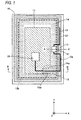
- Fig. 1 is a schematic diagram showing the arrangement state of the main constituent elements within the portable wireless device according to the embodiment.
- Fig. 4 is a perspective view showing an example of the exploded state of the portable wireless device shown in Fig. 1 .
- the portable wireless device shown in Fig. 1 is a cellular phone, for example, which mounts a wireless communication function and an antenna.
- the casing 10 of the portable wireless device has a fixed shape which shape does not change and is configured by assembling, for example, fitting a first casing 11 and a second casing 12 shown in Fig. 4 in the thickness direction (Z-axis direction).
- the casing 10 houses, at the inner space thereof, a circuit board 17 mounting thereon an electric circuit part 18 (second electric circuit part) such as a wireless part, a flexible printed board 14 and an annular elastic member 13, as shown in Fig. 4 .
- the annular elastic member 13 and the flexible printed board 14 are configured as a single component integrated by the one-piece molding.
- the annular elastic member 13 and the flexible printed board 14 can be integrated in a manner that the flexible printed board 14 formed in advance is attached to a predetermined mold, then material of the annular elastic member 13 in a fluid state is flown into the space within the mold and solidified.
- each of the casing 10 and the circuit board 17 is a rectangle, for example.
- the circuit board 17 is housed at the inside of the annular elastic member 13 in the X-Y plane.
- the flexible printed board 14 is formed in an annular shape in this embodiment so as to be able to surround the entire outer periphery of the circuit board 17.
- the contour of each of the outer periphery and the inner periphery of the flexible printed board 14 is formed in a shape close to a rectangle, for example.
- the contour of the inner periphery of the flexible printed board 14 is formed to be slightly larger than the outer periphery of the circuit board 17, whilst the contour of the outer periphery of the flexible printed board 14 is formed to be slightly larger than the contour of the inner periphery thereof.
- the size of the contour of the outer periphery of the flexible printed board 14 is set so as to be able to be housed in the inner space of the casing 10.
- the flexible printed board 14 can be disposed so as to follow the position near the outer periphery of the casing 10, and the circuit board 17 can be disposed at the inside of the inner periphery of the flexible printed board 14.
- the flexible printed board 14 is not necessarily configured to be an annular shape so as to surround the flexible printed board 14 but may be disposed only near a portion where the antenna part 15 is disposed.
- the annular elastic member 13 is a member having elasticity, for example, rubber packing for realizing the water-proof function mainly.
- the annular elastic member 13 has an annular shape as its planar shape like the flexible printed board 14.
- Each of the inner periphery and the outer periphery of the annular elastic member 13 is formed in a rectangle shape in its planar shape, for example.
- the outer periphery of the annular elastic member 13 is larger than the outer periphery of the flexible printed board 14 and the size of the annular elastic member is formed so as to be able to be housed in the inner space of the casing 10.
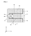
- Fig. 2 is an enlarged constitutional sectional diagram along a line A-A' seen from the Y-axis direction in Fig. 1
- Fig. 3 is a partial plan view of a portion near the line A-A' seen from the Z-axis direction in Fig. 1
- an annular water-proof part 21 and an extension part 22 are integrally formed with the annular elastic member 13.
- the annular water-proof part 21 has a curved surface shape in which each of the upper end and the lower end thereof in the Z-axis direction protrudes at the center portion and has an almost elliptical shape in its section.
- the extension part 22 extends (is provided in an extended manner) from a portion of the annular water-proof part 21 toward the inner peripheral side, that is, in a direction toward the circuit board 17 and is formed in a flat-plate shape.
- the thickness of the annular water-proof part 21 is set to be sufficiently larger than the thickness of the extension part 22.
- the flexible printed board 14 is laminated on and fixed to the extension part 22 in the thickness direction.
- the end portion on the outer peripheral side of the flexible printed board 14 is disposed along the annular water-proof part 21.
- the flexible printed board 14 may be integrated with the annular elastic member 13 in a positional relation that a portion near the end portion on the outer peripheral side of the flexible printed board 14 is buried within the annular water-proof part 21.
- each of an elastic member holding part 11 a formed on the first casing 11 side and an elastic member holding part 12a formed on the second casing 12 side is formed as a concave part having a curved surface so as to follow the shape of the annular water-proof part 21.
- Each of the elastic member holding parts 11 a, 12a is formed in an annular shape so as to match to the shape and size of the annular elastic member 13.
- the antenna part 15 has an antenna pattern 15a which extends linearly along the Y-axis direction.
- a circuit mounting part 19 is coupled near the center of the antenna pattern 15a.
- the circuit mounting part 19 is a circuit element which is provided in order to adjust the electrical length of the antenna part 15 and adjust the resonance frequency characteristics of the antenna part 15.
- the circuit mounting part 19 is disposed on the flexible printed board 14 at a position shifted on the inner peripheral side (position close to the circuit board 17 (see Fig. 1 )) than the antenna pattern 15a.
- the antenna pattern 15a is disposed at a position close to the outer peripheral side than the inner wall 12b of the casing 10.
- the circuit mounting part 19 is disposed at a position close to the inner peripheral side than the inner wall 12b.
- the circuit mounting part 19 is desirably disposed at a position shifted on the inner peripheral side by ⁇ (for example, 0.5 mm) or more than the inner wall 12b.
- circuit mounting part 19 is disposed at the position closer to the ground part of the circuit board 17 as compared with the antenna pattern 15a in the configuration shown in Figs. 1 to 3 , since only a part of the antenna becomes close to the ground part, the characteristics of the antenna scarcely degrades.
- the circuit mounting part 19 has two circuit components 24 (24a, 24b) coupled in parallel. Each of these circuit components is coupled to the antenna pattern 15a via wiring patterns 15b, 15c.
- the circuit components 24 are mounted on the flexible printed board 14 by the reflow soldering, for example. These circuit components 24 are disposed at positions not interfering with the inner wall of the casing 10, that is, within a casing inner space 20 as shown in Fig. 2 .
- a feeding part 16 shown in Fig. 1 is a coupling portion for electrically coupling a wireless part 26 on the circuit board 17 and the antenna part 15 on the flexible printed board 14.
- the feeding part 16 is disposed on the lower end side of the antenna part 15 in the example shown in Fig. 1 .
- An extension part 14a formed so as to protrude on the inner peripheral side is provided at the flexible printed board 14 in the vicinity of the feeding part 16.
- a feeding pattern 15d coupled to the antenna pattern 15a is formed along the extension part 14a.
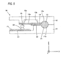
- Fig. 5 (sectional diagram cut along a line B-B' in Fig. 1 ) shows the configuration near the feeding part 16.
- the lower surface side of the flexible printed board 14 abuts against the upper end of a feeding member 23 and the upper surface side of the flexible printed board 14 abuts against the protrusion part 12c of the second casing 12. That is, in the vicinity of the feeding part 16, the flexible printed board 14 is sandwiched between the feeding member 23 and the second casing 12 in the thickness direction (Z-axis direction).
- the feeding member 23 is constituted by conductive material and is fixed on the circuit board 17 in a state of being electrically coupled to a feeding land coupled to the wireless part 26 on the circuit board 17.
- the feeding land 25 is formed at a portion opposing to the tip end portion of the feeding member 23 on the lower surface of the flexible printed board 14 shown in Fig. 5 .
- This feeding land 25 is coupled to the antenna pattern 15a (see Fig. 1 ) via the feeding pattern 15d.
- the electrode (land) on the major surface side of the flexible printed board 14 and the electrode on the rear surface side thereof are electrically coupled via a predetermined through hole.
- the circuit on the circuit board 17 and the antenna part 15 on the flexible printed board 14 are electrically coupled according to the configuration shown in Fig. 5 .
- a ground pattern 27 is formed at a part of the surface area on the circuit board 17.
- the antenna part 15 is configured so as to be separated as far as possible from the ground pattern 27, the radiation resistance of the antenna can be made large and the reduction of the gain can be prevented.
- the distance between the antenna part 15 and the ground pattern 27 can be made large and the reduction of the antenna gain can be prevented.
- the circuit mounting part 19 (first electric circuit part) coupled to the antenna part 15 is provided on the flexible printed board 14, the frequency characteristics of the antenna part 15 can be adjusted. Since the circuit mounting part 19 is disposed on the inner peripheral side than the antenna part 15 and the annular water-proof part 21, the breakage of the components of the circuit mounting part 19 can be prevented without reducing the antenna gain.
- the ground pattern of the circuit board 17 and the antenna part 15 are supposed to be disposed so as to be separated by almost several mm, for example, therebetween. Although this distance is limited by the size of the casing 10 and the size of the vacant space, it is necessary to determine the average distance to be 0.01 ⁇ or more, for example, with respect to the wavelength ⁇ of the radio frequency to be used. Preferably, the distance is determined almost to be in a range from 0.1 ⁇ , to 0.2 ⁇ .
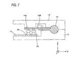
- Fig. 6 is a diagram showing the configuration of the modified example 1 relating to the portable wireless device shown in Fig. 1 .
- Fig. 7 is a sectional diagram showing the configuration near the feeding part along a line C-C' seen from the Y-axis direction in Fig. 6 .
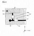
- Fig. 8 is a diagram showing an example of the detailed planar configuration near the feeding part.
- elements correspond to those of Figs. 1 to 5 are marked with the same references, respectively. In this case, the explanation will be mainly made as to modified configuration and added configuration in this modified example 1.
- a circuit mounting part 19B is mounted on the flexible printed board 14 in place of the aforesaid circuit mounting part 19.
- the circuit mounting part 19B is disposed near the feeding part 16.
- the circuit mounting part 19B is a constituent element for performing the matching between the impedance of the electric circuit part 18 such as the wireless part 26 on the circuit board 17 and the impedance of the antenna part 15 on the flexible printed board 14.
- the circuit mounting part (first electric circuit part) 19 like the configuration of Figs. 1 to 5 may be further added near the center of the antenna part 15.
- the circuit mounting part 19B has two circuit components 24(24c, 24d) as shown in Fig. 8 .
- a ground pattern 29 and a grounding land 30 are further formed in addition to the feeding land 25 near the tip end of the extension part 14a of the flexible printed board 14.
- the ground pattern 29 is formed by a printed conductive pattern, for example, like the antenna part 15 and electrically coupled to the grounding land 30.
- the circuit component 24c of the circuit mounting part 19B is electrically coupled at its one end to the antenna part 15 via a wiring pattern 31 and also electrically coupled at its the other end to the feeding land 25.
- the circuit component 24d of the circuit mounting part 19B is electrically coupled at its one end to the feeding land 25 and also electrically coupled at its the other end to the grounding land 30 via the ground pattern 29.
- a conductive member 28 together with the feeding member 23 are mounted on the circuit board 17.
- the conductive member 28 is electrically coupled to the ground pattern 27 on the circuit board 17 and fixed on the circuit board 17.
- the grounding land 30 is formed at the position opposing to the conductive member 28.
- the flexible printed board 14 is sandwiched between the first casing 11 and the second casing 12 of the casing 10, the feeding member 23 is electrically coupled to the feeding land 25 and the conductive member 28 is electrically coupled to the grounding land 30.
- the circuit mounting part 19B including the circuit components 24c, 24d is coupled between the wireless part 26, the ground and the antenna part 15. Therefore, the impedance matching can be performed.
- circuit components 51 to 59 usable as the aforesaid circuit components 24 are shown in Fig. 9 as an example. Each of these circuit components 51 to 59 shown in Fig. 9 will be explained briefly.
- the circuit component 51 is configured by coupling a single inductor (electric coil) and a single capacitor in parallel. Since the circuit component 51 constitutes a parallel resonance circuit, it is possible to constitute the antenna usable in plural frequency bands by adjusting the resonance frequency characteristics of the antenna part 15.
- the circuit component 52 is configured by a single inductor, and the circuit component 53 is configured by a single capacitor.
- the electrical length of the antenna part 15 and the resonance frequency characteristics of the antenna part 15 can be adjusted by coupling the circuit component 52 or the circuit component 53 to the antenna part 15.
- the circuit component 54 is configured by serially coupling a single inductor and a single capacitor. Since the circuit component 54 constitutes a series resonance circuit, it is possible to constitute the antenna usable in plural frequency bands by adjusting the resonance frequency characteristics of the antenna part 15.
- the circuit component 55 is configured by coupling a single inductor and a single capacitor in parallel and further coupling a single capacitor in series thereto.
- the circuit component 56 is configured by coupling a single inductor and a single capacitor in parallel and further coupling a single inductor in series thereto.
- the circuit component 57 is configured by coupling two parallel resonance circuits in series each of which is configured by coupling a single inductor and a single capacitor in parallel. Since each of the circuit components 55, 56, 57 constitutes the parallel resonance circuit, it is possible to constitute the antenna usable in plural frequency bands by adjusting the resonance frequency characteristics of the antenna part 15.
- the circuit component 58 is provided with a meander pattern formed in a zigzag fashion as a single element. Since the meander pattern has a reactance, it can be used for a usage like those of other passive elements such as an inductor and a capacitor.
- the circuit component 59 is configured by coupling a single element constituted of a meander pattern and a capacitor in parallel. Since the circuit component 59 is constituted as a parallel resonance circuit, it can be utilized to realize the antenna usable in plural frequency bands by adjusting the resonance frequency.
- the single circuit mounting part 19 is coupled to only one portion on the antenna part 15, a plurality of the circuit mounting parts 19 may be coupled to the antenna part 15.
- a plurality of the circuit mounting parts 19 may be coupled to the antenna part 15.
- two circuit mounting parts 33, 34 are coupled at different portions on an antenna part 15C.
- the circuit mounting parts 33, 34 are coupled at the plural portions in this manner, it is possible to realize the antenna which is usable in a wider band as compared with the case where the circuit mounting part is coupled only to the single portion.
- the antenna part 15 can be disposed along the annular elastic member 13, that is, at the portion separated from the ground part of the circuit board 17within the casing.
- the degradation of the antenna performance can be prevented.
- sine the circuit mounting parts 19,19B are disposed at the antenna part 15, it becomes possible to adjust the electrical length of the antenna and also adjust the resonance frequency characteristics, for example.
- the portable wireless device such as a cellular phone employs the casing 10 which shape can be changed due to an opening/closing or sliding operation.
- the deformable casing is configured in a manner that an upper casing and a lower casing provided independently are coupled via a hinge etc.. for example.
- the circuit board 17 mounting a wireless circuit thereon is housed within one of the upper casing and the lower casing, and the flexible printed board 14 including the antenna part 15 and the annular elastic member 13 are housed within the other casing.
- This invention is useful for a portable wireless device etc. which has a water-proof function, can prevent the deterioration of the performance of an antenna and also can avoid the mechanical breakage of a circuit part coupled to the antenna.
Abstract
Description
- The present invention relates to a portable wireless device which can be utilized for a cellular phone, a personal digital assistance (PDA), a portable music player, a portable video game player, for example, and in particular relates to a structure for realizing an antenna and electric circuits accompanying therewith and a water proof function each housed within a casing.
- The performance of an antenna for wireless communication largely depends on a distance between an antenna element and the ground. That is, each of the radiation resistance and the gain of the antenna reduce according to the reduction of the distance between the antenna element and the ground.
- In a portable wireless device such as a cellular phone, since it is necessary to house many electric components etc. for realizing various kinds of functions within a small and thin casing, a printed board mounting electronic circuits thereon actually occupies most of the inner space of the casing. Further, a ground pattern is formed on the printed board. Thus, in the case of housing the antenna element within the casing, in order to prevent the reduction of the antenna gain, the antenna element is usually disposed near the end portion within the casing to thereby enlarge the distance between the antenna element and the ground pattern of the printed board.
- In recent years, portable wireless devices have been demanded to have the water proof function. Thus, in order to prevent water from entering into portions such as the printed board within the casing from the outside of the casing, a member such as a water-proof packing is disposed at the end portion of the casing so as to surround the electric circuits such as the printed board.
- However, when the water-proof packing is disposed at the end portion within the casing, the remaining space within the casing becomes narrow due to the packing. Thus, since the antenna element can not be disposed at the end portion of the casing, the antenna element is disposed on the inner side than the packing. As a result, the distance between the antenna element and the printed board becomes small and hence the characteristics of the antenna likely deteriorate.
- A related technique concerning the portable wireless device having the water proof structure is disclosed in a patent literature 1, for example. The patent literature 1 discloses the configuration that a casing is configured by an upper casing and a lower casing, a water-proof packing of a frame type exists at a coupling portion between the upper casing and the lower casing, and an antenna element is buried within the water-proof packing.
- Further, a related art of a multiantenna corresponding to a plurality of radio frequency bands is disclosed in a patent literature 2, for example. The patent literature 2 proposes to provide a cut portion at the center portion (position at a length M: length resonating at the second resonance frequency band (f2)) of an antenna pattern having an entire length L and resonating at the first frequency band (f1). The cut portion is provided on the linear portion of the antenna pattern. A passive element resonating at the second resonance frequency band is provided at the cut portion.
-
- Patent Literature 1:
JP-A-6-37876 - Patent Literature 2:
JP-A-2004-274267 - However, according to the conventional technique disclosed in the patent literature 1, since only a linear element can be configured as an antenna element to be employed, the performance of the antenna becomes single resonant and a narrow band. Further, since the antenna element is buried within the water-proof packing, it is difficult to add circuit components for widening the band. If it is intended to improve the characteristics of the antenna by disposing any element at the inside of the water-proof packing formed in an annular shape and adding the circuit components, contact points increases. As a result, for example, the positions of the respective contact points vary at the time of manufacturing, and hence the quality of the antennas may vary. Further, since it is necessary to separately providing a circuit board, the structure becomes complicated and also the number of components increases.
- Although the provision of the water-proof structure is not supposed in the patent literature 2, if the related technique of the patent literature 2 is applied in the case of providing the water-proof packing like the patent literature 1, the antenna element is inevitably disposed in a space on the inner side of the water-proof packing. Thus, since the distance between the antenna element and the ground pattern of the circuit board becomes short, the characteristics of the antenna degrade. Further, since the passive element exists at the center portion of the antenna element, when the antenna element is disposed at a position near the water-proof packing in order to separate the antenna element from the circuit board, the passive element is apt to be sandwiched by the casing and hence the passive element is likely broken.
- An object of this invention is to provide a portable wireless device which has a water-proof function, can prevent the deterioration of the performance of an antenna and also can avoid the mechanical breakage of a circuit part coupled to the antenna.
- The portable wireless device according to this invention is arranged in a manner that, in the portable wireless device having a casing formed by assembling a first casing and a second casing, the portable wireless device includes: an annular elastic member which is sandwiched between the first casing and the second casing; a flexible printed board which is integrally formed with the annular elastic member and disposed in a region surrounded by the annular elastic member; an antenna part which is disposed on the flexible printed board; a first electric circuit part which is disposed at the antenna part; and a circuit board which is disposed in the region surrounded by the annular elastic member, wherein a portion of the antenna part is disposed along a portion of the annular elastic member, the first electric circuit part is disposed inside of the annular elastic member, and the antenna part and a ground part of the circuit board are separated therebetween with a predetermined length or more.
- According to this portable wireless device, since the flexible printed board is integrally formed with the annular elastic member for realizing the water-proof function, the antenna part can be disposed along the annular elastic member, that is, at the portion separated from the ground part of the circuit board within the casing. Thus, the degradation of the antenna performance can be prevented. Further, sine the first electric circuit part is disposed at the antenna part, it becomes possible to adjust the electrical length of the antenna and also adjust the resonance frequency characteristics.
- Further, the portable wireless device according to this invention further includes a second electric circuit part which is disposed on the circuit board, wherein the first electric circuit part performs impedance matching between the antenna part and the second electric circuit part.
- According to this portable wireless device, it is possible to perform the impedance matching between the antenna part and an electric circuit such as a wireless circuit.
- Further, the portable wireless device according to this invention is arranged in a manner that the first electric circuit part controls an electrical length of the antenna part.
- According to this portable wireless device, it is possible to match the resonance frequency of the antenna to a desired frequency without changing the physical length of the antenna part.
- Further, the portable wireless device according to this invention is arranged in a manner that the first electric circuit part includes at least one of an inductance element, a capacitor element and a meander pattern.
- According to this portable wireless device, the electrical length of the antenna part can be controlled by the reactance of the first electric circuit part. Further, when a resonance circuit is formed by coupling a plurality of elements in series or parallel, it is possible to constitute the antenna usable in plural frequency bands.
- According to this invention, it is possible to provide a water-proof function, to prevent the deterioration of the performance of the antenna and to avoid the mechanical breakage of the circuit part coupled to the antenna.
-
-
Fig. 1 is a plan view showing the arrangement state of main constituent elements within the portable wireless device according to an embodiment of this invention. -
Fig. 2 is a partially enlarged sectional diagram near an antenna part seen from a cut surface along a line A-A' in the portable wireless device shown inFig. 1 . -
Fig. 3 is a partial plan view showing the detailed configuration near the line A-A' in the portable wireless device shown inFig. 1 . -
Fig. 4 is an exploded perspective view showing the main constituent elements of the portable wireless device shown inFig. 1 . -
Fig. 5 is a partially enlarged sectional diagram near an antenna feeding part seen from a cut surface along a line B-B' in the portable wireless device shown inFig. 1 . -
Fig. 6 is a plan view showing the configuration a modified example 1 relating to the portable wireless device shown inFig. 1 . -
Fig. 7 is a partially enlarged sectional diagram near an antenna feeding part seen from a cut surface along a line C-C' in the portable wireless device shown inFig. 6 . -
Fig. 8 is a partial plan view showing the detailed configuration of the feeding part near the line C-C' in the portable wireless device shown inFig. 6 . -
Fig. 9 is electric circuit diagrams showing concrete examples of a circuit component capable of being coupled to the antenna of the portable wireless device according to the embodiment of this invention. -
Fig. 10 is a plan view showing a modified example a portion of the configuration of the portable wireless device shown inFig. 1 . - A portable wireless device according to an embodiment of this invention will be explained below with reference to drawings.
-
Fig. 1 is a schematic diagram showing the arrangement state of the main constituent elements within the portable wireless device according to the embodiment.Fig. 4 is a perspective view showing an example of the exploded state of the portable wireless device shown inFig. 1 . The portable wireless device shown inFig. 1 is a cellular phone, for example, which mounts a wireless communication function and an antenna. - The
casing 10 of the portable wireless device has a fixed shape which shape does not change and is configured by assembling, for example, fitting afirst casing 11 and asecond casing 12 shown inFig. 4 in the thickness direction (Z-axis direction). Thecasing 10 houses, at the inner space thereof, acircuit board 17 mounting thereon an electric circuit part 18 (second electric circuit part) such as a wireless part, a flexible printedboard 14 and an annularelastic member 13, as shown inFig. 4 . In fact, the annularelastic member 13 and the flexible printedboard 14 are configured as a single component integrated by the one-piece molding. - For example, the annular
elastic member 13 and the flexible printedboard 14 can be integrated in a manner that the flexible printedboard 14 formed in advance is attached to a predetermined mold, then material of the annularelastic member 13 in a fluid state is flown into the space within the mold and solidified. - An
antenna part 15 formed as a printed pattern of metal (conductive material) (usually formed by processing a printed copper foil in a predetermined shape by the etching etc.) is mounted on the flexible printedboard 14. - As shown in
Figs. 1 and4 , the planar shape of each of thecasing 10 and thecircuit board 17 is a rectangle, for example. Thecircuit board 17 is housed at the inside of the annularelastic member 13 in the X-Y plane. - The flexible printed
board 14 is formed in an annular shape in this embodiment so as to be able to surround the entire outer periphery of thecircuit board 17. The contour of each of the outer periphery and the inner periphery of the flexible printedboard 14 is formed in a shape close to a rectangle, for example. The contour of the inner periphery of the flexible printedboard 14 is formed to be slightly larger than the outer periphery of thecircuit board 17, whilst the contour of the outer periphery of the flexible printedboard 14 is formed to be slightly larger than the contour of the inner periphery thereof. The size of the contour of the outer periphery of the flexible printedboard 14 is set so as to be able to be housed in the inner space of thecasing 10. - Thus, as shown in
Fig. 1 , the flexible printedboard 14 can be disposed so as to follow the position near the outer periphery of thecasing 10, and thecircuit board 17 can be disposed at the inside of the inner periphery of the flexible printedboard 14. The flexible printedboard 14 is not necessarily configured to be an annular shape so as to surround the flexible printedboard 14 but may be disposed only near a portion where theantenna part 15 is disposed. - The annular
elastic member 13 is a member having elasticity, for example, rubber packing for realizing the water-proof function mainly. The annularelastic member 13 has an annular shape as its planar shape like the flexible printedboard 14. Each of the inner periphery and the outer periphery of the annularelastic member 13 is formed in a rectangle shape in its planar shape, for example. The outer periphery of the annularelastic member 13 is larger than the outer periphery of the flexible printedboard 14 and the size of the annular elastic member is formed so as to be able to be housed in the inner space of thecasing 10. -
Fig. 2 is an enlarged constitutional sectional diagram along a line A-A' seen from the Y-axis direction inFig. 1 , andFig. 3 is a partial plan view of a portion near the line A-A' seen from the Z-axis direction inFig. 1 . As shown inFig. 2 , an annular water-proof part 21 and anextension part 22 are integrally formed with the annularelastic member 13. The annular water-proof part 21 has a curved surface shape in which each of the upper end and the lower end thereof in the Z-axis direction protrudes at the center portion and has an almost elliptical shape in its section. Theextension part 22 extends (is provided in an extended manner) from a portion of the annular water-proof part 21 toward the inner peripheral side, that is, in a direction toward thecircuit board 17 and is formed in a flat-plate shape. The thickness of the annular water-proof part 21 is set to be sufficiently larger than the thickness of theextension part 22. - As shown in
Fig. 2 , the flexible printedboard 14 is laminated on and fixed to theextension part 22 in the thickness direction. The end portion on the outer peripheral side of the flexible printedboard 14 is disposed along the annular water-proof part 21. The flexible printedboard 14 may be integrated with the annularelastic member 13 in a positional relation that a portion near the end portion on the outer peripheral side of the flexible printedboard 14 is buried within the annular water-proof part 21. - In order to provide the water-proof function, that is, to eliminate a gap between the annular water-
proof part 21 and the inner wall of thecasing 10 for sandwiching the annular water-proof part 21 and apply a suitable pressing force, each of an elasticmember holding part 11 a formed on thefirst casing 11 side and an elasticmember holding part 12a formed on thesecond casing 12 side is formed as a concave part having a curved surface so as to follow the shape of the annular water-proof part 21. Each of the elasticmember holding parts elastic member 13. - As shown in
Fig. 1 , theantenna part 15 has anantenna pattern 15a which extends linearly along the Y-axis direction. Acircuit mounting part 19 is coupled near the center of theantenna pattern 15a. Thecircuit mounting part 19 is a circuit element which is provided in order to adjust the electrical length of theantenna part 15 and adjust the resonance frequency characteristics of theantenna part 15. - As shown in
Fig. 3 , thecircuit mounting part 19 is disposed on the flexible printedboard 14 at a position shifted on the inner peripheral side (position close to the circuit board 17 (seeFig. 1 )) than theantenna pattern 15a. Theantenna pattern 15a is disposed at a position close to the outer peripheral side than theinner wall 12b of thecasing 10. Thecircuit mounting part 19 is disposed at a position close to the inner peripheral side than theinner wall 12b. In order to prevent the breakage of the components of thecircuit mounting part 19, thecircuit mounting part 19 is desirably disposed at a position shifted on the inner peripheral side by α (for example, 0.5 mm) or more than theinner wall 12b. - Although the
circuit mounting part 19 is disposed at the position closer to the ground part of thecircuit board 17 as compared with theantenna pattern 15a in the configuration shown inFigs. 1 to 3 , since only a part of the antenna becomes close to the ground part, the characteristics of the antenna scarcely degrades. - In the constitutional example shown in
Fig. 3 , thecircuit mounting part 19 has two circuit components 24 (24a, 24b) coupled in parallel. Each of these circuit components is coupled to theantenna pattern 15a viawiring patterns circuit mounting part 19, thecircuit components 24 are mounted on the flexible printedboard 14 by the reflow soldering, for example. Thesecircuit components 24 are disposed at positions not interfering with the inner wall of thecasing 10, that is, within a casinginner space 20 as shown inFig. 2 . - A feeding
part 16 shown inFig. 1 is a coupling portion for electrically coupling awireless part 26 on thecircuit board 17 and theantenna part 15 on the flexible printedboard 14. The feedingpart 16 is disposed on the lower end side of theantenna part 15 in the example shown inFig. 1 . Anextension part 14a formed so as to protrude on the inner peripheral side is provided at the flexible printedboard 14 in the vicinity of the feedingpart 16. Afeeding pattern 15d coupled to theantenna pattern 15a is formed along theextension part 14a. -
Fig. 5 (sectional diagram cut along a line B-B' inFig. 1 ) shows the configuration near the feedingpart 16. As shown inFig. 5 , at a portion near the tip end of theextension part 14a corresponding to the feedingpart 16, the lower surface side of the flexible printedboard 14 abuts against the upper end of a feedingmember 23 and the upper surface side of the flexible printedboard 14 abuts against theprotrusion part 12c of thesecond casing 12. That is, in the vicinity of the feedingpart 16, the flexible printedboard 14 is sandwiched between the feedingmember 23 and thesecond casing 12 in the thickness direction (Z-axis direction). - The feeding
member 23 is constituted by conductive material and is fixed on thecircuit board 17 in a state of being electrically coupled to a feeding land coupled to thewireless part 26 on thecircuit board 17. The feedingland 25 is formed at a portion opposing to the tip end portion of the feedingmember 23 on the lower surface of the flexible printedboard 14 shown inFig. 5 . This feedingland 25 is coupled to theantenna pattern 15a (seeFig. 1 ) via thefeeding pattern 15d. The electrode (land) on the major surface side of the flexible printedboard 14 and the electrode on the rear surface side thereof are electrically coupled via a predetermined through hole. Thus, in the feedingpart 16, the circuit on thecircuit board 17 and theantenna part 15 on the flexible printedboard 14 are electrically coupled according to the configuration shown inFig. 5 . - A
ground pattern 27 is formed at a part of the surface area on thecircuit board 17. When theantenna part 15 is configured so as to be separated as far as possible from theground pattern 27, the radiation resistance of the antenna can be made large and the reduction of the gain can be prevented. In other words, as shown inFigs. 1 and2 , since theantenna part 15 is formed at the position along the annular water-proof part 21 of the annularelastic member 13, the distance between theantenna part 15 and theground pattern 27 can be made large and the reduction of the antenna gain can be prevented. Further, since the circuit mounting part 19 (first electric circuit part) coupled to theantenna part 15 is provided on the flexible printedboard 14, the frequency characteristics of theantenna part 15 can be adjusted. Since thecircuit mounting part 19 is disposed on the inner peripheral side than theantenna part 15 and the annular water-proof part 21, the breakage of the components of thecircuit mounting part 19 can be prevented without reducing the antenna gain. - The ground pattern of the
circuit board 17 and theantenna part 15 are supposed to be disposed so as to be separated by almost several mm, for example, therebetween. Although this distance is limited by the size of thecasing 10 and the size of the vacant space, it is necessary to determine the average distance to be 0.01 λ or more, for example, with respect to the wavelength λ of the radio frequency to be used. Preferably, the distance is determined almost to be in a range from 0.1 λ, to 0.2 λ. -
Fig. 6 is a diagram showing the configuration of the modified example 1 relating to the portable wireless device shown inFig. 1 .Fig. 7 is a sectional diagram showing the configuration near the feeding part along a line C-C' seen from the Y-axis direction inFig. 6 .Fig. 8 is a diagram showing an example of the detailed planar configuration near the feeding part. InFigs. 6 to 8 , elements correspond to those ofFigs. 1 to 5 are marked with the same references, respectively. In this case, the explanation will be mainly made as to modified configuration and added configuration in this modified example 1. - In the modified example 1, a
circuit mounting part 19B is mounted on the flexible printedboard 14 in place of the aforesaidcircuit mounting part 19. Thecircuit mounting part 19B is disposed near the feedingpart 16. Thecircuit mounting part 19B is a constituent element for performing the matching between the impedance of theelectric circuit part 18 such as thewireless part 26 on thecircuit board 17 and the impedance of theantenna part 15 on the flexible printedboard 14. In the constitutional example shown inFigs. 6 to 8 , the circuit mounting part (first electric circuit part) 19 like the configuration ofFigs. 1 to 5 may be further added near the center of theantenna part 15. - The
circuit mounting part 19B has two circuit components 24(24c, 24d) as shown inFig. 8 . Aground pattern 29 and a groundingland 30 are further formed in addition to the feedingland 25 near the tip end of theextension part 14a of the flexible printedboard 14. Theground pattern 29 is formed by a printed conductive pattern, for example, like theantenna part 15 and electrically coupled to the groundingland 30. - The
circuit component 24c of thecircuit mounting part 19B is electrically coupled at its one end to theantenna part 15 via awiring pattern 31 and also electrically coupled at its the other end to the feedingland 25. Thecircuit component 24d of thecircuit mounting part 19B is electrically coupled at its one end to the feedingland 25 and also electrically coupled at its the other end to the groundingland 30 via theground pattern 29. - As shown in
Fig. 7 , aconductive member 28 together with the feedingmember 23 are mounted on thecircuit board 17. Theconductive member 28 is electrically coupled to theground pattern 27 on thecircuit board 17 and fixed on thecircuit board 17. The groundingland 30 is formed at the position opposing to theconductive member 28. - Thus, in a state where the respective constituent elements are assembled as shown in
Fig. 7 , the flexible printedboard 14 is sandwiched between thefirst casing 11 and thesecond casing 12 of thecasing 10, the feedingmember 23 is electrically coupled to the feedingland 25 and theconductive member 28 is electrically coupled to the groundingland 30. Thus, thecircuit mounting part 19B including thecircuit components wireless part 26, the ground and theantenna part 15. Therefore, the impedance matching can be performed. -
Concrete circuit components 51 to 59 usable as the aforesaid circuit components 24 (24a, 24b, 24c, 24d) are shown inFig. 9 as an example. Each of thesecircuit components 51 to 59 shown inFig. 9 will be explained briefly. - The
circuit component 51 is configured by coupling a single inductor (electric coil) and a single capacitor in parallel. Since thecircuit component 51 constitutes a parallel resonance circuit, it is possible to constitute the antenna usable in plural frequency bands by adjusting the resonance frequency characteristics of theantenna part 15. - The
circuit component 52 is configured by a single inductor, and thecircuit component 53 is configured by a single capacitor. The electrical length of theantenna part 15 and the resonance frequency characteristics of theantenna part 15 can be adjusted by coupling thecircuit component 52 or thecircuit component 53 to theantenna part 15. - The
circuit component 54 is configured by serially coupling a single inductor and a single capacitor. Since thecircuit component 54 constitutes a series resonance circuit, it is possible to constitute the antenna usable in plural frequency bands by adjusting the resonance frequency characteristics of theantenna part 15. - The
circuit component 55 is configured by coupling a single inductor and a single capacitor in parallel and further coupling a single capacitor in series thereto. Thecircuit component 56 is configured by coupling a single inductor and a single capacitor in parallel and further coupling a single inductor in series thereto. Thecircuit component 57 is configured by coupling two parallel resonance circuits in series each of which is configured by coupling a single inductor and a single capacitor in parallel.
Since each of thecircuit components antenna part 15. - The
circuit component 58 is provided with a meander pattern formed in a zigzag fashion as a single element. Since the meander pattern has a reactance, it can be used for a usage like those of other passive elements such as an inductor and a capacitor. - The
circuit component 59 is configured by coupling a single element constituted of a meander pattern and a capacitor in parallel. Since thecircuit component 59 is constituted as a parallel resonance circuit, it can be utilized to realize the antenna usable in plural frequency bands by adjusting the resonance frequency. - In the constitutional example shown in
Figs. 1 to 3 , although the singlecircuit mounting part 19 is coupled to only one portion on theantenna part 15, a plurality of thecircuit mounting parts 19 may be coupled to theantenna part 15. For example, in a constitutional example shown inFig. 10 , twocircuit mounting parts circuit mounting parts - According to the portable wireless device of this embodiment, since the flexible printed
board 14 is integrally formed with the annularelastic member 13 for realizing the water-proof function, theantenna part 15 can be disposed along the annularelastic member 13, that is, at the portion separated from the ground part of the circuit board 17within the casing. Thus, the degradation of the antenna performance can be prevented. Further, sine thecircuit mounting parts antenna part 15, it becomes possible to adjust the electrical length of the antenna and also adjust the resonance frequency characteristics, for example. - Although it is supposed that this embodiment employs the
casing 10 which shape does not change, there are many cases that the portable wireless device such as a cellular phone employs thecasing 10 which shape can be changed due to an opening/closing or sliding operation. The deformable casing is configured in a manner that an upper casing and a lower casing provided independently are coupled via a hinge etc.. for example. In the case of employing such the deformable casing, it is also possible to suppose the configuration that thecircuit board 17 mounting a wireless circuit thereon is housed within one of the upper casing and the lower casing, and the flexible printedboard 14 including theantenna part 15 and the annularelastic member 13 are housed within the other casing. - Although this invention has been explained in detail and with reference to the particular embodiments, it will be apparent for those skilled in the art that the embodiment can be changed and modified in various ways without departing from the spirit and scope of this invention.
This application is based on Japanese Patent Application No.2009-182529 filed on August 5, 2009 - This invention is useful for a portable wireless device etc. which has a water-proof function, can prevent the deterioration of the performance of an antenna and also can avoid the mechanical breakage of a circuit part coupled to the antenna.
-
- 10
- casing
- 11
- first casing
- 12
- second casing
- 11a, 12a
- elastic member holding part
- 12b
- inner wall
- 12c
- protrusion part
- 13
- annular elastic member
- 14
- flexible printed board
- 15
- antenna part
- 16
- feeding part
- 17
- circuit board
- 18
- electric circuit part
- 19
- circuit mounting part
- 20
- casing inner space
- 21
- water-proof part
- 22
- extension part
- 23
- feeding member
- 24
- circuit component
- 25
- feeding land
- 26
- wireless part
- 27
- ground pattern
- 28
- conductive member
- 29
- ground pattern
- 30
- grounding land
- 31, 32
- wiring pattern
- 33, 34
- circuit mounting part
- 51-59
- circuit component
Claims (4)
- A portable wireless device having a casing formed by assembling a first casing and a second casing, the portable wireless device comprises:an annular elastic member which is sandwiched between the first casing and the second casing;a flexible printed board which is integrally formed with the annular elastic member and disposed in a region surrounded by the annular elastic member;an antenna part which is disposed on the flexible printed board;a first electric circuit part which is disposed at the antenna part; anda circuit board which is disposed in the region surrounded by the annular elastic member,wherein a portion of the antenna part is disposed along a portion of the annular elastic member,the first electric circuit part is disposed inside of the annular elastic member, and the antenna part and a ground part of the circuit board are separated therebetween with a predetermined length or more.
- The portable wireless device according to claim 1, further comprising:a second electric circuit part which is disposed on the circuit board, whereinthe first electric circuit part performs impedance matching between the antenna part and the second electric circuit part.
- The portable wireless device according to claim 1, wherein the first electric circuit part controls an electrical length of the antenna part.
- The portable wireless device according to one of claims 1 to 3, wherein the first electric circuit part includes at least one of an inductance element, a capacitor element and a meander pattern.
Applications Claiming Priority (2)
| Application Number | Priority Date | Filing Date | Title |
|---|---|---|---|
| JP2009182529A JP2011035823A (en) | 2009-08-05 | 2009-08-05 | Portable radio machine |
| PCT/JP2010/001533 WO2011016161A1 (en) | 2009-08-05 | 2010-03-05 | Portable radio |
Publications (2)
| Publication Number | Publication Date |
|---|---|
| EP2451006A1 true EP2451006A1 (en) | 2012-05-09 |
| EP2451006A4 EP2451006A4 (en) | 2012-05-30 |
Family
ID=43544075
Family Applications (1)
| Application Number | Title | Priority Date | Filing Date |
|---|---|---|---|
| EP10806163A Withdrawn EP2451006A4 (en) | 2009-08-05 | 2010-03-05 | Portable radio |
Country Status (4)
| Country | Link |
|---|---|
| US (1) | US20120127045A1 (en) |
| EP (1) | EP2451006A4 (en) |
| JP (1) | JP2011035823A (en) |
| WO (1) | WO2011016161A1 (en) |
Families Citing this family (2)
| Publication number | Priority date | Publication date | Assignee | Title |
|---|---|---|---|---|
| JP5911774B2 (en) * | 2012-08-10 | 2016-04-27 | シャープ株式会社 | Waterproof structure and portable terminal |
| JP5673661B2 (en) * | 2012-12-18 | 2015-02-18 | ダイキン工業株式会社 | Wireless communication unit and air conditioner |
Citations (2)
| Publication number | Priority date | Publication date | Assignee | Title |
|---|---|---|---|---|
| JPH0799403A (en) * | 1993-09-29 | 1995-04-11 | Toshiba Corp | Water-proof structure for electric equipment |
| WO2011007473A1 (en) * | 2009-07-16 | 2011-01-20 | パナソニック株式会社 | Portable wireless machine |
Family Cites Families (7)
| Publication number | Priority date | Publication date | Assignee | Title |
|---|---|---|---|---|
| JPH0518138U (en) * | 1991-08-07 | 1993-03-05 | 日本ビクター株式会社 | Cordless phone |
| JP3248250B2 (en) * | 1992-07-15 | 2002-01-21 | 富士通株式会社 | Portable wireless telephone |
| JP4258295B2 (en) * | 2003-07-07 | 2009-04-30 | 富士通株式会社 | Foldable mobile terminal |
| JP4300210B2 (en) * | 2004-11-18 | 2009-07-22 | 株式会社カシオ日立モバイルコミュニケーションズ | Portable radio |
| EP2040327B1 (en) * | 2006-07-06 | 2018-08-08 | Sharp Kabushiki Kaisha | Portable wireless terminal device |
| JP4900106B2 (en) * | 2007-07-19 | 2012-03-21 | 富士通株式会社 | SEAL STRUCTURE, ELECTRONIC DEVICE, PORTABLE DEVICE, AND METHOD FOR MANUFACTURING ELECTRONIC DEVICE |
| JP5033659B2 (en) | 2008-01-29 | 2012-09-26 | 京セラ株式会社 | Wireless communication apparatus and wireless communication method |
-
2009
- 2009-08-05 JP JP2009182529A patent/JP2011035823A/en not_active Withdrawn
-
2010
- 2010-03-05 EP EP10806163A patent/EP2451006A4/en not_active Withdrawn
- 2010-03-05 US US13/388,574 patent/US20120127045A1/en not_active Abandoned
- 2010-03-05 WO PCT/JP2010/001533 patent/WO2011016161A1/en active Application Filing
Patent Citations (2)
| Publication number | Priority date | Publication date | Assignee | Title |
|---|---|---|---|---|
| JPH0799403A (en) * | 1993-09-29 | 1995-04-11 | Toshiba Corp | Water-proof structure for electric equipment |
| WO2011007473A1 (en) * | 2009-07-16 | 2011-01-20 | パナソニック株式会社 | Portable wireless machine |
Non-Patent Citations (1)
| Title |
|---|
| See also references of WO2011016161A1 * |
Also Published As
| Publication number | Publication date |
|---|---|
| JP2011035823A (en) | 2011-02-17 |
| WO2011016161A1 (en) | 2011-02-10 |
| EP2451006A4 (en) | 2012-05-30 |
| US20120127045A1 (en) | 2012-05-24 |
Similar Documents
| Publication | Publication Date | Title |
|---|---|---|
| US10833398B2 (en) | Mobile device and antenna structure | |
| JP5239339B2 (en) | Antenna unit and communication device | |
| KR101658766B1 (en) | Multipurpose antenna | |
| US8054240B2 (en) | Electronic apparatus | |
| JP4881247B2 (en) | Electronic device and manufacturing method thereof | |
| KR101675002B1 (en) | Built-in antenna and method for improving antenna efficiency | |
| KR20090006336A (en) | A antenna integrated with case and fabrication method thereof | |
| EP1648050A1 (en) | Dual-band chip antenna module | |
| US10601146B2 (en) | Antenna element and electronic device | |
| JPWO2011045930A1 (en) | Portable radio | |
| KR100666047B1 (en) | Built-in antenna module with bluetooth radiator in portable wireless terminal | |
| JP2007174540A (en) | Small radio apparatus, printed circuit board of small radio apparatus and, method of mounting component of small radio apparatus | |
| WO2011016160A1 (en) | Portable wireless device | |
| KR101242676B1 (en) | Built-in antenna for portable terminal | |
| JP5701394B2 (en) | ANTENNA DEVICE AND ANTENNA MOUNTING METHOD | |
| EP2451006A1 (en) | Portable radio | |
| JP4133928B2 (en) | ANTENNA AND RADIO COMMUNICATION DEVICE USING THE SAME | |
| CN114552166A (en) | Antenna assembly and electronic equipment | |
| JP2006314005A (en) | Built-in antenna | |
| JP4849172B2 (en) | Antenna structure and wireless communication apparatus including the same | |
| JP4748527B2 (en) | Antenna device | |
| JP2007049718A (en) | Mobile telephone device and built-in antenna thereof |
Legal Events
| Date | Code | Title | Description |
|---|---|---|---|
| PUAI | Public reference made under article 153(3) epc to a published international application that has entered the european phase |
Free format text: ORIGINAL CODE: 0009012 |
|
| 17P | Request for examination filed |
Effective date: 20120202 |
|
| AK | Designated contracting states |
Kind code of ref document: A1 Designated state(s): AT BE BG CH CY CZ DE DK EE ES FI FR GB GR HR HU IE IS IT LI LT LU LV MC MK MT NL NO PL PT RO SE SI SK SM TR |
|
| A4 | Supplementary search report drawn up and despatched |
Effective date: 20120502 |
|
| RIC1 | Information provided on ipc code assigned before grant |
Ipc: H04M 1/02 20060101ALI20120424BHEP Ipc: H01Q 1/02 20060101AFI20120424BHEP Ipc: H01Q 1/24 20060101ALI20120424BHEP Ipc: H01Q 1/04 20060101ALI20120424BHEP Ipc: H01Q 1/20 20060101ALI20120424BHEP |
|
| DAX | Request for extension of the european patent (deleted) | ||
| STAA | Information on the status of an ep patent application or granted ep patent |
Free format text: STATUS: THE APPLICATION IS DEEMED TO BE WITHDRAWN |
|
| 18D | Application deemed to be withdrawn |
Effective date: 20121201 |