EP2450966A2 - Solar battery and a production method for same - Google Patents
Solar battery and a production method for same Download PDFInfo
- Publication number
- EP2450966A2 EP2450966A2 EP10794367A EP10794367A EP2450966A2 EP 2450966 A2 EP2450966 A2 EP 2450966A2 EP 10794367 A EP10794367 A EP 10794367A EP 10794367 A EP10794367 A EP 10794367A EP 2450966 A2 EP2450966 A2 EP 2450966A2
- Authority
- EP
- European Patent Office
- Prior art keywords
- layer
- buffer layer
- light absorption
- front electrode
- dummy
- Prior art date
- Legal status (The legal status is an assumption and is not a legal conclusion. Google has not performed a legal analysis and makes no representation as to the accuracy of the status listed.)
- Withdrawn
Links
Images


Classifications
-
- H—ELECTRICITY
- H10—SEMICONDUCTOR DEVICES; ELECTRIC SOLID-STATE DEVICES NOT OTHERWISE PROVIDED FOR
- H10F—INORGANIC SEMICONDUCTOR DEVICES SENSITIVE TO INFRARED RADIATION, LIGHT, ELECTROMAGNETIC RADIATION OF SHORTER WAVELENGTH OR CORPUSCULAR RADIATION
- H10F19/00—Integrated devices, or assemblies of multiple devices, comprising at least one photovoltaic cell covered by group H10F10/00, e.g. photovoltaic modules
- H10F19/30—Integrated devices, or assemblies of multiple devices, comprising at least one photovoltaic cell covered by group H10F10/00, e.g. photovoltaic modules comprising thin-film photovoltaic cells
-
- H—ELECTRICITY
- H10—SEMICONDUCTOR DEVICES; ELECTRIC SOLID-STATE DEVICES NOT OTHERWISE PROVIDED FOR
- H10F—INORGANIC SEMICONDUCTOR DEVICES SENSITIVE TO INFRARED RADIATION, LIGHT, ELECTROMAGNETIC RADIATION OF SHORTER WAVELENGTH OR CORPUSCULAR RADIATION
- H10F77/00—Constructional details of devices covered by this subclass
- H10F77/20—Electrodes
- H10F77/206—Electrodes for devices having potential barriers
- H10F77/211—Electrodes for devices having potential barriers for photovoltaic cells
-
- H—ELECTRICITY
- H10—SEMICONDUCTOR DEVICES; ELECTRIC SOLID-STATE DEVICES NOT OTHERWISE PROVIDED FOR
- H10F—INORGANIC SEMICONDUCTOR DEVICES SENSITIVE TO INFRARED RADIATION, LIGHT, ELECTROMAGNETIC RADIATION OF SHORTER WAVELENGTH OR CORPUSCULAR RADIATION
- H10F19/00—Integrated devices, or assemblies of multiple devices, comprising at least one photovoltaic cell covered by group H10F10/00, e.g. photovoltaic modules
- H10F19/30—Integrated devices, or assemblies of multiple devices, comprising at least one photovoltaic cell covered by group H10F10/00, e.g. photovoltaic modules comprising thin-film photovoltaic cells
- H10F19/31—Integrated devices, or assemblies of multiple devices, comprising at least one photovoltaic cell covered by group H10F10/00, e.g. photovoltaic modules comprising thin-film photovoltaic cells having multiple laterally adjacent thin-film photovoltaic cells deposited on the same substrate
-
- H—ELECTRICITY
- H10—SEMICONDUCTOR DEVICES; ELECTRIC SOLID-STATE DEVICES NOT OTHERWISE PROVIDED FOR
- H10F—INORGANIC SEMICONDUCTOR DEVICES SENSITIVE TO INFRARED RADIATION, LIGHT, ELECTROMAGNETIC RADIATION OF SHORTER WAVELENGTH OR CORPUSCULAR RADIATION
- H10F19/00—Integrated devices, or assemblies of multiple devices, comprising at least one photovoltaic cell covered by group H10F10/00, e.g. photovoltaic modules
- H10F19/30—Integrated devices, or assemblies of multiple devices, comprising at least one photovoltaic cell covered by group H10F10/00, e.g. photovoltaic modules comprising thin-film photovoltaic cells
- H10F19/31—Integrated devices, or assemblies of multiple devices, comprising at least one photovoltaic cell covered by group H10F10/00, e.g. photovoltaic modules comprising thin-film photovoltaic cells having multiple laterally adjacent thin-film photovoltaic cells deposited on the same substrate
- H10F19/35—Structures for the connecting of adjacent photovoltaic cells, e.g. interconnections or insulating spacers
-
- Y—GENERAL TAGGING OF NEW TECHNOLOGICAL DEVELOPMENTS; GENERAL TAGGING OF CROSS-SECTIONAL TECHNOLOGIES SPANNING OVER SEVERAL SECTIONS OF THE IPC; TECHNICAL SUBJECTS COVERED BY FORMER USPC CROSS-REFERENCE ART COLLECTIONS [XRACs] AND DIGESTS
- Y02—TECHNOLOGIES OR APPLICATIONS FOR MITIGATION OR ADAPTATION AGAINST CLIMATE CHANGE
- Y02E—REDUCTION OF GREENHOUSE GAS [GHG] EMISSIONS, RELATED TO ENERGY GENERATION, TRANSMISSION OR DISTRIBUTION
- Y02E10/00—Energy generation through renewable energy sources
- Y02E10/50—Photovoltaic [PV] energy
Definitions
- the present disclosure relates to a solar battery and a method for manufacturing the solar battery.
- Cu(In,Ga)Se 2 (CIGS) solar batteries are widely used, which are a pn hetero junction devices having a substrate structure including a glass substrate, a metal rear electrode layer, a p-type CIGS light absorption layer, a high resistance buffer layer, and an n-type window layer.
- CIGS Cu(In,Ga)Se 2
- cells are defined by a separation pattern formed by etching a light absorption layer, a buffer layer, and a front electrode (an n-type window layer).
- a separation pattern formed by etching a light absorption layer, a buffer layer, and a front electrode (an n-type window layer).
- Embodiments provide a solar battery and a method for manufacturing the solar batter, so that solar battery manufacturing processes can be simplified and particles can be reduced during the processes so as to minimize defects.
- a solar battery includes: a plurality of rear electrode patterns disposed on a substrate and spaced apart from each other; a light absorption layer on the rear electrode patterns; a front electrode on the light absorption layer; an interconnection which is a part of the front electrode penetrating the light absorption layer and electrically connected to the rear electrode patterns; a separation pattern penetrating the light absorption layer and the front electrode for defining unit cells; and a dummy layer between the interconnection and the separation pattern.
- the dummy layer may have a top surface lower than that of the front electrode.
- a solar battery in another embodiment, includes: a plurality of rear electrode patterns disposed on a substrate and spaced apart from each other; a light absorption layer, a first buffer layer, and a second buffer layer on the rear electrode patterns; a front electrode on the second buffer layer; an interconnection which is parts of the second buffer layer and the front electrode penetrating the light absorption layer and the first buffer layer and electrically connected to the rear electrode patterns; and a separation pattern penetrating the light absorption layer, the first buffer layer, the second buffer layer, and the front electrode for defining unit cells.
- the interconnection may be formed by a stack of the second buffer layer and the front electrode.
- a method for manufacturing a solar battery includes: forming a plurality of rear electrode patterns spaced apart from each other on a substrate; forming a light absorption layer and a first buffer layer on the substrate where the rear electrode patterns are formed; forming a contact pattern and a separation pattern that penetrate the light absorption layer and the first buffer layer; and forming a front electrode on a front side of the substrate by using a mask covering a dummy layer and the seperation pattern, the dummy layer comprising parts of the light absorption layer and the first buffer layer disposed between the contact pattern and the separation pattern. After the front electrode is formed, the dummy layer and the rear electrode patterns close to the separation pattern are exposed.
- the front electrode is formed using the mask. Therefore, processes can be simplified.
- the front electrode After the front electrode is formed, it is not necessary to partially remove the front electrode to form the separation pattern. This prevents defects caused by contaminants generating if the front electrode is partially removed.
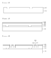
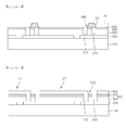
- Figs. 1 to 5 are sectional view for explaining a method for manufacturing a solar battery according to a first embodiment
- Figs. 6 and 7 are sectional view for explaining a method for manufacturing a solar battery according to a modification example of the first embodiment.
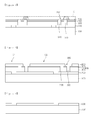
- Figs. 8 to 12 are sectional view for explaining a method for manufacturing a solar battery according to a second embodiment.
- Figs. 13 and 14 are sectional views for explaining a method for manufacturing a solar battery according to a modification example of the second embodiment.
- a substrate, a layer (or film), or an electrode when referred to as being 'on' another substrate, layer, or electrode, it can be directly on the other substrate, layer or electrode, or one or more intervening substrates, layers, or electrodes may also be present. Further, it will be understood that when a substrate, a layer, or an electrode is referred to as being 'under' another substrate, layer, or electrode, it can be directly under the other substrate, layer, or electrode, or one or more intervening substrates, layers, or electrodes may also be present.
- a method for manufacturing a solar battery and a solar battery made by the method will be described in detail according to a first embodiment and a modification example of the first embodiment.
- Figs. 1 to 5 are sectional view for explaining a method for manufacturing a solar battery according to the first embodiment.
- rear electrode patterns 200 are formed on a substrate 100.
- the substrate 100 may be a glass substrate.
- the substrate 100 may be a ceramic substrate such as an alumina substrate, a stainless steel substrate, a titanium substrate, or a polymer substrate.
- a sodalime glass substrate may be used.
- a polymer substrate In case of using a polymer substrate, a polyimide substrate may be used.
- the substrate 100 may be rigid or flexible.
- the rear electrode patterns 200 may be formed by forming a rear electrode layer and patterning the rear electrode layer.
- the rear electrode patterns 200 may be arranged in a stripe or matrix shape corresponding to cells.
- the shape of the rear electrode pattern 200s is not limited to the above-mentioned shapes.
- the rear electrode patterns 200 may have various shapes.
- the rear electrode patterns 200 may be formed of a conductive material such as a metal.
- the rear electrode patterns 200 may be formed through a sputtering process using molybdenum (Mo) as a target.
- Mo molybdenum
- the rear electrode patterns 200 may make ohmic contacts with a light absorption layer and be stable even at a high temperature under a selenium (Se) atmosphere.
- the rear electrode patterns 200 may be constituted by at least one layer.
- the layers may be formed of different materials.
- a light absorption layer 300, a first buffer layer 400, and a second buffer layer 500 are formed on the rear electrode patterns 200.
- the light absorption layer 300 may be formed of a group Ib-IIIb-VIb compound.
- the light absorption layer 300 may include a Cu(In, Ga)Se 2 (CIGS) compound.
- the light absorption layer 300 may include a CuInSe 2 (CIS) compound or CuGaSe 2 (CGS) compound.
- CIS CuInSe 2
- CGS CuGaSe 2
- a CIG metal precursor layer is formed on the rear electrode patterns 200 by using a copper target, an indium target, and a gallium target so as to form the light absorption layer 300.
- the metal precursor layer reacts with selenium (Se) in a selenization process, thereby forming a CIGS light absorption layer 300.
- Se selenium
- an alkali component included in the substrate 100 diffuses to the metal precursor layer and the light absorption layer 300 through the rear electrode patterns 200.
- the alkali component may increase grain sizes of the light absorption layer 300 and improve crystalline properties of the light absorption layer 300.
- the light absorption layer 300 may be formed by a co-evaporation method using copper (Cu), indium (In), gallium (Ga), and selenium (Se).
- the light absorption layer 300 receives light and converts the light into electrical energy.
- the light absorption layer 300 generates a photoelectromotive force by the photovoltaic effect.
- the first buffer layer 400 may be formed by depositing cadmium sulfide (CdS) on the light absorption layer 300.
- CdS cadmium sulfide
- the first buffer layer 400 is an n-type semiconductor layer, and the light absorption layer 300 is a p-type semiconductor layer. Therefore, the light absorption layer 300 and the first buffer layer 400 form a pn junction.
- the second buffer layer 500 may be a transparent electrode layer including one of ITO, ZnO, and i-ZnO.
- the first buffer layer 400 and the second buffer layer 500 are formed between the light absorption layer 300 and a front electrode to be formed later.
- the first buffer layer 400 and the second buffer layer 500 having medium band gaps are interposed for a good junction.
- two buffer layers are formed on the light absorption layer 300.
- the current embodiment is not limited thereto.
- only one buffer layer may be formed.
- a contact pattern 310 and a separation pattern 320 are formed through the light absorption layer 300, the first buffer layer 400, and the second buffer layer 500.
- the contact pattern 310 and the separation pattern 320 may be formed by using a mechanical method or irradiating a laser beam, and the rear electrode patterns 200 may be partially exposed through the contact pattern 310 and the separation pattern 320.
- the contact pattern 310 and the separation pattern 320 may be formed sequentially or simultaneously.
- the light absorption layer 300, the first buffer layer 400, and the second buffer layer 500 form a dummy layer 800 between the contact pattern 310 and the separation pattern 320.
- a mask 10 is disposed on the second buffer layer 500.
- the mask 10 covers the dummy layer 800 and the separation pattern 320 but does not cover the other region.
- a side surface 20 of the mask 10 may be sloped in a manner such that the side surface 20 becomes wider as it goes downward.
- deposition of the front electrode on the second buffer layer 500 may not be affected by a substance deposited on the mask 10.
- the contact pattern 310 may be partially blocked by a part of the front electrode deposited on the mask 10, and thus the front electrode may not be deposited in the contact pattern 310. In this case, the front electrode may not make contact with the rear electrode patterns 200.
- a transparent conductive front electrode 600 is formed on the substrate 100 by using the mask 10.
- the front electrode 600 is also formed in the contact pattern 310 to form interconnections 700.
- the rear electrode patterns 200 and the front electrode 600 are electrically connected through the interconnections 700.
- first and second cells C1 and C2 can be connected to each other through the interconnections 700.
- the rear electrode pattern 200 of the second cell C2 is connected to the front electrode 600 of the first cell C1 neighboring the second cell C2 through the interconnection 700.
- the front electrode 600 is formed by using the mask 10, the front electrode 600 is not formed on the separation pattern 320 and the dummy layer 800.
- the second buffer layer 500 of the dummy layer 800, and the rear electrode patterns 200 are exposed.
- the upper part of the separation pattern 320 close to the front electrode 600 may be wider than the lower part of the separation pattern 320 close to the rear electrode patterns 200.
- the separation pattern 320 is also formed, and then the front electrode 600 is formed using the mask 10.
- processes can be simplified.
- the front electrode 600 After the front electrode 600 is formed, it is not necessary to partially remove the front electrode 600 to form the separation pattern 320. This prevents defects caused by contaminants generating if the front electrode 600 is partially removed.
- the front electrode 600 is formed on the second buffer layer 500 through a sputtering process using an aluminium doped zinc oxide.
- the front electrode 600 is a window layer forming a pn junction with the light absorption layer 300. Since the front electrode 600 functions as a front transparent electrode of a solar battery, the front electrode 600 is formed of a zinc oxide (ZnO) having high optical transmittance and electric conductivity.
- ZnO zinc oxide
- an electrode having a low resistance can be formed by doping an aluminium doped zinc oxide.
- a zinc oxide thin film may be formed as the front electrode 600 by a radio frequency (RF) sputtering method using a ZnO target, a reactive sputtering method using a Zn target, or an organic metal chemical deposition method.
- RF radio frequency
- the front electrode 600 may have a dual structure formed by depositing an indium thin oxide (ITO) thin film having good electro-optical characteristics on the zinc oxide thin film.
- ITO indium thin oxide
- the solar battery of the first embodiment includes the rear electrode patterns 200, the light absorption layer 300, the first buffer layer 400, the second buffer layer 500, and the front electrode 600.
- the rear electrode patterns 200 are formed on the substrate 100 at a plurality of positions spaced apart from each other, and the light absorption layer 300, the first buffer layer 400, the second buffer layer 500, and the front electrode 600 are disposed on the rear electrode patterns 200.
- the interconnections 700 are parts of the front electrode 600 electrically connected to the rear electrode patterns 200 through the light absorption layer 300, the first buffer layer 400, and the second buffer layer 500.
- the separation pattern 320 is formed through the light absorption layer 300, the first buffer layer 400, the second buffer layer 500, and the front electrode 600.
- the light absorption layer 300, the first buffer layer 400, and the second buffer layer 500 constitute the dummy layer 800 between the interconnections 700 and the contact pattern 310.
- the second buffer layer 500 of the dummy layer 800 and the rear electrode patterns 200 close to the separation pattern 320 may be exposed.
- the dummy layer 800 is formed by the stack of the light absorption layer 300, the first buffer layer 400, and the second buffer layer 500, and the front electrode 600 is not formed on the dummy layer 800. Therefore, the top surface of the dummy layer 800 is lower than the top surface of the front electrode 600. The reason for this is that the front electrode 600 is formed after forming the contact pattern 310 and the separation pattern 320 and covering the separation pattern 320 with the mask 10.
- the mask 10 is disposed to cover the dummy layer 800 entirely and the separation pattern 320.
- the embodiment is not limited thereto. It is sufficient that the mask 10 covers the separation pattern 320, and the dummy layer 800 may be partially covered by the mask 10 as shown in Fig. 6 .
- the front electrode 600 covers the dummy layer 800 partially. Like the former case, the top surface of the dummy layer 800 is still lower than the top surface of the front electrode 600.
- Figs. 8 to 12 are sectional view for explaining a method for manufacturing a solar battery according to the
- rear electrode patterns 200 are formed on a substrate 100.
- the substrate 100 may be a glass substrate.
- the substrate 100 may be a ceramic substrate such as an alumina substrate, a stainless steel substrate, a titanium substrate, or a polymer substrate.
- a sodalime glass substrate may be used.
- a polymer substrate In case of using a polymer substrate, a polyimide substrate may be used.
- the substrate 100 may be rigid or flexible.
- the rear electrode patterns 200 may be formed by forming a rear electrode layer and patterning the rear electrode layer.
- the rear electrode patterns 200 may have a stripe or matrix shape corresponding to cells.
- the shape of the rear electrode patterns 200 is not limited to the above-mentioned shapes.
- the rear electrode patterns 200 may have various shapes.
- the rear electrode patterns 200 may be formed of a conductive material such as a metal.
- the rear electrode patterns 200 may be formed through a sputtering process using molybdenum (Mo) as a target.
- Mo molybdenum
- the rear electrode patterns 200 may make ohmic contact with a light absorption layer and be stable at a high temperature under a selenium (Se) atmosphere.
- the rear electrode patterns 200 may be constituted by at least one layer.
- the layers may be formed of different materials.
- a light absorption layer 300 and a first buffer layer 400 are formed on the rear electrode patterns 200.
- the light absorption layer 300 may be formed of a group Ib-IIIb-VIb compound.
- the light absorption layer 300 may include a Cu(In, Ga)Se 2 (CIGS) compound.
- the light absorption layer 300 may include a CuInSe 2 (CIS) compound or CuGaSe 2 (CGS) compound.
- CIS CuInSe 2
- CGS CuGaSe 2
- a CIG metal precursor layer is formed on the rear electrode patterns 200 by using a copper target, an indium target, and a gallium target so as to form the light absorption layer 300.
- the metal precursor layer reacts with selenium (Se) in a selenization process to form a CIGS light absorption layer 300.
- Se selenium
- an alkali component included in the substrate 100 diffuses to the metal precursor layer and the light absorption layer 300 through the rear electrode patterns 200.
- the alkali component may increase grain sizes of the light absorption layer 300 and improve crystalline properties of the light absorption layer 300.
- the light absorption layer 300 may be formed by a co-evaporation method using copper (Cu), indium (In), gallium (Ga), and selenium (Se).
- the light absorption layer 300 receives light and converts the light into electrical energy.
- the light absorption layer 300 generates a photoelectromotive force by the photovoltaic effect.
- the first buffer layer 400 may be formed by depositing cadmium sulfide (CdS) on the light absorption layer 300.
- CdS cadmium sulfide
- the first buffer layer 400 is an n-type semiconductor layer, and the light absorption layer 300 is a p-type semiconductor layer. Therefore, the light absorption layer 300 and the first buffer layer 400 forms a pn junction.
- a contact pattern 310 and a separation pattern 320 are formed through the light absorption layer 300 and the first buffer layer 400.
- the contact pattern 310 and the separation pattern 320 may be formed by using a mechanical method or irradiating a laser beam, and the rear electrode patterns 200 are partially exposed through the contact pattern 310 and the separation pattern 320.
- the contact pattern 310 and the separation pattern 320 may be formed sequentially or simultaneously.
- the light absorption layer 300, the first buffer layer 400, and the second buffer layer 500 form a dummy layer 900 between the contact pattern 310 and the separation pattern 320.
- a mask 10 is disposed on the second buffer layer 500.
- the mask 10 covers the dummy layer 900 and the separation pattern 320 but does not cover the other region.
- a side 20 of the mask 10 may be sloped in a manner such that the side 20 becomes wider as it goes downward.
- deposition of the front electrode on the first buffer layer 400 may not be affected by a substance deposited on the mask 10.
- the contact pattern 310 may be partially blocked by a part of the front electrode deposited on the mask 10, and thus the front electrode may not be deposited in the contact pattern 310. In this case, the front electrode may not make contact with the rear electrode patterns 200.
- a second buffer layer 500 and a transparent conductive front electrode 600 are formed on the substrate 100 by using the mask 10.
- the second buffer layer 500 may be a transparent electrode layer including one of ITO, ZnO, and i-ZnO.
- the first buffer layer 400 and the second buffer layer 500 are disposed between the light absorption layer 300 and the front electrode 600.
- the first buffer layer 400 and the second buffer layer 500 having medium band gaps are interposed for a good junction.
- two buffer layers are formed on the light absorption layer 300.
- the current embodiment is not limited thereto.
- only one buffer layer may be formed.
- the second buffer layer 500 and the front electrode 600 are stacked on the first buffer layer 400, the second buffer layer 500 and the front electrode 600 are also formed in the contact pattern 310 to form interconnections 700.
- the second buffer layer 500 is formed on the bottom and side surfaces of the contact pattern 310, and then the front electrode 600 is formed in the contact pattern 310 to form the interconnections 700.
- the second buffer layer 500 is disposed between the front electrode 600 and the rear electrode patterns 200.
- the front electrode 600 is formed on the second buffer layer 500 through a sputtering process using a zinc oxide doped with aluminium.
- the front electrode 600 is a window layer forming a pn junction with the light absorption layer 300. Since the front electrode 600 functions as a front transparent electrode of a solar battery, the front electrode 600 is formed of a zinc oxide (ZnO) having high optical transmittance and electric conductivity.
- ZnO zinc oxide
- an electrode having a low resistance can be formed by doping a zinc oxide with aluminium.
- a zinc oxide thin film may be formed as the front electrode 600 by a radio frequency (RF) sputtering method using a ZnO target, a reactive sputtering method using a Zn target, or an organic metal chemical deposition method.
- RF radio frequency
- the front electrode 600 may have a dual structure formed by depositing an indium thin oxide (ITO) thin film having good electro-optical characteristics on the zinc oxide thin film.
- ITO indium thin oxide
- the aluminium included in the front electrode 600 may diffuse to the second buffer layer 500.
- the rear electrode patterns 200 and the front electrode 600 are electrically connected through the interconnections 700.
- first and second cells C1 and C2 can be connected to each other through the interconnections 700.
- the rear electrode pattern 200 of the second cell C2 is connected to the front electrode 600 of the first cell C1 neighboring the second cell C2 through the interconnection 700.
- the second buffer layer 500 and the front electrode 600 are formed by using the mask 10, the second buffer layer 500 and the front electrode 600 are not formed on the separation pattern 320 and the dummy layer 900.
- the first buffer layer 400 of the dummy layer 900 and the rear electrode pattern 200 are exposed.
- the upper part of the separation pattern 320 close to the second buffer layer 500 and the front electrode 600 may be wider than the lower part of the separation pattern 320 close to the rear electrode pattern 200.
- the front electrode 600 after the front electrode 600 is formed, the dummy layer 900 and the separation pattern 320 are exposed.
- the current embodiment is not limited thereto.
- the front electrode 600 may be formed on a part of the first buffer layer 400 of the dummy layer 900 by modifying the mask 10.
- the first buffer layer 400 of the dummy layer 900 may be partially exposed.
- the separation pattern 320 is also formed, and then the second buffer layer 500 and the front electrode 600 are formed using the mask 10.
- processes can be simplified.
- the front electrode 600 After the front electrode 600 is formed, it is not necessary to partially remove the front electrode 600 to form the separation pattern 320. This prevents defects caused by contaminants generating if the front electrode 600 is partially removed.
- the solar battery of the second embodiment includes the rear electrode pattern 200, the light absorption layer 300, the first buffer layer 400, the second buffer layer 500, and the front electrode 600.
- the rear electrode patterns 200 are formed on the substrate 100 at a plurality of positions spaced apart from each other, and the light absorption layer 300, the first buffer layer 400, the second buffer layer 500, and the front electrode 600 are disposed on the rear electrode patterns 200.
- the interconnections 700 are parts of the front electrode 600 electrically connected to the rear electrode patterns 200 through the light absorption layer 300 and the first buffer layer 400.
- the separation pattern 320 is formed through the light absorption layer 300, the first buffer layer 400, the second buffer layer 500, and the front electrode 600.
- the light absorption layer 300 and the first buffer layer 400 form the dummy layer 900 between the interconnections 700 and the contact pattern 310.
- the first buffer layer 400 of the dummy layer 900 and the rear electrode patterns 200 close to the separation pattern 320 may be exposed.
- the interconnections 700 are formed by stacks of the second buffer layer 500 and the front electrode 600.
- the dummy layer 900 is formed by the stack of the light absorption layer 300 and the first buffer layer 400, and the front electrode 600 is not formed on the dummy layer 900. Therefore, the top surface of the dummy layer 900 is lower than the top surface of the front electrode 600. The reason for this is that the front electrode 600 is formed after forming the contact pattern 310 and the separation pattern 320 and covering the separation pattern 320 with the mask 10.
- the mask 10 is disposed to cover the dummy layer 900 entirely and the separation pattern 320.
- the embodiment is not limited thereto. It is sufficient that the mask 10 covers the separation pattern 320, and the dummy layer 900 may be partially covered by the mask 10 as shown in Fig. 13 .
- the front electrode 600 covers the dummy layer 900 partially. Like the former case, the top surface of the dummy layer 900 is still lower than the top surface of the front electrode 600.
- the front electrode is formed using the mask. Therefore, processes can be simplified.
- the front electrode After the front electrode is formed, it is not necessary to partially remove the front electrode to form the separation pattern. This prevents defects caused by contaminants generating if the front electrode is partially removed.
Landscapes
- Photovoltaic Devices (AREA)
Abstract
Description
- The present disclosure relates to a solar battery and a method for manufacturing the solar battery.
- As the consumption of energy increases, research has been conducted on solar batteries for converting solar energy into electric energy.
- Particularly, Cu(In,Ga)Se2 (CIGS) solar batteries are widely used, which are a pn hetero junction devices having a substrate structure including a glass substrate, a metal rear electrode layer, a p-type CIGS light absorption layer, a high resistance buffer layer, and an n-type window layer.
- In such a solar battery, cells are defined by a separation pattern formed by etching a light absorption layer, a buffer layer, and a front electrode (an n-type window layer). However, due to particles generating during a process of forming the separation pattern, cells may become defective, and thus the solar battery may malfunction.
- Embodiments provide a solar battery and a method for manufacturing the solar batter, so that solar battery manufacturing processes can be simplified and particles can be reduced during the processes so as to minimize defects.
- In an embodiment, a solar battery includes: a plurality of rear electrode patterns disposed on a substrate and spaced apart from each other; a light absorption layer on the rear electrode patterns; a front electrode on the light absorption layer; an interconnection which is a part of the front electrode penetrating the light absorption layer and electrically connected to the rear electrode patterns; a separation pattern penetrating the light absorption layer and the front electrode for defining unit cells; and a dummy layer between the interconnection and the separation pattern. The dummy layer may have a top surface lower than that of the front electrode.
- In another embodiment, a solar battery includes: a plurality of rear electrode patterns disposed on a substrate and spaced apart from each other; a light absorption layer, a first buffer layer, and a second buffer layer on the rear electrode patterns; a front electrode on the second buffer layer; an interconnection which is parts of the second buffer layer and the front electrode penetrating the light absorption layer and the first buffer layer and electrically connected to the rear electrode patterns; and a separation pattern penetrating the light absorption layer, the first buffer layer, the second buffer layer, and the front electrode for defining unit cells. The interconnection may be formed by a stack of the second buffer layer and the front electrode.
- In another embodiment, there is provided a method for manufacturing a solar battery, the method includes: forming a plurality of rear electrode patterns spaced apart from each other on a substrate; forming a light absorption layer and a first buffer layer on the substrate where the rear electrode patterns are formed; forming a contact pattern and a separation pattern that penetrate the light absorption layer and the first buffer layer; and forming a front electrode on a front side of the substrate by using a mask covering a dummy layer and the seperation pattern, the dummy layer comprising parts of the light absorption layer and the first buffer layer disposed between the contact pattern and the separation pattern. After the front electrode is formed, the dummy layer and the rear electrode patterns close to the separation pattern are exposed.
- According to the solar cell and the solar cell manufacturing method of the embodiments, after forming the light absorption layer, the buffer layer, the contact pattern, and the separation pattern, the front electrode is formed using the mask. Therefore, processes can be simplified.
- In addition, after the front electrode is formed, it is not necessary to partially remove the front electrode to form the separation pattern. This prevents defects caused by contaminants generating if the front electrode is partially removed.
-
Figs. 1 to 5 are sectional view for explaining a method for manufacturing a solar battery according to a first embodiment -
Figs. 6 and 7 are sectional view for explaining a method for manufacturing a solar battery according to a modification example of the first embodiment. -
Figs. 8 to 12 are sectional view for explaining a method for manufacturing a solar battery according to a second embodiment. -
Figs. 13 and14 are sectional views for explaining a method for manufacturing a solar battery according to a modification example of the second embodiment. - In the following description, it will be understood that when a substrate, a layer (or film), or an electrode is referred to as being 'on' another substrate, layer, or electrode, it can be directly on the other substrate, layer or electrode, or one or more intervening substrates, layers, or electrodes may also be present. Further, it will be understood that when a substrate, a layer, or an electrode is referred to as being 'under' another substrate, layer, or electrode, it can be directly under the other substrate, layer, or electrode, or one or more intervening substrates, layers, or electrodes may also be present. In addition, it will also be understood that when a layer is referred to as being 'between' two layers, it can be the only layer between the two layers, or one or more intervening layers may also be present. Further, the reference about 'on' and 'under' each layer will be made on the basis of drawings. Also, in the drawings, the sizes of elements may be exaggerated for clarity of illustration, and the size of each element does not entirely reflect an actual size.
- With reference to
Figs. 1 to 7 , a method for manufacturing a solar battery and a solar battery made by the method will be described in detail according to a first embodiment and a modification example of the first embodiment. -
Figs. 1 to 5 are sectional view for explaining a method for manufacturing a solar battery according to the first embodiment. - First, as shown in
Fig. 1 ,rear electrode patterns 200 are formed on asubstrate 100. - The
substrate 100 may be a glass substrate. Alternatively, thesubstrate 100 may be a ceramic substrate such as an alumina substrate, a stainless steel substrate, a titanium substrate, or a polymer substrate. - In case of using a glass substrate, a sodalime glass substrate may be used. In case of using a polymer substrate, a polyimide substrate may be used.
- In addition, the
substrate 100 may be rigid or flexible. - The
rear electrode patterns 200 may be formed by forming a rear electrode layer and patterning the rear electrode layer. - In addition, the
rear electrode patterns 200 may be arranged in a stripe or matrix shape corresponding to cells. - However, the shape of the rear electrode pattern 200s is not limited to the above-mentioned shapes. The
rear electrode patterns 200 may have various shapes. - The
rear electrode patterns 200 may be formed of a conductive material such as a metal. - For example, the
rear electrode patterns 200 may be formed through a sputtering process using molybdenum (Mo) as a target. - In this case, owing to high electric conductivity of molybdenum (Mo), the
rear electrode patterns 200 may make ohmic contacts with a light absorption layer and be stable even at a high temperature under a selenium (Se) atmosphere. - Although not shown in the drawings, the
rear electrode patterns 200 may be constituted by at least one layer. - In the case where the
rear electrode patterns 200 are constituted by a plurality of layers, the layers may be formed of different materials. - Next, as shown in
Fig. 2 , alight absorption layer 300, afirst buffer layer 400, and asecond buffer layer 500 are formed on therear electrode patterns 200. - The
light absorption layer 300 may be formed of a group Ib-IIIb-VIb compound. - For example, the
light absorption layer 300 may include a Cu(In, Ga)Se2 (CIGS) compound. - Alternatively, the
light absorption layer 300 may include a CuInSe2 (CIS) compound or CuGaSe2 (CGS) compound. - For example, a CIG metal precursor layer is formed on the
rear electrode patterns 200 by using a copper target, an indium target, and a gallium target so as to form thelight absorption layer 300. - Then, the metal precursor layer reacts with selenium (Se) in a selenization process, thereby forming a CIGS
light absorption layer 300. - In addition, during the metal precursor forming process and the selenization process, an alkali component included in the
substrate 100 diffuses to the metal precursor layer and thelight absorption layer 300 through therear electrode patterns 200. - The alkali component may increase grain sizes of the
light absorption layer 300 and improve crystalline properties of thelight absorption layer 300. - Alternatively, the
light absorption layer 300 may be formed by a co-evaporation method using copper (Cu), indium (In), gallium (Ga), and selenium (Se). - The
light absorption layer 300 receives light and converts the light into electrical energy. Thelight absorption layer 300 generates a photoelectromotive force by the photovoltaic effect. - The
first buffer layer 400 may be formed by depositing cadmium sulfide (CdS) on thelight absorption layer 300. - At this time, the
first buffer layer 400 is an n-type semiconductor layer, and thelight absorption layer 300 is a p-type semiconductor layer. Therefore, thelight absorption layer 300 and thefirst buffer layer 400 form a pn junction. - The
second buffer layer 500 may be a transparent electrode layer including one of ITO, ZnO, and i-ZnO. - The
first buffer layer 400 and thesecond buffer layer 500 are formed between thelight absorption layer 300 and a front electrode to be formed later. - That is, since the
light absorption layer 300 and the front electrode are largely different in lattice constant and energy band gap, thefirst buffer layer 400 and thesecond buffer layer 500 having medium band gaps are interposed for a good junction. - In the current embodiment, two buffer layers are formed on the
light absorption layer 300. However, the current embodiment is not limited thereto. For example, only one buffer layer may be formed. - Next, as shown in
Fig. 3 , acontact pattern 310 and aseparation pattern 320 are formed through thelight absorption layer 300, thefirst buffer layer 400, and thesecond buffer layer 500. - The
contact pattern 310 and theseparation pattern 320 may be formed by using a mechanical method or irradiating a laser beam, and therear electrode patterns 200 may be partially exposed through thecontact pattern 310 and theseparation pattern 320. - The
contact pattern 310 and theseparation pattern 320 may be formed sequentially or simultaneously. - At this time, the
light absorption layer 300, thefirst buffer layer 400, and thesecond buffer layer 500 form adummy layer 800 between thecontact pattern 310 and theseparation pattern 320. - Next, as shown in
Fig. 4 , amask 10 is disposed on thesecond buffer layer 500. - The
mask 10 covers thedummy layer 800 and theseparation pattern 320 but does not cover the other region. - A
side surface 20 of themask 10 may be sloped in a manner such that theside surface 20 becomes wider as it goes downward. - In this case, when a front electrode is formed in a later process, deposition of the front electrode on the
second buffer layer 500 may not be affected by a substance deposited on themask 10. - That is, if the
side surface 20 of themask 10 is not sloped, thecontact pattern 310 may be partially blocked by a part of the front electrode deposited on themask 10, and thus the front electrode may not be deposited in thecontact pattern 310. In this case, the front electrode may not make contact with therear electrode patterns 200. - Next, as shown in
Fig. 5 , a transparent conductivefront electrode 600 is formed on thesubstrate 100 by using themask 10. - When the transparent conductive
front electrode 600 is formed on thesecond buffer layer 500, thefront electrode 600 is also formed in thecontact pattern 310 to forminterconnections 700. - The
rear electrode patterns 200 and thefront electrode 600 are electrically connected through theinterconnections 700. - For example, first and second cells C1 and C2 can be connected to each other through the
interconnections 700. For example, therear electrode pattern 200 of the second cell C2 is connected to thefront electrode 600 of the first cell C1 neighboring the second cell C2 through theinterconnection 700. - At this time, since the
front electrode 600 is formed by using themask 10, thefront electrode 600 is not formed on theseparation pattern 320 and thedummy layer 800. - That is, after the
front electrode 600 is formed, thesecond buffer layer 500 of thedummy layer 800, and therear electrode patterns 200 are exposed. - In addition, since the
front electrode 600 is not formed on thedummy layer 800, the upper part of theseparation pattern 320 close to thefront electrode 600 may be wider than the lower part of theseparation pattern 320 close to therear electrode patterns 200. - In the current embodiment, when the
contact pattern 310 is formed, theseparation pattern 320 is also formed, and then thefront electrode 600 is formed using themask 10. Thus, processes can be simplified. - In addition, after the
front electrode 600 is formed, it is not necessary to partially remove thefront electrode 600 to form theseparation pattern 320. This prevents defects caused by contaminants generating if thefront electrode 600 is partially removed. - The
front electrode 600 is formed on thesecond buffer layer 500 through a sputtering process using an aluminium doped zinc oxide. - The
front electrode 600 is a window layer forming a pn junction with thelight absorption layer 300. Since thefront electrode 600 functions as a front transparent electrode of a solar battery, thefront electrode 600 is formed of a zinc oxide (ZnO) having high optical transmittance and electric conductivity. - At this time, an electrode having a low resistance can be formed by doping an aluminium doped zinc oxide.
- A zinc oxide thin film may be formed as the
front electrode 600 by a radio frequency (RF) sputtering method using a ZnO target, a reactive sputtering method using a Zn target, or an organic metal chemical deposition method. - In addition, the
front electrode 600 may have a dual structure formed by depositing an indium thin oxide (ITO) thin film having good electro-optical characteristics on the zinc oxide thin film. - With reference to
Fig. 5 , a detailed explanation will be given on the solar battery formed by the above-described solar battery manufacturing method of the first embodiment. - As shown in
Fig. 5 , the solar battery of the first embodiment includes therear electrode patterns 200, thelight absorption layer 300, thefirst buffer layer 400, thesecond buffer layer 500, and thefront electrode 600. - The
rear electrode patterns 200 are formed on thesubstrate 100 at a plurality of positions spaced apart from each other, and thelight absorption layer 300, thefirst buffer layer 400, thesecond buffer layer 500, and thefront electrode 600 are disposed on therear electrode patterns 200. - The
interconnections 700 are parts of thefront electrode 600 electrically connected to therear electrode patterns 200 through thelight absorption layer 300, thefirst buffer layer 400, and thesecond buffer layer 500. - The
separation pattern 320 is formed through thelight absorption layer 300, thefirst buffer layer 400, thesecond buffer layer 500, and thefront electrode 600. - The
light absorption layer 300, thefirst buffer layer 400, and thesecond buffer layer 500 constitute thedummy layer 800 between theinterconnections 700 and thecontact pattern 310. - The
second buffer layer 500 of thedummy layer 800 and therear electrode patterns 200 close to theseparation pattern 320 may be exposed. - In this way, the
dummy layer 800 is formed by the stack of thelight absorption layer 300, thefirst buffer layer 400, and thesecond buffer layer 500, and thefront electrode 600 is not formed on thedummy layer 800. Therefore, the top surface of thedummy layer 800 is lower than the top surface of thefront electrode 600. The reason for this is that thefront electrode 600 is formed after forming thecontact pattern 310 and theseparation pattern 320 and covering theseparation pattern 320 with themask 10. - In the above-described embodiment, the
mask 10 is disposed to cover thedummy layer 800 entirely and theseparation pattern 320. However, the embodiment is not limited thereto. It is sufficient that themask 10 covers theseparation pattern 320, and thedummy layer 800 may be partially covered by themask 10 as shown inFig. 6 . In this case, as shown inFig. 7 , thefront electrode 600 covers thedummy layer 800 partially. Like the former case, the top surface of thedummy layer 800 is still lower than the top surface of thefront electrode 600. - With reference to
Figs. 8 to 14 , a method for manufacturing a solar battery and a solar battery made by the method will be described in detail according to a second embodiment and a modification example of the second embodiment. -
Figs. 8 to 12 are sectional view for explaining a method for manufacturing a solar battery according to the - First, as shown in
Fig. 8 ,rear electrode patterns 200 are formed on asubstrate 100. - The
substrate 100 may be a glass substrate. Alternatively, thesubstrate 100 may be a ceramic substrate such as an alumina substrate, a stainless steel substrate, a titanium substrate, or a polymer substrate. - In case of using a glass substrate, a sodalime glass substrate may be used. In case of using a polymer substrate, a polyimide substrate may be used.
- In addition, the
substrate 100 may be rigid or flexible. - The
rear electrode patterns 200 may be formed by forming a rear electrode layer and patterning the rear electrode layer. - In addition, the
rear electrode patterns 200 may have a stripe or matrix shape corresponding to cells. - However, the shape of the
rear electrode patterns 200 is not limited to the above-mentioned shapes. Therear electrode patterns 200 may have various shapes. - The
rear electrode patterns 200 may be formed of a conductive material such as a metal. - For example, the
rear electrode patterns 200 may be formed through a sputtering process using molybdenum (Mo) as a target. - In this case, owing to high electric conductivity of molybdenum (Mo), the
rear electrode patterns 200 may make ohmic contact with a light absorption layer and be stable at a high temperature under a selenium (Se) atmosphere. - Although not shown in the drawings, the
rear electrode patterns 200 may be constituted by at least one layer. - In the case where the
rear electrode patterns 200 are constituted by a plurality of layers, the layers may be formed of different materials. - Next, as shown in
Fig. 9 , alight absorption layer 300 and afirst buffer layer 400 are formed on therear electrode patterns 200. - The
light absorption layer 300 may be formed of a group Ib-IIIb-VIb compound. - For example, the
light absorption layer 300 may include a Cu(In, Ga)Se2 (CIGS) compound. - Alternatively, the
light absorption layer 300 may include a CuInSe2 (CIS) compound or CuGaSe2 (CGS) compound. - For example, a CIG metal precursor layer is formed on the
rear electrode patterns 200 by using a copper target, an indium target, and a gallium target so as to form thelight absorption layer 300. - Then, the metal precursor layer reacts with selenium (Se) in a selenization process to form a CIGS
light absorption layer 300. - In addition, during the metal precursor forming process and the selenization process, an alkali component included in the
substrate 100 diffuses to the metal precursor layer and thelight absorption layer 300 through therear electrode patterns 200. - The alkali component may increase grain sizes of the
light absorption layer 300 and improve crystalline properties of thelight absorption layer 300. - Alternatively, the
light absorption layer 300 may be formed by a co-evaporation method using copper (Cu), indium (In), gallium (Ga), and selenium (Se). - The
light absorption layer 300 receives light and converts the light into electrical energy. Thelight absorption layer 300 generates a photoelectromotive force by the photovoltaic effect. - The
first buffer layer 400 may be formed by depositing cadmium sulfide (CdS) on thelight absorption layer 300. - At this time, the
first buffer layer 400 is an n-type semiconductor layer, and thelight absorption layer 300 is a p-type semiconductor layer. Therefore, thelight absorption layer 300 and thefirst buffer layer 400 forms a pn junction. - Next, as shown in
Fig. 10 , acontact pattern 310 and aseparation pattern 320 are formed through thelight absorption layer 300 and thefirst buffer layer 400. - The
contact pattern 310 and theseparation pattern 320 may be formed by using a mechanical method or irradiating a laser beam, and therear electrode patterns 200 are partially exposed through thecontact pattern 310 and theseparation pattern 320. - The
contact pattern 310 and theseparation pattern 320 may be formed sequentially or simultaneously. - At this time, the
light absorption layer 300, thefirst buffer layer 400, and thesecond buffer layer 500 form adummy layer 900 between thecontact pattern 310 and theseparation pattern 320. - Next, as shown in
Fig. 11 , amask 10 is disposed on thesecond buffer layer 500. - The
mask 10 covers thedummy layer 900 and theseparation pattern 320 but does not cover the other region. - A
side 20 of themask 10 may be sloped in a manner such that theside 20 becomes wider as it goes downward. - In this case, when a front electrode is formed in a later process, deposition of the front electrode on the
first buffer layer 400 may not be affected by a substance deposited on themask 10. - That is, if the
side surface 20 of themask 10 is not sloped, thecontact pattern 310 may be partially blocked by a part of the front electrode deposited on themask 10, and thus the front electrode may not be deposited in thecontact pattern 310. In this case, the front electrode may not make contact with therear electrode patterns 200. - Next, as shown in
Fig. 12 , asecond buffer layer 500 and a transparent conductivefront electrode 600 are formed on thesubstrate 100 by using themask 10. - The
second buffer layer 500 may be a transparent electrode layer including one of ITO, ZnO, and i-ZnO. - The
first buffer layer 400 and thesecond buffer layer 500 are disposed between thelight absorption layer 300 and thefront electrode 600. - That is, since the
light absorption layer 300 and the front electrode are largely different in lattice constant and energy band gap, thefirst buffer layer 400 and thesecond buffer layer 500 having medium band gaps are interposed for a good junction. - In the current embodiment, two buffer layers are formed on the
light absorption layer 300. However, the current embodiment is not limited thereto. For example, only one buffer layer may be formed. - When the
second buffer layer 500 and thefront electrode 600 are stacked on thefirst buffer layer 400, thesecond buffer layer 500 and thefront electrode 600 are also formed in thecontact pattern 310 to forminterconnections 700. - That is, the
second buffer layer 500 is formed on the bottom and side surfaces of thecontact pattern 310, and then thefront electrode 600 is formed in thecontact pattern 310 to form theinterconnections 700. - At this time, the
second buffer layer 500 is disposed between thefront electrode 600 and therear electrode patterns 200. - The
front electrode 600 is formed on thesecond buffer layer 500 through a sputtering process using a zinc oxide doped with aluminium. - The
front electrode 600 is a window layer forming a pn junction with thelight absorption layer 300. Since thefront electrode 600 functions as a front transparent electrode of a solar battery, thefront electrode 600 is formed of a zinc oxide (ZnO) having high optical transmittance and electric conductivity. - At this time, an electrode having a low resistance can be formed by doping a zinc oxide with aluminium.
- A zinc oxide thin film may be formed as the
front electrode 600 by a radio frequency (RF) sputtering method using a ZnO target, a reactive sputtering method using a Zn target, or an organic metal chemical deposition method. - In addition, the
front electrode 600 may have a dual structure formed by depositing an indium thin oxide (ITO) thin film having good electro-optical characteristics on the zinc oxide thin film. - In the later processes, the aluminium included in the
front electrode 600 may diffuse to thesecond buffer layer 500. - The
rear electrode patterns 200 and thefront electrode 600 are electrically connected through theinterconnections 700. - For example, first and second cells C1 and C2 can be connected to each other through the
interconnections 700. For example, therear electrode pattern 200 of the second cell C2 is connected to thefront electrode 600 of the first cell C1 neighboring the second cell C2 through theinterconnection 700. - At this time, since the
second buffer layer 500 and thefront electrode 600 are formed by using themask 10, thesecond buffer layer 500 and thefront electrode 600 are not formed on theseparation pattern 320 and thedummy layer 900. - That is, after the
second buffer layer 500 and thefront electrode 600 are formed, thefirst buffer layer 400 of thedummy layer 900 and therear electrode pattern 200 are exposed. - In addition, since the
second buffer layer 500 and thefront electrode 600 are not formed on thedummy layer 900, the upper part of theseparation pattern 320 close to thesecond buffer layer 500 and thefront electrode 600 may be wider than the lower part of theseparation pattern 320 close to therear electrode pattern 200. - In the current embodiment, after the
front electrode 600 is formed, thedummy layer 900 and theseparation pattern 320 are exposed. However, the current embodiment is not limited thereto. For example, thefront electrode 600 may be formed on a part of thefirst buffer layer 400 of thedummy layer 900 by modifying themask 10. - That is, the
first buffer layer 400 of thedummy layer 900 may be partially exposed. - In the current embodiment, when the
contact pattern 310 is formed, theseparation pattern 320 is also formed, and then thesecond buffer layer 500 and thefront electrode 600 are formed using themask 10. Thus, processes can be simplified. - In addition, after the
front electrode 600 is formed, it is not necessary to partially remove thefront electrode 600 to form theseparation pattern 320. This prevents defects caused by contaminants generating if thefront electrode 600 is partially removed. - With reference to
Fig. 12 , a detailed explanation will be given on the solar battery formed by the above-described solar battery manufacturing method of the second embodiment. - As shown in
Fig. 12 , the solar battery of the second embodiment includes therear electrode pattern 200, thelight absorption layer 300, thefirst buffer layer 400, thesecond buffer layer 500, and thefront electrode 600. - The
rear electrode patterns 200 are formed on thesubstrate 100 at a plurality of positions spaced apart from each other, and thelight absorption layer 300, thefirst buffer layer 400, thesecond buffer layer 500, and thefront electrode 600 are disposed on therear electrode patterns 200. - The
interconnections 700 are parts of thefront electrode 600 electrically connected to therear electrode patterns 200 through thelight absorption layer 300 and thefirst buffer layer 400. - The
separation pattern 320 is formed through thelight absorption layer 300, thefirst buffer layer 400, thesecond buffer layer 500, and thefront electrode 600. - The
light absorption layer 300 and thefirst buffer layer 400 form thedummy layer 900 between theinterconnections 700 and thecontact pattern 310. - The
first buffer layer 400 of thedummy layer 900 and therear electrode patterns 200 close to theseparation pattern 320 may be exposed. - The
interconnections 700 are formed by stacks of thesecond buffer layer 500 and thefront electrode 600. - The
dummy layer 900 is formed by the stack of thelight absorption layer 300 and thefirst buffer layer 400, and thefront electrode 600 is not formed on thedummy layer 900. Therefore, the top surface of thedummy layer 900 is lower than the top surface of thefront electrode 600. The reason for this is that thefront electrode 600 is formed after forming thecontact pattern 310 and theseparation pattern 320 and covering theseparation pattern 320 with themask 10. - In the above-described embodiment, the
mask 10 is disposed to cover thedummy layer 900 entirely and theseparation pattern 320. However, the embodiment is not limited thereto. It is sufficient that themask 10 covers theseparation pattern 320, and thedummy layer 900 may be partially covered by themask 10 as shown inFig. 13 . In this case, as shown inFig. 14 , thefront electrode 600 covers thedummy layer 900 partially. Like the former case, the top surface of thedummy layer 900 is still lower than the top surface of thefront electrode 600. - According to the solar battery and the solar battery manufacturing method of the embodiments, after forming the light absorption layer, the buffer layer, the contact pattern, and the separation pattern, the front electrode is formed using the mask. Therefore, processes can be simplified.
- In addition, after the front electrode is formed, it is not necessary to partially remove the front electrode to form the separation pattern. This prevents defects caused by contaminants generating if the front electrode is partially removed.
- Although embodiments have been described with reference to a number of illustrative embodiments thereof, it should be understood that numerous other modifications and embodiments can be devised by those skilled in the art that will fall within the spirit and scope of the principles of this disclosure. More particularly, various variations and modifications are possible in the component parts and/or arrangements of the subject combination arrangement within the scope of the disclosure, the drawings and the appended claims. In addition to variations and modifications in the component parts and/or arrangements, alternative uses will also be apparent to those skilled in the art.
Claims (20)
- A solar battery comprising:a plurality of rear electrode patterns disposed on a substrate and spaced apart from each other;a light absorption layer on the rear electrode patterns;a front electrode on the light absorption layer;an interconnection which is a part of the front electrode penetrating the light absorption layer and electrically connected to the rear electrode patterns;a separation pattern penetrating the light absorption layer and the front electrode for defining unit cells; anda dummy layer between the interconnection and the separation pattern,wherein the dummy layer has a top surface lower than that of the front electrode.
- The solar battery according to claim 1, further comprising a first buffer layer and a second buffer layer is disposed on the first buffer layer, the first buffer layer and the second buffer layer disposed between the light absorption layer and the front electrode, and
wherein the dummy layer includes a stack of the light absorption layer, the first buffer layer, and the second buffer layer. - The solar battery according to claim 2, wherein the second buffer layer of the dummy layer and the rear electrode patterns close to the separation pattern are exposed.
- The solar battery according to claim 2, wherein the front electrode covers at least a part of the second buffer layer of the dummy layer.
- The solar battery according to claim 1, further comprising a first buffer layer and a second buffer layer is disposed on the first buffer layer, the first buffer layer and the second buffer layer disposed between the light absorption layer and the front electrode, and
wherein the dummy layer includes a stack of the light absorption layer and the second buffer layer. - The solar battery according to claim 5, wherein the first buffer layer of the dummy layer and the rear electrode patterns close to the separation pattern are exposed.
- The solar battery according to claim 5, wherein the second buffer layer and the front electrode cover at least a part of the first buffer layer of the dummy layer.
- The solar battery according to claim 5, wherein the interconnection includes a stack of the second buffer layer and the front electrode.
- The solar battery according to claim 1, wherein an upper part of the separation pattern close to the front electrode is wider than a lower part of the separation pattern close to the rear electrode patterns.
- A solar battery comprising:a plurality of rear electrode patterns disposed on a substrate and spaced apart from each other;a light absorption layer, a first buffer layer, and a second buffer layer on the rear electrode patterns;a front electrode on the second buffer layer;an interconnection which is parts of the second buffer layer and the front electrode penetrating the light absorption layer and the first buffer layer and electrically connected to the rear electrode patterns; anda separation pattern penetrating the light absorption layer, the first buffer layer, the second buffer layer, and the front electrode for defining unit cells;wherein the interconnection includs a stack of the second buffer layer and the front electrode.
- The solar battery according to claim 10, wherein the second buffer layer of the interconnection is disposed between the rear electrode patterns and the front electrode.
- The solar battery according to claim 10, wherein a dummy layer is formed between the interconnection and the separation pattern by a stack of the light absorption layer and the first buffer layer,
wherein the first buffer layer of the dummy layer and the rear electrode patterns close to the separation pattern are exposed. - The solar battery according to claim 10, wherein a dummy layer is formed between the interconnection and the separation pattern by a stack of the light absorption layer and the first buffer layer,
wherein the front electrode covers a part of the first buffer layer of the dummy layer. - A method for manufacturing a solar battery, comprising:forming a plurality of rear electrode patterns spaced apart from each other on a substrate;forming a light absorption layer and a first buffer layer on the substrate where the rear electrode patterns are formed;forming a contact pattern and a separation pattern that penetrate the light absorption layer and the first buffer layer; andforming a front electrode on a front side of the substrate by using a mask covering a dummy layer and the seperation pattern, the dummy layer comprising parts of the light absorption layer and the first buffer layer disposed between the contact pattern and the separation pattern,wherein after the front electrode is formed, the dummy layer and the rear electrode patterns close to the separation pattern are exposed.
- The method according to claim 14, wherein between the forming of the light absorption layer and the first buffer layer and the forming of the contact pattern and the separation pattern, the method further comprising forming a second buffer layer on the first buffer layer,
wherein the contact pattern and the separation pattern penetrate the light absorption layer, the first buffer layer, and the second buffer layer, and
the mask covering the dummy layer and the separation pattern are disposed on the second buffer layer. - The method according to claim 15, wherein the dummy layer includes a stack of the light absorption layer, the first buffer layer, and the second buffer layer.
- The method according to claim 14, wherein in the forming of the front electrode, a second buffer layer is formed by using the mask, and then the front electrode is formed on the second buffer layer.
- The method according to claim 17, wherein the dummy layer includes a stack of the light absorption layer and the first buffer layer.
- The method according to claim 17, wherein when the second buffer layer and the front electrode are formed, the second buffer layer and the front electrode are disposed in the contact pattern to form an interconnection,
the second buffer layer is disposed between the rear electrode patterns and the front electrode. - The method according to claim 19, wherein the front electrode is formed of an aluminium doped zinc oxide (ZnO), and the aluminium diffuses to the second buffer layer.
Applications Claiming Priority (2)
| Application Number | Priority Date | Filing Date | Title |
|---|---|---|---|
| KR1020090059517A KR101028310B1 (en) | 2009-06-30 | 2009-06-30 | Solar cell and manufacturing method thereof |
| PCT/KR2010/004258 WO2011002232A2 (en) | 2009-06-30 | 2010-06-30 | Solar battery and a production method for same |
Publications (2)
| Publication Number | Publication Date |
|---|---|
| EP2450966A2 true EP2450966A2 (en) | 2012-05-09 |
| EP2450966A4 EP2450966A4 (en) | 2013-11-20 |
Family
ID=43411608
Family Applications (1)
| Application Number | Title | Priority Date | Filing Date |
|---|---|---|---|
| EP10794367.2A Withdrawn EP2450966A4 (en) | 2009-06-30 | 2010-06-30 | SOLAR BATTERY AND METHOD FOR PRODUCING SAME |
Country Status (6)
| Country | Link |
|---|---|
| US (1) | US20120085386A1 (en) |
| EP (1) | EP2450966A4 (en) |
| JP (1) | JP2012532446A (en) |
| KR (1) | KR101028310B1 (en) |
| CN (1) | CN102473768A (en) |
| WO (1) | WO2011002232A2 (en) |
Families Citing this family (3)
| Publication number | Priority date | Publication date | Assignee | Title |
|---|---|---|---|---|
| KR101173418B1 (en) * | 2011-07-29 | 2012-08-10 | 엘지이노텍 주식회사 | Solar cell and method of fabricating the same |
| TWI502758B (en) * | 2013-09-23 | 2015-10-01 | Chen Ching Feng | Method for manufacturing solar cells |
| CN110959982A (en) * | 2018-09-30 | 2020-04-07 | 句容市飞达箱包有限公司 | Knapsack with good gas permeability braces |
Family Cites Families (15)
| Publication number | Priority date | Publication date | Assignee | Title |
|---|---|---|---|---|
| US4443651A (en) * | 1981-03-31 | 1984-04-17 | Rca Corporation | Series connected solar cells on a single substrate |
| US4379943A (en) * | 1981-12-14 | 1983-04-12 | Energy Conversion Devices, Inc. | Current enhanced photovoltaic device |
| JP3035565B2 (en) * | 1991-12-27 | 2000-04-24 | 株式会社半導体エネルギー研究所 | Fabrication method of thin film solar cell |
| JP3017422B2 (en) * | 1995-09-11 | 2000-03-06 | キヤノン株式会社 | Photovoltaic element array and manufacturing method thereof |
| JP2002094089A (en) * | 2000-09-11 | 2002-03-29 | Honda Motor Co Ltd | Method for manufacturing compound thin film solar cell |
| US6632993B2 (en) * | 2000-10-05 | 2003-10-14 | Kaneka Corporation | Photovoltaic module |
| JP4493238B2 (en) * | 2001-06-06 | 2010-06-30 | 本田技研工業株式会社 | Solar cell modularization method |
| JP2002373995A (en) * | 2001-06-15 | 2002-12-26 | Honda Motor Co Ltd | Solar cell manufacturing method |
| JP3867230B2 (en) * | 2002-09-26 | 2007-01-10 | 本田技研工業株式会社 | Mechanical scribing device |
| JP4064340B2 (en) | 2003-12-25 | 2008-03-19 | 昭和シェル石油株式会社 | Manufacturing method of integrated thin film solar cell |
| JP4703350B2 (en) | 2005-10-13 | 2011-06-15 | 本田技研工業株式会社 | Manufacturing method of solar cell |
| JP4439492B2 (en) | 2006-05-25 | 2010-03-24 | 本田技研工業株式会社 | Chalcopyrite solar cell and method for manufacturing the same |
| JP2007317868A (en) | 2006-05-25 | 2007-12-06 | Honda Motor Co Ltd | Chalcopyrite solar cell and method for manufacturing the same |
| JP2009135337A (en) * | 2007-11-30 | 2009-06-18 | Showa Shell Sekiyu Kk | Laminated structure of CIS solar cell, integrated structure of CIS thin film solar cell, and manufacturing method |
| US20110174373A1 (en) * | 2009-01-29 | 2011-07-21 | Kyocera Corporation | Photoelectric Conversion Cell and Photoelectric Conversion Module |
-
2009
- 2009-06-30 KR KR1020090059517A patent/KR101028310B1/en not_active Expired - Fee Related
-
2010
- 2010-06-30 US US13/375,172 patent/US20120085386A1/en not_active Abandoned
- 2010-06-30 EP EP10794367.2A patent/EP2450966A4/en not_active Withdrawn
- 2010-06-30 WO PCT/KR2010/004258 patent/WO2011002232A2/en not_active Ceased
- 2010-06-30 JP JP2012517413A patent/JP2012532446A/en active Pending
- 2010-06-30 CN CN2010800297588A patent/CN102473768A/en active Pending
Also Published As
| Publication number | Publication date |
|---|---|
| JP2012532446A (en) | 2012-12-13 |
| CN102473768A (en) | 2012-05-23 |
| WO2011002232A2 (en) | 2011-01-06 |
| WO2011002232A3 (en) | 2011-04-14 |
| US20120085386A1 (en) | 2012-04-12 |
| KR101028310B1 (en) | 2011-04-11 |
| KR20110001812A (en) | 2011-01-06 |
| EP2450966A4 (en) | 2013-11-20 |
Similar Documents
| Publication | Publication Date | Title |
|---|---|---|
| US9799788B2 (en) | Solar battery and method for manufacturing the same | |
| US8962984B2 (en) | Solar cell apparatus and manufacturing method thereof | |
| KR101144570B1 (en) | Solar cell and method of fabircating the same | |
| US20130244373A1 (en) | Solar cell apparatus and method of fabricating the same | |
| KR20150031889A (en) | Solar cell | |
| US20120174977A1 (en) | Solar Power Generation Apparatus and Manufacturing Method Thereof | |
| EP2485272A2 (en) | Solar power generation apparatus and manufacturing method thereof | |
| US20120111388A1 (en) | Solar Battery and Method For Manufacturing The Same | |
| KR101081292B1 (en) | Solar cell and method of fabricating the same | |
| US20120085386A1 (en) | Solar Battery and Method for Manufacturing the Same | |
| US20120073645A1 (en) | Solar Cell Apparatus and Method of Manufacturing the Same | |
| KR101103960B1 (en) | Tip, solar cell and solar cell manufacturing method using the same | |
| KR101072170B1 (en) | Solar cell and method of fabricating the same | |
| KR20150039536A (en) | Solar cell | |
| KR101020941B1 (en) | Solar cell and manufacturing method thereof | |
| KR101543034B1 (en) | Tip and manufacturing method of solar cell using the same | |
| KR101072067B1 (en) | Tip, solar cell and method of fabricating the solar cell using the tip | |
| KR20110036353A (en) | Solar cell and manufacturing method thereof | |
| KR20140078783A (en) | Solar cell and method of fabricating the same | |
| KR20130119073A (en) | Photovoltaic apparatus | |
| KR20140078779A (en) | Solar cell and method of fabricating the same | |
| KR20110001801A (en) | Tip, Solar Cell and Manufacturing Method of Solar Cell Using Tip |
Legal Events
| Date | Code | Title | Description |
|---|---|---|---|
| PUAI | Public reference made under article 153(3) epc to a published international application that has entered the european phase |
Free format text: ORIGINAL CODE: 0009012 |
|
| 17P | Request for examination filed |
Effective date: 20111129 |
|
| AK | Designated contracting states |
Kind code of ref document: A2 Designated state(s): AL AT BE BG CH CY CZ DE DK EE ES FI FR GB GR HR HU IE IS IT LI LT LU LV MC MK MT NL NO PL PT RO SE SI SK SM TR |
|
| DAX | Request for extension of the european patent (deleted) | ||
| A4 | Supplementary search report drawn up and despatched |
Effective date: 20131021 |
|
| RIC1 | Information provided on ipc code assigned before grant |
Ipc: H01L 31/05 20060101ALI20131015BHEP Ipc: H01L 31/042 20060101AFI20131015BHEP Ipc: H01L 31/0224 20060101ALI20131015BHEP Ipc: H01L 27/142 20060101ALI20131015BHEP |
|
| 17Q | First examination report despatched |
Effective date: 20140519 |
|
| STAA | Information on the status of an ep patent application or granted ep patent |
Free format text: STATUS: THE APPLICATION HAS BEEN WITHDRAWN |
|
| 18W | Application withdrawn |
Effective date: 20140905 |