EP2448120B1 - Semiconductor device and ultrasonic diagnostic apparatus using the same - Google Patents
Semiconductor device and ultrasonic diagnostic apparatus using the same Download PDFInfo
- Publication number
- EP2448120B1 EP2448120B1 EP11187070.5A EP11187070A EP2448120B1 EP 2448120 B1 EP2448120 B1 EP 2448120B1 EP 11187070 A EP11187070 A EP 11187070A EP 2448120 B1 EP2448120 B1 EP 2448120B1
- Authority
- EP
- European Patent Office
- Prior art keywords
- voltage
- circuit
- switch circuit
- power supply
- switch
- Prior art date
- Legal status (The legal status is an assumption and is not a legal conclusion. Google has not performed a legal analysis and makes no representation as to the accuracy of the status listed.)
- Active
Links
- 239000004065 semiconductor Substances 0.000 title claims description 47
- 238000004519 manufacturing process Methods 0.000 claims description 18
- 239000000523 sample Substances 0.000 claims description 16
- 239000000758 substrate Substances 0.000 claims description 8
- 230000005540 biological transmission Effects 0.000 description 19
- 238000010586 diagram Methods 0.000 description 11
- 230000000694 effects Effects 0.000 description 8
- 238000000034 method Methods 0.000 description 7
- 230000015556 catabolic process Effects 0.000 description 6
- 238000001514 detection method Methods 0.000 description 5
- VYPSYNLAJGMNEJ-UHFFFAOYSA-N Silicium dioxide Chemical compound O=[Si]=O VYPSYNLAJGMNEJ-UHFFFAOYSA-N 0.000 description 4
- 238000005259 measurement Methods 0.000 description 4
- 230000003071 parasitic effect Effects 0.000 description 4
- 230000000644 propagated effect Effects 0.000 description 4
- 239000012535 impurity Substances 0.000 description 3
- 229910052681 coesite Inorganic materials 0.000 description 2
- 229910052906 cristobalite Inorganic materials 0.000 description 2
- 238000009413 insulation Methods 0.000 description 2
- 239000000377 silicon dioxide Substances 0.000 description 2
- 229910052682 stishovite Inorganic materials 0.000 description 2
- 229910052905 tridymite Inorganic materials 0.000 description 2
- 230000000903 blocking effect Effects 0.000 description 1
- 230000000295 complement effect Effects 0.000 description 1
- 230000007423 decrease Effects 0.000 description 1
- 230000003247 decreasing effect Effects 0.000 description 1
- 230000001419 dependent effect Effects 0.000 description 1
- 238000009792 diffusion process Methods 0.000 description 1
- 230000005669 field effect Effects 0.000 description 1
- 238000005468 ion implantation Methods 0.000 description 1
- 229910044991 metal oxide Inorganic materials 0.000 description 1
- 150000004706 metal oxides Chemical class 0.000 description 1
- 238000003325 tomography Methods 0.000 description 1
- 238000011144 upstream manufacturing Methods 0.000 description 1
Images


Classifications
-
- H—ELECTRICITY
- H03—ELECTRONIC CIRCUITRY
- H03K—PULSE TECHNIQUE
- H03K17/00—Electronic switching or gating, i.e. not by contact-making and –breaking
- H03K17/06—Modifications for ensuring a fully conducting state
- H03K17/063—Modifications for ensuring a fully conducting state in field-effect transistor switches
-
- H—ELECTRICITY
- H03—ELECTRONIC CIRCUITRY
- H03K—PULSE TECHNIQUE
- H03K17/00—Electronic switching or gating, i.e. not by contact-making and –breaking
- H03K17/08—Modifications for protecting switching circuit against overcurrent or overvoltage
- H03K17/081—Modifications for protecting switching circuit against overcurrent or overvoltage without feedback from the output circuit to the control circuit
- H03K17/08104—Modifications for protecting switching circuit against overcurrent or overvoltage without feedback from the output circuit to the control circuit in field-effect transistor switches
-
- H—ELECTRICITY
- H03—ELECTRONIC CIRCUITRY
- H03K—PULSE TECHNIQUE
- H03K17/00—Electronic switching or gating, i.e. not by contact-making and –breaking
- H03K17/10—Modifications for increasing the maximum permissible switched voltage
- H03K17/102—Modifications for increasing the maximum permissible switched voltage in field-effect transistor switches
-
- H—ELECTRICITY
- H03—ELECTRONIC CIRCUITRY
- H03K—PULSE TECHNIQUE
- H03K17/00—Electronic switching or gating, i.e. not by contact-making and –breaking
- H03K17/51—Electronic switching or gating, i.e. not by contact-making and –breaking characterised by the components used
- H03K17/56—Electronic switching or gating, i.e. not by contact-making and –breaking characterised by the components used by the use, as active elements, of semiconductor devices
- H03K17/687—Electronic switching or gating, i.e. not by contact-making and –breaking characterised by the components used by the use, as active elements, of semiconductor devices the devices being field-effect transistors
- H03K17/6871—Electronic switching or gating, i.e. not by contact-making and –breaking characterised by the components used by the use, as active elements, of semiconductor devices the devices being field-effect transistors the output circuit comprising more than one controlled field-effect transistor
- H03K17/6874—Electronic switching or gating, i.e. not by contact-making and –breaking characterised by the components used by the use, as active elements, of semiconductor devices the devices being field-effect transistors the output circuit comprising more than one controlled field-effect transistor in a symmetrical configuration
-
- A—HUMAN NECESSITIES
- A61—MEDICAL OR VETERINARY SCIENCE; HYGIENE
- A61B—DIAGNOSIS; SURGERY; IDENTIFICATION
- A61B8/00—Diagnosis using ultrasonic, sonic or infrasonic waves
- A61B8/44—Constructional features of the ultrasonic, sonic or infrasonic diagnostic device
- A61B8/4483—Constructional features of the ultrasonic, sonic or infrasonic diagnostic device characterised by features of the ultrasound transducer
Definitions
- the present invention relates to a semiconductor device configuring a high-voltage bi-directioual analog switch and an ultrasonic apparatus using the same.
- High-voltage bi-directional analog switches (hereinafter referred to as "switch", as required) are utilized to allocate signals to a plurality of oscillators equipped in probes, for example, in a field of ultrasonic diagnostic apparatus.
- switch When a bi-directional analog switch is utilized for switching signals of the ultrasonic diagnostic apparatus, a high linearity within an operational range is required for the bi-directional analog switch, so as to suppress a signal distortion affecting a picture quality of diagnostic images.
- JP 2004-531929 A discloses a technique which improves a linearity of the bi-directional analog switch.
- US 6 617 906 B1 discloses systems and methods for limiting a voltage to low-voltage devices employing a high-voltage supply.
- the systems and methods employ voltage limiting devices to bias cascode devices.
- the cascode devices are serially connected from a high-voltage supply to a low-voltage node.
- the voltage limiters are serially connected from the high-voltage supply to ground to bias the cascode devices.
- Current sources are connected In parallel with the voltage limiters except the one connected to ground. If the current sources are set to deliver substantially equal currents, then the order in which the cascode transistors are biased becomes nondeterministic, but the circuit continues to function and the overall supply current is thereby minimized.
- the present invention is to solve the aforementioned problem, and an object of the present invention is to provide a semiconductor device of the bi-directional analog switch which has a high linearity and a low electric power loss.
- Another object of the present invention is to provide an ultrasonic diagnostic apparntus, utilizing the aforementioned semiconductor device and having a high degree of detection accuracy.
- an apparatus is a semiconductor device comprising a switch circuit capable of switching ON or switching OFF, bi-directionally and a driving circuit for driving the switch circuit wherein, wherein the driving circuit is connected to a first power supply and a second power supply, a voltage of the first power supply is equal to or higher than a maximum voltage of a signal applied to input/output terminals of the switch circuit, a voltage of the second power supply is equal to or lower than a minimum voltage of a signal applied to input/output terminals of the switch circuit, and moreover, the driving circuit comprises a Zener diode and a p-type MOSFET connected in series between the first power supply and the switch circuit.
- the apparatus is a semiconductor device comprising a switch circuit for enabling switch-ON or switch-OFF in a bi-directional manner and a driving circuit for driving the switch circuit therein, wherein the driving circuit is connected to the first power supply and the second power supply, the voltage of the first power supply is equal to or higher than the maximum voltage of a signal applied to input/output terminals of the switch circuit, the voltage of the second power supply is equal to or lower than the minimum voltage of the signal applied to input/output terminals of the switch circuit, and moreover, the driving circuit comprises a p-type IGBT connected between the first power supply and the switch circuit.
- the semiconductor device is utilized for a switch of a wave-transmission of an ultrasonic signal to an oseillator, for separation-switching a wave-transmission pulse generator and a reception amplifier of the ultrasonic signal, or for switching a probe.
- the signal voltage for controlling the switch circuit is secured to be higher than a voltage of a signal to input to the input/output terminal of the switch circuit. Therefore, a semiconductor device of a bi-directional analog switch is realized to secure both of a linearity required for the bi-directional analog switch and a low electric power loss.
- the ultrasonic diagnostic apparatus has a high degree of detection accuracy, since the apparatus comprises the bi-directional analog switch with characteristics of the high linearity and of a low electric power loss.
- a semiconductor device of the bi-directional analog switch having the high linearity and the low electric power loss, can be provided. Furthermore, an ultrasonic diagnostic apparatus utilizing the semiconductor device and having a high degree of detection accuracy, can be provided.
- FIG. 1 is a circuit diagram showing a configuration according to a first embodiment of the present invention.
- a semiconductor device in the first embodiment consists of a bi-directional analog switch overall circuit 4.
- the bi-directional analog switch overall circuit 4 is configured, comprising a driving circuit 1, a switch circuit 2, and a level-shift control circuit 3. Moreover, the bi-directional analog switch overall circuit 4 is connected to a high-voltage positive power supply 5 (VPP, a first power supply), a high-voltage negative power supply 6 (VNN, a second power supply), and a switch control signal input terminal 7, and comprises input/output terminals 8 and 9 to be connected to the bi-directional analog switch in the switch circuit 2.
- VPP high-voltage positive power supply 5
- VNN high-voltage negative power supply
- switch control signal input terminal 7 comprises input/output terminals 8 and 9 to be connected to the bi-directional analog switch in the switch circuit 2.
- the switch circuit 2 is configured, comprising n-type MOSFETs (Metal-Oxide-Semiconductor Field-Effect Transistor) 16 and 17.
- the n-type MOSFETs 16 and 17 are connected at source terminals and at gate terminals thereof, each other.
- a relation between the source and the drain varies depending on a flow direction of an electric current.
- a terminal having a same electrical potential as a bulk is referred to as a source terminal (source) and a terminal not connecting to the bulk is referred to as a drain terminal (drain).
- the drain terminal of the n-type MOSFET 16 is the input/output terminal 8 for the switch circuit 2
- the drain terminal of the n-type MOSFET 17 is the input/output terminal 9 for the switch circuit 2.
- the gate terminals (gate) connected each other to the n-type MOSFETs 16 and 17 are connected to a first output line 14 of the driving circuit 1. Meanwhile, the source terminals (source) connected each other to the n-type MOSFETs 16 and 17 are connected to a second output line 15 of the driving circuit 1.
- the first output line 14 and the second output line 15 of the driving circuit 1 are controlled by a switch control signal 7, which is disposed at an upstream side of the circuit. That is to say, a change of the switch control signal 7 results in an operation of the level-shift control circuit 3.
- the driving circuit 1 operates on the basis of the control signal given by the first level-shift control circuit output terminal 18 and the second level-shift control circuit output terminal 19 of the level-shift control circuit 3 and switches the switch circuit 2 into a switch-ON state (on, conduction, low impedance) or a switch-OFF state (off, shut down, high impedance).
- a signal applied to the input/output terminal e.g. input/output terminal 8 is propagated (transmitted) to a counterpart input/output terminal (e.g. input/output terminal 9), or is shut down.
- the output signals of the driving circuit 1 are described as a first output line 14 and a second output line 15, instead of a first output signal and a second output signal. This is because each of electrical potentials of the first output line 14 and the second output line 15, may be occasionally determined by a factor other than an output driven by the p-type MOSFET 11 and the n-type MOSFET 12, and an output driven by the n-type MOSFET 13 in the driving circuit 1. Moreover, a detailed configuration and a detailed operation of the driving circuit 1 and of the level-shift control circuit 3 are described later. The further detailed operation and the characteristics of the switch circuit 2 are described later, as well.
- the driving circuit 1 is configured, comprising the Zener diode 10 (including a case that the breakdown voltage is determined by Zener breakdown and by the avalanche yield of this embodiment), the p-type MOSFET 11 and n-type MOSFETs 12 and 13.
- the high-voltage positive power supply 5 (VPP) to be a power supply of the driving circuit 1 is connected to an anode terminal of the Zener diode 10 and a cathode terminal of the Zener diode 10 is connected to a source terminal of the p-type MOSFET 11.
- VNN high-voltage negative power supply 6
- a drain terminal of the p-type MOSFET 11 and a drain terminal of the n-type MOSFET 12 are connected each other, and moreover, output the signal as the first output line 14 of the driving circuit 1. Furthermore, a drain terminal of the n-type MOSFET 13 outputs a signal as the second output line 15 of the driving circuit 1.
- a gate terminal of the p-type MOSFET 11 is connected to the first level-shift control circuit output terminal 18 of the level-shift control circuit 3.
- a gate terminal of the n-type MOSFET 13 and a gate terminal of the n-type MOSFET 12 are both connected to the second level-shift control circuit output terminal 19 of the level-shift control circuit 3.
- the level-shift control circuit 3 is a circuit to voltage-transform the signal and to set the signal so as to drive the driving circuit 1 in operation with the high-voltage positive power supply 5 (VPP) and the high-voltage negative power supply 6 (VNN), with the switch control signal 7 (control signal, approximately 0V to 5V). That is to say, the switch control signal, which is between 0V and 5V, is level-shifted (electrical-potential-transformed) into a control signal which is almost equivalent to the voltage VPP or VNN (a voltage difference between VPP and VNN is approximately 200V), at the first level-shift control circuit output terminal 18 and at the second level-shift control circuit output terminal 19 of the level-shift control circuit 3.
- the gates of the p-type MOSFET 11 and the n-type MOSFET 12 are controlled by approximate values of the electrical potentials of VPP and VNN.
- the first level-shift control circuit output terminal 18 and the second level-shift control circuit output terminal 19 of the level-shift control circuit 3 may be set into a level of the high-voltage negative power supply 6, simultaneously or with some time difference.
- the switch circuit 2 When the switch circuit 2 is switched ON and a positive voltage signal is applied to the input/output terminal 8, the voltage of a second output line 15 connected to the source terminals of the n-type MOSFETs 16 and 17 follows a voltage of the input/output terminal 8. This is because the n-type MOSFET 13 is switched OFF and the n-type MOSFET 16 is switched ON.
- a voltage between the gate sources of the n-type MOSFETs 16 and 17 is a voltage difference between the first output line 14 and the second output line 15.
- a first output line 14 in the beginning, that is to say, the gate terminal of the n-type MOSFETs 16 and 17 are in an electrical potential level of the high-voltage positive power supply 5 (VPP) through the driving circuit 1.
- VPP high-voltage positive power supply 5
- Zener diode 10 in this embodiment, a case without the Zener diode 10 in the driving circuit 1 is assumed for comparison. Assuming that the Zener diode 10 does not exist, when a circuit is configured with the p-type MOSFET 11 directly connected to the high-voltage positive power supply 5 (VPP), as a voltage difference between the positive voltage signal applied to the input/output terminal 8 and the voltage of the high-voltage positive power supply 5 (VPP), is getting closer to a threshold voltage of the n-type MOSFETs 16 and 17, an impedance of the n-type MOSFETs 16 and 17 is getting equal to or higher than the initial value.
- VPP high-voltage positive power supply 5
- the impedance increases drastically. This is because a boundary between the switch-ON and the switch-OFF of the n-type MOSFETs 16 and 17, as an approximation (a first approximation), is a value to subtract the source electrical potential and the threshold voltage from the gate electrical potential. Furthermore, an impedance of the n-type MOSFETs 16 and 17, is in inverse proportion to the value to subtract the source electrical potential and the threshold voltage from the gate electrical potential, as the approximation (the first approximation).
- each of the input/output terminal 8 source electrical potentials (the second output line 15) of the n-type MOSFETs 16 and 17, and the input/output terminal 9 reaches an electrical potential, which is approximately the same electrical potential as the positive voltage signal applied to the input/output terminal 8.
- the input/output terminal 8 is not a source (source terminal) of the n-type MOSFETs 16 and 17, however, when a positive voltage signal applied to the input/output terminal 8 is transmitted, an electrical potential of a source (source terminal) of the n-type MOSFETs 16 and 17 needs to be almost the same electrical potential as the positive voltage signal applied to the input/output terminal 8, as well.
- FIG. 1 a configuration of a circuit connected to the Zener diode 10 in this embodiment, is explained. Since there exists a parasitic capacitance (not shown) between the gate-sources and that between the gate-drains in the n-type MOSFETs 16 and 17 respectively, as the electrical potential level of the positive voltage signal applied to the input/output terminal 8 rises, the electrical potential level, which is in proportion to the value of the increase of electrical potential level of the positive voltage signal applied to the input/output terminal 8, increases the gate potential of the n-type MOSFETs 16 and 17, due to the parasitic capacitance.
- the gate potential of the n-type MOSFETs 16 and 17 is fixed in a low impedance by the electrical potential VPP of the high-voltage positive power supply, through a first output line 14, the voltage rise to increase the gate potential of the n-type MOSFETs 16 and 17 doesn't make any contribution, due to the aforementioned parasitic capacitance (not shown). However, as shown in FIG.
- the electrical potential VPP of the high-voltage positive power supply is not applied directly to the gate of the n-type MOSFETs 16 and 17, thus, the gate potential of the n-type MOSFETs 16 and 17 is increased, by the parasitic capacitance (not shown), to the electrical potential, which is higher than the VPP.
- This electrical potential rises, at maximum, up to the voltage which is a sum of the voltage of the high-voltage positive power supply 5 (VPP) and the Zener voltage (breakdown voltage) of the Zener diode 10. Accordingly, even when the electrical potential level of the positive voltage signal applied to the input/output terminal 8 rises, and the voltage difference between the positive voltage signal applied to the input/output terminal 8 and the voltage of the high-voltage positive power supply 5 is equal to or lower than the threshold voltage of the n-type MOSFETs 16 and 17, the electrical potential of a first output line 14, that is to say, the gate terminal of the n-type MOSFETs 16 and 17, rises, at maximum, up to the voltage which is a sum of the voltage of the high-voltage positive power supply 5 (VPP) and the Zener voltage of the Zener diode 10, due to the aforementioned reason.
- the reason why the aforementioned electrical potential rises, at maximum, up to the voltage which is a sum of the voltage of the high-voltage positive power supply 5 (VPP) and the Zener voltage of the Zener diode 10, is that a breakdown (avalanche yield) of the Zener diode 10 results in a sudden flow of the electric current, when the electrical potential is equal to or higher than the sum of the voltages. Furthermore, when the Zener diode 10 is used in a forward direction, a forward direction voltage drop as a diode, is caused. However, in general, the forward direction voltage drop is set sufficiently lower than each of the Zener voltage (breakdown voltage) and the electrical potential VPP of the high-voltage positive power supply, thus the forward direction voltage drop may be negligible.
- the Zener voltage of the Zener diode 10 is identical as the threshold voltage of the n-type MOSFETs 16 and 17, the positive voltage signal applied to the input/output terminal 8 may be applied, at maximum, up to the high-voltage positive power supply 5 (VPP) level.
- the Zener diode 10 has the Zener voltage characteristics, when the gate potential of the n-type MOSFETs 16 and 17 is equal to or higher than the sum of the voltage of the high-voltage positive power supply 5 (VPP) and the Zener voltage of the Zener diode 10, the Zener diode 10 breaks down and flows an electric current, as aforementioned. Accordingly, it is prevented that an unnecessarily high voltage of an element device inside the driving circuit 1 or the switch circuit 2 causes an insulation breakdown of the element device itself or vicinities thereof.
- the above mentioned case is that the positive voltage signal is applied to the input/output terminal 8 and propagated (transmitted) to the input/output terminal 9.
- the similar effect and characteristics are caused, in case that the positive voltage signal is applied to the input/output terminal 9 and propagated (transmitted) to the input/output terminal 8, since the switch circuit 2 is of a symmetrical configuration.
- the value to subtract the source electrical potential and the threshold voltage from the gate electrical potential of the n-type MOSFET 16 is a positive value, which is sufficiently higher than zero.
- the n-type MOSFETs 16 and 17 propagate (transmit) a negative voltage signal to the input/output terminal 9, under a condition of a low impedance with little variation, that is to say, under a condition of a high linearity.
- the switch circuit 2 when a negative voltage signal is applied to the input/output terminal 9, the switch circuit 2, because of a symmetrical configuration, propagates (transmits) a negative voltage signal to the input/output terminal 8, under a condition of a low impedance with a small variation, that is to say, under a condition of a high linearity.
- a bi-directional analog switch is realized, having a high linearity to an AC signal which is an alternating positive and negative signal and moreover to an AC signal of a large amplitude, by having a high linearity to both of the positive voltage signal and the negative voltage signal.
- the measured values of the different impedance characteristics in case with the Zener diode 10 and in case without the Zener diode 10 is described in detail later.
- a first level-shift control circuit output terminal 18 and an electrical potential level of a second level-shift control circuit output terminal 19 of a level-shift control circuit 3 are set to an electrical potential level of a high-voltage positive power supply 5.
- VPP the electrical potential level of the high-voltage positive power supply 5
- the p-type MOSFET 11 of the driving circuit is switched OFF, and the n-type MOSFETs 12 and 13 of the driving circuit are switched ON. Accordingly, a gate capacitance of the n-type MOSFETs 16 and 17 of the switch circuit 2 is discharged and the switch circuit 2 is switched OFF.
- this switch circuit 2 When this switch circuit 2 is switched OFF, the p-type MOSFET 11 is switched OFF, and moreover, there is no other path to flow an electric current. Thus, no any electric current flows in a stationary manner between the high-voltage positive power supply 5 (VPP) and the high-voltage negative power supply 6 (VNN). Accordingly, the electric power loss is decreased compared to a comparison circuit which is described later as a reference.
- the electrical potential levels, of a first level-shift control circuit output terminal 18 and of a second level-shift control circuit output terminal 19 of the level-shift control circuit 3 may be set into an electrical potential level of the high-voltage positive power supply 5 (VPP), simultaneously or with some time difference.
- FIG. 2 is a circuit diagram showing a second embodiment of the present invention.
- a semiconductor device in the second embodiment comprises a bi-directional analog switch overall circuit 24.
- the Zener diode 10 and a p-type MOSFET 11 of a driving circuit 1 in FIG. 1 are substituted with the p-type IGBT (Insulated Gate Bipolar Transistor) 20.
- This p-type IGBT as described later, has a structure to comprise the built-in Zener diode, and therefore, the p-type IGBT may be substituted with the Zener diode 10 and the p-type MOSFET 11 in FIG. 1 , accordingly.
- the Zener diode 34 ( FIG. 3 ) which is built in to the p-type IGBT 20, has an inverted withstand voltage corresponding to the Zener voltage in a switch-ON state. Accordingly, a configuration comprising the p-type IGBT 20 to switch ON and OFF the high-voltage positive power supply 5 (VPP) and the Zener diode 34 ( FIG. 3 ) built in the p-type IGBT 20, has a function and an effect, which are approximately equivalent to a function and an effect of a configuration comprising the p-type MOSFET 11 and a Zener diode 10 in FIG. 1 . Therefore, the p-type IGBT 20 ensures a wider input signal range in which a switch circuit 2 is capable of maintaining a linearity.
- the Zener diode 34 ( FIG. 3 ) which is built in to the p-type IGBT 20, as described later, is formed in a side of the collector electrode 33 ( FIG. 3 ). That is to say, in FIG. 2 , the Zener diode is formed in a side of a first output line 14.
- an effect as a Zener diode is the same as the effect in FIG. 1 , even if the Zener diode is not located in a side of the high-voltage positive power supply VPP.
- an electrical potential of a first output line 14 can maintain a value to add the Zener voltage to the voltage of the high-voltage positive power supply (VPP), resulting in a effect to ensure a wider input signal range in which the switch circuit 2 can maintain a linearity, as aforementioned. Furthermore, since configurations other than the p-type IGBT 20 are the same as the configurations in FIG. 1 , redundant description thereof will be omitted.
- FIG. 3 is a sectional view showing a structure of a p-type IGBT.
- an emitter electrode 31 is connected to a P + layer 351.
- An N channel layer 362 lies between the P + layer 351 and a P-well layer 353.
- the structure comprises the aforementioned P-well layer 353, furthermore, a P layer 352, an N + layer 363 (this part is a bipolar structure), and a collector electrode 33, connected.
- a major part of the IGBT is configured as above.
- each of an N + layer 361, an Si substrate (n-) 381, an SiO 2 (layer) 371, 372 and 373 is a structurally necessary element to configure IGBT as a device.
- a diode 34 is configured by the N + layer 363 and the P layer 352, directly under the collector electrode 33.
- the Zener diode 34 configured by the N + layer 363 and the P layer 352 gives, in a driving circuit 21 of FIG. 2 , the same effect as the Zener diode 10 in FIG. 1 .
- a process to manufacture a p-type IGBT as a device comprises a plurality of processes to configure the P layer, and therefore, by applying an existing ion implantation process or a diffusion process for an appropriate impurity density into the P layer 352 to configure the aforementioned the Zener diode 34, it is possible to form the aforementioned Zener diode 34, without adding a new manufacturing process, that is to say, without any cost increase.
- FIG. 4 shows a measurement result of an impedance of the switch circuit 2 ( FIG. 1 ) against an input signal amplitude of a circuit in FIG. 1 , and is a characteristics diagram to compare the impedance characteristics in cases with and without the Zener diode 10.
- a horizontal axis shows a normalized input signal amplitude, and a reference value is set as 1, under a condition that an input signal amplitude is equal to a VPP voltage of the high-voltage positive power supply.
- a vertical axis shows a normalized value of an impedance of a switch circuit 2, and a reference value is set as 1 for an impedance value under a condition that an input signal amplitude is equal to 0.5 (a half of the VPP voltage).
- a region showing almost a flat impedance of a switch circuit 2 ( FIG. 1 ) is a range where a linearity is maintained.
- a characteristics line 41 is a measurement result of the circuit not connected with the Zener diode 10 ( FIG. 1 ), and meantime, a characteristics line 42 is a measurement result of the circuit connected with the Zener diode 10.
- a dynamic range of an input signal amplitude becomes wider and a linear domain is extended.
- the difference between the characteristics line 41 and the characteristics line 42 along the horizontal axis direction corresponds almost to the Zener voltage of the Zener diode 10 ( FIG. 1 ).
- FIG. 4 shows a measurement result of the circuit in FIG. 1 , and furthermore, in case that an IGBT 20 of FIG. 2 is utilized, the built-in Zener diode 34 ( FIG. 3 ) causes almost the same characteristics improvement.
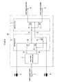
- FIG. 5 is a block diagram showing a functionality structure of an ultrasonic diagnostic apparatus 500 of a third embodiment of the present invention, comprising a semiconductor device according to the first embodiment or the second embodiment of the present invention.
- the ultrasonic diagnostic apparatus 500 comprises; an ultrasonic probe 50 for transmitting and receiving an ultrasonic to and from an internal part of an examinee (not shown) to be measured, a transmission circuit system means 51 for transmission-focus-processing a transmission wave to the ultrasonic probe 50 and transmitting an ultrasonic, a reception circuit system means 52 comprising a phasing means for reception-focus-processing a reception wave output from the ultrasonic probe 50, and switch circuit groups 55 for switching an ultrasonic signal transmitted among the ultrasonic probe 50, and the transmission circuit system means 51, and the reception circuit system means 52.
- the ultrasonic diagnostic apparatus 500 further comprises; an ultrasonic display circuit system means 53 for displaying an ultrasonic tomography image or the like using a reception signal output from the reception circuit system means 52, and an image display 54, for example, a monitor display or the like, for displaying an ultrasonic image information output from the ultrasonic display circuit system means 53.
- signal lines 505, 515, and 552 in bold lines show an ultrasonic transmission/reception signal flow
- signal lines 523, 534, and 565 in fine lines show a control signal flow.
- the ultrasonic probe 50, the transmission circuit system means 51, the reception circuit system means 52, and the ultrasonic display circuit system means 53 are referred to as "probe”, “transmission circuit system”, “reception circuit system”, and “ultrasonic display circuit system”, respectively, for the simplification in the block diagram.
- the ultrasonic diagnostic apparatus 500 of this embodiment comprises a semiconductor device, of the aforementioned embodiment, utilized for the switch circuit groups 55 for switching an ultrasonic signal transmitted among a number m of oscillators equipped in the ultrasonic probe 50 and the transmission circuit system means 51, and the reception circuit system means 52.
- the switch circuit groups 55 are provided among the transmission circuit system means 51, and the reception circuit system means 52, and the ultrasonic probe 50. Incidentally, a number n of the transmission/reception channels are connected between the switch circuit groups 55 and the transmission circuit system means 51, and between the switch circuit groups 55 and the reception circuit system means 52.
- the configuration of the switch circuit groups 55 in FIG. 5 is exemplified in the switch circuit groups 55 in FIG. 6 , in more detail.
- the switch circuit groups 55 consist of a number m of switch circuit groups, that is to say, a switch circuit group #1 through #m, each of which comprises a number n of the switches (semiconductor devices 4 ( FIG. 1 ) and 24 ( FIG. 2 ).
- One terminal of the number n of the switches (semiconductor devices 4 ( FIG. 1 ) and 24 ( FIG. 2 ) comprised in each switch circuit group is connected to each other and to an oscillator comprised in the ultrasonic probe 50. That is to say, each of the commonly-connected terminals in each of the switch circuit group #1 through #m is connected to the one terminal of the oscillator #1 through #m comprised in the ultrasonic probe 50.
- the other terminals of the oscillator #1 through #m are earthed (grounded).
- each of other terminals of a number n of switches (semiconductor devices 4 ( FIG. 1 ) and 24 ( FIG. 2 ) comprised in each of the switch circuit groups is connected to the transmission/reception channel #1 through #n.
- each of the number m of the oscillators comprised in the ultrasonic probe 50 in FIG. 5 corresponds to each of the oscillator #1 through #m in FIG. 6 .
- each of the number n of the transmission/reception channel 515 and 552 in FIG. 5 corresponds to each of the transmission/reception channel #1 through #n in FIG. 6 .
- the switch control circuit 56 selects and controls the switch circuit group (#1 through #m) of the switch circuit groups 55 and a number n of switches (semiconductor devices 4 ( FIG. 1 ) and 24 ( FIG. 2 ) comprised in each thereof, by the control signal 565 ( FIG. 5 ).
- the transmission circuit system means 51 applies a voltage of an approximately one hundred and several dozens of volts to the oscillator #1 through #m and the oscillator transmits an ultrasonic beam to an internal part of an examinee (not shown) to be measured. Meanwhile, after the pre-determined time passes, a reflection wave is detected by the oscillator #1 through #m, furthermore, the transformed electric signal (approximately several dozens of milli-volts) is transmitted to the reception circuit system means 52, thereafter, the signal processing is performed.
- each of the switch circuit group (#1 through #m) in the switch circuit groups 55 selects one out of a plurality of ultrasonic transmission/reception channels for a plurality of oscillators (#1 through #m) to transmit and to receive an ultrasonic in an ultrasonic probe, otherwise shuts down all transmission/reception channels.
- the switches when the oscillator (#1 through #m) transmits an ultrasonic beam, the switches (semiconductor devices 4 ( FIG. 1 ) and 24 ( FIG. 2 ))need to have high blocking voltage characteristics, since an aforementioned high voltage is applied to the switch. Moreover, since a high degree of detection accuracy is required to transmit and to receive an ultrasonic, the switches (semiconductor devices 4 ( FIG. 1 ) and 24 ( FIG. 2 )) need a high linearity and a wide dynamic range.
- An ultrasonic diagnostic apparatus 500 in this embodiment is capable of driving a large amplitude of an ultrasonic signal, by utilizing a semiconductor device in this aforementioned embodiment for a switching apparatus of the ultrasonic signal transmitted among the oscillators, the transmission circuit system, and the reception circuit system. This improves the S/N ratio (signal-to-noise ratio) of the ultrasonic signal and can improve the image quality of the ultrasonic diagnostic apparatus.
- the Zener diode 10 is comprised between the p-type MOSFET 11 and a high-voltage positive power supply 5 (VPP), meanwhile, the Zener diode 10 may be comprised between the p-type MOSFET 11 and the first output line 14.
- the first output line 14 has an effect to maintain a value to add the Zener voltage of the Zener diode 10 to an electrical potential of the voltage of the high-voltage positive power supply (VPP).
- the Zener diode 10 may be formed in the same manufacturing process (common manufacturing process) as the p-type MOSFET 11 and within the same substrate as the p-type MOSFET 11. In the manufacturing process of the p-type MOSFET 11, both of P layer and N layer are manufactured therein. Accordingly, it is possible to manufacture a Zener diode consisting of P layer and N layer within the same substrate as the p-type MOSFET, and furthermore, in the different insulation-isolated domain (SiO 2 layer). Moreover, it is also possible to adjust the Zener voltage characteristics by ion-implanting an impurity into P layer or N layer of the Zener diode.
- the Zener diode 10 may be formed in the same manufacturing process (common manufacturing process), and within the same substrate as the p-type MOSFET 11, n-type MOSFETs 12, 13, 16 and 17, and the level-shift control circuit 3.
- CMOS Complementary Metal Oxide Semiconductor
- the p-type MOSFET and the n-type MOSFET are formed in the same manufacturing process (common manufacturing process), and within the same substrate, it is further possible to manufacture a Zener diode which consists of P layer and N layer. Manufacturing the Zener diode 10 and each of the aforementioned element devices in the same manufacturing process (common manufacturing process) and within the same substrate, results in the further cost reduction.
- FIG. 2 an explanation is made about a case to utilize an IGBT having a built-in Zener diode. Meanwhile, when any specific performance such as an accuracy is required in Zener voltage characteristics of the Zener diode, IGBT and the Zener diode may be configured in separate components.
- a MOSFET to configure the switch circuit 2 is explained by the n-type MOSFET.
- the p-type MOSFET may configure the switch circuit 2.
- the configuration of the driving circuit 1 or 21, and the level-shift control circuit 3 should be modified so as to correspond to a polarity of the p-type
- the p-type MOSFET may be added in parallel to each of n-type MOSFETs 16 and 17 to configure the switch circuit 2.
- the configuration of the driving circuits 1 ( FIG. 1 ) and 21 ( FIG. 2 ), and the level-shift control circuit 3 should be modified so as to include a circuit to drive the added p-type MOSFET.
- FIG. 5 and FIG. 6 an explanation is made about a case to utilize a semiconductor device of the first embodiment or the second embodiment of the present invention for switching the transmission/reception of the ultrasonic signal to the oscillator in the ultrasonic diagnostic apparatus (a switch for separating the wave-transmission pulse generator and the reception amplifier of the ultrasonic signal).
- the semiconductor device may be utilized for switching the transmission, only.
- the semiconductor device of this embodiment may be utilized for switching a probe in the ultrasonic diagnostic apparatus.
- FIG. 7 shows an example to configure a bi-directional analog switch.
- the bi-directional analog switch 114 comprising of the transistors 140 and 138 and a Zener diode 142
- the level-shifter 112 comprising the transistors 116, 118, 120 and 122, the diode 124 and the Zener diode 130.
- This configuration provides a device to widen a dynamic range so as to maintain a linearity as a bi-directional analog switch 114.
- the bi-directional analog switch 114 when the bi-directional analog switch 114 is in a switch-ON state and applies a negative voltage signal to the switch terminal 144, an electric current flows from the power supply 132, through the transistor 118, the diode 124 and the Zener diode 142. Accordingly, all of the electric currents in the level-shifter 112 flow outward from either of the switch terminal 144 or the switch terminal 146. Moreover, when the bi-directional analog switch 114 is in a switch-OFF state, an electric current flows between the power supplies 132 and 134 through the transistors 116 and 122, and the Zener diode 130.
- the bi-directional analog switch 114 is in switch-ON state or in switch-OFF state, an electric current continues flowing as a leak electric current in the level-shifter 112 which is a control circuit. That is to say, the comparison circuit exemplified in FIG. 7 for reference, causes a larger electric power loss.
- the comparison circuit exemplified in FIG. 7 for reference, causes a larger electric power loss.
- a voltage between a gate and a source of the n-type MOSFET in the switch circuit keeps equal to or higher than the Zener voltage within the operation condition of the switch circuit. Therefore, the aforementioned switch circuit achieves a high linearity as a bi-directional analog switch. Furthermore, while the switch circuit keeps a switch-ON state or a switch-OFF state, an insulation is made between the power supplies. Therefore, no leak electric current flows and it is possible to reduce an electric power loss, compared with the prior art.
- all or a part of the driving circuits 1 and 21 including the Zener diode, the switch circuit 2, and a level-shift control circuit 3, are formed in the same manufacturing process (common manufacturing process) and within the same substrate device, into a semiconductor device, and therefore, a cost reduction would be achieved.
- the aforementioned semiconductor device as a bi-directional analog switch, an improvement of a high degree of detection accuracy of the ultrasonic diagnostic apparatus is expected.
- a bi-directional analog switch especially a high-voltage bi-directional analog switch, is utilized firstly in the medical field, and also extensively in an entirety of various industries.
- a high-voltage bi-directional analog switch utilizing a semiconductor device according to this embodiment of the present invention is feasibly to be used not only in a medical field, but also extensively in a field of analog signal switches utilizing a semiconductor for industrial use and for home use, because of a high linearity in the analog characteristics and a low electric power loss suitable for the miniaturization use and the mobility use, and furthermore, because of the low cost.
Description
- The present invention relates to a semiconductor device configuring a high-voltage bi-directioual analog switch and an ultrasonic apparatus using the same.
- High-voltage bi-directional analog switches (hereinafter referred to as "switch", as required) are utilized to allocate signals to a plurality of oscillators equipped in probes, for example, in a field of ultrasonic diagnostic apparatus. When a bi-directional analog switch is utilized for switching signals of the ultrasonic diagnostic apparatus, a high linearity within an operational range is required for the bi-directional analog switch, so as to suppress a signal distortion affecting a picture quality of diagnostic images.
Moreover,JP 2004-531929 A -
US 6 617 906 B1 discloses systems and methods for limiting a voltage to low-voltage devices employing a high-voltage supply. The systems and methods employ voltage limiting devices to bias cascode devices. The cascode devices are serially connected from a high-voltage supply to a low-voltage node. The voltage limiters are serially connected from the high-voltage supply to ground to bias the cascode devices. Current sources are connected In parallel with the voltage limiters except the one connected to ground. If the current sources are set to deliver substantially equal currents, then the order in which the cascode transistors are biased becomes nondeterministic, but the circuit continues to function and the overall supply current is thereby minimized. - However, conventional bi-directional analog switches have not always secured linearities which are sufficiently good. Moreover, in the case of a circuit configuration disclosed in
JP 2004-531929 A - Therefore, the present invention is to solve the aforementioned problem, and an object of the present invention is to provide a semiconductor device of the bi-directional analog switch which has a high linearity and a low electric power loss.
- In addition, another object of the present invention is to provide an ultrasonic diagnostic apparntus, utilizing the aforementioned semiconductor device and having a high degree of detection accuracy.
- In order to solve the aforementioned problem and to achieve the object of the present invention, an apparatus having the features of the appended independent claims is provided. Preferred embodiments of the invention are described in the dependent claims. According to another aspect, an apparatus is a semiconductor device comprising a switch circuit capable of switching ON or switching OFF, bi-directionally and a driving circuit for driving the switch circuit wherein, wherein the driving circuit is connected to a first power supply and a second power supply, a voltage of the first power supply is equal to or higher than a maximum voltage of a signal applied to input/output terminals of the switch circuit, a voltage of the second power supply is equal to or lower than a minimum voltage of a signal applied to input/output terminals of the switch circuit, and moreover, the driving circuit comprises a Zener diode and a p-type MOSFET connected in series between the first power supply and the switch circuit.
- Furthermore, the apparatus is a semiconductor device comprising a switch circuit for enabling switch-ON or switch-OFF in a bi-directional manner and a driving circuit for driving the switch circuit therein, wherein the driving circuit is connected to the first power supply and the second power supply, the voltage of the first power supply is equal to or higher than the maximum voltage of a signal applied to input/output terminals of the switch circuit, the voltage of the second power supply is equal to or lower than the minimum voltage of the signal applied to input/output terminals of the switch circuit, and moreover, the driving circuit comprises a p-type IGBT connected between the first power supply and the switch circuit.
- In addition, the semiconductor device is utilized for a switch of a wave-transmission of an ultrasonic signal to an oseillator, for separation-switching a wave-transmission pulse generator and a reception amplifier of the ultrasonic signal, or for switching a probe.
- According to the above mentioned configuration, the signal voltage for controlling the switch circuit is secured to be higher than a voltage of a signal to input to the input/output terminal of the switch circuit. Therefore, a semiconductor device of a bi-directional analog switch is realized to secure both of a linearity required for the bi-directional analog switch and a low electric power loss.
- Furthermore, according to the above mentioned structure, the ultrasonic diagnostic apparatus has a high degree of detection accuracy, since the apparatus comprises the bi-directional analog switch with characteristics of the high linearity and of a low electric power loss.
- As above mentioned, according to the present invention, a semiconductor device of the bi-directional analog switch, having the high linearity and the low electric power loss, can be provided.
Furthermore, an ultrasonic diagnostic apparatus utilizing the semiconductor device and having a high degree of detection accuracy, can be provided. -
-
FIG. 1 is a circuit diagram showing a configuration of a semiconductor device according to a first embodiment of the present invention; -
FIG. 2 is a circuit diagram showing a configuration of a semiconductor device according to a second embodiment of the present invention; -
FIG. 3 is a sectional view showing a structure of a p-type IGBT comprised by a semiconductor device according to a second embodiment of the present invention; -
FIG. 4 is a schematic diagram showing a relation graph between an input signal amplitude and an impedance between input and output terminals of a switch circuit, of a semiconductor device of the present invention; -
FIG. 5 is a block diagram showing a functionality structure of an ultrasonic diagnostic apparatus utilizing a semiconductor device according to a third embodiment of the present invention; -
FIG. 6 is a circuit diagram showing a partial and detailed configuration of an ultrasonic diagnostic apparatus utilizing a semiconductor device according to a third embodiment of the present invention; and -
FIG. 7 is a circuit diagram showing a configuration of a bi-directional analog switch circuit and a driving circuit thereof of a circuitry technology referred to for comparison. - A first embodiment of the present invention is described below in detail with reference to the accompanying drawings.
FIG. 1 is a circuit diagram showing a configuration according to a first embodiment of the present invention.
InFIG. 1 , a semiconductor device in the first embodiment consists of a bi-directional analog switchoverall circuit 4. - The bi-directional analog switch
overall circuit 4 is configured, comprising adriving circuit 1, aswitch circuit 2, and a level-shift control circuit 3. Moreover, the bi-directional analog switchoverall circuit 4 is connected to a high-voltage positive power supply 5 (VPP, a first power supply), a high-voltage negative power supply 6 (VNN, a second power supply), and a switch control signal input terminal 7, and comprises input/output terminals switch circuit 2. - The
switch circuit 2 is configured, comprising n-type MOSFETs (Metal-Oxide-Semiconductor Field-Effect Transistor) 16 and 17. The n-type MOSFETs FIG. 1 of the n-type MOSFETs
Thus, the drain terminal of the n-type MOSFET 16 is the input/output terminal 8 for theswitch circuit 2 and the drain terminal of the n-type MOSFET 17 is the input/output terminal 9 for theswitch circuit 2. - The gate terminals (gate) connected each other to the n-
type MOSFETs first output line 14 of thedriving circuit 1.
Meanwhile, the source terminals (source) connected each other to the n-type MOSFETs second output line 15 of thedriving circuit 1.
Thefirst output line 14 and thesecond output line 15 of thedriving circuit 1 are controlled by a switch control signal 7, which is disposed at an upstream side of the circuit. That is to say, a change of the switch control signal 7 results in an operation of the level-shift control circuit 3. Thereafter, thedriving circuit 1 operates on the basis of the control signal given by the first level-shift controlcircuit output terminal 18 and the second level-shift controlcircuit output terminal 19 of the level-shift control circuit 3 and switches theswitch circuit 2 into a switch-ON state (on, conduction, low impedance) or a switch-OFF state (off, shut down, high impedance). Thus, a signal applied to the input/output terminal (e.g. input/output terminal 8) is propagated (transmitted) to a counterpart input/output terminal (e.g. input/output terminal 9), or is shut down. - Furthermore, the output signals of the
driving circuit 1 are described as afirst output line 14 and asecond output line 15, instead of a first output signal and a second output signal. This is because each of electrical potentials of thefirst output line 14 and thesecond output line 15, may be occasionally determined by a factor other than an output driven by the p-type MOSFET 11 and the n-type MOSFET 12, and an output driven by the n-type MOSFET 13 in thedriving circuit 1.
Moreover, a detailed configuration and a detailed operation of thedriving circuit 1 and of the level-shift control circuit 3 are described later.
The further detailed operation and the characteristics of theswitch circuit 2 are described later, as well. - The
driving circuit 1 is configured, comprising the Zener diode 10 (including a case that the breakdown voltage is determined by Zener breakdown and by the avalanche yield of this embodiment), the p-type MOSFET 11 and n-type MOSFETs driving circuit 1 is connected to an anode terminal of the Zenerdiode 10 and a cathode terminal of the Zenerdiode 10 is connected to a source terminal of the p-type MOSFET 11.
Meantime, the high-voltage negative power supply 6 (VNN) to be another power supply of thedriving circuit 1 is connected to each of the source terminals of the n-type MOSFETs - A drain terminal of the p-type MOSFET 11 and a drain terminal of the n-
type MOSFET 12 are connected each other, and moreover, output the signal as thefirst output line 14 of thedriving circuit 1.
Furthermore, a drain terminal of the n-type MOSFET 13 outputs a signal as thesecond output line 15 of thedriving circuit 1.
A gate terminal of the p-type MOSFET 11 is connected to the first level-shift controlcircuit output terminal 18 of the level-shift control circuit 3.
A gate terminal of the n-type MOSFET 13 and a gate terminal of the n-type MOSFET 12 are both connected to the second level-shift controlcircuit output terminal 19 of the level-shift control circuit 3. - The level-
shift control circuit 3 is a circuit to voltage-transform the signal and to set the signal so as to drive the drivingcircuit 1 in operation with the high-voltage positive power supply 5 (VPP) and the high-voltage negative power supply 6 (VNN), with the switch control signal 7 (control signal, approximately 0V to 5V). That is to say, the switch control signal, which is between 0V and 5V, is level-shifted (electrical-potential-transformed) into a control signal which is almost equivalent to the voltage VPP or VNN (a voltage difference between VPP and VNN is approximately 200V), at the first level-shift controlcircuit output terminal 18 and at the second level-shift controlcircuit output terminal 19 of the level-shift control circuit 3. Therefore, the gates of the p-type MOSFET 11 and the n-type MOSFET 12 are controlled by approximate values of the electrical potentials of VPP and VNN.
Incidentally, the first level-shift controlcircuit output terminal 18 and the second level-shift controlcircuit output terminal 19 of the level-shift control circuit 3, may be set into a level of the high-voltagenegative power supply 6, simultaneously or with some time difference. - When the first level-shift control
circuit output terminal 18 and the second level-shift controlcircuit output terminal 19 of the level-shift control circuit 3 are set into an electrical potential level of the high-voltage negative power supply 6 (VNN) by the switch control signal 7, the p-type MOSFET 11 of the driving circuit is switched ON and the n-type MOSFETs Zener diode 10 and the p-type MOSFET 11, thereafter, gate capacitances at the n-type MOSFETs switch circuit 2 are charged, and subsequently, gate potentials at the n-type MOSFETs type MOSFETs switch circuit 2 is switched ON. - When the
switch circuit 2 is switched ON and a positive voltage signal is applied to the input/output terminal 8, the voltage of asecond output line 15 connected to the source terminals of the n-type MOSFETs output terminal 8. This is because the n-type MOSFET 13 is switched OFF and the n-type MOSFET 16 is switched ON.
A voltage between the gate sources of the n-type MOSFETs first output line 14 and thesecond output line 15. Afirst output line 14 in the beginning, that is to say, the gate terminal of the n-type MOSFETs circuit 1.
As the electrical potential level (voltage) of the positive voltage signal applied to the input/output terminal 8 rises, the voltage of thesecond output line 15 rises as well, and thereafter, the voltage between the gate sources of the n-type MOSFETs - Here, in order to explain a function of the
Zener diode 10 in this embodiment for easy understanding, a case without theZener diode 10 in thedriving circuit 1 is assumed for comparison.
Assuming that theZener diode 10 does not exist, when a circuit is configured with the p-type MOSFET 11 directly connected to the high-voltage positive power supply 5 (VPP), as a voltage difference between the positive voltage signal applied to the input/output terminal 8 and the voltage of the high-voltage positive power supply 5 (VPP), is getting closer to a threshold voltage of the n-type MOSFETs type MOSFETs
This is because a boundary between the switch-ON and the switch-OFF of the n-type MOSFETs type MOSFETs - Accordingly, when a positive voltage signal applied to the input/
output terminal 8 is transmitted (propagated) to the input/output terminal 9, each of the input/output terminal 8, source electrical potentials (the second output line 15) of the n-type MOSFETs output terminal 9 reaches an electrical potential, which is approximately the same electrical potential as the positive voltage signal applied to the input/output terminal 8.
That is to say, the input/output terminal 8 is not a source (source terminal) of the n-type MOSFETs output terminal 8 is transmitted, an electrical potential of a source (source terminal) of the n-type MOSFETs output terminal 8, as well. - Therefore, as the positive voltage signal applied to the input/
output terminal 8 is getting higher, and as the voltage difference between the electrical potential of the positive voltage signal and the voltage of the high-voltage positive power supply 5 (VPP) is getting closer to the threshold voltage of the n-type MOSFETs type MOSFETs output terminal 9, that is to say, a linearity of theswitch circuit 2 as a bi-directional analog switch is deteriorated. - As shown in
FIG. 1 , a configuration of a circuit connected to theZener diode 10 in this embodiment, is explained.
Since there exists a parasitic capacitance (not shown) between the gate-sources and that between the gate-drains in the n-type MOSFETs output terminal 8 rises, the electrical potential level, which is in proportion to the value of the increase of electrical potential level of the positive voltage signal applied to the input/output terminal 8, increases the gate potential of the n-type MOSFETs - At that moment, in the case of a circuit without the
aforementioned Zener diode 10, the gate potential of the n-type MOSFETs first output line 14, the voltage rise to increase the gate potential of the n-type MOSFETs
However, as shown inFIG. 1 , in the case of a circuit connected with theZener diode 10 in this embodiment, the electrical potential VPP of the high-voltage positive power supply is not applied directly to the gate of the n-type MOSFETs type MOSFETs - This electrical potential rises, at maximum, up to the voltage which is a sum of the voltage of the high-voltage positive power supply 5 (VPP) and the Zener voltage (breakdown voltage) of the
Zener diode 10. Accordingly, even when the electrical potential level of the positive voltage signal applied to the input/output terminal 8 rises, and the voltage difference between the positive voltage signal applied to the input/output terminal 8 and the voltage of the high-voltagepositive power supply 5 is equal to or lower than the threshold voltage of the n-type MOSFETs first output line 14, that is to say, the gate terminal of the n-type MOSFETs Zener diode 10, due to the aforementioned reason. And therefore, in the case of a circuit connected with theZener diode 10, compared with a circuit not connected with theZener diode 10, it is possible to prevent a sharp rise of the impedance and to ensure a wider input signal range in which a linearity of theswitch circuit 2 can be maintained. - Meanwhile, the reason why the aforementioned electrical potential rises, at maximum, up to the voltage which is a sum of the voltage of the high-voltage positive power supply 5 (VPP) and the Zener voltage of the
Zener diode 10, is that a breakdown (avalanche yield) of theZener diode 10 results in a sudden flow of the electric current, when the electrical potential is equal to or higher than the sum of the voltages.
Furthermore, when theZener diode 10 is used in a forward direction, a forward direction voltage drop as a diode, is caused. However, in general, the forward direction voltage drop is set sufficiently lower than each of the Zener voltage (breakdown voltage) and the electrical potential VPP of the high-voltage positive power supply, thus the forward direction voltage drop may be negligible. - Due to the aforementioned reason, for example, when the Zener voltage of the
Zener diode 10 is identical as the threshold voltage of the n-type MOSFETs output terminal 8 may be applied, at maximum, up to the high-voltage positive power supply 5 (VPP) level.
Moreover, since theZener diode 10 has the Zener voltage characteristics, when the gate potential of the n-type MOSFETs Zener diode 10, theZener diode 10 breaks down and flows an electric current, as aforementioned. Accordingly, it is prevented that an unnecessarily high voltage of an element device inside the drivingcircuit 1 or theswitch circuit 2 causes an insulation breakdown of the element device itself or vicinities thereof. - Incidentally, the above mentioned case is that the positive voltage signal is applied to the input/
output terminal 8 and propagated (transmitted) to the input/output terminal 9. The similar effect and characteristics are caused, in case that the positive voltage signal is applied to the input/output terminal 9 and propagated (transmitted) to the input/output terminal 8, since theswitch circuit 2 is of a symmetrical configuration. - Moreover, when a negative voltage signal is applied to the input/
output terminal 8, the value to subtract the source electrical potential and the threshold voltage from the gate electrical potential of the n-type MOSFET 16 is a positive value, which is sufficiently higher than zero. Thus, the n-type MOSFETs output terminal 9, under a condition of a low impedance with little variation, that is to say, under a condition of a high linearity.
Furthermore, when a negative voltage signal is applied to the input/output terminal 9, theswitch circuit 2, because of a symmetrical configuration, propagates (transmits) a negative voltage signal to the input/output terminal 8, under a condition of a low impedance with a small variation, that is to say, under a condition of a high linearity. - As a consequence, a bi-directional analog switch is realized, having a high linearity to an AC signal which is an alternating positive and negative signal and moreover to an AC signal of a large amplitude, by having a high linearity to both of the positive voltage signal and the negative voltage signal.
Incidentally, the measured values of the different impedance characteristics in case with theZener diode 10 and in case without theZener diode 10, is described in detail later. - In order to switch OFF the
switch circuit 2, a first level-shift controlcircuit output terminal 18 and an electrical potential level of a second level-shift controlcircuit output terminal 19 of a level-shift control circuit 3 are set to an electrical potential level of a high-voltagepositive power supply 5. By setting the first level-shift controlcircuit output terminal 18 and the second level-shift controlcircuit output terminal 19 to the electrical potential level of the high-voltage positive power supply 5 (VPP), the p-type MOSFET 11 of the driving circuit is switched OFF, and the n-type MOSFETs type MOSFETs switch circuit 2 is discharged and theswitch circuit 2 is switched OFF. - When this
switch circuit 2 is switched OFF, the p-type MOSFET 11 is switched OFF, and moreover, there is no other path to flow an electric current. Thus, no any electric current flows in a stationary manner between the high-voltage positive power supply 5 (VPP) and the high-voltage negative power supply 6 (VNN). Accordingly, the electric power loss is decreased compared to a comparison circuit which is described later as a reference.
Incidentally, the electrical potential levels, of a first level-shift controlcircuit output terminal 18 and of a second level-shift controlcircuit output terminal 19 of the level-shift control circuit 3, may be set into an electrical potential level of the high-voltage positive power supply 5 (VPP), simultaneously or with some time difference. -
FIG. 2 is a circuit diagram showing a second embodiment of the present invention. InFIG. 2 , a semiconductor device in the second embodiment comprises a bi-directional analog switchoverall circuit 24.
InFIG. 2 of a drivingcircuit 21, comprised in the bi-directional analog switchoverall circuit 24, theZener diode 10 and a p-type MOSFET 11 of adriving circuit 1 inFIG. 1 are substituted with the p-type IGBT (Insulated Gate Bipolar Transistor) 20.
This p-type IGBT, as described later, has a structure to comprise the built-in Zener diode, and therefore, the p-type IGBT may be substituted with theZener diode 10 and the p-type MOSFET 11 inFIG. 1 , accordingly. - In
FIG. 2 , the Zener diode 34 (FIG. 3 ) which is built in to the p-type IGBT 20, has an inverted withstand voltage corresponding to the Zener voltage in a switch-ON state. Accordingly, a configuration comprising the p-type IGBT 20 to switch ON and OFF the high-voltage positive power supply 5 (VPP) and the Zener diode 34 (FIG. 3 ) built in the p-type IGBT 20, has a function and an effect, which are approximately equivalent to a function and an effect of a configuration comprising the p-type MOSFET 11 and aZener diode 10 inFIG. 1 . Therefore, the p-type IGBT 20 ensures a wider input signal range in which aswitch circuit 2 is capable of maintaining a linearity. - Incidentally, the Zener diode 34 (
FIG. 3 ) which is built in to the p-type IGBT 20, as described later, is formed in a side of the collector electrode 33 (FIG. 3 ). That is to say, inFIG. 2 , the Zener diode is formed in a side of afirst output line 14. However, an effect as a Zener diode is the same as the effect inFIG. 1 , even if the Zener diode is not located in a side of the high-voltage positive power supply VPP. Thus, an electrical potential of afirst output line 14 can maintain a value to add the Zener voltage to the voltage of the high-voltage positive power supply (VPP), resulting in a effect to ensure a wider input signal range in which theswitch circuit 2 can maintain a linearity, as aforementioned.
Furthermore, since configurations other than the p-type IGBT 20 are the same as the configurations inFIG. 1 , redundant description thereof will be omitted. -
FIG. 3 is a sectional view showing a structure of a p-type IGBT. InFIG. 3 , anemitter electrode 31 is connected to a P+ layer 351. AnN channel layer 362 lies between the P+ layer 351 and a P-well layer 353. By controlling switch-ON and switch-OFF with agate electrode 32, this part of the structure configures a MOSFET. The structure comprises the aforementioned P-well layer 353, furthermore, aP layer 352, an N+ layer 363 (this part is a bipolar structure), and acollector electrode 33, connected. A major part of the IGBT is configured as above.
In addition, inFIG. 3 , each of an N+ layer 361, an Si substrate (n-) 381, an SiO2 (layer) 371, 372 and 373 is a structurally necessary element to configure IGBT as a device. - In the configuration above, a
diode 34 is configured by the N+ layer 363 and theP layer 352, directly under thecollector electrode 33. Here, by an appropriate selection of an impurity density of theP layer 352 or the N+ layer 363, it is possible to make a diode configured by an N+ layer 363 and theP layer 352, into theZener diode 34. TheZener diode 34 configured by the N+ layer 363 and theP layer 352 gives, in a drivingcircuit 21 ofFIG. 2 , the same effect as theZener diode 10 inFIG. 1 .
Furthermore, a process to manufacture a p-type IGBT as a device, comprises a plurality of processes to configure the P layer, and therefore, by applying an existing ion implantation process or a diffusion process for an appropriate impurity density into theP layer 352 to configure the aforementioned theZener diode 34, it is possible to form theaforementioned Zener diode 34, without adding a new manufacturing process, that is to say, without any cost increase. -
FIG. 4 shows a measurement result of an impedance of the switch circuit 2 (FIG. 1 ) against an input signal amplitude of a circuit inFIG. 1 , and is a characteristics diagram to compare the impedance characteristics in cases with and without theZener diode 10.
InFIG. 4 , a horizontal axis shows a normalized input signal amplitude, and a reference value is set as 1, under a condition that an input signal amplitude is equal to a VPP voltage of the high-voltage positive power supply.
Furthermore, a vertical axis shows a normalized value of an impedance of aswitch circuit 2, and a reference value is set as 1 for an impedance value under a condition that an input signal amplitude is equal to 0.5 (a half of the VPP voltage). - In
FIG. 4 , a region showing almost a flat impedance of a switch circuit 2 (FIG. 1 ) is a range where a linearity is maintained. Acharacteristics line 41 is a measurement result of the circuit not connected with the Zener diode 10 (FIG. 1 ), and meantime, acharacteristics line 42 is a measurement result of the circuit connected with theZener diode 10. By connecting theZener diode 10, a dynamic range of an input signal amplitude becomes wider and a linear domain is extended. In the domain showing a drastic increase of an impedance of thecharacteristics line 41 and thecharacteristics line 42, the difference between thecharacteristics line 41 and thecharacteristics line 42 along the horizontal axis direction, corresponds almost to the Zener voltage of the Zener diode 10 (FIG. 1 ). Incidentally, as aforementioned,FIG. 4 shows a measurement result of the circuit inFIG. 1 , and furthermore, in case that anIGBT 20 ofFIG. 2 is utilized, the built-in Zener diode 34 (FIG. 3 ) causes almost the same characteristics improvement. - Next, an ultrasonic diagnostic apparatus of a third embodiment of the present invention is explained with reference to
FIG. 5 andFIG. 6 .
FIG. 5 is a block diagram showing a functionality structure of an ultrasonic diagnostic apparatus 500 of a third embodiment of the present invention, comprising a semiconductor device according to the first embodiment or the second embodiment of the present invention. - In
FIG. 5 , the ultrasonic diagnostic apparatus 500 comprises; anultrasonic probe 50 for transmitting and receiving an ultrasonic to and from an internal part of an examinee (not shown) to be measured, a transmission circuit system means 51 for transmission-focus-processing a transmission wave to theultrasonic probe 50 and transmitting an ultrasonic, a reception circuit system means 52 comprising a phasing means for reception-focus-processing a reception wave output from theultrasonic probe 50, andswitch circuit groups 55 for switching an ultrasonic signal transmitted among theultrasonic probe 50, and the transmission circuit system means 51, and the reception circuit system means 52. - In addition, the ultrasonic diagnostic apparatus 500 further comprises; an ultrasonic display circuit system means 53 for displaying an ultrasonic tomography image or the like using a reception signal output from the reception circuit system means 52, and an
image display 54, for example, a monitor display or the like, for displaying an ultrasonic image information output from the ultrasonic display circuit system means 53.
Furthermore,signal lines signal lines - Meanwhile, in
FIG. 5 , theultrasonic probe 50, the transmission circuit system means 51, the reception circuit system means 52, and the ultrasonic display circuit system means 53 are referred to as "probe", "transmission circuit system", "reception circuit system", and "ultrasonic display circuit system", respectively, for the simplification in the block diagram. - The ultrasonic diagnostic apparatus 500 of this embodiment comprises a semiconductor device, of the aforementioned embodiment, utilized for the
switch circuit groups 55 for switching an ultrasonic signal transmitted among a number m of oscillators equipped in theultrasonic probe 50 and the transmission circuit system means 51, and the reception circuit system means 52. - The
switch circuit groups 55 are provided among the transmission circuit system means 51, and the reception circuit system means 52, and theultrasonic probe 50. Incidentally, a number n of the transmission/reception channels are connected between theswitch circuit groups 55 and the transmission circuit system means 51, and between theswitch circuit groups 55 and the reception circuit system means 52.
The configuration of theswitch circuit groups 55 inFIG. 5 is exemplified in theswitch circuit groups 55 inFIG. 6 , in more detail. - In
FIG. 6 , theswitch circuit groups 55 consist of a number m of switch circuit groups, that is to say, a switchcircuit group # 1 through #m, each of which comprises a number n of the switches (semiconductor devices 4 (FIG. 1 ) and 24 (FIG. 2 ). One terminal of the number n of the switches (semiconductor devices 4 (FIG. 1 ) and 24 (FIG. 2 ) comprised in each switch circuit group is connected to each other and to an oscillator comprised in theultrasonic probe 50. That is to say, each of the commonly-connected terminals in each of the switchcircuit group # 1 through #m is connected to the one terminal of theoscillator # 1 through #m comprised in theultrasonic probe 50. Furthermore, the other terminals of theoscillator # 1 through #m are earthed (grounded). - Moreover, each of other terminals of a number n of switches (semiconductor devices 4 (
FIG. 1 ) and 24 (FIG. 2 ) comprised in each of the switch circuit groups is connected to the transmission/reception channel # 1 through #n. Incidentally, each of the number m of the oscillators comprised in theultrasonic probe 50 inFIG. 5 corresponds to each of theoscillator # 1 through #m inFIG. 6 .
Meanwhile, each of the number n of the transmission/reception channel FIG. 5 corresponds to each of the transmission/reception channel # 1 through #n inFIG. 6 . - Furthermore, the switch control circuit 56 (
FIG. 5 ) selects and controls the switch circuit group (#1 through #m) of theswitch circuit groups 55 and a number n of switches (semiconductor devices 4 (FIG. 1 ) and 24 (FIG. 2 ) comprised in each thereof, by the control signal 565 (FIG. 5 ). - In the aforementioned configuration, the transmission circuit system means 51 applies a voltage of an approximately one hundred and several dozens of volts to the
oscillator # 1 through #m and the oscillator transmits an ultrasonic beam to an internal part of an examinee (not shown) to be measured. Meanwhile, after the pre-determined time passes, a reflection wave is detected by theoscillator # 1 through #m, furthermore, the transformed electric signal (approximately several dozens of milli-volts) is transmitted to the reception circuit system means 52, thereafter, the signal processing is performed.
In the processes above, each of the switch circuit group (#1 through #m) in theswitch circuit groups 55 selects one out of a plurality of ultrasonic transmission/reception channels for a plurality of oscillators (#1 through #m) to transmit and to receive an ultrasonic in an ultrasonic probe, otherwise shuts down all transmission/reception channels. - Furthermore, when the oscillator (#1 through #m) transmits an ultrasonic beam, the switches (semiconductor devices 4 (
FIG. 1 ) and 24 (FIG. 2 ))need to have high blocking voltage characteristics, since an aforementioned high voltage is applied to the switch. Moreover, since a high degree of detection accuracy is required to transmit and to receive an ultrasonic, the switches (semiconductor devices 4 (FIG. 1 ) and 24 (FIG. 2 )) need a high linearity and a wide dynamic range. - An ultrasonic diagnostic apparatus 500 in this embodiment is capable of driving a large amplitude of an ultrasonic signal, by utilizing a semiconductor device in this aforementioned embodiment for a switching apparatus of the ultrasonic signal transmitted among the oscillators, the transmission circuit system, and the reception circuit system. This improves the S/N ratio (signal-to-noise ratio) of the ultrasonic signal and can improve the image quality of the ultrasonic diagnostic apparatus.
- In
FIG. 1 , theZener diode 10 is comprised between the p-type MOSFET 11 and a high-voltage positive power supply 5 (VPP), meanwhile, theZener diode 10 may be comprised between the p-type MOSFET 11 and thefirst output line 14. In either case that theZener diode 10 is comprised in a side of the source or in a side of the drain of the p-type MOSFET 11, thefirst output line 14 has an effect to maintain a value to add the Zener voltage of theZener diode 10 to an electrical potential of the voltage of the high-voltage positive power supply (VPP). - Furthermore, the
Zener diode 10 may be formed in the same manufacturing process (common manufacturing process) as the p-type MOSFET 11 and within the same substrate as the p-type MOSFET 11. In the manufacturing process of the p-type MOSFET 11, both of P layer and N layer are manufactured therein. Accordingly, it is possible to manufacture a Zener diode consisting of P layer and N layer within the same substrate as the p-type MOSFET, and furthermore, in the different insulation-isolated domain (SiO2 layer). Moreover, it is also possible to adjust the Zener voltage characteristics by ion-implanting an impurity into P layer or N layer of the Zener diode. - In addition, the
Zener diode 10 may be formed in the same manufacturing process (common manufacturing process), and within the same substrate as the p-type MOSFET 11, n-type MOSFETs shift control circuit 3.
In the manufacturing process of CMOS (Complementary Metal Oxide Semiconductor), since the p-type MOSFET and the n-type MOSFET are formed in the same manufacturing process (common manufacturing process), and within the same substrate, it is further possible to manufacture a Zener diode which consists of P layer and N layer. Manufacturing theZener diode 10 and each of the aforementioned element devices in the same manufacturing process (common manufacturing process) and within the same substrate, results in the further cost reduction. - Furthermore, in
FIG. 2 , an explanation is made about a case to utilize an IGBT having a built-in Zener diode. Meanwhile, when any specific performance such as an accuracy is required in Zener voltage characteristics of the Zener diode, IGBT and the Zener diode may be configured in separate components. - Moreover, in
FIG. 1 andFIG. 2 , a MOSFET to configure theswitch circuit 2, is explained by the n-type MOSFET. Meanwhile, the p-type MOSFET may configure theswitch circuit 2. In this case, however, the configuration of the drivingcircuit shift control circuit 3 should be modified so as to correspond to a polarity of the p-type - In addition, in
FIG. 1 andFIG. 2 , the p-type MOSFET may be added in parallel to each of n-type MOSFETs switch circuit 2. In this case, however, the configuration of the driving circuits 1 (FIG. 1 ) and 21 (FIG. 2 ), and the level-shift control circuit 3 should be modified so as to include a circuit to drive the added p-type MOSFET. - Furthermore, in
FIG. 5 andFIG. 6 , an explanation is made about a case to utilize a semiconductor device of the first embodiment or the second embodiment of the present invention for switching the transmission/reception of the ultrasonic signal to the oscillator in the ultrasonic diagnostic apparatus (a switch for separating the wave-transmission pulse generator and the reception amplifier of the ultrasonic signal). However, the semiconductor device may be utilized for switching the transmission, only.
Moreover, the semiconductor device of this embodiment may be utilized for switching a probe in the ultrasonic diagnostic apparatus. - As a comparable circuit technology for reference, a configuration of the bi-directional analog switch circuit and the driving circuit thereof, is shown in
FIG. 7 .
FIG. 7 shows an example to configure a bi-directional analog switch. InFIG. 7 , thebi-directional analog switch 114 comprising of thetransistors Zener diode 142, is controlled by the level-shifter 112 comprising thetransistors diode 124 and theZener diode 130.
This configuration provides a device to widen a dynamic range so as to maintain a linearity as abi-directional analog switch 114. - However, when the
bi-directional analog switch 114 is in a switch-ON state and applies a negative voltage signal to theswitch terminal 144, an electric current flows from thepower supply 132, through thetransistor 118, thediode 124 and theZener diode 142. Accordingly, all of the electric currents in the level-shifter 112 flow outward from either of theswitch terminal 144 or theswitch terminal 146.
Moreover, when thebi-directional analog switch 114 is in a switch-OFF state, an electric current flows between the power supplies 132 and 134 through thetransistors Zener diode 130. - Accordingly, in either case that the
bi-directional analog switch 114 is in switch-ON state or in switch-OFF state, an electric current continues flowing as a leak electric current in the level-shifter 112 which is a control circuit. That is to say, the comparison circuit exemplified inFIG. 7 for reference, causes a larger electric power loss.
To the contrary, in the case of a semiconductor device which is a bi-directional analog switch of this aforementioned embodiment, there is no path to flow a leak electric current which flows in the comparison circuit mentioned above, and therefore, an electric power loss is reduced. - As aforementioned in this embodiment, by utilizing the p-type MOSFET and the Zener diode connected in series, or by connecting the p-type IGBT with the built-in Zener diode, a voltage between a gate and a source of the n-type MOSFET in the switch circuit keeps equal to or higher than the Zener voltage within the operation condition of the switch circuit. Therefore, the aforementioned switch circuit achieves a high linearity as a bi-directional analog switch.
Furthermore, while the switch circuit keeps a switch-ON state or a switch-OFF state, an insulation is made between the power supplies. Therefore, no leak electric current flows and it is possible to reduce an electric power loss, compared with the prior art.
In addition, all or a part of the drivingcircuits switch circuit 2, and a level-shift control circuit 3, are formed in the same manufacturing process (common manufacturing process) and within the same substrate device, into a semiconductor device, and therefore, a cost reduction would be achieved.
Moreover, by comprising the aforementioned semiconductor device as a bi-directional analog switch, an improvement of a high degree of detection accuracy of the ultrasonic diagnostic apparatus is expected. - A bi-directional analog switch, especially a high-voltage bi-directional analog switch, is utilized firstly in the medical field, and also extensively in an entirety of various industries. A high-voltage bi-directional analog switch utilizing a semiconductor device according to this embodiment of the present invention, is feasibly to be used not only in a medical field, but also extensively in a field of analog signal switches utilizing a semiconductor for industrial use and for home use, because of a high linearity in the analog characteristics and a low electric power loss suitable for the miniaturization use and the mobility use, and furthermore, because of the low cost.
Claims (7)
- A semiconductor device comprising:a switch circuit (2) capable of switching ON or switching OFF, bi-direciionally; anda driving circuit (1) for driving the switch circuit (2), whereinthe driving circuit (1) is connected to a first power supply (VPP) comprising a first power supply voltage which is equal to or higher than a maximum voltage of the voltage signal applied to the input/output terminals (8, 9) of the switch circuit (2), and the driving circuit (1) is connected to a second power supply (VNN) comprising a second power supply voltage which is equal to or
lower than a minimum voltage of the voltage signal applied to the input/output terminals (8,9) of the switch circuit (2); andthe driving circuit (1) comprises a Zener diode (10) and a p-type MOSFET (11) connected in series between the first power supply (VPP) and the switch circuit (2),
characterized in that the switch circuit has first and second n-type MOSFETs (16, 17) whose sources are connected with each other, whose gates are connected with each other, and whose drains are used as input/output terminals (8, 9) to which a voltage signal which is positive or negative is applied; output voltages from the driving circuit (1) are applied to the gates and the sources respecfively. - A semiconductor device as claimed in Claim 1, further comprising a level-shift control circuit (3) for level-shifting a switch control signal to control the driving circuit (1).
- A semiconductor device as claimed in Claim 2, wherein the driving circuit (1) comprises the Zener diode (10) and the p-type MOSFET (11), the switch circuit (2), and the level-shift control circuit (3) are formed in a common manufacturing process and within a same substrate.
- A semiconductor device as claimed in Claim 1, wherein a Zener voltage of the Zener diode (10) is equal to or higher than a threshold voltage of the n-type MOSFETs (16, 17) of the switch circuit (2).
- A semiconductor device comprising:- a switch circuit (2) capable of switching ON or switching OFF, bi-directionally; and
a driving circuit (1) for driving the switch circuit (2), wherein the driving circuit (1) is connected to a first power supply (VPP) comprising a first power supply voltage which is equal to or higher than a maximum voltage of the voltage signal applied to the input/output terminals (8, 9) of the switch circuit (2), and the driving circuit (1) is connected to a second power supply (VNN) comprising a second power supply voltage which is equal to or lower than a minimum voltage of the voltage signal applied to the input/output terminal (8, 9) of the switch circuit (2); and the driving circuit (1) comprises a p-type IGBT (20) connected between the first power supply (VPP) and the switch circuit (20); and a Zener diode (34) is configured by semiconductor layers (352, 363) which constitute the p-type IGBT (20) in a side of a collector electrode (33), characterized in that
the switch circuit (2) has first and second n-type MOSFETs (16, 17) whose sources are connected with each other, whose gates are connected with each other, and whose drains are used as input/output terminals (8, 9) to which a voltage signal which is positive or negative is applied;
output voltages from the driving circuit (1) are applied to the gates and
the sources respectively. - A semiconductor device as claimed in Claim 5, wherein a Zener voltage of the Zener diode (34) is equal to or higher than a threshold voltage of the n-type MOSFETs (16, 17) of the switch circuit (2).
- An ultrasonic diagnostic apparatus, wherein the semiconductor device as claimed In any one of Claims 1 to 6 is utilized for switching a wave-transmission of an ultrasonic signal to an oscillator,
separation-switching a wave-transmission pulse generator and a reception amplifier of the ultrasonic signal; or
switching a probe.
Applications Claiming Priority (1)
| Application Number | Priority Date | Filing Date | Title |
|---|---|---|---|
| JP2010241711A JP5485108B2 (en) | 2010-10-28 | 2010-10-28 | Semiconductor device and ultrasonic diagnostic apparatus using the same |
Publications (2)
| Publication Number | Publication Date |
|---|---|
| EP2448120A1 EP2448120A1 (en) | 2012-05-02 |
| EP2448120B1 true EP2448120B1 (en) | 2013-07-17 |
Family
ID=45023595
Family Applications (1)
| Application Number | Title | Priority Date | Filing Date |
|---|---|---|---|
| EP11187070.5A Active EP2448120B1 (en) | 2010-10-28 | 2011-10-28 | Semiconductor device and ultrasonic diagnostic apparatus using the same |
Country Status (4)
| Country | Link |
|---|---|
| US (1) | US9190992B2 (en) |
| EP (1) | EP2448120B1 (en) |
| JP (1) | JP5485108B2 (en) |
| CN (1) | CN102545860B (en) |
Families Citing this family (20)
| Publication number | Priority date | Publication date | Assignee | Title |
|---|---|---|---|---|
| US9157897B2 (en) * | 2009-10-21 | 2015-10-13 | Texas Instruments Incorporated | High voltage ultrasound transmitter with gate protection diodes and intrinsic output zeroing |
| US9669427B2 (en) * | 2012-01-24 | 2017-06-06 | Texas Instruments Incorporated | Methods and systems for ultrasound control with bi-directional transistor |
| JP6071405B2 (en) * | 2012-10-15 | 2017-02-01 | 日置電機株式会社 | Switch device |
| JP6154705B2 (en) * | 2013-09-24 | 2017-06-28 | 株式会社 日立パワーデバイス | Semiconductor switch circuit, signal processing apparatus, and ultrasonic diagnostic apparatus |
| JP6202975B2 (en) * | 2013-10-08 | 2017-09-27 | 株式会社アドバンテスト | Switch device and test device |
| JP6375648B2 (en) * | 2014-03-13 | 2018-08-22 | コニカミノルタ株式会社 | Acoustic sensor and ultrasonic probe |
| US9406754B2 (en) * | 2014-07-30 | 2016-08-02 | Infineon Technologies Ag | Smart semiconductor switch |
| JP6563180B2 (en) | 2014-08-07 | 2019-08-21 | エイブリック株式会社 | Semiconductor integrated circuit device |
| EP3224952B1 (en) * | 2014-11-24 | 2021-10-06 | Bang & Olufsen A/S | Solid state switch relay |
| DE102015109167B3 (en) * | 2015-06-10 | 2016-08-11 | Weetech Gmbh | Bidirectional MOSFET switch and multiplexer |
| US10082565B2 (en) | 2016-03-31 | 2018-09-25 | Butterfly Network, Inc. | Multilevel bipolar pulser |
| US9778348B1 (en) * | 2016-03-31 | 2017-10-03 | Butterfly Network, Inc. | Symmetric receiver switch for bipolar pulser |
| US11607199B2 (en) * | 2018-11-20 | 2023-03-21 | Siemens Medical Solutions Usa, Inc. | Switched capacitor for elasticity mode imaging with ultrasound |
| GB2579678B (en) | 2018-12-11 | 2021-10-06 | Cirrus Logic Int Semiconductor Ltd | Switch arrangements |
| US10855258B1 (en) | 2019-08-16 | 2020-12-01 | Cirrus Logic, Inc. | Voltage control |
| EP4031903A4 (en) | 2019-09-19 | 2023-09-20 | BFLY Operations, Inc. | Symmetric receiver switch for ultrasound devices |
| CN111342824A (en) * | 2020-05-19 | 2020-06-26 | 佛山市联动科技股份有限公司 | High-current fast electronic switch |
| CN111884628A (en) * | 2020-07-30 | 2020-11-03 | 武汉博畅通信设备有限责任公司 | Negative high-voltage driving circuit of PIN diode |
| CN112929015B (en) * | 2021-01-22 | 2023-10-31 | 东芯半导体股份有限公司 | switching circuit |
| CN114076938B (en) * | 2022-01-19 | 2022-06-03 | 深圳市勃望初芯半导体科技有限公司 | High-integration ultrasonic transmitting and receiving-transmitting switching chip |
Family Cites Families (10)
| Publication number | Priority date | Publication date | Assignee | Title |
|---|---|---|---|---|
| US6509781B2 (en) * | 2001-03-20 | 2003-01-21 | Koninklijke Philips Electronics N.V. | Circuit and method for controlling a dynamic, bi-directional high voltage analog switch |
| US6617906B1 (en) * | 2002-10-01 | 2003-09-09 | Texas Instruments Incorporated | Low-current compliance stack using nondeterministically biased Zener strings |
| JP2006033723A (en) | 2004-07-21 | 2006-02-02 | Sharp Corp | Optical coupling element for power control and electronic equipment using it |
| JP4455972B2 (en) | 2004-10-08 | 2010-04-21 | 三菱電機株式会社 | Semiconductor device |
| JP4096948B2 (en) * | 2005-02-01 | 2008-06-04 | セイコーエプソン株式会社 | Level shift circuit, electro-optical device using the same, and electronic apparatus |
| JP4618164B2 (en) | 2005-09-20 | 2011-01-26 | 株式会社デンソー | Switch circuit |
| JP2008042950A (en) * | 2006-08-01 | 2008-02-21 | Mitsubishi Electric Corp | Power transformer |
| US7982239B2 (en) | 2007-06-13 | 2011-07-19 | Northrop Grumman Corporation | Power switching transistors |
| JP2009111304A (en) | 2007-11-01 | 2009-05-21 | Fuji Electric Device Technology Co Ltd | Overvoltage protective function built-in mos semiconductor apparatus and method of manufacturing the same |
| US20110028845A1 (en) * | 2009-07-31 | 2011-02-03 | Bruno Hans Haider | Reconfigurable Ultrasound Array with Low Noise CW Processing |
-
2010
- 2010-10-28 JP JP2010241711A patent/JP5485108B2/en active Active
-
2011
- 2011-10-27 US US13/282,882 patent/US9190992B2/en active Active
- 2011-10-28 EP EP11187070.5A patent/EP2448120B1/en active Active
- 2011-10-28 CN CN201110339574.8A patent/CN102545860B/en active Active
Also Published As
| Publication number | Publication date |
|---|---|
| CN102545860A (en) | 2012-07-04 |
| EP2448120A1 (en) | 2012-05-02 |
| US9190992B2 (en) | 2015-11-17 |
| JP5485108B2 (en) | 2014-05-07 |
| JP2012095168A (en) | 2012-05-17 |
| US20120108963A1 (en) | 2012-05-03 |
| CN102545860B (en) | 2015-02-25 |
Similar Documents
| Publication | Publication Date | Title |
|---|---|---|
| EP2448120B1 (en) | Semiconductor device and ultrasonic diagnostic apparatus using the same | |
| US9455711B2 (en) | Semiconductor integrated circuit device | |
| US9531368B2 (en) | Semiconductor switch circuit, signal processing apparatus, and ultrasound diagnostic apparatus | |
| KR102435299B1 (en) | Multilevel bipolar pulsar | |
| US9178507B2 (en) | Apparatus and methods for ultrasound transmit switching | |
| US10211826B2 (en) | Electronic switch, and corresponding device and method | |
| US9479162B2 (en) | Apparatus and methods for ultrasound probes | |
| US10312906B2 (en) | Switch apparatus | |
| US9568597B2 (en) | Ultrasound capacitive T/R switch device, circuit | |
| JP4635713B2 (en) | Switch circuit, semiconductor device, ultrasonic diagnostic device, semiconductor tester | |
| US9337823B2 (en) | Switching circuit and semiconductor integrated circuit device | |
| US20220206523A1 (en) | Voltage converter | |
| US9893175B2 (en) | Integrated circuit with a power transistor and a driver circuit integrated in a common semiconductor body | |
| JP2013197929A (en) | Semiconductor device, and ultrasonic diagnostic apparatus using the same | |
| JPWO2008035532A1 (en) | Switch device and test device | |
| US6313513B1 (en) | AC switch device used for switching AC circuit and AC switch circuit having the AC switch device | |
| US10312913B2 (en) | Level shifter | |
| US20130257514A1 (en) | Source-follower based voltage mode transmitter | |
| CN105897246B (en) | Voltage level shifter for high voltage applications | |
| US8836027B2 (en) | Switch circuit using LDMOS element | |
| JP2023042299A (en) | Semiconductor device | |
| JP2005286664A (en) | Clamp circuit | |
| JPH04301919A (en) | Switching circuit |
Legal Events
| Date | Code | Title | Description |
|---|---|---|---|
| PUAI | Public reference made under article 153(3) epc to a published international application that has entered the european phase |
Free format text: ORIGINAL CODE: 0009012 |
|
| 17P | Request for examination filed |
Effective date: 20120309 |
|
| AK | Designated contracting states |
Kind code of ref document: A1 Designated state(s): AL AT BE BG CH CY CZ DE DK EE ES FI FR GB GR HR HU IE IS IT LI LT LU LV MC MK MT NL NO PL PT RO RS SE SI SK SM TR |
|
| AX | Request for extension of the european patent |
Extension state: BA ME |
|
| GRAP | Despatch of communication of intention to grant a patent |
Free format text: ORIGINAL CODE: EPIDOSNIGR1 |
|
| GRAS | Grant fee paid |
Free format text: ORIGINAL CODE: EPIDOSNIGR3 |
|
| GRAA | (expected) grant |
Free format text: ORIGINAL CODE: 0009210 |
|
| AK | Designated contracting states |
Kind code of ref document: B1 Designated state(s): AL AT BE BG CH CY CZ DE DK EE ES FI FR GB GR HR HU IE IS IT LI LT LU LV MC MK MT NL NO PL PT RO RS SE SI SK SM TR |
|
| REG | Reference to a national code |
Ref country code: GB Ref legal event code: FG4D |
|
| REG | Reference to a national code |
Ref country code: CH Ref legal event code: EP |
|
| REG | Reference to a national code |
Ref country code: IE Ref legal event code: FG4D |
|
| REG | Reference to a national code |
Ref country code: AT Ref legal event code: REF Ref document number: 622739 Country of ref document: AT Kind code of ref document: T Effective date: 20130815 |
|
| REG | Reference to a national code |
Ref country code: DE Ref legal event code: R096 Ref document number: 602011002391 Country of ref document: DE Effective date: 20130912 |
|
| REG | Reference to a national code |
Ref country code: NL Ref legal event code: T3 |
|
| REG | Reference to a national code |
Ref country code: AT Ref legal event code: MK05 Ref document number: 622739 Country of ref document: AT Kind code of ref document: T Effective date: 20130717 |
|
| REG | Reference to a national code |
Ref country code: LT Ref legal event code: MG4D |
|
| PG25 | Lapsed in a contracting state [announced via postgrant information from national office to epo] |
Ref country code: HR Free format text: LAPSE BECAUSE OF FAILURE TO SUBMIT A TRANSLATION OF THE DESCRIPTION OR TO PAY THE FEE WITHIN THE PRESCRIBED TIME-LIMIT Effective date: 20130717 Ref country code: BE Free format text: LAPSE BECAUSE OF FAILURE TO SUBMIT A TRANSLATION OF THE DESCRIPTION OR TO PAY THE FEE WITHIN THE PRESCRIBED TIME-LIMIT Effective date: 20130717 Ref country code: SE Free format text: LAPSE BECAUSE OF FAILURE TO SUBMIT A TRANSLATION OF THE DESCRIPTION OR TO PAY THE FEE WITHIN THE PRESCRIBED TIME-LIMIT Effective date: 20130717 Ref country code: CY Free format text: LAPSE BECAUSE OF FAILURE TO SUBMIT A TRANSLATION OF THE DESCRIPTION OR TO PAY THE FEE WITHIN THE PRESCRIBED TIME-LIMIT Effective date: 20130821 Ref country code: IS Free format text: LAPSE BECAUSE OF FAILURE TO SUBMIT A TRANSLATION OF THE DESCRIPTION OR TO PAY THE FEE WITHIN THE PRESCRIBED TIME-LIMIT Effective date: 20131117 Ref country code: AT Free format text: LAPSE BECAUSE OF FAILURE TO SUBMIT A TRANSLATION OF THE DESCRIPTION OR TO PAY THE FEE WITHIN THE PRESCRIBED TIME-LIMIT Effective date: 20130717 Ref country code: PT Free format text: LAPSE BECAUSE OF FAILURE TO SUBMIT A TRANSLATION OF THE DESCRIPTION OR TO PAY THE FEE WITHIN THE PRESCRIBED TIME-LIMIT Effective date: 20131118 Ref country code: LT Free format text: LAPSE BECAUSE OF FAILURE TO SUBMIT A TRANSLATION OF THE DESCRIPTION OR TO PAY THE FEE WITHIN THE PRESCRIBED TIME-LIMIT Effective date: 20130717 Ref country code: NO Free format text: LAPSE BECAUSE OF FAILURE TO SUBMIT A TRANSLATION OF THE DESCRIPTION OR TO PAY THE FEE WITHIN THE PRESCRIBED TIME-LIMIT Effective date: 20131017 |
|
| PG25 | Lapsed in a contracting state [announced via postgrant information from national office to epo] |
Ref country code: PL Free format text: LAPSE BECAUSE OF FAILURE TO SUBMIT A TRANSLATION OF THE DESCRIPTION OR TO PAY THE FEE WITHIN THE PRESCRIBED TIME-LIMIT Effective date: 20130717 Ref country code: FI Free format text: LAPSE BECAUSE OF FAILURE TO SUBMIT A TRANSLATION OF THE DESCRIPTION OR TO PAY THE FEE WITHIN THE PRESCRIBED TIME-LIMIT Effective date: 20130717 Ref country code: GR Free format text: LAPSE BECAUSE OF FAILURE TO SUBMIT A TRANSLATION OF THE DESCRIPTION OR TO PAY THE FEE WITHIN THE PRESCRIBED TIME-LIMIT Effective date: 20131018 Ref country code: LV Free format text: LAPSE BECAUSE OF FAILURE TO SUBMIT A TRANSLATION OF THE DESCRIPTION OR TO PAY THE FEE WITHIN THE PRESCRIBED TIME-LIMIT Effective date: 20130717 Ref country code: ES Free format text: LAPSE BECAUSE OF FAILURE TO SUBMIT A TRANSLATION OF THE DESCRIPTION OR TO PAY THE FEE WITHIN THE PRESCRIBED TIME-LIMIT Effective date: 20131028 Ref country code: SI Free format text: LAPSE BECAUSE OF FAILURE TO SUBMIT A TRANSLATION OF THE DESCRIPTION OR TO PAY THE FEE WITHIN THE PRESCRIBED TIME-LIMIT Effective date: 20130717 |
|
| PG25 | Lapsed in a contracting state [announced via postgrant information from national office to epo] |
Ref country code: CY Free format text: LAPSE BECAUSE OF FAILURE TO SUBMIT A TRANSLATION OF THE DESCRIPTION OR TO PAY THE FEE WITHIN THE PRESCRIBED TIME-LIMIT Effective date: 20130717 |
|
| PG25 | Lapsed in a contracting state [announced via postgrant information from national office to epo] |
Ref country code: CZ Free format text: LAPSE BECAUSE OF FAILURE TO SUBMIT A TRANSLATION OF THE DESCRIPTION OR TO PAY THE FEE WITHIN THE PRESCRIBED TIME-LIMIT Effective date: 20130717 Ref country code: RO Free format text: LAPSE BECAUSE OF FAILURE TO SUBMIT A TRANSLATION OF THE DESCRIPTION OR TO PAY THE FEE WITHIN THE PRESCRIBED TIME-LIMIT Effective date: 20130717 Ref country code: DK Free format text: LAPSE BECAUSE OF FAILURE TO SUBMIT A TRANSLATION OF THE DESCRIPTION OR TO PAY THE FEE WITHIN THE PRESCRIBED TIME-LIMIT Effective date: 20130717 Ref country code: EE Free format text: LAPSE BECAUSE OF FAILURE TO SUBMIT A TRANSLATION OF THE DESCRIPTION OR TO PAY THE FEE WITHIN THE PRESCRIBED TIME-LIMIT Effective date: 20130717 Ref country code: SK Free format text: LAPSE BECAUSE OF FAILURE TO SUBMIT A TRANSLATION OF THE DESCRIPTION OR TO PAY THE FEE WITHIN THE PRESCRIBED TIME-LIMIT Effective date: 20130717 |
|
| PLBE | No opposition filed within time limit |
Free format text: ORIGINAL CODE: 0009261 |
|
| STAA | Information on the status of an ep patent application or granted ep patent |
Free format text: STATUS: NO OPPOSITION FILED WITHIN TIME LIMIT |
|
| PG25 | Lapsed in a contracting state [announced via postgrant information from national office to epo] |
Ref country code: MC Free format text: LAPSE BECAUSE OF FAILURE TO SUBMIT A TRANSLATION OF THE DESCRIPTION OR TO PAY THE FEE WITHIN THE PRESCRIBED TIME-LIMIT Effective date: 20130717 |
|
| 26N | No opposition filed |
Effective date: 20140422 |
|
| REG | Reference to a national code |
Ref country code: IE Ref legal event code: MM4A |
|
| REG | Reference to a national code |
Ref country code: DE Ref legal event code: R097 Ref document number: 602011002391 Country of ref document: DE Effective date: 20140422 |
|
| PG25 | Lapsed in a contracting state [announced via postgrant information from national office to epo] |
Ref country code: IE Free format text: LAPSE BECAUSE OF NON-PAYMENT OF DUE FEES Effective date: 20131028 |
|
| REG | Reference to a national code |
Ref country code: GB Ref legal event code: 732E Free format text: REGISTERED BETWEEN 20141204 AND 20141211 |
|
| REG | Reference to a national code |
Ref country code: FR Ref legal event code: TP Owner name: HITACHI POWER SEMICONDUCTOR DEVICE, LTD., JP Effective date: 20141209 |
|
| REG | Reference to a national code |
Ref country code: NL Ref legal event code: SD Effective date: 20150304 |
|
| PG25 | Lapsed in a contracting state [announced via postgrant information from national office to epo] |
Ref country code: SM Free format text: LAPSE BECAUSE OF FAILURE TO SUBMIT A TRANSLATION OF THE DESCRIPTION OR TO PAY THE FEE WITHIN THE PRESCRIBED TIME-LIMIT Effective date: 20130717 |
|
| REG | Reference to a national code |
Ref country code: CH Ref legal event code: PL |
|
| PG25 | Lapsed in a contracting state [announced via postgrant information from national office to epo] |
Ref country code: TR Free format text: LAPSE BECAUSE OF FAILURE TO SUBMIT A TRANSLATION OF THE DESCRIPTION OR TO PAY THE FEE WITHIN THE PRESCRIBED TIME-LIMIT Effective date: 20130717 |
|
| PG25 | Lapsed in a contracting state [announced via postgrant information from national office to epo] |
Ref country code: MK Free format text: LAPSE BECAUSE OF FAILURE TO SUBMIT A TRANSLATION OF THE DESCRIPTION OR TO PAY THE FEE WITHIN THE PRESCRIBED TIME-LIMIT Effective date: 20130717 Ref country code: LI Free format text: LAPSE BECAUSE OF NON-PAYMENT OF DUE FEES Effective date: 20141031 Ref country code: CH Free format text: LAPSE BECAUSE OF NON-PAYMENT OF DUE FEES Effective date: 20141031 Ref country code: RS Free format text: LAPSE BECAUSE OF FAILURE TO SUBMIT A TRANSLATION OF THE DESCRIPTION OR TO PAY THE FEE WITHIN THE PRESCRIBED TIME-LIMIT Effective date: 20131017 Ref country code: BG Free format text: LAPSE BECAUSE OF FAILURE TO SUBMIT A TRANSLATION OF THE DESCRIPTION OR TO PAY THE FEE WITHIN THE PRESCRIBED TIME-LIMIT Effective date: 20130717 Ref country code: HU Free format text: LAPSE BECAUSE OF FAILURE TO SUBMIT A TRANSLATION OF THE DESCRIPTION OR TO PAY THE FEE WITHIN THE PRESCRIBED TIME-LIMIT; INVALID AB INITIO Effective date: 20111028 Ref country code: LU Free format text: LAPSE BECAUSE OF NON-PAYMENT OF DUE FEES Effective date: 20131028 |
|
| PG25 | Lapsed in a contracting state [announced via postgrant information from national office to epo] |
Ref country code: MT Free format text: LAPSE BECAUSE OF FAILURE TO SUBMIT A TRANSLATION OF THE DESCRIPTION OR TO PAY THE FEE WITHIN THE PRESCRIBED TIME-LIMIT Effective date: 20130717 |
|
| REG | Reference to a national code |
Ref country code: DE Ref legal event code: R082 Ref document number: 602011002391 Country of ref document: DE Representative=s name: MERH-IP MATIAS ERNY REICHL HOFFMANN, DE Ref country code: DE Ref legal event code: R081 Ref document number: 602011002391 Country of ref document: DE Owner name: HITACHI POWER SEMICONDUCTOR DEVICE, LTD., HITA, JP Free format text: FORMER OWNER: HITACHI, LTD., TOKYO, JP Ref country code: DE Ref legal event code: R082 Ref document number: 602011002391 Country of ref document: DE Representative=s name: MERH-IP MATIAS ERNY REICHL HOFFMANN PATENTANWA, DE |
|
| REG | Reference to a national code |
Ref country code: FR Ref legal event code: PLFP Year of fee payment: 6 |
|
| REG | Reference to a national code |
Ref country code: FR Ref legal event code: PLFP Year of fee payment: 7 |
|
| REG | Reference to a national code |
Ref country code: FR Ref legal event code: PLFP Year of fee payment: 8 |
|
| PG25 | Lapsed in a contracting state [announced via postgrant information from national office to epo] |
Ref country code: AL Free format text: LAPSE BECAUSE OF FAILURE TO SUBMIT A TRANSLATION OF THE DESCRIPTION OR TO PAY THE FEE WITHIN THE PRESCRIBED TIME-LIMIT Effective date: 20130717 |
|
| PGFP | Annual fee paid to national office [announced via postgrant information from national office to epo] |
Ref country code: NL Payment date: 20230915 Year of fee payment: 13 Ref country code: IT Payment date: 20230913 Year of fee payment: 13 Ref country code: GB Payment date: 20230907 Year of fee payment: 13 |
|
| PGFP | Annual fee paid to national office [announced via postgrant information from national office to epo] |
Ref country code: FR Payment date: 20230911 Year of fee payment: 13 |
|
| PGFP | Annual fee paid to national office [announced via postgrant information from national office to epo] |
Ref country code: DE Payment date: 20230906 Year of fee payment: 13 |