EP2448116A1 - Amplifier circuit, integrating circuit, and light-detection device - Google Patents
Amplifier circuit, integrating circuit, and light-detection device Download PDFInfo
- Publication number
- EP2448116A1 EP2448116A1 EP10791976A EP10791976A EP2448116A1 EP 2448116 A1 EP2448116 A1 EP 2448116A1 EP 10791976 A EP10791976 A EP 10791976A EP 10791976 A EP10791976 A EP 10791976A EP 2448116 A1 EP2448116 A1 EP 2448116A1
- Authority
- EP
- European Patent Office
- Prior art keywords
- switch
- terminal
- pmos transistor
- amplifier circuit
- capacitive element
- Prior art date
- Legal status (The legal status is an assumption and is not a legal conclusion. Google has not performed a legal analysis and makes no representation as to the accuracy of the status listed.)
- Granted
Links
Images


Classifications
-
- H—ELECTRICITY
- H03—ELECTRONIC CIRCUITRY
- H03F—AMPLIFIERS
- H03F3/00—Amplifiers with only discharge tubes or only semiconductor devices as amplifying elements
- H03F3/04—Amplifiers with only discharge tubes or only semiconductor devices as amplifying elements with semiconductor devices only
- H03F3/08—Amplifiers with only discharge tubes or only semiconductor devices as amplifying elements with semiconductor devices only controlled by light
- H03F3/082—Amplifiers with only discharge tubes or only semiconductor devices as amplifying elements with semiconductor devices only controlled by light with FET's
-
- G—PHYSICS
- G01—MEASURING; TESTING
- G01J—MEASUREMENT OF INTENSITY, VELOCITY, SPECTRAL CONTENT, POLARISATION, PHASE OR PULSE CHARACTERISTICS OF INFRARED, VISIBLE OR ULTRAVIOLET LIGHT; COLORIMETRY; RADIATION PYROMETRY
- G01J1/00—Photometry, e.g. photographic exposure meter
- G01J1/42—Photometry, e.g. photographic exposure meter using electric radiation detectors
- G01J1/44—Electric circuits
- G01J1/46—Electric circuits using a capacitor
-
- H—ELECTRICITY
- H03—ELECTRONIC CIRCUITRY
- H03F—AMPLIFIERS
- H03F1/00—Details of amplifiers with only discharge tubes, only semiconductor devices or only unspecified devices as amplifying elements
- H03F1/02—Modifications of amplifiers to raise the efficiency, e.g. gliding Class A stages, use of an auxiliary oscillation
-
- H—ELECTRICITY
- H03—ELECTRONIC CIRCUITRY
- H03F—AMPLIFIERS
- H03F3/00—Amplifiers with only discharge tubes or only semiconductor devices as amplifying elements
- H03F3/04—Amplifiers with only discharge tubes or only semiconductor devices as amplifying elements with semiconductor devices only
- H03F3/08—Amplifiers with only discharge tubes or only semiconductor devices as amplifying elements with semiconductor devices only controlled by light
- H03F3/087—Amplifiers with only discharge tubes or only semiconductor devices as amplifying elements with semiconductor devices only controlled by light with IC amplifier blocks
-
- H—ELECTRICITY
- H03—ELECTRONIC CIRCUITRY
- H03F—AMPLIFIERS
- H03F3/00—Amplifiers with only discharge tubes or only semiconductor devices as amplifying elements
- H03F3/30—Single-ended push-pull [SEPP] amplifiers; Phase-splitters therefor
- H03F3/3001—Single-ended push-pull [SEPP] amplifiers; Phase-splitters therefor with field-effect transistors
- H03F3/3022—CMOS common source output SEPP amplifiers
-
- H—ELECTRICITY
- H03—ELECTRONIC CIRCUITRY
- H03F—AMPLIFIERS
- H03F3/00—Amplifiers with only discharge tubes or only semiconductor devices as amplifying elements
- H03F3/45—Differential amplifiers
- H03F3/45071—Differential amplifiers with semiconductor devices only
- H03F3/45076—Differential amplifiers with semiconductor devices only characterised by the way of implementation of the active amplifying circuit in the differential amplifier
- H03F3/45179—Differential amplifiers with semiconductor devices only characterised by the way of implementation of the active amplifying circuit in the differential amplifier using MOSFET transistors as the active amplifying circuit
- H03F3/45183—Long tailed pairs
- H03F3/45192—Folded cascode stages
-
- H—ELECTRICITY
- H03—ELECTRONIC CIRCUITRY
- H03F—AMPLIFIERS
- H03F3/00—Amplifiers with only discharge tubes or only semiconductor devices as amplifying elements
- H03F3/45—Differential amplifiers
- H03F3/45071—Differential amplifiers with semiconductor devices only
- H03F3/45076—Differential amplifiers with semiconductor devices only characterised by the way of implementation of the active amplifying circuit in the differential amplifier
- H03F3/45475—Differential amplifiers with semiconductor devices only characterised by the way of implementation of the active amplifying circuit in the differential amplifier using IC blocks as the active amplifying circuit
-
- H—ELECTRICITY
- H03—ELECTRONIC CIRCUITRY
- H03F—AMPLIFIERS
- H03F3/00—Amplifiers with only discharge tubes or only semiconductor devices as amplifying elements
- H03F3/45—Differential amplifiers
- H03F3/45071—Differential amplifiers with semiconductor devices only
- H03F3/45479—Differential amplifiers with semiconductor devices only characterised by the way of common mode signal rejection
- H03F3/45928—Differential amplifiers with semiconductor devices only characterised by the way of common mode signal rejection using IC blocks as the active amplifying circuit
- H03F3/45968—Differential amplifiers with semiconductor devices only characterised by the way of common mode signal rejection using IC blocks as the active amplifying circuit by offset reduction
- H03F3/45973—Differential amplifiers with semiconductor devices only characterised by the way of common mode signal rejection using IC blocks as the active amplifying circuit by offset reduction by using a feedback circuit
- H03F3/45977—Differential amplifiers with semiconductor devices only characterised by the way of common mode signal rejection using IC blocks as the active amplifying circuit by offset reduction by using a feedback circuit using switching means, e.g. sample and hold
-
- H—ELECTRICITY
- H03—ELECTRONIC CIRCUITRY
- H03F—AMPLIFIERS
- H03F2200/00—Indexing scheme relating to amplifiers
- H03F2200/264—An operational amplifier based integrator or transistor based integrator being used in an amplifying circuit
-
- H—ELECTRICITY
- H03—ELECTRONIC CIRCUITRY
- H03F—AMPLIFIERS
- H03F2200/00—Indexing scheme relating to amplifiers
- H03F2200/411—Indexing scheme relating to amplifiers the output amplifying stage of an amplifier comprising two power stages
-
- H—ELECTRICITY
- H03—ELECTRONIC CIRCUITRY
- H03F—AMPLIFIERS
- H03F2203/00—Indexing scheme relating to amplifiers with only discharge tubes or only semiconductor devices as amplifying elements covered by H03F3/00
- H03F2203/45—Indexing scheme relating to differential amplifiers
- H03F2203/45166—Only one input of the dif amp being used for an input signal
-
- H—ELECTRICITY
- H03—ELECTRONIC CIRCUITRY
- H03F—AMPLIFIERS
- H03F2203/00—Indexing scheme relating to amplifiers with only discharge tubes or only semiconductor devices as amplifying elements covered by H03F3/00
- H03F2203/45—Indexing scheme relating to differential amplifiers
- H03F2203/45174—Indexing scheme relating to differential amplifiers the application of the differential amplifier being in an integrator circuit
-
- H—ELECTRICITY
- H03—ELECTRONIC CIRCUITRY
- H03F—AMPLIFIERS
- H03F2203/00—Indexing scheme relating to amplifiers with only discharge tubes or only semiconductor devices as amplifying elements covered by H03F3/00
- H03F2203/45—Indexing scheme relating to differential amplifiers
- H03F2203/45512—Indexing scheme relating to differential amplifiers the FBC comprising one or more capacitors, not being switched capacitors, and being coupled between the LC and the IC
-
- H—ELECTRICITY
- H03—ELECTRONIC CIRCUITRY
- H03F—AMPLIFIERS
- H03F2203/00—Indexing scheme relating to amplifiers with only discharge tubes or only semiconductor devices as amplifying elements covered by H03F3/00
- H03F2203/45—Indexing scheme relating to differential amplifiers
- H03F2203/45514—Indexing scheme relating to differential amplifiers the FBC comprising one or more switched capacitors, and being coupled between the LC and the IC
-
- H—ELECTRICITY
- H03—ELECTRONIC CIRCUITRY
- H03F—AMPLIFIERS
- H03F2203/00—Indexing scheme relating to amplifiers with only discharge tubes or only semiconductor devices as amplifying elements covered by H03F3/00
- H03F2203/45—Indexing scheme relating to differential amplifiers
- H03F2203/45536—Indexing scheme relating to differential amplifiers the FBC comprising a switch and being coupled between the LC and the IC
Definitions
- the present invention relates to an integrating circuit which accumulates an input electric charge and outputs a voltage value according to the amount of accumulated electric charge, to a photodetecting device including the integrating circuit and a photodiode, and to an amplifier circuit included in the integrating circuit.
- the photodetecting device the one including a photodiode and an integrating circuit is known (for example, see Patent Document 1).
- This integrating circuit includes an amplifier circuit having a first input terminal, a second input terminal, and an output terminal; and a capacitive element and a switch provided between the first input terminal and the output terminal of the amplifier circuit, the capacitive element and the switch being connected in parallel to each other.
- the switch of the integrating circuit is closed so that the capacitive element in the integrating circuit is discharged, and the voltage value output from the integrating circuit is initialized.
- the photodetecting device When the switch of the integrating circuit is opened, an electric charge generated in the photodiode is accumulated in the capacitive element of the integrating circuit, and a voltage value according to the amount of accumulated electric charge is output from the integrating circuit. Further, if the photodetecting device includes a plurality of photodiodes arranged in one dimension or in two dimensions, it is possible to obtain an optical image in one dimension or in two dimensions.
- Patent Document 1 Japanese Patent Application Laid-Open No. H06-105067
- the photodetecting device there is a need to increase the number of photodiodes arranged, and accordingly, there is also a need to achieve high speed and low power consumption.
- an attempt to reduce the power consumption of the integrating circuit included in the photodetecting device results in a lowering of the drive capability of the amplifier circuit, so that the time required for the output voltage value of the integrating circuit to be initialized by closing the switch of the integrating circuit will increase. That is, conventionally, it is difficult to achieve both low power consumption and high speed.
- the present invention has been made in order to solve the above-described problem, and has an object to provide an amplifier circuit, an integrating circuit, and a photodetecting device capable of achieving both low power consumption and high speed.
- An amplifier circuit has a first input terminal, a second input terminal, and an output terminal, and the amplifier circuit includes (1) a driving section including a PMOS transistor and an NMOS transistor, respective drain terminals thereof being connected to each other, wherein this connection point is connected to the output terminal, and (2) a first switch provided between a first reference potential input terminal to which a first reference potential is input and a gate terminal of the PMOS transistor, the first switch turning off the PMOS transistor by applying the first reference potential to the gate terminal of the PMOS transistor.
- the first input terminal and the second input terminal of the amplifier circuit one is an inverting input terminal and the other is a non-inverting input terminal.
- An integrating circuit includes (1) the amplifier circuit according to the above-described invention, (2) a capacitive element provided between the first input terminal and the output terminal of the amplifier circuit, and (3) a second switch provided in parallel to the capacitive element between the first input terminal and the output terminal of the amplifier circuit.
- the above-described integrating circuit further includes a third switch provided between a second reference potential input terminal to which a second reference potential is input and one terminal of the capacitive element, the third switch applying the second reference potential to the one terminal of the capacitive element.
- a photodetecting device includes (1) the integrating circuit according to the above-described invention, and (2) a photodiode which generates an amount of electric charge according to an amount of incident light and causes the generated electric charge to enter the first input terminal of the amplifier circuit in the integrating circuit.
- the first switch included in the amplifier circuit is also closed to apply the first reference potential to the gate terminal of the PMOS transistor constituting the driving section of the amplifier circuit and turn off the PMOS transistor. Further, the third switch is also closed to apply the second reference potential to the first input terminal of the amplifier circuit.
- the capacitive element in the integrating circuit is quickly discharged.
- FIG. 1 is a view showing a configuration of a photodetecting device 1 according to a first embodiment.
- the photodetecting device 1 shown in this figure includes a photodiode PD and an integrating circuit 11.
- the integrating circuit 11 includes an amplifier circuit 20, a capacitive element C 2 , and a second switch SW 2 .
- the amplifier circuit 20 has an inverting input terminal P 1 , a non-inverting input terminal P 2 , and an output terminal P O .
- the capacitive element C 2 is provided between the inverting input terminal P 1 and the output terminal P O of the amplifier circuit 20.
- the second switch SW 2 is provided in parallel to the capacitive element C 2 between the inverting input terminal P 1 and the output terminal P 0 of the amplifier circuit 20, and is opened or closed according to the level of a second reset signal Reset2.
- the non-inverting input terminal P 2 of the amplifier circuit 20 is connected to a ground potential. Note that, the non-inverting input terminal P 2 of the amplifier circuit 20 is not necessarily connected to the ground potential, but may be connected to a potential of 0.1 V or the like, for example, as long as it is connected to a fixed potential.
- the photodiode PD has a cathode terminal and an anode terminal, and generates an amount of electric charge according to an amount of incident light.
- the cathode terminal of the photodiode PD is connected to the inverting input terminal P 1 of the amplifier circuit 20.
- the anode terminal of the photodiode PD is connected to the ground potential.
- the amplifier circuit 20 has a driving section including a PMOS transistor T 1 and an NMOS transistor T 2 , the respective drain terminals thereof being connected to each other, wherein this connection point is connected to the output terminal P 0 ,
- the source terminal of the PMOS transistor T 1 is connected to a power supply potential VDD.
- the source terminal of the NMOS transistor T 2 is connected to the ground potential.
- a predetermined DC voltage value V D is input to the gate terminal of the NMOS transistor T 2 .
- the amplifier circuit 20 includes PMOS transistors T 10 to T 15 , NMOS transistors T 16 to T 19 , and a capacitive element C 1 .
- the source terminal of the PMOS transistor T 11 is connected to the power supply potential VDD.
- a Predetermined DC voltage value V A is input to the gate terminal of the PMOS transistor T 11 .
- the drain terminal of the PMOS transistor T 11 is connected to the respective source terminals of the PMOS transistors T 14 and T 15 .
- the source terminal of the PMOS transistor T 12 is connected to the power supply potential VDD.
- the gate terminal of the PMOS transistor T 12 is connected to the gate terminal of the PMOS transistor T 13 and the drain terminal thereof.
- the drain terminal of the PMOS transistor T 12 is connected to the drain terminal of the NMOS transistor T 16 .
- the source terminal of the PMOS transistor T 13 is connected to the power supply potential VDD.
- the drain terminal of the PMOS transistor T 13 is connected to the gate terminal of the PMOS transistor T 1 and the drain terminal of the NMOS transistor T 17 .
- the PMOS transistor T 14 and the PMOS transistor T 15 constitute a differential pair input section in the amplifier circuit 20.
- the gate terminal of the PMOS transistor T 14 is connected to the inverting input terminal P 1 of the amplifier circuit 20.
- the drain terminal of the PMOS transistor T 14 is connected to the source terminal of the NMOS transistor T 16 and the drain terminal of the NMOS transistor T 18 .
- the gate terminal of the PMOS transistor T 15 is connected to the non-inverting input terminal P 2 of the amplifier circuit 20.
- the drain terminal of the PMOS transistor T 15 is connected to the source terminal of the NMOS transistor T 17 and the drain terminal of the NMOS transistor T 19 , and is also connected to the output terminal P O via the capacitive element C 1 .
- the source terminal of the NMOS transistor T 16 is connected to the drain terminal of the NMOS transistor T 18 .
- the source terminal of the NMOS transistor T 17 is connected to the drain terminal of the NMOS transistor T 19 .
- a predetermined DC voltage value V B is input to the respective gate terminals of the NMOS transistor T 16 and the NMOS transistor T 17 ,
- the respective source terminals of the NMOS transistor T 18 and the NMOS transistor T 19 are connected to the ground potential.
- a predetermined DC voltage value V C is input to the respective gate terminals of the NMOS transistor T 18 and the NMOS transistor T 19 .
- the PMOS transistor T 10 functions as a first switch SW 1 capable of turning off the PMOS transistor T 1 by applying the power supply potential VDD to the gate terminal of the PMOS transistor T 1 .
- the first switch SW 1 comprising the PMOS transistor T 10 is provided between a power supply potential input terminal to which the power supply potential VDD is input and the gate terminal of the PMOS transistor T 1 .
- the source terminal of the PMOS transistor T 10 is connected to the power supply potential input terminal to which the power supply potential VDD is input.
- the drain terminal of the PMOS transistor T 10 is connected to the gate terminal of the PMOS transistor T 1.
- a first reset signal Reset1 is input to the gate terminal of the PMOS transistor T 10 .
- the first switch SW 1 configured by the PMOS transistor T 10 is opened or closed according to the level of the first reset signal Reset 1 input to the gate terminal. That is, when the first reset signal Tteset1 is at a high level, the first switch SW 1 configured by the PMOS transistor T 10 is opened. When the first reset signal Reset1 is at a low level, the first switch SW 1 configured by the PMOS transistor T 10 is closed to apply the power supply potential VDD to the gate terminal of the PMOS transistor T 1 , thereby turning off the PMOS transistor T 1 .
- the photodetecting device 1 includes a controlling section 50 controlling the respective open/close operations of the first switch SW 1 and the second switch SW 2 , and operates as follows under the control of this controlling section.
- FIG. 2 is a view illustrating an operation of the photodetecting device 1. according to the first embodiment. This figure shows, in order from the top, the open/close state of the first switch SW 1 , the open/close state of the second switch SW 2 , and an output voltage value Vout of the photodetecting device 1.
- the first switch SW 1 comprising the PMOS transistor T 10 is opened. Moreover, before the time t 1 , the second switch SW 2 is closed, the capacitive element C 2 is discharged, and the output voltage value Vout of the photodetecting device 1 is set to an initial value. At the time t 1 , the second switch SW 2 switches from a close state to an open state.
- the first switch SW 1 configured by the PMOS transistor T 10 is opened and the second switch SW 2 is also opened.
- the integrating circuit 11 inputs an electric charge generated in the photodiode PD to the inverting input terminal P 1 , accumulates the input electric charge into the capacitive element C 2 , and outputs the voltage value Vout according to the amount of accumulated electric charge. Accordingly, the output voltage value Vout of the photodetecting device 1 gradually increases with time.
- the first switch SW 1 configured by the PMOS transistor T 10 switches from the open state to the close state, and the second switch SW 2 also switches from the open state to the close state.
- the capacitive element C 2 continues to be discharged and the output voltage value Vout of the photodetecting device 1 will be set to the initial value.
- the first switch SW 1 configured by the PMOS transistor T 10 switches to the open state.
- the output voltage value Vout of the photodetecting device 1 at the time t 2 and thereafter is indicated by a solid line for the present embodiment, while it is indicated by a dashed line for a comparative example.
- the first switch SW 1 comprising the PMOS transistor T 10 is not provided.
- the time required for the output voltage value Vout of the photodetecting device at the time t 2 and thereafter to reach the initial value is approximately 3.8 ⁇ s.
- the time required for the output voltage value Vout of the photodetecting device 1 at the time t 2 and thereafter to reach the initial value is approximately 2,1 ⁇ s.
- the second switch SW 2 switches to the close state and the first switch SW 1 also switches to the close state, so that the time required for the output voltage value Vout to reach the initial value is shortened and high speed can be achieved.
- the reason why the initialization leads to high speed in the present embodiment is as follows. That is, if at the time t 2 , the second switch SW 2 switches to the close state and the first switch SW 1 also switches to the close state, then the power supply potential VDD is applied to the gate terminal of the PMOS transistor T 1 constituting the driving section to turn off the PMOS transistor T 1 , so that a current will not flow between the source terminal and the drain terminal of the MOS transistor T 1 . On the other hand, the current flowing in the NMOS transistor T 2 constituting the driving section does not vary.
- the electric charge accumulated in the capacitive element C 2 until the time t 2 efficiently flows through the NMOS transistor T 2 , so that the capacitive element C 2 is quickly discharged.
- the provision of the first switch SW 1 makes it possible to achieve both low power consumption and high speed.
- FIG. 3 is a view showing a configuration of a photodetecting device 2 according to a second embodiment.
- the photodetecting device 2 shown in this figure includes the photodiode PD and an integrating circuit 12.
- the integrating circuit 12 includes the amplifier circuit 20, the capacitive element C 2 , the second switch SW 2 , and a third switch SW 3 . Note that, in this FIG. 3 , the amplifier circuit 20 is represented by one symbol.
- the photodetecting device 2 according to the second embodiment shown in FIG. 3 differs in that it further includes the third switch SW 3 .
- the third switch SW 3 is provided between a reference potential input terminal to which a reference potential Vref is input and one terminal (a terminal on the inverting input terminal P 1 side of the amplifier circuit 20) of the capacitive element C 2 , and is opened or closed according to the level of a third reset signal Reset3 and is capable of applying the reference potential Vref to the one terminal of the capacitive element C 2 .
- the reference potential Vref may be the ground potential.
- the photodetecting device 2 includes the controlling section 50 controlling the respective open/close operations of the first switch SW 1 , the second switch SW 2 , and the third switch SW 3 , and operates as follows under the control of this controlling section.
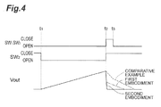
- FIG. 4 is a view illustrating an operation of the photodetecting device 2 according to the second embodiment. This figure shows, in order from the top, the open/close states of the first switch SW 1 and the third switch SW 3 , the open/close state of the second switch SW 2 , and the output voltage value Vout of the photodetecting device 2.
- the first switch SW 1 and the third switch SW 3 are opened. Moreover, before the time t 1 , the second switch SW 2 is closed, the capacitive element C 2 is discharged, and the output voltage value Vout of the photodetecting device 2 is set to an initial value. At the time t 1 , the second switch SW 2 switches from a close state to an open state.
- the integrating circuit 12 inputs an electric charge generated in the photodiode PD to the inverting input terminal P 1 , accumulates the input electric charge into the capacitive element C 2 , and outputs the voltage value Vout according to the amount of accumulated electric charge. Accordingly, the output voltage value Vout of the photodetecting device 2 gradually increases with time.
- the first switch SW 1 , the second switch SW 2 , and the third switch SW 3 switch from the open state to the close state, respectively.
- the capacitive element C 2 continues to be discharged and the output voltage value Vout of the photodetecting device 2 will be set to the initial value.
- the first switch SW 1 and the third switch SW 3 switch to the open state.
- the output voltage value Vout of the photodetecting device 2 at the time t 2 and thereafter is indicated by a solid line for the second embodiment, while it is indicated by a dot-dashed line for the first embodiment, and is indicated by a dashed line for the comparative example.
- the comparative example neither the first switch SW 1 nor the third switch SW 3 is provided.
- the time required for the output voltage value Vout of the photodetecting device at the time t 2 and thereafter to reach the initial value is approximately 3.8 ⁇ s.
- the time required for the output voltage value Vout of the photodetecting device 1 at the time t 2 and thereafter to reach the initial value is approximately 2.1 ⁇ s.
- the time required for the output voltage value Vout of the photodetecting device 2 at the time t 2 and thereafter to reach the initial value is approximately 0.1 ⁇ s.
- the second switch SW 2 switches to the close state and the first switch SW 1 and the third switch SW 3 also switch to the close state, so that the time required for the output voltage value Vout to reach the initial value is shortened further and higher speed can be achieved.
- the reason why the initialization leads to higher speed in the second embodiment is as follows. That is, if at the time t 2 , the second switch SW 2 switches to the close state and the first switch SW 1 also switches to the close state, then the power supply potential VDD is applied to the gate terminal of the PMOS transistor T 1 constituting the driving section to turn off the PMOS transistor T 1 , so that a current will not flow between the source terminal and the drain terminal of the MOS transistor T 1 .
- the current flowing in the NMOS transistor T 2 constituting the driving section does not vary. Accordingly, the electric charge accumulated in the capacitive element C 2 until the time t 2 efficiently flows through the NMOS transistor T 2 .
- the third switch SW 3 also switches to the close state. Accordingly, the electric charge accumulated in the capacitive element C 2 until the time t 2 flows also through the third switch SW 3 .
- the electric charge accumulated in the capacitive element C 2 until the time t 2 efficiently flows not only through the NMOS transistor T 2 , but also through the third switch SW 3 , so that the capacitive element C 2 is more quickly discharged.
- the provision of the first switch SW 1 and the third switch SW 3 makes it possible to achieve both low power consumption and high speed.
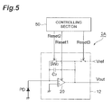
- the third switch SW 3 is provided between the reference potential input terminal to which the reference potential Vref is input and the one terminal of the capacitive element C 2 on the inverting input terminal side of the amplifier circuit 20, but as with a photodetecting device 2A shown in FIG. 5 , the third switch SW 3 may be provided between the reference potential input terminal to which the reference potential Vref is input and one terminal of the capacitive element C 2 on the output terminal side of the amplifier circuit 20.
- the photodetecting device 2A also operates as with the photodetecting device 2 and can attain the same effect as that of the photodetecting device 2.
- the present invention can be used as an amplifier circuit, an integrating circuit, and a photodetecting device capable of achieving both low power consumption and high speed.
Landscapes
- Engineering & Computer Science (AREA)
- Power Engineering (AREA)
- Physics & Mathematics (AREA)
- General Physics & Mathematics (AREA)
- Spectroscopy & Molecular Physics (AREA)
- Amplifiers (AREA)
- Photometry And Measurement Of Optical Pulse Characteristics (AREA)
- Transforming Light Signals Into Electric Signals (AREA)
- Light Receiving Elements (AREA)
Abstract
Description
- The present invention relates to an integrating circuit which accumulates an input electric charge and outputs a voltage value according to the amount of accumulated electric charge, to a photodetecting device including the integrating circuit and a photodiode, and to an amplifier circuit included in the integrating circuit.
- As the photodetecting device, the one including a photodiode and an integrating circuit is known (for example, see Patent Document 1). This integrating circuit includes an amplifier circuit having a first input terminal, a second input terminal, and an output terminal; and a capacitive element and a switch provided between the first input terminal and the output terminal of the amplifier circuit, the capacitive element and the switch being connected in parallel to each other. In this photodetecting device, the switch of the integrating circuit is closed so that the capacitive element in the integrating circuit is discharged, and the voltage value output from the integrating circuit is initialized. When the switch of the integrating circuit is opened, an electric charge generated in the photodiode is accumulated in the capacitive element of the integrating circuit, and a voltage value according to the amount of accumulated electric charge is output from the integrating circuit. Further, if the photodetecting device includes a plurality of photodiodes arranged in one dimension or in two dimensions, it is possible to obtain an optical image in one dimension or in two dimensions.
- Patent Document 1: Japanese Patent Application Laid-Open No.
H06-105067 - In the photodetecting device, there is a need to increase the number of photodiodes arranged, and accordingly, there is also a need to achieve high speed and low power consumption. However, an attempt to reduce the power consumption of the integrating circuit included in the photodetecting device results in a lowering of the drive capability of the amplifier circuit, so that the time required for the output voltage value of the integrating circuit to be initialized by closing the switch of the integrating circuit will increase. That is, conventionally, it is difficult to achieve both low power consumption and high speed.
- The present invention has been made in order to solve the above-described problem, and has an object to provide an amplifier circuit, an integrating circuit, and a photodetecting device capable of achieving both low power consumption and high speed.
- An amplifier circuit according to the present invention has a first input terminal, a second input terminal, and an output terminal, and the amplifier circuit includes (1) a driving section including a PMOS transistor and an NMOS transistor, respective drain terminals thereof being connected to each other, wherein this connection point is connected to the output terminal, and (2) a first switch provided between a first reference potential input terminal to which a first reference potential is input and a gate terminal of the PMOS transistor, the first switch turning off the PMOS transistor by applying the first reference potential to the gate terminal of the PMOS transistor. Note that, of the first input terminal and the second input terminal of the amplifier circuit, one is an inverting input terminal and the other is a non-inverting input terminal.
- An integrating circuit according to the present invention includes (1) the amplifier circuit according to the above-described invention, (2) a capacitive element provided between the first input terminal and the output terminal of the amplifier circuit, and (3) a second switch provided in parallel to the capacitive element between the first input terminal and the output terminal of the amplifier circuit. Preferably, the above-described integrating circuit further includes a third switch provided between a second reference potential input terminal to which a second reference potential is input and one terminal of the capacitive element, the third switch applying the second reference potential to the one terminal of the capacitive element.
- A photodetecting device according to the present invention includes (1) the integrating circuit according to the above-described invention, and (2) a photodiode which generates an amount of electric charge according to an amount of incident light and causes the generated electric charge to enter the first input terminal of the amplifier circuit in the integrating circuit.
- In the present invention, when the second switch is closed in the integrating circuit to discharge the capacitive element and initialize the output voltage value of the integrating circuit, the first switch included in the amplifier circuit is also closed to apply the first reference potential to the gate terminal of the PMOS transistor constituting the driving section of the amplifier circuit and turn off the PMOS transistor. Further, the third switch is also closed to apply the second reference potential to the first input terminal of the amplifier circuit. Thus, the capacitive element in the integrating circuit is quickly discharged.
- According to the present invention, it is possible to achieve both low power consumption and high speed.
-
- [
FIG. 1] FIG. 1 is a view showing a configuration of a photodetecting device 1 according to a first embodiment. - [
FIG. 2] FIG. 2 is a view illustrating an operation of the photodetecting device 1 according to the first embodiment. - [
FIG. 3] FIG. 3 is a view showing a configuration of a photodetectingdevice 2 according to a second embodiment. - [
FIG. 4] FIG. 4 is a view illustrating an operation of the photodetectingdevice 2 according to the second embodiment. - [
FIG. 5] FIG. 5 is a view showing a configuration of a photodetectingdevice 2A according to a modified example of the second embodiment. - Hereinafter, with reference to the accompanying drawings, embodiments of the present invention will be described in detail. In the description of the drawings, the same components are denoted by the same reference symbols, and overlapping description will be omitted.
- (First Embodiment)
-
FIG. 1 is a view showing a configuration of a photodetecting device 1 according to a first embodiment. The photodetecting device 1 shown in this figure includes a photodiode PD and anintegrating circuit 11. The integratingcircuit 11 includes anamplifier circuit 20, a capacitive element C2, and a second switch SW2. - The
amplifier circuit 20 has an inverting input terminal P1, a non-inverting input terminal P2, and an output terminal PO. The capacitive element C2 is provided between the inverting input terminal P1 and the output terminal PO of theamplifier circuit 20. The second switch SW2 is provided in parallel to the capacitive element C2 between the inverting input terminal P1 and the output terminal P0 of theamplifier circuit 20, and is opened or closed according to the level of a second reset signal Reset2. The non-inverting input terminal P2 of theamplifier circuit 20 is connected to a ground potential. Note that, the non-inverting input terminal P2 of theamplifier circuit 20 is not necessarily connected to the ground potential, but may be connected to a potential of 0.1 V or the like, for example, as long as it is connected to a fixed potential. - The photodiode PD has a cathode terminal and an anode terminal, and generates an amount of electric charge according to an amount of incident light. The cathode terminal of the photodiode PD is connected to the inverting input terminal P1 of the
amplifier circuit 20. The anode terminal of the photodiode PD is connected to the ground potential. - The
amplifier circuit 20 has a driving section including a PMOS transistor T1 and an NMOS transistor T2, the respective drain terminals thereof being connected to each other, wherein this connection point is connected to the output terminal P0, The source terminal of the PMOS transistor T1 is connected to a power supply potential VDD. The source terminal of the NMOS transistor T2 is connected to the ground potential. A predetermined DC voltage value VD is input to the gate terminal of the NMOS transistor T2. - Furthermore, the
amplifier circuit 20 includes PMOS transistors T10 to T15, NMOS transistors T16 to T19, and a capacitive element C1. - The source terminal of the PMOS transistor T11 is connected to the power supply potential VDD. A Predetermined DC voltage value VA is input to the gate terminal of the PMOS transistor T11. The drain terminal of the PMOS transistor T11 is connected to the respective source terminals of the PMOS transistors T14 and T15.
- The source terminal of the PMOS transistor T12 is connected to the power supply potential VDD. The gate terminal of the PMOS transistor T12 is connected to the gate terminal of the PMOS transistor T13 and the drain terminal thereof. The drain terminal of the PMOS transistor T12 is connected to the drain terminal of the NMOS transistor T16.
- The source terminal of the PMOS transistor T13 is connected to the power supply potential VDD. The drain terminal of the PMOS transistor T13 is connected to the gate terminal of the PMOS transistor T1 and the drain terminal of the NMOS transistor T17.
- The PMOS transistor T14 and the PMOS transistor T15 constitute a differential pair input section in the
amplifier circuit 20. - The gate terminal of the PMOS transistor T14 is connected to the inverting input terminal P1 of the
amplifier circuit 20. The drain terminal of the PMOS transistor T14 is connected to the source terminal of the NMOS transistor T16 and the drain terminal of the NMOS transistor T18. - The gate terminal of the PMOS transistor T15 is connected to the non-inverting input terminal P2 of the
amplifier circuit 20. The drain terminal of the PMOS transistor T15 is connected to the source terminal of the NMOS transistor T17 and the drain terminal of the NMOS transistor T19, and is also connected to the output terminal PO via the capacitive element C1. - The source terminal of the NMOS transistor T16 is connected to the drain terminal of the NMOS transistor T18. The source terminal of the NMOS transistor T17 is connected to the drain terminal of the NMOS transistor T19. A predetermined DC voltage value VB is input to the respective gate terminals of the NMOS transistor T16 and the NMOS transistor T17,
- The respective source terminals of the NMOS transistor T18 and the NMOS transistor T19 are connected to the ground potential. A predetermined DC voltage value VC is input to the respective gate terminals of the NMOS transistor T18 and the NMOS transistor T19.
- The PMOS transistor T10 functions as a first switch SW1 capable of turning off the PMOS transistor T1 by applying the power supply potential VDD to the gate terminal of the PMOS transistor T1. The first switch SW1 comprising the PMOS transistor T10 is provided between a power supply potential input terminal to which the power supply potential VDD is input and the gate terminal of the PMOS transistor T1.
- The source terminal of the PMOS transistor T10 is connected to the power supply potential input terminal to which the power supply potential VDD is input. The drain terminal of the PMOS transistor T10 is connected to the gate terminal of the PMOS transistor T1. Moreover, a first reset signal Reset1 is input to the gate terminal of the PMOS transistor T10.
- The first switch SW1 configured by the PMOS transistor T10 is opened or closed according to the level of the first reset signal Reset 1 input to the gate terminal. That is, when the first reset signal Tteset1 is at a high level, the first switch SW1 configured by the PMOS transistor T10 is opened. When the first reset signal Reset1 is at a low level, the first switch SW1 configured by the PMOS transistor T10 is closed to apply the power supply potential VDD to the gate terminal of the PMOS transistor T1, thereby turning off the PMOS transistor T1.
- The photodetecting device 1 according to the first embodiment includes a controlling
section 50 controlling the respective open/close operations of the first switch SW1 and the second switch SW2, and operates as follows under the control of this controlling section.FIG. 2 is a view illustrating an operation of the photodetecting device 1. according to the first embodiment. This figure shows, in order from the top, the open/close state of the first switch SW1, the open/close state of the second switch SW2, and an output voltage value Vout of the photodetecting device 1. - Before the time t1, the first switch SW1 comprising the PMOS transistor T10 is opened. Moreover, before the time t1, the second switch SW2 is closed, the capacitive element C2 is discharged, and the output voltage value Vout of the photodetecting device 1 is set to an initial value. At the time t1, the second switch SW2 switches from a close state to an open state.
- During a period from the time t1 to the time t2, the first switch SW1 configured by the PMOS transistor T10 is opened and the second switch SW2 is also opened. During this period, the integrating
circuit 11 inputs an electric charge generated in the photodiode PD to the inverting input terminal P1, accumulates the input electric charge into the capacitive element C2, and outputs the voltage value Vout according to the amount of accumulated electric charge. Accordingly, the output voltage value Vout of the photodetecting device 1 gradually increases with time. - At the time t2, the first switch SW1 configured by the PMOS transistor T10 switches from the open state to the close state, and the second switch SW2 also switches from the open state to the close state. At the time t2 and thereafter, the capacitive element C2 continues to be discharged and the output voltage value Vout of the photodetecting device 1 will be set to the initial value. At the subsequent time t3, the first switch SW1 configured by the PMOS transistor T10 switches to the open state.
- In
FIG. 2 , the output voltage value Vout of the photodetecting device 1 at the time t2 and thereafter is indicated by a solid line for the present embodiment, while it is indicated by a dashed line for a comparative example. In the comparative example, the first switch SW1 comprising the PMOS transistor T10 is not provided. - According to a simulation, in the comparative example in which the first switch SW1 is not provided, the time required for the output voltage value Vout of the photodetecting device at the time t2 and thereafter to reach the initial value is approximately 3.8 µs. In contrast, in the present embodiment in which the first switch SW1 is provided, the time required for the output voltage value Vout of the photodetecting device 1 at the time t2 and thereafter to reach the initial value is approximately 2,1 µs.
- In this manner, in the present embodiment, at the time t2, the second switch SW2 switches to the close state and the first switch SW1 also switches to the close state, so that the time required for the output voltage value Vout to reach the initial value is shortened and high speed can be achieved.
- The reason why the initialization leads to high speed in the present embodiment is as follows. That is, if at the time t2, the second switch SW2 switches to the close state and the first switch SW1 also switches to the close state, then the power supply potential VDD is applied to the gate terminal of the PMOS transistor T1 constituting the driving section to turn off the PMOS transistor T1, so that a current will not flow between the source terminal and the drain terminal of the MOS transistor T1. On the other hand, the current flowing in the NMOS transistor T2 constituting the driving section does not vary.
- Accordingly, the electric charge accumulated in the capacitive element C2 until the time t2 efficiently flows through the NMOS transistor T2, so that the capacitive element C2 is quickly discharged. Generally, an attempt to achieve low power consumption makes it difficult to achieve high speed, but in the present embodiment, the provision of the first switch SW1 makes it possible to achieve both low power consumption and high speed.
- (Second Embodiment)
-
FIG. 3 is a view showing a configuration of aphotodetecting device 2 according to a second embodiment. Thephotodetecting device 2 shown in this figure includes the photodiode PD and an integratingcircuit 12. The integratingcircuit 12 includes theamplifier circuit 20, the capacitive element C2, the second switch SW2, and a third switch SW3. Note that, in thisFIG. 3 , theamplifier circuit 20 is represented by one symbol. - As compared with the configuration of the photodetecting device 1 according to the first embodiment shown in
FIG. 1 , thephotodetecting device 2 according to the second embodiment shown inFIG. 3 differs in that it further includes the third switch SW3. The third switch SW3 is provided between a reference potential input terminal to which a reference potential Vref is input and one terminal (a terminal on the inverting input terminal P1 side of the amplifier circuit 20) of the capacitive element C2, and is opened or closed according to the level of a third reset signal Reset3 and is capable of applying the reference potential Vref to the one terminal of the capacitive element C2. The reference potential Vref may be the ground potential. - The
photodetecting device 2 according to the second embodiment includes the controllingsection 50 controlling the respective open/close operations of the first switch SW1, the second switch SW2, and the third switch SW3, and operates as follows under the control of this controlling section.FIG. 4 is a view illustrating an operation of thephotodetecting device 2 according to the second embodiment. This figure shows, in order from the top, the open/close states of the first switch SW1 and the third switch SW3, the open/close state of the second switch SW2, and the output voltage value Vout of thephotodetecting device 2. - Before the time t1, the first switch SW1 and the third switch SW3 are opened. Moreover, before the time t1, the second switch SW2 is closed, the capacitive element C2 is discharged, and the output voltage value Vout of the
photodetecting device 2 is set to an initial value. At the time t1, the second switch SW2 switches from a close state to an open state. - During the period from the time t1 to the time t2, the first switch SW1, the second switch SW2, and the third switch SW3 are opened, respectively. During this period, the integrating
circuit 12 inputs an electric charge generated in the photodiode PD to the inverting input terminal P1, accumulates the input electric charge into the capacitive element C2, and outputs the voltage value Vout according to the amount of accumulated electric charge. Accordingly, the output voltage value Vout of thephotodetecting device 2 gradually increases with time. - At the time t2, the first switch SW1, the second switch SW2, and the third switch SW3 switch from the open state to the close state, respectively. At the time t2 and thereafter, the capacitive element C2 continues to be discharged and the output voltage value Vout of the
photodetecting device 2 will be set to the initial value. At the subsequent time t3, the first switch SW1 and the third switch SW3 switch to the open state. - In
FIG. 4 , the output voltage value Vout of thephotodetecting device 2 at the time t2 and thereafter is indicated by a solid line for the second embodiment, while it is indicated by a dot-dashed line for the first embodiment, and is indicated by a dashed line for the comparative example. In the comparative example, neither the first switch SW1 nor the third switch SW3 is provided. - According to a simulation, in the comparative example in which the first switch SW1 and the third switch SW3 are not provided, the time required for the output voltage value Vout of the photodetecting device at the time t2 and thereafter to reach the initial value is approximately 3.8 µs. In the first embodiment in which only the first switch SW1 is provided, the time required for the output voltage value Vout of the photodetecting device 1 at the time t2 and thereafter to reach the initial value is approximately 2.1 µs. In contrast, in the second embodiment in which both the first switch SW1 and the third switch SW3 are provided, the time required for the output voltage value Vout of the
photodetecting device 2 at the time t2 and thereafter to reach the initial value is approximately 0.1 µs. - In this manner, in the second embodiment, at the time t2, the second switch SW2 switches to the close state and the first switch SW1 and the third switch SW3 also switch to the close state, so that the time required for the output voltage value Vout to reach the initial value is shortened further and higher speed can be achieved.
- The reason why the initialization leads to higher speed in the second embodiment is as follows. That is, if at the time t2, the second switch SW2 switches to the close state and the first switch SW1 also switches to the close state, then the power supply potential VDD is applied to the gate terminal of the PMOS transistor T1 constituting the driving section to turn off the PMOS transistor T1, so that a current will not flow between the source terminal and the drain terminal of the MOS transistor T1. On the other hand, the current flowing in the NMOS transistor T2 constituting the driving section does not vary. Accordingly, the electric charge accumulated in the capacitive element C2 until the time t2 efficiently flows through the NMOS transistor T2. Moreover, in the second embodiment, at the time t2, the third switch SW3 also switches to the close state. Accordingly, the electric charge accumulated in the capacitive element C2 until the time t2 flows also through the third switch SW3.
- In this manner, in the second embodiment, the electric charge accumulated in the capacitive element C2 until the time t2 efficiently flows not only through the NMOS transistor T2, but also through the third switch SW3, so that the capacitive element C2 is more quickly discharged. Generally, an attempt to achieve low power consumption makes it difficult to achieve high speed, but in the second embodiment, the provision of the first switch SW1 and the third switch SW3 makes it possible to achieve both low power consumption and high speed.
- Note that, in the
photodetecting device 2 according to the second embodiment, the third switch SW3 is provided between the reference potential input terminal to which the reference potential Vref is input and the one terminal of the capacitive element C2 on the inverting input terminal side of theamplifier circuit 20, but as with aphotodetecting device 2A shown inFIG. 5 , the third switch SW3 may be provided between the reference potential input terminal to which the reference potential Vref is input and one terminal of the capacitive element C2 on the output terminal side of theamplifier circuit 20. Thephotodetecting device 2A also operates as with thephotodetecting device 2 and can attain the same effect as that of thephotodetecting device 2. - The present invention can be used as an amplifier circuit, an integrating circuit, and a photodetecting device capable of achieving both low power consumption and high speed.
- 1, 2, 2A - photodetecting device, 11, 12 - integrating circuit, 20 - amplifier circuit, SW1 - first switch, SW2 - second switch, SW3 - third switch, C1, C2 - capacitive element, PD - photodiode, T1, T10 to T15 - PMOS transistor, T2, T16 to T19 - NMOS transistor, 50 - controlling section.
Claims (4)
- An amplifier circuit having a first input terminal a second input terminal, and an output terminal, the amplifier circuit comprising:a driving section including a PMOS transistor and an NMOS transistor, respective drain terminals thereof being connected to each other, wherein this connection point is connected to the output terminal; anda first switch provided between a first reference potential input terminal to which a first reference potential is input and a gate terminal of the PMOS transistor, the first switch turning off the PMOS transistor by applying the first reference potential to the gate terminal of the PMOS transistor.
- An integrating circuit, comprising:the amplifier circuit according to claim 1;a capacitive element provided between the first input terminal and the output terminal of the amplifier circuit; anda second switch provided in parallel to the capacitive element between the first input terminal and the output terminal of the amplifier circuit.
- The integrating circuit according to claim 2, further comprising a third switch provided between a second reference potential input terminal to which a second reference potential is input and one terminal of the capacitive element, the third switch applying the second reference potential to the one terminal of the capacitive element.
- A photodetecting device, comprising:the integrating circuit according to claim 2 or 3; anda photodiode which generates an amount of electric charge according to an amount of incident light and causes the generated electric charge to enter the first input terminal of the amplifier circuit in the integrating circuit.
Applications Claiming Priority (2)
| Application Number | Priority Date | Filing Date | Title |
|---|---|---|---|
| JP2009147620A JP5296612B2 (en) | 2009-06-22 | 2009-06-22 | Integration circuit and photodetector |
| PCT/JP2010/059838 WO2010150658A1 (en) | 2009-06-22 | 2010-06-10 | Amplifier circuit, integrating circuit, and light-detection device |
Publications (3)
| Publication Number | Publication Date |
|---|---|
| EP2448116A1 true EP2448116A1 (en) | 2012-05-02 |
| EP2448116A4 EP2448116A4 (en) | 2012-12-26 |
| EP2448116B1 EP2448116B1 (en) | 2019-01-16 |
Family
ID=43386430
Family Applications (1)
| Application Number | Title | Priority Date | Filing Date |
|---|---|---|---|
| EP10791976.3A Active EP2448116B1 (en) | 2009-06-22 | 2010-06-10 | Amplifier circuit, integrating circuit, and light-detection device |
Country Status (7)
| Country | Link |
|---|---|
| US (1) | US8717105B2 (en) |
| EP (1) | EP2448116B1 (en) |
| JP (1) | JP5296612B2 (en) |
| KR (1) | KR101721271B1 (en) |
| CN (1) | CN102460963B (en) |
| TW (1) | TWI521863B (en) |
| WO (1) | WO2010150658A1 (en) |
Cited By (1)
| Publication number | Priority date | Publication date | Assignee | Title |
|---|---|---|---|---|
| EP2448113A4 (en) * | 2009-06-22 | 2014-12-24 | Hamamatsu Photonics Kk | Integrating circuit and light-detection device |
Families Citing this family (1)
| Publication number | Priority date | Publication date | Assignee | Title |
|---|---|---|---|---|
| JP5973832B2 (en) | 2012-08-02 | 2016-08-23 | 株式会社堀場製作所 | Amplifier and radiation detector |
Family Cites Families (14)
| Publication number | Priority date | Publication date | Assignee | Title |
|---|---|---|---|---|
| US4988954A (en) * | 1989-04-28 | 1991-01-29 | Crystal Semiconductor Corporation | Low power output stage circuitry in an amplifier |
| JP3302030B2 (en) * | 1990-10-09 | 2002-07-15 | 株式会社東芝 | Buffer circuit |
| JP2728832B2 (en) | 1992-09-18 | 1998-03-18 | 浜松ホトニクス株式会社 | Image reading device |
| US5363059A (en) * | 1993-06-17 | 1994-11-08 | Texas Instruments Incorporated | Transconductance amplifier |
| US6107883A (en) * | 1998-09-10 | 2000-08-22 | Seiko Epson Corporation | High gain, high speed rail-to-rail amplifier |
| CN1194469C (en) * | 2001-12-28 | 2005-03-23 | 北京六合万通微电子技术有限公司 | Low power consumption analogue signal sample retaining circuit and its application method |
| CN100525400C (en) * | 2002-11-07 | 2009-08-05 | 克塞尼克斯股份有限公司 | Read-out circuit for infrared detectors |
| JP4356816B2 (en) | 2005-03-09 | 2009-11-04 | 三菱農機株式会社 | Transplanter |
| JP2007036653A (en) | 2005-07-27 | 2007-02-08 | Oki Electric Ind Co Ltd | Operational amplifier and constant current generating circuit using it |
| JP2007104358A (en) * | 2005-10-05 | 2007-04-19 | Matsushita Electric Ind Co Ltd | CMOS amplifier |
| JP2008029098A (en) * | 2006-07-20 | 2008-02-07 | Oki Electric Ind Co Ltd | Voltage booster circuit |
| JP2008092272A (en) * | 2006-10-02 | 2008-04-17 | New Japan Radio Co Ltd | Amplifier circuit |
| KR20090015249A (en) * | 2007-08-08 | 2009-02-12 | 삼성전자주식회사 | A differential amplifier, and a method of amplifying signals of the differential amplifier, and a display driving device including the differential amplifier |
| JP4661876B2 (en) * | 2008-01-18 | 2011-03-30 | ソニー株式会社 | Solid-state imaging device and camera system |
-
2009
- 2009-06-22 JP JP2009147620A patent/JP5296612B2/en active Active
-
2010
- 2010-06-10 KR KR1020117022670A patent/KR101721271B1/en active Active
- 2010-06-10 EP EP10791976.3A patent/EP2448116B1/en active Active
- 2010-06-10 CN CN201080027821.4A patent/CN102460963B/en active Active
- 2010-06-10 WO PCT/JP2010/059838 patent/WO2010150658A1/en not_active Ceased
- 2010-06-10 US US13/379,126 patent/US8717105B2/en active Active
- 2010-06-17 TW TW099119738A patent/TWI521863B/en active
Cited By (1)
| Publication number | Priority date | Publication date | Assignee | Title |
|---|---|---|---|---|
| EP2448113A4 (en) * | 2009-06-22 | 2014-12-24 | Hamamatsu Photonics Kk | Integrating circuit and light-detection device |
Also Published As
| Publication number | Publication date |
|---|---|
| CN102460963B (en) | 2015-03-25 |
| US8717105B2 (en) | 2014-05-06 |
| KR20120036798A (en) | 2012-04-18 |
| EP2448116B1 (en) | 2019-01-16 |
| WO2010150658A1 (en) | 2010-12-29 |
| JP5296612B2 (en) | 2013-09-25 |
| TWI521863B (en) | 2016-02-11 |
| EP2448116A4 (en) | 2012-12-26 |
| KR101721271B1 (en) | 2017-03-29 |
| CN102460963A (en) | 2012-05-16 |
| JP2011004326A (en) | 2011-01-06 |
| US20130038393A1 (en) | 2013-02-14 |
| TW201123712A (en) | 2011-07-01 |
Similar Documents
| Publication | Publication Date | Title |
|---|---|---|
| JP5305519B2 (en) | Voltage regulator circuit | |
| JP4901445B2 (en) | Drive circuit and semiconductor device using the same | |
| US9397653B2 (en) | Semiconductor device | |
| EP2448113A1 (en) | Integrating circuit and light-detection device | |
| KR20100088086A (en) | Power-on reset circuit | |
| EP3267583B1 (en) | Circuit for selecting a supply voltage with controlled transition | |
| US8717105B2 (en) | Amplifier circuit, integrating circuit, and light-detection device | |
| JP4229804B2 (en) | Semiconductor output circuit | |
| JP5723303B2 (en) | Light receiving circuit | |
| US6518804B2 (en) | Semiconductor integrated circuit device | |
| JP2010124083A (en) | Bootstrap circuit | |
| US9285269B2 (en) | Light receiving circuit | |
| WO2006029286A1 (en) | Low-voltage cmos switch with novel clock boosting scheme | |
| JP5702357B2 (en) | Bootstrap switch circuit | |
| US20080007299A1 (en) | Power generation circuit | |
| JP5671916B2 (en) | Shift register | |
| CN110784221A (en) | Design method for preventing AD sampling channel from electric leakage | |
| US9503078B1 (en) | Method and apparatus for charge transfer | |
| JP2005244506A (en) | Amplifier circuit, integration circuit, and photodetector | |
| JP2013258490A (en) | Voltage conversion circuit, charge pump circuit, and dc/dc converter | |
| JP2004215018A (en) | Pull-down circuit, pull-up circuit and CMOS integrated circuit | |
| JP2003218684A (en) | Malfunction prevention circuit | |
| JP2007129307A (en) | Power supply circuit and matrix substrate using the same | |
| JP2005283458A (en) | Voltage detection circuit | |
| JP2010193688A (en) | Boosting circuit |
Legal Events
| Date | Code | Title | Description |
|---|---|---|---|
| PUAI | Public reference made under article 153(3) epc to a published international application that has entered the european phase |
Free format text: ORIGINAL CODE: 0009012 |
|
| 17P | Request for examination filed |
Effective date: 20120117 |
|
| AK | Designated contracting states |
Kind code of ref document: A1 Designated state(s): AL AT BE BG CH CY CZ DE DK EE ES FI FR GB GR HR HU IE IS IT LI LT LU LV MC MK MT NL NO PL PT RO SE SI SK SM TR |
|
| DAX | Request for extension of the european patent (deleted) | ||
| A4 | Supplementary search report drawn up and despatched |
Effective date: 20121122 |
|
| RIC1 | Information provided on ipc code assigned before grant |
Ipc: H03F 3/45 20060101ALI20121116BHEP Ipc: H03F 3/08 20060101ALI20121116BHEP Ipc: H03F 3/30 20060101AFI20121116BHEP Ipc: H04N 5/33 20060101ALI20121116BHEP Ipc: H04N 5/365 20110101ALI20121116BHEP Ipc: G01J 1/44 20060101ALI20121116BHEP Ipc: G01J 1/46 20060101ALI20121116BHEP Ipc: H03F 1/02 20060101ALI20121116BHEP |
|
| STAA | Information on the status of an ep patent application or granted ep patent |
Free format text: STATUS: EXAMINATION IS IN PROGRESS |
|
| 17Q | First examination report despatched |
Effective date: 20171222 |
|
| GRAP | Despatch of communication of intention to grant a patent |
Free format text: ORIGINAL CODE: EPIDOSNIGR1 |
|
| STAA | Information on the status of an ep patent application or granted ep patent |
Free format text: STATUS: GRANT OF PATENT IS INTENDED |
|
| INTG | Intention to grant announced |
Effective date: 20180914 |
|
| RIN1 | Information on inventor provided before grant (corrected) |
Inventor name: ITO, SHINYA Inventor name: FUNAKOSHI, HARUHIRO |
|
| GRAS | Grant fee paid |
Free format text: ORIGINAL CODE: EPIDOSNIGR3 |
|
| GRAA | (expected) grant |
Free format text: ORIGINAL CODE: 0009210 |
|
| STAA | Information on the status of an ep patent application or granted ep patent |
Free format text: STATUS: THE PATENT HAS BEEN GRANTED |
|
| AK | Designated contracting states |
Kind code of ref document: B1 Designated state(s): AL AT BE BG CH CY CZ DE DK EE ES FI FR GB GR HR HU IE IS IT LI LT LU LV MC MK MT NL NO PL PT RO SE SI SK SM TR |
|
| REG | Reference to a national code |
Ref country code: GB Ref legal event code: FG4D |
|
| REG | Reference to a national code |
Ref country code: CH Ref legal event code: EP |
|
| REG | Reference to a national code |
Ref country code: IE Ref legal event code: FG4D |
|
| REG | Reference to a national code |
Ref country code: DE Ref legal event code: R096 Ref document number: 602010056621 Country of ref document: DE |
|
| REG | Reference to a national code |
Ref country code: AT Ref legal event code: REF Ref document number: 1090473 Country of ref document: AT Kind code of ref document: T Effective date: 20190215 |
|
| REG | Reference to a national code |
Ref country code: NL Ref legal event code: MP Effective date: 20190116 |
|
| REG | Reference to a national code |
Ref country code: LT Ref legal event code: MG4D |
|
| PG25 | Lapsed in a contracting state [announced via postgrant information from national office to epo] |
Ref country code: NL Free format text: LAPSE BECAUSE OF FAILURE TO SUBMIT A TRANSLATION OF THE DESCRIPTION OR TO PAY THE FEE WITHIN THE PRESCRIBED TIME-LIMIT Effective date: 20190116 |
|
| REG | Reference to a national code |
Ref country code: AT Ref legal event code: MK05 Ref document number: 1090473 Country of ref document: AT Kind code of ref document: T Effective date: 20190116 |
|
| PG25 | Lapsed in a contracting state [announced via postgrant information from national office to epo] |
Ref country code: PT Free format text: LAPSE BECAUSE OF FAILURE TO SUBMIT A TRANSLATION OF THE DESCRIPTION OR TO PAY THE FEE WITHIN THE PRESCRIBED TIME-LIMIT Effective date: 20190516 Ref country code: NO Free format text: LAPSE BECAUSE OF FAILURE TO SUBMIT A TRANSLATION OF THE DESCRIPTION OR TO PAY THE FEE WITHIN THE PRESCRIBED TIME-LIMIT Effective date: 20190416 Ref country code: ES Free format text: LAPSE BECAUSE OF FAILURE TO SUBMIT A TRANSLATION OF THE DESCRIPTION OR TO PAY THE FEE WITHIN THE PRESCRIBED TIME-LIMIT Effective date: 20190116 Ref country code: PL Free format text: LAPSE BECAUSE OF FAILURE TO SUBMIT A TRANSLATION OF THE DESCRIPTION OR TO PAY THE FEE WITHIN THE PRESCRIBED TIME-LIMIT Effective date: 20190116 Ref country code: LT Free format text: LAPSE BECAUSE OF FAILURE TO SUBMIT A TRANSLATION OF THE DESCRIPTION OR TO PAY THE FEE WITHIN THE PRESCRIBED TIME-LIMIT Effective date: 20190116 Ref country code: SE Free format text: LAPSE BECAUSE OF FAILURE TO SUBMIT A TRANSLATION OF THE DESCRIPTION OR TO PAY THE FEE WITHIN THE PRESCRIBED TIME-LIMIT Effective date: 20190116 Ref country code: FI Free format text: LAPSE BECAUSE OF FAILURE TO SUBMIT A TRANSLATION OF THE DESCRIPTION OR TO PAY THE FEE WITHIN THE PRESCRIBED TIME-LIMIT Effective date: 20190116 |
|
| PG25 | Lapsed in a contracting state [announced via postgrant information from national office to epo] |
Ref country code: BG Free format text: LAPSE BECAUSE OF FAILURE TO SUBMIT A TRANSLATION OF THE DESCRIPTION OR TO PAY THE FEE WITHIN THE PRESCRIBED TIME-LIMIT Effective date: 20190416 Ref country code: LV Free format text: LAPSE BECAUSE OF FAILURE TO SUBMIT A TRANSLATION OF THE DESCRIPTION OR TO PAY THE FEE WITHIN THE PRESCRIBED TIME-LIMIT Effective date: 20190116 Ref country code: IS Free format text: LAPSE BECAUSE OF FAILURE TO SUBMIT A TRANSLATION OF THE DESCRIPTION OR TO PAY THE FEE WITHIN THE PRESCRIBED TIME-LIMIT Effective date: 20190516 Ref country code: GR Free format text: LAPSE BECAUSE OF FAILURE TO SUBMIT A TRANSLATION OF THE DESCRIPTION OR TO PAY THE FEE WITHIN THE PRESCRIBED TIME-LIMIT Effective date: 20190417 Ref country code: HR Free format text: LAPSE BECAUSE OF FAILURE TO SUBMIT A TRANSLATION OF THE DESCRIPTION OR TO PAY THE FEE WITHIN THE PRESCRIBED TIME-LIMIT Effective date: 20190116 |
|
| REG | Reference to a national code |
Ref country code: DE Ref legal event code: R097 Ref document number: 602010056621 Country of ref document: DE |
|
| PG25 | Lapsed in a contracting state [announced via postgrant information from national office to epo] |
Ref country code: EE Free format text: LAPSE BECAUSE OF FAILURE TO SUBMIT A TRANSLATION OF THE DESCRIPTION OR TO PAY THE FEE WITHIN THE PRESCRIBED TIME-LIMIT Effective date: 20190116 Ref country code: DK Free format text: LAPSE BECAUSE OF FAILURE TO SUBMIT A TRANSLATION OF THE DESCRIPTION OR TO PAY THE FEE WITHIN THE PRESCRIBED TIME-LIMIT Effective date: 20190116 Ref country code: SK Free format text: LAPSE BECAUSE OF FAILURE TO SUBMIT A TRANSLATION OF THE DESCRIPTION OR TO PAY THE FEE WITHIN THE PRESCRIBED TIME-LIMIT Effective date: 20190116 Ref country code: AL Free format text: LAPSE BECAUSE OF FAILURE TO SUBMIT A TRANSLATION OF THE DESCRIPTION OR TO PAY THE FEE WITHIN THE PRESCRIBED TIME-LIMIT Effective date: 20190116 Ref country code: CZ Free format text: LAPSE BECAUSE OF FAILURE TO SUBMIT A TRANSLATION OF THE DESCRIPTION OR TO PAY THE FEE WITHIN THE PRESCRIBED TIME-LIMIT Effective date: 20190116 Ref country code: AT Free format text: LAPSE BECAUSE OF FAILURE TO SUBMIT A TRANSLATION OF THE DESCRIPTION OR TO PAY THE FEE WITHIN THE PRESCRIBED TIME-LIMIT Effective date: 20190116 Ref country code: RO Free format text: LAPSE BECAUSE OF FAILURE TO SUBMIT A TRANSLATION OF THE DESCRIPTION OR TO PAY THE FEE WITHIN THE PRESCRIBED TIME-LIMIT Effective date: 20190116 |
|
| PLBE | No opposition filed within time limit |
Free format text: ORIGINAL CODE: 0009261 |
|
| STAA | Information on the status of an ep patent application or granted ep patent |
Free format text: STATUS: NO OPPOSITION FILED WITHIN TIME LIMIT |
|
| PG25 | Lapsed in a contracting state [announced via postgrant information from national office to epo] |
Ref country code: SM Free format text: LAPSE BECAUSE OF FAILURE TO SUBMIT A TRANSLATION OF THE DESCRIPTION OR TO PAY THE FEE WITHIN THE PRESCRIBED TIME-LIMIT Effective date: 20190116 |
|
| 26N | No opposition filed |
Effective date: 20191017 |
|
| PG25 | Lapsed in a contracting state [announced via postgrant information from national office to epo] |
Ref country code: MC Free format text: LAPSE BECAUSE OF FAILURE TO SUBMIT A TRANSLATION OF THE DESCRIPTION OR TO PAY THE FEE WITHIN THE PRESCRIBED TIME-LIMIT Effective date: 20190116 |
|
| REG | Reference to a national code |
Ref country code: CH Ref legal event code: PL |
|
| PG25 | Lapsed in a contracting state [announced via postgrant information from national office to epo] |
Ref country code: SI Free format text: LAPSE BECAUSE OF FAILURE TO SUBMIT A TRANSLATION OF THE DESCRIPTION OR TO PAY THE FEE WITHIN THE PRESCRIBED TIME-LIMIT Effective date: 20190116 |
|
| REG | Reference to a national code |
Ref country code: BE Ref legal event code: MM Effective date: 20190630 |
|
| PG25 | Lapsed in a contracting state [announced via postgrant information from national office to epo] |
Ref country code: TR Free format text: LAPSE BECAUSE OF FAILURE TO SUBMIT A TRANSLATION OF THE DESCRIPTION OR TO PAY THE FEE WITHIN THE PRESCRIBED TIME-LIMIT Effective date: 20190116 |
|
| PG25 | Lapsed in a contracting state [announced via postgrant information from national office to epo] |
Ref country code: IE Free format text: LAPSE BECAUSE OF NON-PAYMENT OF DUE FEES Effective date: 20190610 |
|
| PG25 | Lapsed in a contracting state [announced via postgrant information from national office to epo] |
Ref country code: BE Free format text: LAPSE BECAUSE OF NON-PAYMENT OF DUE FEES Effective date: 20190630 Ref country code: LI Free format text: LAPSE BECAUSE OF NON-PAYMENT OF DUE FEES Effective date: 20190630 Ref country code: CH Free format text: LAPSE BECAUSE OF NON-PAYMENT OF DUE FEES Effective date: 20190630 Ref country code: LU Free format text: LAPSE BECAUSE OF NON-PAYMENT OF DUE FEES Effective date: 20190610 |
|
| PG25 | Lapsed in a contracting state [announced via postgrant information from national office to epo] |
Ref country code: CY Free format text: LAPSE BECAUSE OF FAILURE TO SUBMIT A TRANSLATION OF THE DESCRIPTION OR TO PAY THE FEE WITHIN THE PRESCRIBED TIME-LIMIT Effective date: 20190116 |
|
| PG25 | Lapsed in a contracting state [announced via postgrant information from national office to epo] |
Ref country code: MT Free format text: LAPSE BECAUSE OF FAILURE TO SUBMIT A TRANSLATION OF THE DESCRIPTION OR TO PAY THE FEE WITHIN THE PRESCRIBED TIME-LIMIT Effective date: 20190116 Ref country code: HU Free format text: LAPSE BECAUSE OF FAILURE TO SUBMIT A TRANSLATION OF THE DESCRIPTION OR TO PAY THE FEE WITHIN THE PRESCRIBED TIME-LIMIT; INVALID AB INITIO Effective date: 20100610 |
|
| PG25 | Lapsed in a contracting state [announced via postgrant information from national office to epo] |
Ref country code: MK Free format text: LAPSE BECAUSE OF FAILURE TO SUBMIT A TRANSLATION OF THE DESCRIPTION OR TO PAY THE FEE WITHIN THE PRESCRIBED TIME-LIMIT Effective date: 20190116 |
|
| P01 | Opt-out of the competence of the unified patent court (upc) registered |
Effective date: 20230509 |
|
| PGFP | Annual fee paid to national office [announced via postgrant information from national office to epo] |
Ref country code: DE Payment date: 20250429 Year of fee payment: 16 |
|
| PGFP | Annual fee paid to national office [announced via postgrant information from national office to epo] |
Ref country code: GB Payment date: 20250501 Year of fee payment: 16 |
|
| PGFP | Annual fee paid to national office [announced via postgrant information from national office to epo] |
Ref country code: IT Payment date: 20250522 Year of fee payment: 16 |
|
| PGFP | Annual fee paid to national office [announced via postgrant information from national office to epo] |
Ref country code: FR Payment date: 20250508 Year of fee payment: 16 |