EP2448034A2 - Organic light emitting device and method for manufacturing the same - Google Patents
Organic light emitting device and method for manufacturing the same Download PDFInfo
- Publication number
- EP2448034A2 EP2448034A2 EP11186648A EP11186648A EP2448034A2 EP 2448034 A2 EP2448034 A2 EP 2448034A2 EP 11186648 A EP11186648 A EP 11186648A EP 11186648 A EP11186648 A EP 11186648A EP 2448034 A2 EP2448034 A2 EP 2448034A2
- Authority
- EP
- European Patent Office
- Prior art keywords
- layer
- emission layer
- light emitting
- emitting device
- organic light
- Prior art date
- Legal status (The legal status is an assumption and is not a legal conclusion. Google has not performed a legal analysis and makes no representation as to the accuracy of the status listed.)
- Granted
Links
Images

Classifications
-
- H—ELECTRICITY
- H10—SEMICONDUCTOR DEVICES; ELECTRIC SOLID-STATE DEVICES NOT OTHERWISE PROVIDED FOR
- H10K—ORGANIC ELECTRIC SOLID-STATE DEVICES
- H10K50/00—Organic light-emitting devices
- H10K50/10—OLEDs or polymer light-emitting diodes [PLED]
- H10K50/11—OLEDs or polymer light-emitting diodes [PLED] characterised by the electroluminescent [EL] layers
- H10K50/125—OLEDs or polymer light-emitting diodes [PLED] characterised by the electroluminescent [EL] layers specially adapted for multicolour light emission, e.g. for emitting white light
- H10K50/13—OLEDs or polymer light-emitting diodes [PLED] characterised by the electroluminescent [EL] layers specially adapted for multicolour light emission, e.g. for emitting white light comprising stacked EL layers within one EL unit
-
- H—ELECTRICITY
- H10—SEMICONDUCTOR DEVICES; ELECTRIC SOLID-STATE DEVICES NOT OTHERWISE PROVIDED FOR
- H10K—ORGANIC ELECTRIC SOLID-STATE DEVICES
- H10K71/00—Manufacture or treatment specially adapted for the organic devices covered by this subclass
- H10K71/10—Deposition of organic active material
- H10K71/12—Deposition of organic active material using liquid deposition, e.g. spin coating
-
- H—ELECTRICITY
- H10—SEMICONDUCTOR DEVICES; ELECTRIC SOLID-STATE DEVICES NOT OTHERWISE PROVIDED FOR
- H10K—ORGANIC ELECTRIC SOLID-STATE DEVICES
- H10K50/00—Organic light-emitting devices
- H10K50/10—OLEDs or polymer light-emitting diodes [PLED]
- H10K50/11—OLEDs or polymer light-emitting diodes [PLED] characterised by the electroluminescent [EL] layers
-
- H—ELECTRICITY
- H10—SEMICONDUCTOR DEVICES; ELECTRIC SOLID-STATE DEVICES NOT OTHERWISE PROVIDED FOR
- H10K—ORGANIC ELECTRIC SOLID-STATE DEVICES
- H10K50/00—Organic light-emitting devices
- H10K50/10—OLEDs or polymer light-emitting diodes [PLED]
- H10K50/14—Carrier transporting layers
- H10K50/15—Hole transporting layers
-
- H—ELECTRICITY
- H10—SEMICONDUCTOR DEVICES; ELECTRIC SOLID-STATE DEVICES NOT OTHERWISE PROVIDED FOR
- H10K—ORGANIC ELECTRIC SOLID-STATE DEVICES
- H10K50/00—Organic light-emitting devices
- H10K50/80—Constructional details
- H10K50/84—Passivation; Containers; Encapsulations
-
- H—ELECTRICITY
- H10—SEMICONDUCTOR DEVICES; ELECTRIC SOLID-STATE DEVICES NOT OTHERWISE PROVIDED FOR
- H10K—ORGANIC ELECTRIC SOLID-STATE DEVICES
- H10K2101/00—Properties of the organic materials covered by group H10K85/00
- H10K2101/10—Triplet emission
-
- H—ELECTRICITY
- H10—SEMICONDUCTOR DEVICES; ELECTRIC SOLID-STATE DEVICES NOT OTHERWISE PROVIDED FOR
- H10K—ORGANIC ELECTRIC SOLID-STATE DEVICES
- H10K2102/00—Constructional details relating to the organic devices covered by this subclass
- H10K2102/301—Details of OLEDs
- H10K2102/361—Temperature
-
- H—ELECTRICITY
- H10—SEMICONDUCTOR DEVICES; ELECTRIC SOLID-STATE DEVICES NOT OTHERWISE PROVIDED FOR
- H10K—ORGANIC ELECTRIC SOLID-STATE DEVICES
- H10K50/00—Organic light-emitting devices
- H10K50/80—Constructional details
- H10K50/84—Passivation; Containers; Encapsulations
- H10K50/844—Encapsulations
-
- H—ELECTRICITY
- H10—SEMICONDUCTOR DEVICES; ELECTRIC SOLID-STATE DEVICES NOT OTHERWISE PROVIDED FOR
- H10K—ORGANIC ELECTRIC SOLID-STATE DEVICES
- H10K71/00—Manufacture or treatment specially adapted for the organic devices covered by this subclass
Definitions
- This document relates to an organic light emitting device and a method for manufacturing the same, and more particularly, to an organic light emitting device, which can improve interfacial characteristics between a first electrode and an organic layer or between organic layers, and a method for manufacturing the same.
- a flat panel display With the development of multimedia, a flat panel display (FPD) is recently becoming more important.
- FPD flat panel display
- LCD liquid crystal display
- PDP plasma display panel
- FED field emitting display
- organic light emitting device an organic light emitting device
- the OLED is a self-emitting type which has a high-speed response speed (i.e., a response speed of 1 ms or less) and low consumption power.
- the OLED is also advantageous as a motion image display medium irrespective of the size of the device because it has no problem in the viewing angle.
- the OLED is being in the spotlight as the next-generation FPD because the OLED can be fabricated at low temperature and has a simple manufacturing process based on the existing semiconductor process technology.
- the OLED comprises a first electrode, a second electrode, and a light emitting layer disposed between the first electrode and the second electrode. Holes supplied from the first electrode and electrons supplied from the second electrode bond together in the light emitting layer to form excitons, and the OLED emits light due to energy generated when the excitons return to the bottom level.
- An organic light emitting device comprises: a substrate; a first electrode disposed on the substrate; a hole function layer disposed on the first electrode; a first emission layer disposed on the hole function layer; a second emission layer disposed on the first emission layer; an electron function layer disposed on the second emission layer; and a second electrode disposed on the electron function layer, wherein the hole function layer and the first emission layer are melted.
- a method for manufacturing an organic light emitting device comprises: forming a first electrode disposed on a substrate; forming a hole function layer on the first electrode; forming a first emission layer on the hole function layer; melting the hole function layer and the first emission layer; forming a second emission layer on the first emission layer; forming an electron function layer on the second emission layer; and forming a second electrode on the electron function layer.
- FIG. 1 is a view showing an organic light emitting device according to an exemplary embodiment of the present invention.
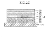
- FIGS. 2A to 2C are views showing the respective steps in a manufacturing method of the organic light emitting device according to an exemplary embodiment of the present invention.
- FIG. 1 is a view showing an organic light emitting device according to an exemplary embodiment of the present invention.
- the organic light emitting device 100 comprises a substrate 110, a first electrode 120, a hole function layer 130, an emission layer 140 comprising a first emission layer 141 and a second emission layer 142, an electron transportation layer 150, an electron injection layer 160, and a second electrode 170.
- the substrate 110 may be made of glass, plastic, or metal, and may further comprise a thin film transistor comprising a semiconductor layer, a gate electrode, a source electrode, and a drain electrode.
- the first electrode 120 may be transparent or reflective. If the first electrode 120 is transparent, it may be made of any one of indium tin oxide (ITO), indium zinc oxide (IZO), and zinc oxide (ZnO).
- ITO indium tin oxide
- IZO indium zinc oxide
- ZnO zinc oxide
- the first electrode 120 may further comprise a reflection layer, made of any one of aluminum (Al), silver (Ag), and nickel (Ni), placed under a layer made of any one of ITO, IZO and, ZnO, or further may comprise a reflection layer interposed between two layers made of any one of ITO, IZO and ZnO.
- a reflection layer made of any one of aluminum (Al), silver (Ag), and nickel (Ni) placed under a layer made of any one of ITO, IZO and, ZnO, or further may comprise a reflection layer interposed between two layers made of any one of ITO, IZO and ZnO.
- the hole function layer 130 functions to make smooth the injection and transportation of holes from the first electrode 120 to the emission layer 140, and may comprise a hole injection layer and a hole transportation layer.
- the hole injection layer may be made of at least one selected from the group consisting of CuPC (cupper phthalocyanine), PEDOT (poly(3,4)-ethylenedioxythiophene), PANI (polyalniline), and NPD (N,N-dinaphthyl-N,N'-diphenyl benzidine), but not limited thereto.
- CuPC cupper phthalocyanine
- PEDOT poly(3,4)-ethylenedioxythiophene
- PANI polyalniline
- NPD N,N-dinaphthyl-N,N'-diphenyl benzidine
- the hole transportation layer may be made of at least one selected from the group consisting of NPD (N,N-dinaphthyl-N,N'-diphenyl benzidine), TPD (N,N'-bis-(3-methylphenyl)-N,N'-bis-(phenyl)-benzidine), s-TAD and MTDATA (4,4',4"-Tris(N-3-methylphenyl-N-phenyl-amino)-triphenylamine), but not limited thereto.
- NPD N,N-dinaphthyl-N,N'-diphenyl benzidine
- TPD N,N'-bis-(3-methylphenyl)-N,N'-bis-(phenyl)-benzidine
- s-TAD and MTDATA (4,4',4"-Tris(N-3-methylphenyl-N-phenyl-amino)-triphenylamine
- the emission layer 140 may comprise a first emission layer 141 and a second emission layer 142.
- the first emission layer 141 is a layer contacting the hole function layer 130, and may comprise a single host material.
- the host material is determined according to the light emission color of the second emission layer 142, which will be described below.
- the second emission layer 142 disposed on the first emission layer 141 may comprise a host and a dopant.
- the second emission layer 142 may comprise a region comprising a light emitting dopant for directly emitting light.
- the second emission layer 142 may be made of a material emitting light of any one of red, green, and blue, or of a phosphorescent material or a fluorescent material.
- the second emission layer 142 is a red light emitting layer, it may be made of a phosphorescent material which comprises a host material comprising CBP (carbazole biphenyl) or mCP(1,3-bis(carbazol-9-yl) and a dopant comprising any one or more selected from the group consisting of PIQIr(acac)(bis(1-phenylisoquinoline)acetylacetonate iridium), PQIr(acac)(bis(1-phenylquinoline)acetylacetonate iridium), PQIr(tris(1-phenylquinoline)iridium), and PtOEP(octaethylporphyrin platinum).
- a fluorescent material comprising PBD:Eu(DBM)3(Phen) or Perylene, but not limited thereto.
- the second emission layer 142 is a green light emitting layer, it may be made of a phosphorescent material which comprises a host material comprising CBP or mCP and a dopant material comprising Ir(ppy)3(fac tris(2-phenylpyridine)iridium). Alternatively, it may be made of a fluorescent material comprising Alq3(tris(8-hydroxyquinolino)aluminum, but not limited thereto.
- the second emission layer 142 is a blue light emitting layer, it may be made of a phosphorescent material which comprises a host material comprising CBP or mCP and a dopant material comprising (4,6-F2 ppy)2Irpic. Alternatively, it may be made of a fluorescent material comprising at least one selected from the group consisting of spiro-DPVBi, spiro-6P, distyryl benzene (DSB), distyrylarylene (DSA), PFO series polymer, and PPV series polymer, but not limited thereto.
- a phosphorescent material which comprises a host material comprising CBP or mCP and a dopant material comprising (4,6-F2 ppy)2Irpic.
- a fluorescent material comprising at least one selected from the group consisting of spiro-DPVBi, spiro-6P, distyryl benzene (DSB), distyrylarylene (DSA), PFO series polymer,
- the above-described first emission layer 141 comprises the same host as the second emission layer 142, whose host is determined according to the light emission color of the second emission layer 142. This is to make it easy to transfer energy from the host to the dopant when light emission occurs in the second emission layer 142.
- the above-described hole function layer 130 may be obtained as the first emission layer 141 is melted by heat treatment.
- the hole function layer 130 directly contacting the first electrode 120 When the hole function layer 130 directly contacting the first electrode 120 is melted, the interfacial characteristics between the first electrode 120 and the hole function layer 130 can be improved, and moisture contained in the hole function layer 130 can be eliminated.
- the interfacial characteristics between the hole function layer 130 and the first emission layer 141 can be improved, and moisture contained in the first emission layer 141 can be eliminated.
- the present invention has the advantages of improving the characteristics of the interface between the first electrode 120 and the hole function layer 130 and the interface between the hole function layer 130 and the first emission layer 141 and eliminating moisture contained in the hole function layer 130 and the first emission layer 141, by melting the hole function layer 130 and the first emission layer 141.
- the electron transportation layer 150 disposed on the second emission layer 142 facilitates transportation of electrons and can be made of one or more selected from a group of Alq3(tris(8-hydroxyquinolino)aluminum), PBD, TAZ, spiro-PBD, BAlq, and SAlq, which is not limited to the above.
- the electron transportation layer 135 can prevent holes injected from the first electrode 120 from passing through the emission layer 140 to the second electrode 170. In other words, the electron transportation layer 135 performs the role of a hole blocking layer, facilitating efficient combination between holes and electrons in the emission layer.
- the electron injection layer 160 disposed on the electron transportation layer 150 facilitates injection of electrons and can use Alq3(tris(8-hydroxyquinolino)aluminum), PBD, TAZ, spiro-PBD, BAlq, or SAlq, but is not limited to the above.
- the electron injection layer can further comprise inorganic substance and the inorganic substance can further comprise metallic compound.
- the metallic compound can comprise alkali metal or alkali earth metal.
- Metallic compound comprising the alkali metal or alkali earth metal can be one or more selected from a group consisting of LiQ, LiF, NaF, KF, RbF, CsF, FrF, BeF2, MgF2, CaF2, SrF2, BaF2, and RaF2, but is not limited to the above.
- the second electrode 170 disposed on the electron injection layer 160 can be made of magnesium (Mg), calcium (Ca), aluminum (Al), or silver (Ag) with a low work function, or an alloy of the above metal.
- the second electrode 170 if an organic light emitting device has a front emitting or a double-sided light emitting structure, can be formed with a thickness as thinly as light can penetrate; if the organic light emitting device is a backward emitting structure, the second electrode 123 can be formed as thickly as light can be reflected.
- the organic light emitting device has the advantages of improving the characteristics of the interface between the first electrode and the hole function layer and the interface between the hole function layer and the first emission layer and eliminating moisture contained in the hole function layer and the first emission layer, by melting the hole function layer and the first emission layer.
- FIGS. 2A to 2C are views showing the respective steps in a manufacturing method of the organic light emitting device according to an exemplary embodiment of the present invention
- a first electrode 220 is formed on the substrate 210.
- the first substrate 220 can be formed by using sputtering, evaporation, vapor phase deposition, or electron beam deposition method.
- a thin film transistor comprising a gate electrode, a semiconductor layer, a source electrode, and a drain electrode may be further formed on the substrate 210.
- the hole function layer 230 may comprise at least one of a hole injection layer or hole transportation layer.
- the hole injection layer or the hole transportation layer may be formed by using evaporation or spin coating method; the thickness of the hole injection layer can range from about 5 nm to about 150 nm.
- the first emission layer 241 is formed on the hole function layer 230.
- the first emission layer 241 may be formed of the same material as the host material of the second emission layer 242 to be formed later, and can be formed by using evaporation or vapor deposition.
- the first emission layer 241 may be formed at 1 to 20% the thickness of the second emission layer 242 to be formed later, and may be formed at a thickness of about 5 to about 100 nm. More preferably, the first emission layer 241 may be formed at a thickness of about 10 to about 35 nm.
- the first emission layer 241 is formed at a thickness greater than about 1% the thickness of the second emission layer 242, the first emission layer 241 can be prevented from being damaged in a melting process. If the thickness of the first emission layer is formed at a thickness less than about 20% the thickness of the second emission layer 242, energy transfer to the dopant of the second emission layer 242 can easily occur.
- the hole function layer 230 and the first emission layer 241 are melted by applying heat thereto.
- the melting temperature of the hole function layer 230 and the first emission layer 241 may be higher than the glass transmission temperature Tg of the hole function layer 230 and the first emission layer 241, more particularly, about 100 to about 250 degrees.
- the melting indicates slight melting of the surfaces of the hole function layer 230 and the first emission layer 241, rather than complete phase transmission from solid to liquid.
- the hole function layer 230 When the hole function layer 230 is melted, the interfacial bonding force between the first electrode 220 and the hole function layer 230 can be improved, and accordingly the interface characteristics thereof can be improved. Also, as the hole function layer 230 is made of an organic substance, moisture contained the organic substance can be evaporated to the outside and eliminated.
- the interfacial bonding force between the hole function layer 230 and the first emission layer 241 can be improved, and accordingly the interface characteristics thereof can be improved.
- the second emission layer 242 is formed on the first emission layer 241.
- the second emission layer 242 may comprise a host and a dopant.
- the host of the second emission layer 242 may be formed of the same material as the host of the first emission layer 241.
- the dopant contained in the host may be doped at a concentration of about 5 to about 35%.
- the second emission layer 242 may be formed by evaporation or vapor deposition like the above-described first emission layer 241, and it may be formed by codeposition of the host and the dopant.
- the melting process is performed before the formation of the second emission layer 242 comprising the dopant. This is because the dopant is weak to heat, and therefore thermal denaturation of the dopant material occurs, thereby degrading the performance of the device.
- an electron transportation layer 250 is formed on the second emission layer 242.
- the electron transporting layer 250 may be formed by using evaporation or spin coating, and the electron transporting layer 250 may be formed at a thickness of about 1 to about 50 nm.
- an electron injection layer 260 is formed on the electron transportation layer 260.
- the electron transportation layer 260 may be formed by using evaporation or spin coating, and the electron transportation layer 260 may be formed at a thickness of about 1 to about 50 nm.
- a second electrode 270 is formed on the electron injection layer 260 to manufacture an organic light emitting device 200 according to an exemplary embodiment of the present invention.
- the OLED was fabricated as follows. A light emitting area with 3 mm by 3 mm in size was patterned and cleaned on a glass substrate. The anode of ITO was formed on the substrate at a thickness of 500 ⁇ , and the hole transportation layer of NPD was formed at a thickness of 70 nm, and the host of CBP as the first emission layer was formed at a thickness of 5 nm. After that, the substrate was heat-treated for 20 mins at 100°C under N2 atmospheric pressure, thereby melting the hole transportation layer and the first emission layer.
- the host of CBP and the dopant of Ir(PPY)3 (doping concentration of 4%) were formed as a second emission layer at a thickness of 30 nm.
- the electron transportation layer of spiro-PBD was formed at a thickness of 30 nm
- the electron injection layer of LiF was formed at a thickness of 1 nm
- the second electrode of Al was formed at a thickness of 100 nm, thereby fabricating an organic light emitting device.
- the first emission layer was not formed, and the heat treatment process was not performed.
- an organic light emitting device was fabricated under the same condition as the above-described Embodiment.
- the first emission layer was not formed.
- an organic light emitting device was fabricated under the same condition as the above-described Embodiment.
- the first emission layer was not formed, and the heat treatment process was performed after forming the second emission layer.
- an organic light emitting device was fabricated under the same condition as the above-described Embodiment.
- the driving voltage, luminous efficiency, color coordinates, and lifespan of the organic light emitting devices fabricated according to the Embodiment and Comparative Examples 1 to 3 were measured and shown in the following Table 1.
- the lifespan of the organic light emitting device according to Embodiment was improved by about 380 hrs compared to Comparative Example 2 in which heat treatment was performed without forming the first emission layer.
- the lifespan of the organic light emitting device according to Embodiment was improved by about 1480 hrs compared to Comparative Example 3 in which heat treatment was performed after forming the second emission layer without forming the first emission layer.
- the lifespan characteristics of the device of Comparative Example 3 was lowered due to thermal denaturation of the dopant material in the heat treatment process.
- the organic light emitting device of the present invention has the advantages of improving the characteristics of the interface between the first electrode and the hole function layer and the interface between the hole function layer and the first emission layer and eliminating moisture contained in the hole function layer and the first emission layer, by melting the hole function layer and the first emission layer. Accordingly, the lifespan of the organic light emitting device can be improved.
- the organic light emitting device can improve the lifespan and efficiency of the organic light emitting device due to direct transition of excitons from the buffer layer to the dopant of the emission layer by including the buffer layer between the emission layer and the electron transportation layer. Also, the injection of electrons to the emission layer was restricted by an energy barrier between the emission layer and the buffer layer, and this causes a light emitting area in the emission layer to be moved toward the electron transportation layer, thereby improving the lifespan and efficiency of the organic light emitting device.
Landscapes
- Physics & Mathematics (AREA)
- Optics & Photonics (AREA)
- Engineering & Computer Science (AREA)
- Manufacturing & Machinery (AREA)
- Electroluminescent Light Sources (AREA)
Abstract
Description
- This application claims the benefit of Korean Patent Application No.
10-2010-0107040 - This document relates to an organic light emitting device and a method for manufacturing the same, and more particularly, to an organic light emitting device, which can improve interfacial characteristics between a first electrode and an organic layer or between organic layers, and a method for manufacturing the same.
- With the development of multimedia, a flat panel display (FPD) is recently becoming more important. In line with this trend, several flat type displays, such as a liquid crystal display (LCD), a plasma display panel (PDP), a field emitting display (FED), and an organic light emitting device, are being put to practical use.
- In particular, the OLED is a self-emitting type which has a high-speed response speed (i.e., a response speed of 1 ms or less) and low consumption power. The OLED is also advantageous as a motion image display medium irrespective of the size of the device because it has no problem in the viewing angle. Further, the OLED is being in the spotlight as the next-generation FPD because the OLED can be fabricated at low temperature and has a simple manufacturing process based on the existing semiconductor process technology.
- The OLED comprises a first electrode, a second electrode, and a light emitting layer disposed between the first electrode and the second electrode. Holes supplied from the first electrode and electrons supplied from the second electrode bond together in the light emitting layer to form excitons, and the OLED emits light due to energy generated when the excitons return to the bottom level.
- However, materials used for the OLED, the stacked structures the OLED or the like have much influence on its lifespan and efficiency. Therefore, a study on the OLED is being actively progressed in order to develop an OLED having longer lifespan and better efficiency.
- An organic light emitting device comprises: a substrate; a first electrode disposed on the substrate; a hole function layer disposed on the first electrode; a first emission layer disposed on the hole function layer; a second emission layer disposed on the first emission layer; an electron function layer disposed on the second emission layer; and a second electrode disposed on the electron function layer, wherein the hole function layer and the first emission layer are melted.
- A method for manufacturing an organic light emitting device comprises: forming a first electrode disposed on a substrate; forming a hole function layer on the first electrode; forming a first emission layer on the hole function layer; melting the hole function layer and the first emission layer; forming a second emission layer on the first emission layer; forming an electron function layer on the second emission layer; and forming a second electrode on the electron function layer.
- The accompany drawings, which are included to provide a further understanding of the invention and are incorporated on and constitute a part of this specification illustrate embodiments of the invention and together with the description serve to explain the principles of the invention.
-
FIG. 1 is a view showing an organic light emitting device according to an exemplary embodiment of the present invention; and -
FIGS. 2A to 2C are views showing the respective steps in a manufacturing method of the organic light emitting device according to an exemplary embodiment of the present invention. - Reference will now be made in detail embodiments of the invention examples of which are illustrated in the accompanying drawings.
-
FIG. 1 is a view showing an organic light emitting device according to an exemplary embodiment of the present invention. - Referring to
FIG. 1 , the organiclight emitting device 100 according to an exemplary embodiment of the present invention comprises asubstrate 110, afirst electrode 120, ahole function layer 130, anemission layer 140 comprising afirst emission layer 141 and a second emission layer 142, anelectron transportation layer 150, an electron injection layer 160, and asecond electrode 170. - The
substrate 110 may be made of glass, plastic, or metal, and may further comprise a thin film transistor comprising a semiconductor layer, a gate electrode, a source electrode, and a drain electrode. - The
first electrode 120 may be transparent or reflective. If thefirst electrode 120 is transparent, it may be made of any one of indium tin oxide (ITO), indium zinc oxide (IZO), and zinc oxide (ZnO). - If the
first electrode 120 is reflective, it may further comprise a reflection layer, made of any one of aluminum (Al), silver (Ag), and nickel (Ni), placed under a layer made of any one of ITO, IZO and, ZnO, or further may comprise a reflection layer interposed between two layers made of any one of ITO, IZO and ZnO. - The
hole function layer 130 functions to make smooth the injection and transportation of holes from thefirst electrode 120 to theemission layer 140, and may comprise a hole injection layer and a hole transportation layer. - The hole injection layer may be made of at least one selected from the group consisting of CuPC (cupper phthalocyanine), PEDOT (poly(3,4)-ethylenedioxythiophene), PANI (polyalniline), and NPD (N,N-dinaphthyl-N,N'-diphenyl benzidine), but not limited thereto.
- The hole transportation layer may be made of at least one selected from the group consisting of NPD (N,N-dinaphthyl-N,N'-diphenyl benzidine), TPD (N,N'-bis-(3-methylphenyl)-N,N'-bis-(phenyl)-benzidine), s-TAD and MTDATA (4,4',4"-Tris(N-3-methylphenyl-N-phenyl-amino)-triphenylamine), but not limited thereto.
- The
emission layer 140 may comprise afirst emission layer 141 and a second emission layer 142. - The
first emission layer 141 is a layer contacting thehole function layer 130, and may comprise a single host material. The host material is determined according to the light emission color of the second emission layer 142, which will be described below. - The second emission layer 142 disposed on the
first emission layer 141 may comprise a host and a dopant. The second emission layer 142 may comprise a region comprising a light emitting dopant for directly emitting light. - The second emission layer 142 may be made of a material emitting light of any one of red, green, and blue, or of a phosphorescent material or a fluorescent material.
- If the second emission layer 142 is a red light emitting layer, it may be made of a phosphorescent material which comprises a host material comprising CBP (carbazole biphenyl) or mCP(1,3-bis(carbazol-9-yl) and a dopant comprising any one or more selected from the group consisting of PIQIr(acac)(bis(1-phenylisoquinoline)acetylacetonate iridium), PQIr(acac)(bis(1-phenylquinoline)acetylacetonate iridium), PQIr(tris(1-phenylquinoline)iridium), and PtOEP(octaethylporphyrin platinum). Alternatively, it may be made of a fluorescent material comprising PBD:Eu(DBM)3(Phen) or Perylene, but not limited thereto.
- If the second emission layer 142 is a green light emitting layer, it may be made of a phosphorescent material which comprises a host material comprising CBP or mCP and a dopant material comprising Ir(ppy)3(fac tris(2-phenylpyridine)iridium). Alternatively, it may be made of a fluorescent material comprising Alq3(tris(8-hydroxyquinolino)aluminum, but not limited thereto.
- If the second emission layer 142 is a blue light emitting layer, it may be made of a phosphorescent material which comprises a host material comprising CBP or mCP and a dopant material comprising (4,6-F2 ppy)2Irpic. Alternatively, it may be made of a fluorescent material comprising at least one selected from the group consisting of spiro-DPVBi, spiro-6P, distyryl benzene (DSB), distyrylarylene (DSA), PFO series polymer, and PPV series polymer, but not limited thereto.
- The above-described
first emission layer 141 comprises the same host as the second emission layer 142, whose host is determined according to the light emission color of the second emission layer 142. This is to make it easy to transfer energy from the host to the dopant when light emission occurs in the second emission layer 142. - Meanwhile, in the present invention, the above-described
hole function layer 130 may be obtained as thefirst emission layer 141 is melted by heat treatment. - When the
hole function layer 130 directly contacting thefirst electrode 120 is melted, the interfacial characteristics between thefirst electrode 120 and thehole function layer 130 can be improved, and moisture contained in thehole function layer 130 can be eliminated. - Moreover, when the first emission layer 131 directly contacting the
hole function layer 130 is melted, the interfacial characteristics between thehole function layer 130 and thefirst emission layer 141 can be improved, and moisture contained in thefirst emission layer 141 can be eliminated. - Accordingly, the present invention has the advantages of improving the characteristics of the interface between the
first electrode 120 and thehole function layer 130 and the interface between thehole function layer 130 and thefirst emission layer 141 and eliminating moisture contained in thehole function layer 130 and thefirst emission layer 141, by melting thehole function layer 130 and thefirst emission layer 141. - The
electron transportation layer 150 disposed on the second emission layer 142 facilitates transportation of electrons and can be made of one or more selected from a group of Alq3(tris(8-hydroxyquinolino)aluminum), PBD, TAZ, spiro-PBD, BAlq, and SAlq, which is not limited to the above. - The electron transportation layer 135 can prevent holes injected from the
first electrode 120 from passing through theemission layer 140 to thesecond electrode 170. In other words, the electron transportation layer 135 performs the role of a hole blocking layer, facilitating efficient combination between holes and electrons in the emission layer. - The electron injection layer 160 disposed on the
electron transportation layer 150 facilitates injection of electrons and can use Alq3(tris(8-hydroxyquinolino)aluminum), PBD, TAZ, spiro-PBD, BAlq, or SAlq, but is not limited to the above. - The electron injection layer can further comprise inorganic substance and the inorganic substance can further comprise metallic compound. The metallic compound can comprise alkali metal or alkali earth metal. Metallic compound comprising the alkali metal or alkali earth metal can be one or more selected from a group consisting of LiQ, LiF, NaF, KF, RbF, CsF, FrF, BeF2, MgF2, CaF2, SrF2, BaF2, and RaF2, but is not limited to the above.
- The
second electrode 170 disposed on the electron injection layer 160 can be made of magnesium (Mg), calcium (Ca), aluminum (Al), or silver (Ag) with a low work function, or an alloy of the above metal. At this point, thesecond electrode 170, if an organic light emitting device has a front emitting or a double-sided light emitting structure, can be formed with a thickness as thinly as light can penetrate; if the organic light emitting device is a backward emitting structure, the second electrode 123 can be formed as thickly as light can be reflected. - Accordingly, the organic light emitting device according to an exemplary embodiment of the present invention has the advantages of improving the characteristics of the interface between the first electrode and the hole function layer and the interface between the hole function layer and the first emission layer and eliminating moisture contained in the hole function layer and the first emission layer, by melting the hole function layer and the first emission layer.
- Hereinafter, a method for manufacturing the organic light emitting device according to an exemplary embodiment of the present invention will be described.
-
FIGS. 2A to 2C are views showing the respective steps in a manufacturing method of the organic light emitting device according to an exemplary embodiment of the present invention - Referring to
FIG. 2A , afirst electrode 220 is formed on thesubstrate 210. Thefirst substrate 220 can be formed by using sputtering, evaporation, vapor phase deposition, or electron beam deposition method. - Also, before forming the
first electrode 220, a thin film transistor comprising a gate electrode, a semiconductor layer, a source electrode, and a drain electrode may be further formed on thesubstrate 210. - Next, a
hole function layer 230 is formed on thefirst electrode 220. Thehole function layer 230 may comprise at least one of a hole injection layer or hole transportation layer. The hole injection layer or the hole transportation layer may be formed by using evaporation or spin coating method; the thickness of the hole injection layer can range from about 5 nm to about 150 nm. - Next, a
first emission layer 241 is formed on thehole function layer 230. Thefirst emission layer 241 may be formed of the same material as the host material of the second emission layer 242 to be formed later, and can be formed by using evaporation or vapor deposition. - The
first emission layer 241 may be formed at 1 to 20% the thickness of the second emission layer 242 to be formed later, and may be formed at a thickness of about 5 to about 100 nm. More preferably, thefirst emission layer 241 may be formed at a thickness of about 10 to about 35 nm. - If the thickness of the
first emission layer 241 is formed at a thickness greater than about 1% the thickness of the second emission layer 242, thefirst emission layer 241 can be prevented from being damaged in a melting process. If the thickness of the first emission layer is formed at a thickness less than about 20% the thickness of the second emission layer 242, energy transfer to the dopant of the second emission layer 242 can easily occur. - Next, referring to
FIG. 2B , thehole function layer 230 and thefirst emission layer 241 are melted by applying heat thereto. At this point, the melting temperature of thehole function layer 230 and thefirst emission layer 241 may be higher than the glass transmission temperature Tg of thehole function layer 230 and thefirst emission layer 241, more particularly, about 100 to about 250 degrees. Here, the melting indicates slight melting of the surfaces of thehole function layer 230 and thefirst emission layer 241, rather than complete phase transmission from solid to liquid. - When the
hole function layer 230 is melted, the interfacial bonding force between thefirst electrode 220 and thehole function layer 230 can be improved, and accordingly the interface characteristics thereof can be improved. Also, as thehole function layer 230 is made of an organic substance, moisture contained the organic substance can be evaporated to the outside and eliminated. - Moreover, when the
first emission layer 241 is melted, the interfacial bonding force between thehole function layer 230 and thefirst emission layer 241 can be improved, and accordingly the interface characteristics thereof can be improved. Also, as thefirst emission layer 241, too, is made of an organic substance, moisture contained the organic substance can be evaporated to the outside and eliminated. - Continuously, after the melting process, the second emission layer 242 is formed on the
first emission layer 241. As described above, the second emission layer 242 may comprise a host and a dopant. The host of the second emission layer 242 may be formed of the same material as the host of thefirst emission layer 241. Also, the dopant contained in the host may be doped at a concentration of about 5 to about 35%. - The second emission layer 242 may be formed by evaporation or vapor deposition like the above-described
first emission layer 241, and it may be formed by codeposition of the host and the dopant. - In the present invention, the melting process is performed before the formation of the second emission layer 242 comprising the dopant. This is because the dopant is weak to heat, and therefore thermal denaturation of the dopant material occurs, thereby degrading the performance of the device.
- Next, referring to
FIG. 2C , anelectron transportation layer 250 is formed on the second emission layer 242. Theelectron transporting layer 250 may be formed by using evaporation or spin coating, and theelectron transporting layer 250 may be formed at a thickness of about 1 to about 50 nm. - Continuously, an
electron injection layer 260 is formed on theelectron transportation layer 260. Theelectron transportation layer 260 may be formed by using evaporation or spin coating, and theelectron transportation layer 260 may be formed at a thickness of about 1 to about 50 nm. Next, asecond electrode 270 is formed on theelectron injection layer 260 to manufacture an organic light emitting device 200 according to an exemplary embodiment of the present invention. - Hereinafter, the organic light emitting device of the present invention will be described in detail in the following exemplary embodiment. It is to be noted that the disclosed embodiment is only illustrative and this invention is not limited to the following embodiment.
- Embodiment
- The OLED was fabricated as follows. A light emitting area with 3 mm by 3 mm in size was patterned and cleaned on a glass substrate. The anode of ITO was formed on the substrate at a thickness of 500 Å, and the hole transportation layer of NPD was formed at a thickness of 70 nm, and the host of CBP as the first emission layer was formed at a thickness of 5 nm. After that, the substrate was heat-treated for 20 mins at 100°C under N2 atmospheric pressure, thereby melting the hole transportation layer and the first emission layer.
- Thereafter, in the deposition chamber, the host of CBP and the dopant of Ir(PPY)3 (doping concentration of 4%) were formed as a second emission layer at a thickness of 30 nm. Next, the electron transportation layer of spiro-PBD was formed at a thickness of 30 nm, the electron injection layer of LiF was formed at a thickness of 1 nm, and the second electrode of Al was formed at a thickness of 100 nm, thereby fabricating an organic light emitting device.
- Comparative Example 1
- The first emission layer was not formed, and the heat treatment process was not performed. As for the other processes, an organic light emitting device was fabricated under the same condition as the above-described Embodiment.
- Comparative Example 2
- The first emission layer was not formed. As for the other processes, an organic light emitting device was fabricated under the same condition as the above-described Embodiment.
- Comparative Example 3
- The first emission layer was not formed, and the heat treatment process was performed after forming the second emission layer. As for the other processes, an organic light emitting device was fabricated under the same condition as the above-described Embodiment.
- The driving voltage, luminous efficiency, color coordinates, and lifespan of the organic light emitting devices fabricated according to the Embodiment and Comparative Examples 1 to 3 were measured and shown in the following Table 1.
-
[Table 1] Driving voltage (V) Luminous efficiency Color coordinates Lifespan (T50) Cd/A 1m/W CIE_x CIE_y Comparative Example 1 3.85 3.96 3.23 0.140 0.064 1,560 hr Comparative Example 2 3.96 3.99 3.4 0.146 0.065 2.050 hr Comparative Example 3 3.67 2.45 2.09 0.151 0.073 950 hr Embodiment 3.82 3.93 3.23 0.145 0.064 2, 430 hr - Referring to Table 1, it can be seen that the lifespan of the organic light emitting device according to Embodiment was improved by about 900 hrs compared to Comparative Example 1 in which heat treatment was performed without forming the first emission layer.
- Also, it can be seen that the lifespan of the organic light emitting device according to Embodiment was improved by about 380 hrs compared to Comparative Example 2 in which heat treatment was performed without forming the first emission layer.
- Also, it can be seen that the lifespan of the organic light emitting device according to Embodiment was improved by about 1480 hrs compared to Comparative Example 3 in which heat treatment was performed after forming the second emission layer without forming the first emission layer. In particular, it can be seen that the lifespan characteristics of the device of Comparative Example 3 was lowered due to thermal denaturation of the dopant material in the heat treatment process.
- As described above, the organic light emitting device of the present invention has the advantages of improving the characteristics of the interface between the first electrode and the hole function layer and the interface between the hole function layer and the first emission layer and eliminating moisture contained in the hole function layer and the first emission layer, by melting the hole function layer and the first emission layer. Accordingly, the lifespan of the organic light emitting device can be improved.
- It can be seen that, although the driving voltage of the organic light emitting device fabricated according to Embodiment is slightly increased compared to Comparative Examples, the luminous efficiency, quantum efficiency, brightness, and color coordinate characteristics thereof are excellent.
- Moreover, referring to FIG. 3, it can be seen that the lifespan characteristics of the organic light emitting device fabricated according to Embodiment are much higher compared to Comparative Examples.
- In other words, the organic light emitting device according the exemplary embodiments of the present invention can improve the lifespan and efficiency of the organic light emitting device due to direct transition of excitons from the buffer layer to the dopant of the emission layer by including the buffer layer between the emission layer and the electron transportation layer. Also, the injection of electrons to the emission layer was restricted by an energy barrier between the emission layer and the buffer layer, and this causes a light emitting area in the emission layer to be moved toward the electron transportation layer, thereby improving the lifespan and efficiency of the organic light emitting device.
- Therefore, there is an advantage in that it is possible to improve the luminous efficiency, quantum efficiency, brightness, and color coordinate characteristics of the organic light emitting device, and in turn to provide the organic light emitting device with a high reliability.
- The foregoing embodiments and advantages are merely exemplary and are not to be construed as limiting the present invention. The present teaching can be readily applied to other types of apparatuses. The description of the foregoing embodiments is intended to be illustrative, and not to limit the scope of the claims. Many alternatives, modifications, and variations will be apparent to those skilled in the art. In the claims, means-plus-function clauses are intended to cover the structures described herein as performing the recited function and not only structural equivalents but also equivalent structures. Moreover, unless the term "means" is explicitly recited in a limitation of the claims, such limitation is not intended to be interpreted under 35 USC 112(6).
Claims (10)
- An organic light emitting device comprising:a substrate;a first electrode disposed on the substrate;a hole function layer disposed on the first electrode;a first emission layer disposed on the hole function layer;a second emission layer disposed on the first emission layer;an electron function layer disposed on the second emission layer; anda second electrode disposed on the electron function layer,wherein the hole function layer and the first emission layer are melted.
- The organic light emitting device of claim 1, wherein the first emission layer comprises a host, and the second emission layer comprises a host and a dopant.
- The organic light emitting device of claim 2, wherein the host of the first emission layer and the host of the second emission layer are the same material.
- The organic light emitting device of claim 1, wherein the thickness of the first emission layer is about 1 to about 20% the thickness of the second emission layer.
- The organic light emitting device of claim 4, wherein the thickness of the first emission layer ranges from about 5 to about 100 nm.
- A method for manufacturing an organic light emitting device, the method comprising:forming a first electrode disposed on a substrate;forming a hole function layer on the first electrode;forming a first emission layer on the hole function layer;melting the hole function layer and the first emission layer;forming a second emission layer on the first emission layer;forming an electron function layer on the second emission layer; andforming a second electrode on the electron function layer.
- The method of claim 6, wherein the first emission layer comprises a host alone, and the second emission layer comprises a dopant and the same host as the first emission layer.
- The method of claim 6, wherein the melting of the hole function layer and the first emission layer is performed at a temperature of about 100 to about 250 C.
- The method of claim 6, wherein the first emission layer is formed at about 1 to about 20% the thickness of the second emission layer.
- The method of claim 9, wherein the first emission layer is formed at a thickness of about 5 to about 100 nm.
Applications Claiming Priority (1)
| Application Number | Priority Date | Filing Date | Title |
|---|---|---|---|
| KR1020100107040A KR20120045475A (en) | 2010-10-29 | 2010-10-29 | Organic light emitting device and method for manufacturing of the same |
Publications (3)
| Publication Number | Publication Date |
|---|---|
| EP2448034A2 true EP2448034A2 (en) | 2012-05-02 |
| EP2448034A3 EP2448034A3 (en) | 2013-09-04 |
| EP2448034B1 EP2448034B1 (en) | 2018-04-11 |
Family
ID=44913204
Family Applications (1)
| Application Number | Title | Priority Date | Filing Date |
|---|---|---|---|
| EP11186648.9A Active EP2448034B1 (en) | 2010-10-29 | 2011-10-26 | Method of manufacturing an organic light emitting device |
Country Status (4)
| Country | Link |
|---|---|
| US (1) | US8872216B2 (en) |
| EP (1) | EP2448034B1 (en) |
| KR (1) | KR20120045475A (en) |
| CN (1) | CN102456842B (en) |
Families Citing this family (8)
| Publication number | Priority date | Publication date | Assignee | Title |
|---|---|---|---|---|
| KR102016564B1 (en) * | 2013-07-19 | 2019-09-02 | 엘지디스플레이 주식회사 | Organic light emitting diode device and method for manufacturing of the same |
| KR20150012584A (en) * | 2013-07-25 | 2015-02-04 | 삼성디스플레이 주식회사 | Method for manufacturing target for sputtering, organic light-emitting display apparatus and method for manufacturing the same |
| WO2016072810A1 (en) | 2014-11-06 | 2016-05-12 | 포항공과대학교 산학협력단 | Perovskite light emitting device containing exciton buffer layer and method for manufacturing same |
| KR101703451B1 (en) * | 2014-11-06 | 2017-02-09 | 포항공과대학교 산학협력단 | Perovskite light emitting device including exciton buffer layer and manufacturing method thereof |
| KR20160056444A (en) * | 2014-11-11 | 2016-05-20 | 삼성디스플레이 주식회사 | Method of manufacturing organic light emitting display device |
| KR101936035B1 (en) * | 2014-12-03 | 2019-04-03 | 엘지디스플레이 주식회사 | Organic light emitting diode |
| CN104716265B (en) | 2015-03-30 | 2017-03-15 | 京东方科技集团股份有限公司 | Blue light organic electroluminescence device and preparation method, display floater and display device |
| EP4002509A1 (en) * | 2020-11-20 | 2022-05-25 | Samsung Electronics Co., Ltd. | Light-emitting device and electronic apparatus including the same |
Citations (1)
| Publication number | Priority date | Publication date | Assignee | Title |
|---|---|---|---|---|
| KR20100107040A (en) | 2008-01-28 | 2010-10-04 | 산토니 에쎄.뻬.아. | Needle for transferring stitches from the needle itself to adjacent needles for hosiery knitting machines or the like |
Family Cites Families (8)
| Publication number | Priority date | Publication date | Assignee | Title |
|---|---|---|---|---|
| JP2000091067A (en) * | 1998-09-10 | 2000-03-31 | Pioneer Electronic Corp | Organic electroluminescence device and method of manufacturing the same |
| JP2001068272A (en) * | 1999-08-24 | 2001-03-16 | Tdk Corp | Organic el element |
| JP2003229256A (en) * | 2002-02-04 | 2003-08-15 | Seiko Epson Corp | Method for manufacturing organic EL device and ink composition for organic EL device |
| US7799369B2 (en) * | 2002-11-19 | 2010-09-21 | Daniels John J | Organic and inorganic light active devices and methods for making the same |
| JP2005005149A (en) * | 2003-06-12 | 2005-01-06 | Tohoku Pioneer Corp | Organic EL device and manufacturing method thereof |
| KR101100893B1 (en) * | 2004-04-29 | 2012-01-02 | 삼성전자주식회사 | Organic EL device and method of forming the same |
| JP4939284B2 (en) * | 2007-04-05 | 2012-05-23 | 財団法人山形県産業技術振興機構 | Organic electroluminescent device |
| KR100994118B1 (en) * | 2009-01-13 | 2010-11-15 | 삼성모바일디스플레이주식회사 | Organic light emitting device and method for manufacturing same |
-
2010
- 2010-10-29 KR KR1020100107040A patent/KR20120045475A/en not_active Ceased
-
2011
- 2011-10-26 EP EP11186648.9A patent/EP2448034B1/en active Active
- 2011-10-27 US US13/283,090 patent/US8872216B2/en active Active
- 2011-10-28 CN CN201110339428.5A patent/CN102456842B/en active Active
Patent Citations (1)
| Publication number | Priority date | Publication date | Assignee | Title |
|---|---|---|---|---|
| KR20100107040A (en) | 2008-01-28 | 2010-10-04 | 산토니 에쎄.뻬.아. | Needle for transferring stitches from the needle itself to adjacent needles for hosiery knitting machines or the like |
Also Published As
| Publication number | Publication date |
|---|---|
| CN102456842A (en) | 2012-05-16 |
| US20120104451A1 (en) | 2012-05-03 |
| US8872216B2 (en) | 2014-10-28 |
| KR20120045475A (en) | 2012-05-09 |
| EP2448034A3 (en) | 2013-09-04 |
| CN102456842B (en) | 2016-11-16 |
| EP2448034B1 (en) | 2018-04-11 |
Similar Documents
| Publication | Publication Date | Title |
|---|---|---|
| KR102773047B1 (en) | Organic electroluminescence display device | |
| US8507314B2 (en) | Organic light emitting device and manufacturing method thereof | |
| KR101608234B1 (en) | Organic light emitting device | |
| EP2448034B1 (en) | Method of manufacturing an organic light emitting device | |
| KR102459818B1 (en) | Organic light emitting diode display | |
| KR20110032589A (en) | Organic light emitting diode | |
| CN102064278A (en) | Manufacturing method for organic light emitting device | |
| KR20110027484A (en) | Organic light emitting diode | |
| US20090078933A1 (en) | Organic light emitting device | |
| KR101469486B1 (en) | Organic light emitting display device | |
| KR101596969B1 (en) | Organic electroluminescent device | |
| TWI473315B (en) | Organic light emitting device | |
| KR101398242B1 (en) | Organic Light Emitting Device | |
| KR20140142462A (en) | Organic Light Emitting Display Device and fabricating of the same | |
| KR20110056715A (en) | Organic light emitting diode | |
| US20120043561A1 (en) | Organic Light Emitting Diode Display | |
| EP3012864A1 (en) | Organic light emitting display device and method of manufacturing the same | |
| KR102316200B1 (en) | Organic light emitting device and method of fabricating the same | |
| KR101771253B1 (en) | Organic Light Emitting Diode Device | |
| KR101773610B1 (en) | Method manufacturing of organic light emitting diode | |
| KR101589744B1 (en) | Organic electroluminescent device | |
| KR101291801B1 (en) | Manufactuing Method Of Organic Light Emitting Diode Device | |
| KR101739131B1 (en) | Organic Light Emitting Diode Device | |
| KR101696481B1 (en) | Organic Light Emitting Diode And Method Manufacturing Of The Same | |
| KR100894649B1 (en) | Organic light emitting diode |
Legal Events
| Date | Code | Title | Description |
|---|---|---|---|
| PUAI | Public reference made under article 153(3) epc to a published international application that has entered the european phase |
Free format text: ORIGINAL CODE: 0009012 |
|
| 17P | Request for examination filed |
Effective date: 20111026 |
|
| AK | Designated contracting states |
Kind code of ref document: A2 Designated state(s): AL AT BE BG CH CY CZ DE DK EE ES FI FR GB GR HR HU IE IS IT LI LT LU LV MC MK MT NL NO PL PT RO RS SE SI SK SM TR |
|
| AX | Request for extension of the european patent |
Extension state: BA ME |
|
| PUAL | Search report despatched |
Free format text: ORIGINAL CODE: 0009013 |
|
| AK | Designated contracting states |
Kind code of ref document: A3 Designated state(s): AL AT BE BG CH CY CZ DE DK EE ES FI FR GB GR HR HU IE IS IT LI LT LU LV MC MK MT NL NO PL PT RO RS SE SI SK SM TR |
|
| AX | Request for extension of the european patent |
Extension state: BA ME |
|
| RIC1 | Information provided on ipc code assigned before grant |
Ipc: H01L 51/50 20060101AFI20130726BHEP Ipc: H01L 51/52 20060101ALN20130726BHEP Ipc: H01L 51/56 20060101ALI20130726BHEP |
|
| RBV | Designated contracting states (corrected) |
Designated state(s): AL AT BE BG CH CY CZ DE DK EE ES FI FR GB GR HR HU IE IS IT LI LT LU LV MC MK MT NL NO PL PT RO RS SE SI SK SM TR |
|
| 17Q | First examination report despatched |
Effective date: 20150911 |
|
| GRAP | Despatch of communication of intention to grant a patent |
Free format text: ORIGINAL CODE: EPIDOSNIGR1 |
|
| RIC1 | Information provided on ipc code assigned before grant |
Ipc: H01L 51/56 20060101ALI20171003BHEP Ipc: H01L 51/50 20060101AFI20171003BHEP Ipc: H01L 51/52 20060101ALN20171003BHEP |
|
| RIC1 | Information provided on ipc code assigned before grant |
Ipc: H01L 51/52 20060101ALN20171012BHEP Ipc: H01L 51/56 20060101ALI20171012BHEP Ipc: H01L 51/50 20060101AFI20171012BHEP |
|
| INTG | Intention to grant announced |
Effective date: 20171103 |
|
| GRAS | Grant fee paid |
Free format text: ORIGINAL CODE: EPIDOSNIGR3 |
|
| GRAA | (expected) grant |
Free format text: ORIGINAL CODE: 0009210 |
|
| AK | Designated contracting states |
Kind code of ref document: B1 Designated state(s): AL AT BE BG CH CY CZ DE DK EE ES FI FR GB GR HR HU IE IS IT LI LT LU LV MC MK MT NL NO PL PT RO RS SE SI SK SM TR |
|
| REG | Reference to a national code |
Ref country code: GB Ref legal event code: FG4D |
|
| REG | Reference to a national code |
Ref country code: CH Ref legal event code: EP |
|
| REG | Reference to a national code |
Ref country code: AT Ref legal event code: REF Ref document number: 988901 Country of ref document: AT Kind code of ref document: T Effective date: 20180415 |
|
| REG | Reference to a national code |
Ref country code: IE Ref legal event code: FG4D |
|
| REG | Reference to a national code |
Ref country code: DE Ref legal event code: R096 Ref document number: 602011047336 Country of ref document: DE |
|
| REG | Reference to a national code |
Ref country code: NL Ref legal event code: MP Effective date: 20180411 |
|
| REG | Reference to a national code |
Ref country code: LT Ref legal event code: MG4D |
|
| PG25 | Lapsed in a contracting state [announced via postgrant information from national office to epo] |
Ref country code: NL Free format text: LAPSE BECAUSE OF FAILURE TO SUBMIT A TRANSLATION OF THE DESCRIPTION OR TO PAY THE FEE WITHIN THE PRESCRIBED TIME-LIMIT Effective date: 20180411 |
|
| REG | Reference to a national code |
Ref country code: FR Ref legal event code: PLFP Year of fee payment: 8 |
|
| PG25 | Lapsed in a contracting state [announced via postgrant information from national office to epo] |
Ref country code: FI Free format text: LAPSE BECAUSE OF FAILURE TO SUBMIT A TRANSLATION OF THE DESCRIPTION OR TO PAY THE FEE WITHIN THE PRESCRIBED TIME-LIMIT Effective date: 20180411 Ref country code: LT Free format text: LAPSE BECAUSE OF FAILURE TO SUBMIT A TRANSLATION OF THE DESCRIPTION OR TO PAY THE FEE WITHIN THE PRESCRIBED TIME-LIMIT Effective date: 20180411 Ref country code: PL Free format text: LAPSE BECAUSE OF FAILURE TO SUBMIT A TRANSLATION OF THE DESCRIPTION OR TO PAY THE FEE WITHIN THE PRESCRIBED TIME-LIMIT Effective date: 20180411 Ref country code: BG Free format text: LAPSE BECAUSE OF FAILURE TO SUBMIT A TRANSLATION OF THE DESCRIPTION OR TO PAY THE FEE WITHIN THE PRESCRIBED TIME-LIMIT Effective date: 20180711 Ref country code: AL Free format text: LAPSE BECAUSE OF FAILURE TO SUBMIT A TRANSLATION OF THE DESCRIPTION OR TO PAY THE FEE WITHIN THE PRESCRIBED TIME-LIMIT Effective date: 20180411 Ref country code: ES Free format text: LAPSE BECAUSE OF FAILURE TO SUBMIT A TRANSLATION OF THE DESCRIPTION OR TO PAY THE FEE WITHIN THE PRESCRIBED TIME-LIMIT Effective date: 20180411 Ref country code: SE Free format text: LAPSE BECAUSE OF FAILURE TO SUBMIT A TRANSLATION OF THE DESCRIPTION OR TO PAY THE FEE WITHIN THE PRESCRIBED TIME-LIMIT Effective date: 20180411 Ref country code: NO Free format text: LAPSE BECAUSE OF FAILURE TO SUBMIT A TRANSLATION OF THE DESCRIPTION OR TO PAY THE FEE WITHIN THE PRESCRIBED TIME-LIMIT Effective date: 20180711 |
|
| PG25 | Lapsed in a contracting state [announced via postgrant information from national office to epo] |
Ref country code: RS Free format text: LAPSE BECAUSE OF FAILURE TO SUBMIT A TRANSLATION OF THE DESCRIPTION OR TO PAY THE FEE WITHIN THE PRESCRIBED TIME-LIMIT Effective date: 20180411 Ref country code: HR Free format text: LAPSE BECAUSE OF FAILURE TO SUBMIT A TRANSLATION OF THE DESCRIPTION OR TO PAY THE FEE WITHIN THE PRESCRIBED TIME-LIMIT Effective date: 20180411 Ref country code: LV Free format text: LAPSE BECAUSE OF FAILURE TO SUBMIT A TRANSLATION OF THE DESCRIPTION OR TO PAY THE FEE WITHIN THE PRESCRIBED TIME-LIMIT Effective date: 20180411 Ref country code: GR Free format text: LAPSE BECAUSE OF FAILURE TO SUBMIT A TRANSLATION OF THE DESCRIPTION OR TO PAY THE FEE WITHIN THE PRESCRIBED TIME-LIMIT Effective date: 20180712 |
|
| REG | Reference to a national code |
Ref country code: AT Ref legal event code: MK05 Ref document number: 988901 Country of ref document: AT Kind code of ref document: T Effective date: 20180411 |
|
| PG25 | Lapsed in a contracting state [announced via postgrant information from national office to epo] |
Ref country code: PT Free format text: LAPSE BECAUSE OF FAILURE TO SUBMIT A TRANSLATION OF THE DESCRIPTION OR TO PAY THE FEE WITHIN THE PRESCRIBED TIME-LIMIT Effective date: 20180813 |
|
| REG | Reference to a national code |
Ref country code: DE Ref legal event code: R097 Ref document number: 602011047336 Country of ref document: DE |
|
| PG25 | Lapsed in a contracting state [announced via postgrant information from national office to epo] |
Ref country code: AT Free format text: LAPSE BECAUSE OF FAILURE TO SUBMIT A TRANSLATION OF THE DESCRIPTION OR TO PAY THE FEE WITHIN THE PRESCRIBED TIME-LIMIT Effective date: 20180411 Ref country code: DK Free format text: LAPSE BECAUSE OF FAILURE TO SUBMIT A TRANSLATION OF THE DESCRIPTION OR TO PAY THE FEE WITHIN THE PRESCRIBED TIME-LIMIT Effective date: 20180411 Ref country code: CZ Free format text: LAPSE BECAUSE OF FAILURE TO SUBMIT A TRANSLATION OF THE DESCRIPTION OR TO PAY THE FEE WITHIN THE PRESCRIBED TIME-LIMIT Effective date: 20180411 Ref country code: SK Free format text: LAPSE BECAUSE OF FAILURE TO SUBMIT A TRANSLATION OF THE DESCRIPTION OR TO PAY THE FEE WITHIN THE PRESCRIBED TIME-LIMIT Effective date: 20180411 Ref country code: RO Free format text: LAPSE BECAUSE OF FAILURE TO SUBMIT A TRANSLATION OF THE DESCRIPTION OR TO PAY THE FEE WITHIN THE PRESCRIBED TIME-LIMIT Effective date: 20180411 Ref country code: EE Free format text: LAPSE BECAUSE OF FAILURE TO SUBMIT A TRANSLATION OF THE DESCRIPTION OR TO PAY THE FEE WITHIN THE PRESCRIBED TIME-LIMIT Effective date: 20180411 |
|
| PLBE | No opposition filed within time limit |
Free format text: ORIGINAL CODE: 0009261 |
|
| STAA | Information on the status of an ep patent application or granted ep patent |
Free format text: STATUS: NO OPPOSITION FILED WITHIN TIME LIMIT |
|
| PG25 | Lapsed in a contracting state [announced via postgrant information from national office to epo] |
Ref country code: SM Free format text: LAPSE BECAUSE OF FAILURE TO SUBMIT A TRANSLATION OF THE DESCRIPTION OR TO PAY THE FEE WITHIN THE PRESCRIBED TIME-LIMIT Effective date: 20180411 Ref country code: IT Free format text: LAPSE BECAUSE OF FAILURE TO SUBMIT A TRANSLATION OF THE DESCRIPTION OR TO PAY THE FEE WITHIN THE PRESCRIBED TIME-LIMIT Effective date: 20180411 |
|
| 26N | No opposition filed |
Effective date: 20190114 |
|
| PG25 | Lapsed in a contracting state [announced via postgrant information from national office to epo] |
Ref country code: SI Free format text: LAPSE BECAUSE OF FAILURE TO SUBMIT A TRANSLATION OF THE DESCRIPTION OR TO PAY THE FEE WITHIN THE PRESCRIBED TIME-LIMIT Effective date: 20180411 |
|
| REG | Reference to a national code |
Ref country code: CH Ref legal event code: PL |
|
| REG | Reference to a national code |
Ref country code: BE Ref legal event code: MM Effective date: 20181031 |
|
| PG25 | Lapsed in a contracting state [announced via postgrant information from national office to epo] |
Ref country code: MC Free format text: LAPSE BECAUSE OF FAILURE TO SUBMIT A TRANSLATION OF THE DESCRIPTION OR TO PAY THE FEE WITHIN THE PRESCRIBED TIME-LIMIT Effective date: 20180411 Ref country code: LU Free format text: LAPSE BECAUSE OF NON-PAYMENT OF DUE FEES Effective date: 20181026 |
|
| REG | Reference to a national code |
Ref country code: IE Ref legal event code: MM4A |
|
| PG25 | Lapsed in a contracting state [announced via postgrant information from national office to epo] |
Ref country code: LI Free format text: LAPSE BECAUSE OF NON-PAYMENT OF DUE FEES Effective date: 20181031 Ref country code: CH Free format text: LAPSE BECAUSE OF NON-PAYMENT OF DUE FEES Effective date: 20181031 Ref country code: BE Free format text: LAPSE BECAUSE OF NON-PAYMENT OF DUE FEES Effective date: 20181031 |
|
| PG25 | Lapsed in a contracting state [announced via postgrant information from national office to epo] |
Ref country code: IE Free format text: LAPSE BECAUSE OF NON-PAYMENT OF DUE FEES Effective date: 20181026 |
|
| PG25 | Lapsed in a contracting state [announced via postgrant information from national office to epo] |
Ref country code: MT Free format text: LAPSE BECAUSE OF NON-PAYMENT OF DUE FEES Effective date: 20181026 |
|
| PG25 | Lapsed in a contracting state [announced via postgrant information from national office to epo] |
Ref country code: TR Free format text: LAPSE BECAUSE OF FAILURE TO SUBMIT A TRANSLATION OF THE DESCRIPTION OR TO PAY THE FEE WITHIN THE PRESCRIBED TIME-LIMIT Effective date: 20180411 |
|
| PG25 | Lapsed in a contracting state [announced via postgrant information from national office to epo] |
Ref country code: HU Free format text: LAPSE BECAUSE OF FAILURE TO SUBMIT A TRANSLATION OF THE DESCRIPTION OR TO PAY THE FEE WITHIN THE PRESCRIBED TIME-LIMIT; INVALID AB INITIO Effective date: 20111026 Ref country code: MK Free format text: LAPSE BECAUSE OF NON-PAYMENT OF DUE FEES Effective date: 20180411 Ref country code: CY Free format text: LAPSE BECAUSE OF FAILURE TO SUBMIT A TRANSLATION OF THE DESCRIPTION OR TO PAY THE FEE WITHIN THE PRESCRIBED TIME-LIMIT Effective date: 20180411 |
|
| PG25 | Lapsed in a contracting state [announced via postgrant information from national office to epo] |
Ref country code: IS Free format text: LAPSE BECAUSE OF FAILURE TO SUBMIT A TRANSLATION OF THE DESCRIPTION OR TO PAY THE FEE WITHIN THE PRESCRIBED TIME-LIMIT Effective date: 20180811 |
|
| REG | Reference to a national code |
Ref country code: DE Ref legal event code: R079 Ref document number: 602011047336 Country of ref document: DE Free format text: PREVIOUS MAIN CLASS: H01L0051500000 Ipc: H10K0050000000 |
|
| PGFP | Annual fee paid to national office [announced via postgrant information from national office to epo] |
Ref country code: GB Payment date: 20250820 Year of fee payment: 15 |
|
| PGFP | Annual fee paid to national office [announced via postgrant information from national office to epo] |
Ref country code: FR Payment date: 20250821 Year of fee payment: 15 |
|
| PGFP | Annual fee paid to national office [announced via postgrant information from national office to epo] |
Ref country code: DE Payment date: 20250820 Year of fee payment: 15 |