EP2448012A1 - Phototransistor, and a displaying device equipped therewith - Google Patents
Phototransistor, and a displaying device equipped therewith Download PDFInfo
- Publication number
- EP2448012A1 EP2448012A1 EP10791759A EP10791759A EP2448012A1 EP 2448012 A1 EP2448012 A1 EP 2448012A1 EP 10791759 A EP10791759 A EP 10791759A EP 10791759 A EP10791759 A EP 10791759A EP 2448012 A1 EP2448012 A1 EP 2448012A1
- Authority
- EP
- European Patent Office
- Prior art keywords
- electrode
- voltage
- phototransistor
- gate
- channel region
- Prior art date
- Legal status (The legal status is an assumption and is not a legal conclusion. Google has not performed a legal analysis and makes no representation as to the accuracy of the status listed.)
- Granted
Links
Images



Classifications
-
- H—ELECTRICITY
- H10—SEMICONDUCTOR DEVICES; ELECTRIC SOLID-STATE DEVICES NOT OTHERWISE PROVIDED FOR
- H10F—INORGANIC SEMICONDUCTOR DEVICES SENSITIVE TO INFRARED RADIATION, LIGHT, ELECTROMAGNETIC RADIATION OF SHORTER WAVELENGTH OR CORPUSCULAR RADIATION
- H10F39/00—Integrated devices, or assemblies of multiple devices, comprising at least one element covered by group H10F30/00, e.g. radiation detectors comprising photodiode arrays
- H10F39/10—Integrated devices
- H10F39/12—Image sensors
- H10F39/18—Complementary metal-oxide-semiconductor [CMOS] image sensors; Photodiode array image sensors
-
- G—PHYSICS
- G06—COMPUTING OR CALCULATING; COUNTING
- G06F—ELECTRIC DIGITAL DATA PROCESSING
- G06F3/00—Input arrangements for transferring data to be processed into a form capable of being handled by the computer; Output arrangements for transferring data from processing unit to output unit, e.g. interface arrangements
- G06F3/01—Input arrangements or combined input and output arrangements for interaction between user and computer
- G06F3/03—Arrangements for converting the position or the displacement of a member into a coded form
- G06F3/041—Digitisers, e.g. for touch screens or touch pads, characterised by the transducing means
- G06F3/0412—Digitisers structurally integrated in a display
-
- G—PHYSICS
- G06—COMPUTING OR CALCULATING; COUNTING
- G06F—ELECTRIC DIGITAL DATA PROCESSING
- G06F3/00—Input arrangements for transferring data to be processed into a form capable of being handled by the computer; Output arrangements for transferring data from processing unit to output unit, e.g. interface arrangements
- G06F3/01—Input arrangements or combined input and output arrangements for interaction between user and computer
- G06F3/03—Arrangements for converting the position or the displacement of a member into a coded form
- G06F3/041—Digitisers, e.g. for touch screens or touch pads, characterised by the transducing means
- G06F3/042—Digitisers, e.g. for touch screens or touch pads, characterised by the transducing means by opto-electronic means
- G06F3/0421—Digitisers, e.g. for touch screens or touch pads, characterised by the transducing means by opto-electronic means by interrupting or reflecting a light beam, e.g. optical touch-screen
-
- H—ELECTRICITY
- H10—SEMICONDUCTOR DEVICES; ELECTRIC SOLID-STATE DEVICES NOT OTHERWISE PROVIDED FOR
- H10F—INORGANIC SEMICONDUCTOR DEVICES SENSITIVE TO INFRARED RADIATION, LIGHT, ELECTROMAGNETIC RADIATION OF SHORTER WAVELENGTH OR CORPUSCULAR RADIATION
- H10F30/00—Individual radiation-sensitive semiconductor devices in which radiation controls the flow of current through the devices, e.g. photodetectors
- H10F30/20—Individual radiation-sensitive semiconductor devices in which radiation controls the flow of current through the devices, e.g. photodetectors the devices having potential barriers, e.g. phototransistors
- H10F30/21—Individual radiation-sensitive semiconductor devices in which radiation controls the flow of current through the devices, e.g. photodetectors the devices having potential barriers, e.g. phototransistors the devices being sensitive to infrared, visible or ultraviolet radiation
- H10F30/28—Individual radiation-sensitive semiconductor devices in which radiation controls the flow of current through the devices, e.g. photodetectors the devices having potential barriers, e.g. phototransistors the devices being sensitive to infrared, visible or ultraviolet radiation the devices being characterised by field-effect operation, e.g. junction field-effect phototransistors
- H10F30/282—Insulated-gate field-effect transistors [IGFET], e.g. MISFET [metal-insulator-semiconductor field-effect transistor] phototransistors
-
- H—ELECTRICITY
- H10—SEMICONDUCTOR DEVICES; ELECTRIC SOLID-STATE DEVICES NOT OTHERWISE PROVIDED FOR
- H10F—INORGANIC SEMICONDUCTOR DEVICES SENSITIVE TO INFRARED RADIATION, LIGHT, ELECTROMAGNETIC RADIATION OF SHORTER WAVELENGTH OR CORPUSCULAR RADIATION
- H10F39/00—Integrated devices, or assemblies of multiple devices, comprising at least one element covered by group H10F30/00, e.g. radiation detectors comprising photodiode arrays
- H10F39/011—Manufacture or treatment of image sensors covered by group H10F39/12
- H10F39/016—Manufacture or treatment of image sensors covered by group H10F39/12 of thin-film-based image sensors
-
- H—ELECTRICITY
- H10—SEMICONDUCTOR DEVICES; ELECTRIC SOLID-STATE DEVICES NOT OTHERWISE PROVIDED FOR
- H10F—INORGANIC SEMICONDUCTOR DEVICES SENSITIVE TO INFRARED RADIATION, LIGHT, ELECTROMAGNETIC RADIATION OF SHORTER WAVELENGTH OR CORPUSCULAR RADIATION
- H10F39/00—Integrated devices, or assemblies of multiple devices, comprising at least one element covered by group H10F30/00, e.g. radiation detectors comprising photodiode arrays
- H10F39/10—Integrated devices
- H10F39/12—Image sensors
- H10F39/197—Bipolar transistor image sensors
-
- H—ELECTRICITY
- H10—SEMICONDUCTOR DEVICES; ELECTRIC SOLID-STATE DEVICES NOT OTHERWISE PROVIDED FOR
- H10F—INORGANIC SEMICONDUCTOR DEVICES SENSITIVE TO INFRARED RADIATION, LIGHT, ELECTROMAGNETIC RADIATION OF SHORTER WAVELENGTH OR CORPUSCULAR RADIATION
- H10F39/00—Integrated devices, or assemblies of multiple devices, comprising at least one element covered by group H10F30/00, e.g. radiation detectors comprising photodiode arrays
- H10F39/10—Integrated devices
- H10F39/12—Image sensors
- H10F39/198—Contact-type image sensors [CIS]
-
- H—ELECTRICITY
- H10—SEMICONDUCTOR DEVICES; ELECTRIC SOLID-STATE DEVICES NOT OTHERWISE PROVIDED FOR
- H10F—INORGANIC SEMICONDUCTOR DEVICES SENSITIVE TO INFRARED RADIATION, LIGHT, ELECTROMAGNETIC RADIATION OF SHORTER WAVELENGTH OR CORPUSCULAR RADIATION
- H10F39/00—Integrated devices, or assemblies of multiple devices, comprising at least one element covered by group H10F30/00, e.g. radiation detectors comprising photodiode arrays
- H10F39/80—Constructional details of image sensors
- H10F39/803—Pixels having integrated switching, control, storage or amplification elements
- H10F39/8037—Pixels having integrated switching, control, storage or amplification elements the integrated elements comprising a transistor
-
- G—PHYSICS
- G02—OPTICS
- G02F—OPTICAL DEVICES OR ARRANGEMENTS FOR THE CONTROL OF LIGHT BY MODIFICATION OF THE OPTICAL PROPERTIES OF THE MEDIA OF THE ELEMENTS INVOLVED THEREIN; NON-LINEAR OPTICS; FREQUENCY-CHANGING OF LIGHT; OPTICAL LOGIC ELEMENTS; OPTICAL ANALOGUE/DIGITAL CONVERTERS
- G02F1/00—Devices or arrangements for the control of the intensity, colour, phase, polarisation or direction of light arriving from an independent light source, e.g. switching, gating or modulating; Non-linear optics
- G02F1/01—Devices or arrangements for the control of the intensity, colour, phase, polarisation or direction of light arriving from an independent light source, e.g. switching, gating or modulating; Non-linear optics for the control of the intensity, phase, polarisation or colour
- G02F1/13—Devices or arrangements for the control of the intensity, colour, phase, polarisation or direction of light arriving from an independent light source, e.g. switching, gating or modulating; Non-linear optics for the control of the intensity, phase, polarisation or colour based on liquid crystals, e.g. single liquid crystal display cells
- G02F1/133—Constructional arrangements; Operation of liquid crystal cells; Circuit arrangements
- G02F1/13306—Circuit arrangements or driving methods for the control of single liquid crystal cells
- G02F1/13312—Circuits comprising photodetectors for purposes other than feedback
Definitions
- the present invention relates to a phototransistor and a display device including the phototransistor.
- a resistive layer type, an optical type, etc. are generally known as types of the touch panel devices.
- layering the touch panel devices on a liquid crystal display panel to provide a liquid crystal display device with a touch panel had been known.
- the problem in this technique was that the thickness of the display device was increased.
- providing a plurality of optical sensors to the liquid crystal display panel so that the liquid crystal display panel itself has a function of a touch panel has been known.
- the optical sensors are, for example, phototransistors.
- a current flows in the optical sensors in the area where light is not blocked, whereas no current flows in the optical sensors in the area where light is blocked by the contact of an object such as a finger of the user. This is how the contact location (i.e., a touch location) is detected.
- characteristics of the optical sensors such as phototransistors, may deteriorate with time and use, which may result in a reduction in sensitivity of the sensors.
- Patent Document 1 discloses a liquid crystal display device which includes a backlight and a light source for adjusting brightness. Brightness of light emitted from the backlight, and brightness of light emitted from the light source for adjusting brightness, are separately detected to obtain ratios between the brightness of light of the light sources. Based on comparison between the brightness ratios, a current value of drive current to be supplied to the backlight is adjusted (corrected), thereby controlling the brightness of light. Therefore, even if light-emitting characteristics of the backlight, or light-receiving characteristics of the optical sensors are deteriorated, brightness of the display light is properly maintained.
- Patent Document 2 discloses an image reader having a so-called double gate phototransistor, wherein a pulse voltage is applied to a top gate electrode in a reset operation, and a high level bias voltage is applied to a bottom gate electrode in a readout operation.
- Patent Documents 1 and 2 no measure is taken to reduce age deterioration of light-receiving characteristics of the optical sensors.
- the liquid crystal display device disclosed in Patent Document 1 has a problem that another light source for adjusting brightness is needed to properly maintain the brightness of the display light. Further, a reduction in sensor detection accuracy is inevitable in the phototransistor disclosed in Patent Document 2.
- the present invention was made in view of the above problems, and it is an objective of the invention to make it possible to favorably maintain the light-receiving characteristics of a phototransistor.
- a transparent electrode and a refresh controller are provided in the present invention to reduce a charge accumulated in a portion of a channel region, the portion facing the transparent electrode.
- the first aspect of the present invention is intended for a phototransistor including: a gate electrode formed on an insulating substrate; a gate insulating film which covers the gate electrode; a semiconductor layer which is formed on a surface of the gate insulating film, and has a channel region opposed to the gate electrode; a source electrode and a drain electrode which cover respective portions of the semiconductor layer; and an interlayer insulating film which covers the channel region of the semiconductor layer, the source electrode and the drain electrode.
- the source electrode and the gate electrode have the same electric potential
- the phototransistor includes a transparent electrode formed on a surface of the interlayer insulating film so as to overlap the channel region, and a refresh controller for reducing a charge accumulated in a portion of the channel region, the portion facing the transparent electrode, by applying a voltage between the transparent electrode, and the gate electrode and the source electrode.
- the semiconductor layer when the light having been transmitted through the transparent electrode enters the channel region of the semiconductor layer, the semiconductor layer is reverse biased, and a current starts to flow. By detecting this current, it is possible to detect the amount of light received under predetermined light-receiving characteristics.
- the light-receiving characteristics deteriorate with time and use. This may be because a charge is accumulated in a portion of the channel region, the portion facing the transparent electrode.
- the charge accumulated in the portion of the channel region, the portion facing the transparent electrode is reduced by applying a voltage between the transparent electrode, and the gate electrode and the source electrode, by the refresh controller. As a result, the light-receiving characteristics of the phototransistor can be favorably maintained.
- the second aspect of the present invention is that the refresh controller applies the voltage between the transparent electrode, and the gate electrode, the source electrode and the drain electrode to reduce the charge, in the first aspect of the present invention.
- a voltage is applied by the refresh controller not only between the transparent electrode, and the gate electrode and the source electrode, but also between the transparent electrode and the drain electrode.
- the third aspect of the present invention is that in the phototransistor of the first or second aspect of the present invention, the refresh controller applies the voltage at every predetermined time.
- the voltage is applied by the refresh controller at every predetermined time.
- the light-receiving characteristics of the phototransistor can be more favorably maintained.
- the fourth aspect of the present invention is intended for a display device including a plurality of phototransistors by which a location touched by an object on a display screen is detected.
- Each of the phototransistors includes: a gate electrode formed on an insulating substrate; a gate insulating film which covers the gate electrode; a semiconductor layer which is formed on a surface of the gate insulating film, and has a channel region opposed to the gate electrode; a source electrode and a drain electrode which cover respective portions of the semiconductor layer; and an interlayer insulating film which covers the channel region of the semiconductor layer, the source electrode and the drain electrode.
- each of the phototransistors includes a transparent electrode formed on a surface of the interlayer insulating film so as to cover the channel region, and a refresh controller for reducing a charge accumulated in a portion of the channel region, the portion facing the transparent electrode, by applying a voltage between the transparent electrode, and the gate electrode and the source electrode.
- the fourth aspect of the present invention when an object comes into contact with the display screen, outside light is blocked by the object at the touch location (i.e., a contact location), and a current flows through the phototransistor located at the touch location. By detecting this current, it is possible to detect the amount of light received under predetermined light-receiving characteristics.
- the light-receiving characteristics of the phototransistor deteriorate with time as described above.
- a voltage is applied by the refresh controller between the transparent electrode, and the gate electrode and the source electrode to reduce the charge accumulated in the portion of the channel region, the portion facing the transparent electrode. As a result, the light-receiving characteristics of the phototransistor can be favorably maintained.
- the fifth aspect of the present invention is that the refresh controller applies the voltage between the transparent electrode, and the gate electrode, the source electrode and the drain electrode to reduce the charge, in the fourth aspect of the present invention.
- a voltage is applied by the refresh controller not only between the transparent electrode, and the gate electrode and the source electrode, but also between the transparent electrode and the drain electrode.
- the sixth aspect of the present invention is that the refresh controller applies the voltage at every predetermined time in the fourth or fifth aspect of the present invention.
- the voltage is applied by the refresh controller at every predetermined time.
- the light-receiving characteristics of the phototransistor can be more favorably maintained.
- the seventh aspect of the present invention is that the refresh controller applies the voltage at every vertical period in the sixth aspect of the present invention.
- the voltage is applied by the refresh controller at every vertical period.
- favorable light-receiving characteristics of the phototransistor can be maintained for each display image.
- a voltage is applied between a transparent electrode, and a gate electrode and a source electrode by a refresh controller, thereby reducing a charge accumulated in a portion of a channel region, the portion facing a transparent electrode.
- a refresh controller thereby reducing a charge accumulated in a portion of a channel region, the portion facing a transparent electrode.
- FIGS. 1-7 show an embodiment of the present invention.
- FIG. 1 is an enlarged cross-sectional view of a structure of a phototransistor 31 in the present embodiment.
- FIG. 2 is a circuit diagram showing pixels 17 of a liquid crystal display device 1 in the present embodiment.
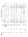
- FIG. 3 is a timing chart for explaining an operation of a touch location detector 30.
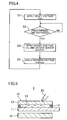
- FIG. 4 is a flowchart showing an operation of the phototransistor 31 in the present embodiment.
- FIG. 5 is a cross-sectional view schematically showing a structure of the liquid crystal display device 1 of the present embodiment.
- liquid crystal display device 1 will be described as an example display device.
- the liquid crystal display device 1 includes a liquid crystal display panel 10 and a backlight unit 15 located on the back side of the liquid crystal display panel 10 (i.e., on the side opposite to the side facing the user) as shown in FIG. 5 .
- the liquid crystal display panel 10 includes a TFT substrate 11 as a first substrate, and a counter substrate 12 as a second substrate opposed to the TFT substrate 11.
- a liquid crystal layer 13 surrounded and sealed by a frame-shaped sealing material 14 is provided between the TFT substrate 11 and the counter substrate 12.
- the liquid crystal layer is made of a nematic LC material, for example.
- the sealing material 14 is made of an epoxy resin which is cured, for example, by ultraviolet light or heat.
- the counter substrate 12 includes a color filter (not shown) having pigmented layers of R, G, B, a common electrode (not shown) made of a transparent conductive film such as an ITO film, a black matrix (not shown) serving as a light-shielding layer, etc.
- the liquid crystal display panel 10 includes a display region (not shown) and a frame-shaped non-display region surrounding the display region.
- a plurality of pixels 17 are provided in a matrix.
- Each of the pixels 17 includes three picture elements 18r, 18g, 18b as shown in FIG. 2 .
- the picture element 18r shows a red color (R); the picture element 18g shows a green color (G); and the picture element 18b shows a blue color (B).
- a picture element is a minimum unit for displaying each color, and is also called a dot.
- the TFT substrate 11 is a so-called active matrix substrate.
- a plurality of gate lines 21 which extend parallel to each other are provided on the TFT substrate 11, as shown in FIG. 2 .
- a plurality of source lines 22 which extend parallel to each other, and which intersect with the gate lines 21 at right angles, are also provided on the TFT substrate 11.
- a plurality of capacity lines 23 each of which is located between adjacent gate lines 21, and which extend parallel to each other are provided on the TFT substrate 11.
- Each of the picture elements 18r, 18g, 18b is provided, for example, in an area surrounded by adjacent source lines 22 and adjacent capacity lines 23.
- Each of the picture elements 18r, 18g, 18b includes a picture element electrode (not shown) for driving the liquid crystal layer 13, and a thin film transistor (TFT) 24 for driving the picture element electrode by switching.
- a source electrode (not shown) of the TFT 24 is connected to the source line 22.
- a gate electrode (not shown) of the TFT 24 is connected to the gate line 21.
- a drain electrode (not shown) of the TFT 24 is connected to the picture element electrode.
- Each of the picture elements 18r, 18g, 18b includes a liquid crystal capacitor 25 formed between the picture element electrode and the common electrode of the counter substrate 12, and an auxiliary capacitor 26 for maintaining the liquid crystal capacity constant.
- the auxiliary capacitor 26 is located between the drain electrode of the TFT 24 and the capacity line 23.
- the TFT 24 is turned on by a scan signal sent to the TFT 24 through the gate line 21, and in this state, an image signal is sent to the picture element electrode through the source line 22 via the TFT 24. As a result, a desired image is displayed.
- the liquid crystal display device 1 further includes a plurality of phototransistors 31, and is configured to detect, by the phototransistors 31, a touch location of an object 20, such as a finger of the user, on a display screen (a display region).
- a touch location detector 30 for detecting a touch location of the object 20 is provided in each of the pixels 17.
- the touch location detector 30 includes the phototransistor 31, a capacitor section 32, and an amplifier section 33 as shown in FIG. 2 .
- a first line 41 which extends along the capacity line 23, and a second line 42 and a third line 43 which extend along the gate line 21 are provided on the TFT substrate 11 such that the first line 41, the second line 42, and the third line 43 pass through each of the pixels 17.
- the amplifier section 33 is made, for example, of a TFT.
- a gate electrode 37 of the amplifier section 33 is connected to the output side of the capacitor section 32.
- a source electrode 38 of the amplifier section 33 is connected to one source line 22a (e.g., a source line 22a positioned at a boundary between the adjacent picture elements 18r and 18g as shown in FIG. 2 ).
- a drain electrode 39 of the amplifier section 33 is connected to a source line 22b which is positioned next to the source line 22a, and by which the picture element 18r is partitioned.
- a detecting section 35 for detecting an output signal of the amplifier section 33 is connected to the source line 22b.
- the input side of the capacitor section 32 is connected to the second line 42 and a drain electrode 50 of the phototransistor 31.
- an output value of the touch location detector 30 which corresponds to an amount of light received is detected by the detecting section 35 for each of the pixels 17.
- the liquid crystal display device 1 can detect a touch location on the display screen.
- a structure of the phototransistor 31 will be described in detail with reference to FIG. 1 and FIG. 2 .
- the phototransistor 31 is provided on a glass substrate 45 which is an insulating substrate forming the TFT substrate 11.
- the phototransistor 31 has a bottom-gate structure. That is, the phototransistor 31 includes: a gate electrode 46 formed on the glass substrate 45; a gate insulating film 47 which covers the gate electrode 46; a semiconductor layer 48 provided on a surface of the gate insulating film 47 and having a channel region 55 opposed to the gate electrode 46; a source electrode 49 and a drain electrode 50 which cover respective portions of the semiconductor layer 48; and an interlayer insulating film 51 which covers the channel region 55 of the semiconductor layer 48, the source electrode 49, and the drain electrode 50.
- the gate electrode 46 is made, for example, of a light-shielding layer of a metal such as an aluminum alloy or chromium alloy.
- the channel region 55 of the semiconductor layer 48 is made of amorphous silicon (a-Si). Impurity areas made of n+ silicon 54 are formed in the semiconductor layer 48 on both lateral sides of the channel region 55.
- a portion 56 of the channel region 55, the portion 56 facing a transparent electrode 52 is also referred to as a back channel 56.
- the back channel 56 is an area of the channel region 55 which is not in contact with the gate insulating film 47, and which is also not in contact with the source electrode 49 and the drain electrode 50.
- the interlayer insulating film 51 is, for example, a PAS film (i.e., a passivation film), a JAS film (i.e., an acrylic organic resin film), etc.
- each of the source electrode 49 and the drain electrode 50 is made, for example, of a light-shielding layer of a metal such as an aluminum alloy or chromium alloy.
- the source electrode 49 and the gate electrode 46 have the same electric potential. Both of the source electrode 49 and the gate electrode 46 are connected to the first line 41.
- the source electrode 49 and the gate electrode 46 may be connected to each other, or may be made to have the same electric potential by a voltage applied through another line.
- the phototransistor 31 further includes the transparent electrode 52 provided on the surface of the interlayer insulating film 51 so as to be located above the channel region 55, and includes a refresh controller 34.
- the transparent electrode 52 is made, for example, of a transparent conductive film, such as an ITO film, and therefore transmits excitation light (in this case, outside light which is visible light).
- This transparent electrode 52 is connected to the third line 43.
- the interlayer insulating film 51 is preferably thin to reduce the space between the transparent electrode 52 and the back channel 56, and increase electric field effect. It is possible to provide a transparent organic insulating film, etc. for covering the transparent electrode 52.
- the refresh controller 34 is connected to the first line 41, the second line 42 and the third line 43, as shown in FIG. 2 . As shown in FIG. 1 , the refresh controller 34 is configured to reduce a charge accumulated in the portion 56 of the channel region 55, the portion 56 facing the transparent electrode 52 (i.e., the back channel 56), by applying a voltage between the transparent electrode 52, and the gate electrode 46, the source electrode 49 and the drain electrode 50.
- a voltage may be applied between the transparent electrode 52, and the gate electrode 46 and the source electrode 49.
- the refresh controller 34 is configured to apply the above voltage at every predetermined time. For example, it is preferable to apply the voltage at every vertical period.
- 1 vertical period (1 frame period) is a period which is needed so that a voltage is applied to the liquid crystal layer 13 of all of the pixels 17 of the liquid crystal display device 1, and one screen image is displayed on the screen.
- FIG. 3A is a timing chart showing a scan signal input to the gate line 21.
- FIG. 3B is a timing chart showing a simplified image signal input to the source line 22.
- FIG. 3C is a timing chart showing a signal voltage input to the capacity line 23.
- FIG. 3D is a timing chart showing a boost voltage V rw input to the second line 42.
- FIG. 3E is a timing chart showing a reset voltage V rst input to the first line 41.
- FIG. 3F is a timing chart showing a source voltage V s input to the source line 22a connected to the amplifier section 33.
- FIG. 3G is a timing chart showing an estimated value of a voltage V NetA generated at a NetA section 36.
- FIG. 3H is a timing chart showing an output voltage V o output from the amplifier section 33.
- FIG. 3I is a timing chart showing a refresh voltage V refresh input to the third line 43.
- a series of touch location detecting operations is performed by the touch location detector 30 at every predetermined time.
- the series of touch location detecting operations is performed at every vertical period.
- step S1 the refresh controller 34 applies a reset voltage V rst , for example, of -4 V to the gate electrode 46 and the source electrode 49 of the phototransistor 31 through the first line 41, as shown in FIG. 3E .
- the reset voltage V rst is forward biased with respect to the phototransistor 31.
- the gate of the phototransistor 31 is turned on, and the reset voltage V rst is input to the capacitor section 32 via the drain electrode 50.
- FIG. 3G the voltage V NetA of the NetA section 36 which is on the output side of the capacitor section 32 is reset.
- step S2 it is determined whether predetermined time (1 vertical period) has passed or not. If the phototransistor 31 receives light during this 1 vertical period without being touched by an object 20, a reverse current flows to the phototransistor 31 in accordance with the amount of light received, and the voltage V NetA of the NetA section 36 drops as shown in FIG. 3G . On the other hand, if light is blocked by the touch of the object 20, no reverse current flows in the phototransistor 31, and therefore, the voltage V NetA of the NetA section 36 does not drop, and is maintained.
- step S3 the refresh controller 34 inputs a boost voltage V rw , for example, of +24 V to the capacitor section 32 through the second line 42.
- V rw boost voltage
- the voltage V NetA of the NetA section 36 is boosted and increased.
- the gate of the amplifier section 33 is turned on at this time.
- the output voltage V o corresponding to the magnitude of the boosted voltage V NetA of the NetA section 36 passes through the amplifier section 33, and is detected by the detecting section 35. The state of being touched or the state of being untouched at the pixel 17 which includes the phototransistor 31 is detected based on the detected output voltage V o .
- step S4 the refresh controller 34 applies a refresh voltage V refresh , for example, of -20 V to the transparent electrode 52 through the third line 43 as shown in FIG. 3I .
- a boost voltage V rw for example, of +24 V is applied at this time to the drain electrode 50 of the phototransistor 31 through the second line 42.
- a reset voltage V rst for example, of -4 V is applied to the gate electrode 46 and the source electrode 49 of the phototransistor 31 through the first line 41.
- the voltage value of the source line 22a is set to 0 V as shown in FIG. 3F .
- FIG. 6 is a graph showing a threshold characteristic of the phototransistor 31 which had received light and deteriorated with time.
- FIG. 7 is a graph showing a threshold characteristic of the phototransistor 31 after refresh control.
- the graph 60 of FIG. 6 indicates a characteristic of the initial state before receiving light.
- the graph 61 of FIG. 6 indicates a characteristic of the phototransistor which continuously received light in an environment of about 10 klx. As shown in FIG. 6 , if the phototransistor receives light continuously, the characteristic of the phototransistor deteriorates with time, and a threshold value V th shifts to the direction of positive values (i.e., to the right in FIG. 6 ).
- the amorphous silicon in the channel region received strong light, which increases the number of dangling bonds and a defect density, and as a result, carriers cannot move easily.
- the graph 61 of FIG. 7 indicates a characteristic of the phototransistor 31 of the present example after receiving light.
- the graph 62 of FIG. 7 indicates a characteristic immediately after refresh control.
- a threshold value V th shifts to the direction of negative values (i.e., to the left in FIG. 7 ). This means that the phototransistor 31 could be brought close to the initial state.
- the phototransistor 31 is provided with the transparent electrode 52 and the refresh controller 34.
- a voltage is applied between the transparent electrode 52, and the gate electrode 46 and the source electrode 49, by the refresh controller 34, thereby making it possible to form an electric field in the back channel 56.
- the charge accumulated in the back channel 56 due to continuous light receiving can be reduced by this electric field.
- carriers in the channel region 55 can move easily, and the light-receiving characteristics of the phototransistor 31 can be brought close to the initial state.
- generating the electric field (i.e., performing refresh control) by this refresh controller 34 at every predetermined time can maintain favorable light-receiving characteristics of the phototransistor 31, and high sensor accuracy.
- the refresh control by the refresh controller 34 is performed at every vertical period.
- the favorable light-receiving characteristics of the phototransistor 31 can be maintained for each one screen image display.
- the electrode provided above the back channel 56 is the transparent electrode 52 which transmits outside light (excitation light).
- the transparent electrode 52 which transmits outside light (excitation light).
- the charge accumulated in the back channel 56 can be more effectively reduced.
- the voltage value of the source line 22a is set to 0 V during the refresh control as shown in FIG. 3F , it is possible to prevent a significantly boosted voltage from being applied to the detecting section 35 or other driver circuits through the source line 22b. As a result, circuits such as the detecting section 35 can be protected.
- the liquid crystal display device 1 was described in the above embodiment. However, the present invention is not limited to the liquid crystal display device 1, and can also be applied to display devices such as an organic EL display device.
- the present invention is useful as a phototransistor and a display device having the phototransistor.
Landscapes
- Engineering & Computer Science (AREA)
- General Engineering & Computer Science (AREA)
- Theoretical Computer Science (AREA)
- Human Computer Interaction (AREA)
- Physics & Mathematics (AREA)
- General Physics & Mathematics (AREA)
- Liquid Crystal (AREA)
- Position Input By Displaying (AREA)
Abstract
Description
- The present invention relates to a phototransistor and a display device including the phototransistor.
- In recent years, attention has been given to touch panel devices as input means for devices. A resistive layer type, an optical type, etc., are generally known as types of the touch panel devices. For example, layering the touch panel devices on a liquid crystal display panel to provide a liquid crystal display device with a touch panel had been known. However, the problem in this technique was that the thickness of the display device was increased. To reduce the thickness of the device as a whole, providing a plurality of optical sensors to the liquid crystal display panel so that the liquid crystal display panel itself has a function of a touch panel has been known. The optical sensors are, for example, phototransistors.
- In the liquid crystal display panel which has a function of a touch panel, a current flows in the optical sensors in the area where light is not blocked, whereas no current flows in the optical sensors in the area where light is blocked by the contact of an object such as a finger of the user. This is how the contact location (i.e., a touch location) is detected.
- However, characteristics of the optical sensors, such as phototransistors, may deteriorate with time and use, which may result in a reduction in sensitivity of the sensors.
-
Patent Document 1 discloses a liquid crystal display device which includes a backlight and a light source for adjusting brightness. Brightness of light emitted from the backlight, and brightness of light emitted from the light source for adjusting brightness, are separately detected to obtain ratios between the brightness of light of the light sources. Based on comparison between the brightness ratios, a current value of drive current to be supplied to the backlight is adjusted (corrected), thereby controlling the brightness of light. Therefore, even if light-emitting characteristics of the backlight, or light-receiving characteristics of the optical sensors are deteriorated, brightness of the display light is properly maintained. Patent Document 2 discloses an image reader having a so-called double gate phototransistor, wherein a pulse voltage is applied to a top gate electrode in a reset operation, and a high level bias voltage is applied to a bottom gate electrode in a readout operation. -
- Patent Document 1: Japanese Patent Publication No.
2007-250252 - Patent Document 2: Japanese Patent Publication No.
2002-259955 - However, in
Patent Documents 1 and 2, no measure is taken to reduce age deterioration of light-receiving characteristics of the optical sensors. - Thus, the liquid crystal display device disclosed in
Patent Document 1 has a problem that another light source for adjusting brightness is needed to properly maintain the brightness of the display light. Further, a reduction in sensor detection accuracy is inevitable in the phototransistor disclosed in Patent Document 2. - The present invention was made in view of the above problems, and it is an objective of the invention to make it possible to favorably maintain the light-receiving characteristics of a phototransistor.
- To achieve the above objective, a transparent electrode and a refresh controller are provided in the present invention to reduce a charge accumulated in a portion of a channel region, the portion facing the transparent electrode.
- Specifically, the first aspect of the present invention is intended for a phototransistor including: a gate electrode formed on an insulating substrate; a gate insulating film which covers the gate electrode; a semiconductor layer which is formed on a surface of the gate insulating film, and has a channel region opposed to the gate electrode; a source electrode and a drain electrode which cover respective portions of the semiconductor layer; and an interlayer insulating film which covers the channel region of the semiconductor layer, the source electrode and the drain electrode. The source electrode and the gate electrode have the same electric potential, and the phototransistor includes a transparent electrode formed on a surface of the interlayer insulating film so as to overlap the channel region, and a refresh controller for reducing a charge accumulated in a portion of the channel region, the portion facing the transparent electrode, by applying a voltage between the transparent electrode, and the gate electrode and the source electrode.
- According to the first aspect of the present invention, when the light having been transmitted through the transparent electrode enters the channel region of the semiconductor layer, the semiconductor layer is reverse biased, and a current starts to flow. By detecting this current, it is possible to detect the amount of light received under predetermined light-receiving characteristics. However, the light-receiving characteristics deteriorate with time and use. This may be because a charge is accumulated in a portion of the channel region, the portion facing the transparent electrode. Thus, in the present invention, the charge accumulated in the portion of the channel region, the portion facing the transparent electrode, is reduced by applying a voltage between the transparent electrode, and the gate electrode and the source electrode, by the refresh controller. As a result, the light-receiving characteristics of the phototransistor can be favorably maintained.
- The second aspect of the present invention is that the refresh controller applies the voltage between the transparent electrode, and the gate electrode, the source electrode and the drain electrode to reduce the charge, in the first aspect of the present invention.
- According to the second aspect of the present invention, a voltage is applied by the refresh controller not only between the transparent electrode, and the gate electrode and the source electrode, but also between the transparent electrode and the drain electrode. Thus, the charge accumulated in the portion of the channel region, the portion facing the transparent electrode, can be more effectively reduced.
- The third aspect of the present invention is that in the phototransistor of the first or second aspect of the present invention, the refresh controller applies the voltage at every predetermined time.
- According to the third aspect of the present invention, the voltage is applied by the refresh controller at every predetermined time. Thus, the light-receiving characteristics of the phototransistor can be more favorably maintained.
- The fourth aspect of the present invention is intended for a display device including a plurality of phototransistors by which a location touched by an object on a display screen is detected. Each of the phototransistors includes: a gate electrode formed on an insulating substrate; a gate insulating film which covers the gate electrode; a semiconductor layer which is formed on a surface of the gate insulating film, and has a channel region opposed to the gate electrode; a source electrode and a drain electrode which cover respective portions of the semiconductor layer; and an interlayer insulating film which covers the channel region of the semiconductor layer, the source electrode and the drain electrode. The source electrode and the gate electrode have the same electric potential, and each of the phototransistors includes a transparent electrode formed on a surface of the interlayer insulating film so as to cover the channel region, and a refresh controller for reducing a charge accumulated in a portion of the channel region, the portion facing the transparent electrode, by applying a voltage between the transparent electrode, and the gate electrode and the source electrode.
- According to the fourth aspect of the present invention, when an object comes into contact with the display screen, outside light is blocked by the object at the touch location (i.e., a contact location), and a current flows through the phototransistor located at the touch location. By detecting this current, it is possible to detect the amount of light received under predetermined light-receiving characteristics. The light-receiving characteristics of the phototransistor deteriorate with time as described above. However, in the present invention, a voltage is applied by the refresh controller between the transparent electrode, and the gate electrode and the source electrode to reduce the charge accumulated in the portion of the channel region, the portion facing the transparent electrode. As a result, the light-receiving characteristics of the phototransistor can be favorably maintained.
- The fifth aspect of the present invention is that the refresh controller applies the voltage between the transparent electrode, and the gate electrode, the source electrode and the drain electrode to reduce the charge, in the fourth aspect of the present invention.
- According to the fifth aspect of the present invention, a voltage is applied by the refresh controller not only between the transparent electrode, and the gate electrode and the source electrode, but also between the transparent electrode and the drain electrode. Thus, the charge accumulated in the portion of the channel region, the portion facing the transparent electrode, can be more effectively reduced.
- The sixth aspect of the present invention is that the refresh controller applies the voltage at every predetermined time in the fourth or fifth aspect of the present invention.
- According to the sixth aspect of the present invention, the voltage is applied by the refresh controller at every predetermined time. Thus, the light-receiving characteristics of the phototransistor can be more favorably maintained.
- The seventh aspect of the present invention is that the refresh controller applies the voltage at every vertical period in the sixth aspect of the present invention.
- According to the seventh aspect of the present invention, the voltage is applied by the refresh controller at every vertical period. Thus, favorable light-receiving characteristics of the phototransistor can be maintained for each display image.
- According to the present invention, a voltage is applied between a transparent electrode, and a gate electrode and a source electrode by a refresh controller, thereby reducing a charge accumulated in a portion of a channel region, the portion facing a transparent electrode. Thus, light-receiving characteristics of the phototransistor can be favorably maintained.
-
-
FIG. 1 is an enlarged cross-sectional view of a structure of a phototransistor in the present embodiment. -
FIG. 2 is a circuit diagram showing pixels of a liquid crystal display device in the present embodiment. -
FIG. 3A is a timing chart showing a scan signal input to a gate line.FIG. 3B is a timing chart showing a simplified image signal input to a source line.FIG. 3C is a timing chart showing a signal voltage input to a capacity line.FIG. 3D is a timing chart showing a boost voltage Vrw input to a second line.FIG. 3E is a timing chart showing a reset voltage Vrst input to a first line.FIG. 3F is a timing chart showing a source voltage Vs input to a source line connected to an amplifier section.FIG. 3G is a timing chart showing an estimated value of a voltage VNetA generated at an NetA section.FIG. 3H is a timing chart showing an output voltage Vo output from the amplifier section.FIG. 3I is a timing chart showing a refresh voltage Vrefresh input to a third line. -
FIG. 4 is a flowchart showing an operation of the phototransistor in the present embodiment. -
FIG. 5 is a cross-sectional view schematically showing a structure of the liquid crystal display device of the present embodiment. -
FIG. 6 is a graph showing a threshold characteristic of a phototransistor which had received light and deteriorated with time. -
FIG. 7 is a graph showing a threshold characteristic of a phototransistor after refresh control. - An embodiment of the present invention will be described in detail below based on the drawings. The present invention is not limited to the embodiment below.
-
FIGS. 1-7 show an embodiment of the present invention. -
FIG. 1 is an enlarged cross-sectional view of a structure of aphototransistor 31 in the present embodiment.FIG. 2 is a circuitdiagram showing pixels 17 of a liquidcrystal display device 1 in the present embodiment.FIG. 3 is a timing chart for explaining an operation of atouch location detector 30.FIG. 4 is a flowchart showing an operation of thephototransistor 31 in the present embodiment.FIG. 5 is a cross-sectional view schematically showing a structure of the liquidcrystal display device 1 of the present embodiment. - In the present embodiment, the liquid
crystal display device 1 will be described as an example display device. - The liquid
crystal display device 1 includes a liquidcrystal display panel 10 and abacklight unit 15 located on the back side of the liquid crystal display panel 10 (i.e., on the side opposite to the side facing the user) as shown inFIG. 5 . - The liquid
crystal display panel 10 includes aTFT substrate 11 as a first substrate, and acounter substrate 12 as a second substrate opposed to theTFT substrate 11. Aliquid crystal layer 13 surrounded and sealed by a frame-shapedsealing material 14 is provided between theTFT substrate 11 and thecounter substrate 12. The liquid crystal layer is made of a nematic LC material, for example. The sealingmaterial 14 is made of an epoxy resin which is cured, for example, by ultraviolet light or heat. - The
counter substrate 12 includes a color filter (not shown) having pigmented layers of R, G, B, a common electrode (not shown) made of a transparent conductive film such as an ITO film, a black matrix (not shown) serving as a light-shielding layer, etc. - The liquid
crystal display panel 10 includes a display region (not shown) and a frame-shaped non-display region surrounding the display region. In the display region, a plurality ofpixels 17 are provided in a matrix. Each of thepixels 17 includes threepicture elements FIG. 2 . Thepicture element 18r shows a red color (R); thepicture element 18g shows a green color (G); and thepicture element 18b shows a blue color (B). Here, a picture element is a minimum unit for displaying each color, and is also called a dot. - The
TFT substrate 11 is a so-called active matrix substrate. A plurality ofgate lines 21 which extend parallel to each other are provided on theTFT substrate 11, as shown inFIG. 2 . Further, a plurality ofsource lines 22 which extend parallel to each other, and which intersect with the gate lines 21 at right angles, are also provided on theTFT substrate 11. Moreover, a plurality ofcapacity lines 23 each of which is located betweenadjacent gate lines 21, and which extend parallel to each other are provided on theTFT substrate 11. - Each of the
picture elements adjacent source lines 22 and adjacent capacity lines 23. Each of thepicture elements liquid crystal layer 13, and a thin film transistor (TFT) 24 for driving the picture element electrode by switching. A source electrode (not shown) of the TFT 24 is connected to thesource line 22. A gate electrode (not shown) of the TFT 24 is connected to thegate line 21. A drain electrode (not shown) of the TFT 24 is connected to the picture element electrode. - Each of the
picture elements liquid crystal capacitor 25 formed between the picture element electrode and the common electrode of thecounter substrate 12, and anauxiliary capacitor 26 for maintaining the liquid crystal capacity constant. Theauxiliary capacitor 26 is located between the drain electrode of the TFT 24 and thecapacity line 23. - In the liquid
crystal display device 1, the TFT 24 is turned on by a scan signal sent to the TFT 24 through thegate line 21, and in this state, an image signal is sent to the picture element electrode through thesource line 22 via the TFT 24. As a result, a desired image is displayed. - The liquid
crystal display device 1 further includes a plurality ofphototransistors 31, and is configured to detect, by thephototransistors 31, a touch location of anobject 20, such as a finger of the user, on a display screen (a display region). - Specifically, in the liquid
crystal display device 1, atouch location detector 30 for detecting a touch location of theobject 20 is provided in each of thepixels 17. Thetouch location detector 30 includes thephototransistor 31, acapacitor section 32, and anamplifier section 33 as shown inFIG. 2 . - A
first line 41 which extends along thecapacity line 23, and asecond line 42 and athird line 43 which extend along thegate line 21 are provided on theTFT substrate 11 such that thefirst line 41, thesecond line 42, and thethird line 43 pass through each of thepixels 17. - The
amplifier section 33 is made, for example, of a TFT. Agate electrode 37 of theamplifier section 33 is connected to the output side of thecapacitor section 32. Asource electrode 38 of theamplifier section 33 is connected to onesource line 22a (e.g., asource line 22a positioned at a boundary between theadjacent picture elements FIG. 2 ). Adrain electrode 39 of theamplifier section 33 is connected to asource line 22b which is positioned next to thesource line 22a, and by which thepicture element 18r is partitioned. A detectingsection 35 for detecting an output signal of theamplifier section 33 is connected to thesource line 22b. - The input side of the
capacitor section 32 is connected to thesecond line 42 and adrain electrode 50 of thephototransistor 31. - Thus, an output value of the
touch location detector 30 which corresponds to an amount of light received is detected by the detectingsection 35 for each of thepixels 17. With this structure, the liquidcrystal display device 1 can detect a touch location on the display screen. - A structure of the
phototransistor 31 will be described in detail with reference toFIG. 1 andFIG. 2 . - The
phototransistor 31 is provided on aglass substrate 45 which is an insulating substrate forming theTFT substrate 11. Thephototransistor 31 has a bottom-gate structure. That is, thephototransistor 31 includes: agate electrode 46 formed on theglass substrate 45; agate insulating film 47 which covers thegate electrode 46; asemiconductor layer 48 provided on a surface of thegate insulating film 47 and having achannel region 55 opposed to thegate electrode 46; asource electrode 49 and adrain electrode 50 which cover respective portions of thesemiconductor layer 48; and aninterlayer insulating film 51 which covers thechannel region 55 of thesemiconductor layer 48, thesource electrode 49, and thedrain electrode 50. - The
gate electrode 46 is made, for example, of a light-shielding layer of a metal such as an aluminum alloy or chromium alloy. Thechannel region 55 of thesemiconductor layer 48 is made of amorphous silicon (a-Si). Impurity areas made ofn+ silicon 54 are formed in thesemiconductor layer 48 on both lateral sides of thechannel region 55. - A
portion 56 of thechannel region 55, theportion 56 facing a transparent electrode 52 (i.e., the portion of thechannel region 55 indicated by dot-dot-dash line inFIG. 1 ), is also referred to as aback channel 56. Theback channel 56 is an area of thechannel region 55 which is not in contact with thegate insulating film 47, and which is also not in contact with thesource electrode 49 and thedrain electrode 50. - The
interlayer insulating film 51 is, for example, a PAS film (i.e., a passivation film), a JAS film (i.e., an acrylic organic resin film), etc. Further, each of thesource electrode 49 and thedrain electrode 50 is made, for example, of a light-shielding layer of a metal such as an aluminum alloy or chromium alloy. Thesource electrode 49 and thegate electrode 46 have the same electric potential. Both of thesource electrode 49 and thegate electrode 46 are connected to thefirst line 41. Thesource electrode 49 and thegate electrode 46 may be connected to each other, or may be made to have the same electric potential by a voltage applied through another line. - The
phototransistor 31 further includes thetransparent electrode 52 provided on the surface of theinterlayer insulating film 51 so as to be located above thechannel region 55, and includes arefresh controller 34. - The
transparent electrode 52 is made, for example, of a transparent conductive film, such as an ITO film, and therefore transmits excitation light (in this case, outside light which is visible light). Thistransparent electrode 52 is connected to thethird line 43. Theinterlayer insulating film 51 is preferably thin to reduce the space between thetransparent electrode 52 and theback channel 56, and increase electric field effect. It is possible to provide a transparent organic insulating film, etc. for covering thetransparent electrode 52. - The
refresh controller 34 is connected to thefirst line 41, thesecond line 42 and thethird line 43, as shown inFIG. 2 . As shown inFIG. 1 , therefresh controller 34 is configured to reduce a charge accumulated in theportion 56 of thechannel region 55, theportion 56 facing the transparent electrode 52 (i.e., the back channel 56), by applying a voltage between thetransparent electrode 52, and thegate electrode 46, thesource electrode 49 and thedrain electrode 50. - To reduce the charge accumulated in the
back channel 56, a voltage may be applied between thetransparent electrode 52, and thegate electrode 46 and thesource electrode 49. However, to effectively reduce the above charge, it is preferable to apply a voltage not only to thegate electrode 46 and thesource electrode 49, but also to thedrain electrode 50 as described above. - Further, the
refresh controller 34 is configured to apply the above voltage at every predetermined time. For example, it is preferable to apply the voltage at every vertical period. - Here, 1 vertical period (1 frame period) is a period which is needed so that a voltage is applied to the
liquid crystal layer 13 of all of thepixels 17 of the liquidcrystal display device 1, and one screen image is displayed on the screen. - Now, operation of the
touch location detector 30 of the liquidcrystal display device 1 will be described with reference toFIG. 3 andFIG. 4 . -
FIG. 3A is a timing chart showing a scan signal input to thegate line 21.FIG. 3B is a timing chart showing a simplified image signal input to thesource line 22.FIG. 3C is a timing chart showing a signal voltage input to thecapacity line 23.FIG. 3D is a timing chart showing a boost voltage Vrw input to thesecond line 42.FIG. 3E is a timing chart showing a reset voltage Vrst input to thefirst line 41. -
FIG. 3F is a timing chart showing a source voltage Vs input to thesource line 22a connected to theamplifier section 33.FIG. 3G is a timing chart showing an estimated value of a voltage VNetA generated at aNetA section 36.FIG. 3H is a timing chart showing an output voltage Vo output from theamplifier section 33.FIG. 3I is a timing chart showing a refresh voltage Vrefresh input to thethird line 43. - A series of touch location detecting operations is performed by the
touch location detector 30 at every predetermined time. In the present embodiment, a case in which the series of touch location detecting operations is performed at every vertical period will be described. - First, in step S1, the
refresh controller 34 applies a reset voltage Vrst, for example, of -4 V to thegate electrode 46 and thesource electrode 49 of thephototransistor 31 through thefirst line 41, as shown inFIG. 3E . The reset voltage Vrst is forward biased with respect to thephototransistor 31. Thus, the gate of thephototransistor 31 is turned on, and the reset voltage Vrst is input to thecapacitor section 32 via thedrain electrode 50. As a result, as shown inFIG. 3G , the voltage VNetA of theNetA section 36 which is on the output side of thecapacitor section 32 is reset. - Next, in step S2, it is determined whether predetermined time (1 vertical period) has passed or not. If the
phototransistor 31 receives light during this 1 vertical period without being touched by anobject 20, a reverse current flows to thephototransistor 31 in accordance with the amount of light received, and the voltage VNetA of theNetA section 36 drops as shown inFIG. 3G . On the other hand, if light is blocked by the touch of theobject 20, no reverse current flows in thephototransistor 31, and therefore, the voltage VNetA of theNetA section 36 does not drop, and is maintained. - After 1 vertical period has passed, the operation goes to step S3. In step S3, the
refresh controller 34 inputs a boost voltage Vrw, for example, of +24 V to thecapacitor section 32 through thesecond line 42. Thus, as shown inFIG. 3D and FIG. 3G , the voltage VNetA of theNetA section 36 is boosted and increased. Further, the gate of theamplifier section 33 is turned on at this time. As shown inFIG. 3H , the output voltage Vo corresponding to the magnitude of the boosted voltage VNetA of theNetA section 36 passes through theamplifier section 33, and is detected by the detectingsection 35. The state of being touched or the state of being untouched at thepixel 17 which includes thephototransistor 31 is detected based on the detected output voltage Vo. - Next, in step S4, the
refresh controller 34 applies a refresh voltage Vrefresh, for example, of -20 V to thetransparent electrode 52 through thethird line 43 as shown inFIG. 3I . As shown inFIG. 3D , a boost voltage Vrw, for example, of +24 V is applied at this time to thedrain electrode 50 of thephototransistor 31 through thesecond line 42. Further, as shown inFIG. 3E , a reset voltage Vrst, for example, of -4 V is applied to thegate electrode 46 and thesource electrode 49 of thephototransistor 31 through thefirst line 41. Moreover, at this time, the voltage value of thesource line 22a is set to 0 V as shown inFIG. 3F . - As a result, an electric field is generated between the
transparent electrode 52 having a negative electric potential and thegate electrode 46, thesource electrode 49 and thedrain electrode 50 each having a positive electric potential. Thus, holes gather at theback channel 56, which means that a charge (electrons) accumulated at theback channel 56 is reduced. -
FIG. 6 is a graph showing a threshold characteristic of thephototransistor 31 which had received light and deteriorated with time.FIG. 7 is a graph showing a threshold characteristic of thephototransistor 31 after refresh control. - The
graph 60 ofFIG. 6 indicates a characteristic of the initial state before receiving light. On the other hand, thegraph 61 ofFIG. 6 indicates a characteristic of the phototransistor which continuously received light in an environment of about 10 klx. As shown inFIG. 6 , if the phototransistor receives light continuously, the characteristic of the phototransistor deteriorates with time, and a threshold value Vth shifts to the direction of positive values (i.e., to the right inFIG. 6 ). - This may be because the amorphous silicon in the channel region received strong light, which increases the number of dangling bonds and a defect density, and as a result, carriers cannot move easily.
- The
graph 61 ofFIG. 7 indicates a characteristic of thephototransistor 31 of the present example after receiving light. Thegraph 62 ofFIG. 7 indicates a characteristic immediately after refresh control. As shown inFIG. 7 , a threshold value Vth shifts to the direction of negative values (i.e., to the left inFIG. 7 ). This means that thephototransistor 31 could be brought close to the initial state. - According to this first embodiment, the
phototransistor 31 is provided with thetransparent electrode 52 and therefresh controller 34. A voltage is applied between thetransparent electrode 52, and thegate electrode 46 and thesource electrode 49, by therefresh controller 34, thereby making it possible to form an electric field in theback channel 56. The charge accumulated in theback channel 56 due to continuous light receiving can be reduced by this electric field. As a result, carriers in thechannel region 55 can move easily, and the light-receiving characteristics of thephototransistor 31 can be brought close to the initial state. Thus, generating the electric field (i.e., performing refresh control) by thisrefresh controller 34 at every predetermined time can maintain favorable light-receiving characteristics of thephototransistor 31, and high sensor accuracy. - Further, the refresh control by the
refresh controller 34 is performed at every vertical period. Thus, the favorable light-receiving characteristics of thephototransistor 31 can be maintained for each one screen image display. - Further, the electrode provided above the
back channel 56 is thetransparent electrode 52 which transmits outside light (excitation light). Thus, it is possible to generate an electric field in theback channel 56 without impairing the function of thephototransistor 31 as an optical sensor. - Further, since a voltage is applied not only between the
transparent electrode 52, and thegate electrode 46 and thesource electrode 49, but also between thetransparent electrode 52 and thedrain electrode 50, the charge accumulated in theback channel 56 can be more effectively reduced. - Further, since the voltage value of the
source line 22a is set to 0 V during the refresh control as shown inFIG. 3F , it is possible to prevent a significantly boosted voltage from being applied to the detectingsection 35 or other driver circuits through thesource line 22b. As a result, circuits such as the detectingsection 35 can be protected. - The liquid
crystal display device 1 was described in the above embodiment. However, the present invention is not limited to the liquidcrystal display device 1, and can also be applied to display devices such as an organic EL display device. - As described above, the present invention is useful as a phototransistor and a display device having the phototransistor.
-
- 1
- liquid crystal display device
- 20
- object
- 30
- touch location detector
- 31
- phototransistor
- 32
- capacitor section
- 33
- amplifier section
- 34
- refresh controller
- 35
- detecting section
- 36
- NetA section
- 41
- first line
- 42
- second line
- 43
- third line
- 45
- glass substrate (insulating substrate)
- 46
- gate electrode
- 47
- gate insulating film
- 48
- semiconductor layer
- 49
- source electrode
- 50
- drain electrode
- 51
- interlayer insulating film
- 52
- transparent electrode
- 55
- channel region
- 56
- back channel (a portion of channel region, the portion facing a transparent electrode)
Claims (7)
- A phototransistor, comprising:a gate electrode formed on an insulating substrate;a gate insulating film which covers the gate electrode;a semiconductor layer which is formed on a surface of the gate insulating film, and has a channel region opposed to the gate electrode;a source electrode and a drain electrode which cover respective portions of the semiconductor layer; andan interlayer insulating film which covers the channel region of the semiconductor layer, the source electrode and the drain electrode, whereinthe source electrode and the gate electrode have the same electric potential, andthe phototransistor includes
a transparent electrode formed on a surface of the interlayer insulating film so as to overlap the channel region, and
a refresh controller for reducing a charge accumulated in a portion of the channel region, the portion facing the transparent electrode, by applying a voltage between the transparent electrode, and the gate electrode and the source electrode. - The phototransistor of claim 1, wherein
the refresh controller applies the voltage between the transparent electrode, and the gate electrode, the source electrode and the drain electrode to reduce the charge. - The phototransistor of claim 1 or 2, wherein
the refresh controller applies the voltage at every predetermined time. - A display device, comprising:a plurality of phototransistors by which a location touched by an object on a display screen is detected, whereineach of the phototransistors includes
a gate electrode formed on an insulating substrate,
a gate insulating film which covers the gate electrode,
a semiconductor layer which is formed on a surface of the gate insulating film, and has a channel region opposed to the gate electrode,
a source electrode and a drain electrode which cover respective portions of the semiconductor layer, and
an interlayer insulating film which covers the channel region of the semiconductor layer, the source electrode and the drain electrode,the source electrode and the gate electrode have the same electric potential, andeach of the phototransistors includes
a transparent electrode formed on a surface of the interlayer insulating film so as to overlap the channel region, and
a refresh controller for reducing a charge accumulated in a portion of the channel region, the portion facing the transparent electrode, by applying a voltage between the transparent electrode, and the gate electrode and the source electrode. - The display device of claim 4, wherein
the refresh controller applies the voltage between the transparent electrode, and the gate electrode, the source electrode and the drain electrode to reduce the charge. - The display device of claim 4 or 5, wherein
the refresh controller applies the voltage at every predetermined time. - The display device of claim 6, wherein
the refresh controller applies the voltage at every vertical period.
Applications Claiming Priority (2)
| Application Number | Priority Date | Filing Date | Title |
|---|---|---|---|
| JP2009152797 | 2009-06-26 | ||
| PCT/JP2010/000578 WO2010150431A1 (en) | 2009-06-26 | 2010-02-01 | Phototransistor, and a displaying device equipped therewith |
Publications (3)
| Publication Number | Publication Date |
|---|---|
| EP2448012A1 true EP2448012A1 (en) | 2012-05-02 |
| EP2448012A4 EP2448012A4 (en) | 2012-11-21 |
| EP2448012B1 EP2448012B1 (en) | 2013-12-18 |
Family
ID=43386222
Family Applications (1)
| Application Number | Title | Priority Date | Filing Date |
|---|---|---|---|
| EP10791759.3A Not-in-force EP2448012B1 (en) | 2009-06-26 | 2010-02-01 | Method of operating a PHOTOTRANSISTOR, AND A DISPLAYING DEVICE EQUIPPED THEREWITH |
Country Status (7)
| Country | Link |
|---|---|
| US (1) | US20120074474A1 (en) |
| EP (1) | EP2448012B1 (en) |
| JP (1) | JP5149993B2 (en) |
| CN (1) | CN102460734B (en) |
| BR (1) | BRPI1012257A2 (en) |
| RU (1) | RU2488193C1 (en) |
| WO (1) | WO2010150431A1 (en) |
Families Citing this family (9)
| Publication number | Priority date | Publication date | Assignee | Title |
|---|---|---|---|---|
| TWI475198B (en) * | 2013-05-15 | 2015-03-01 | Au Optronics Corp | Light sensing circuit |
| CN103336384B (en) * | 2013-06-28 | 2015-11-25 | 京东方科技集团股份有限公司 | A kind of display panel |
| US8803844B1 (en) * | 2013-10-02 | 2014-08-12 | DigiPuppets LLC | Capacitive finger puppet for use on touchscreen devices |
| US9985061B2 (en) * | 2014-03-20 | 2018-05-29 | Sharp Kabushiki Kaisha | Light detection device with integrated photodiode and thin film transistor |
| KR102293595B1 (en) | 2015-03-24 | 2021-08-25 | 삼성디스플레이 주식회사 | Thin film trannsistor array panel and manufacturing method thereof |
| JP6814429B2 (en) * | 2015-08-10 | 2021-01-20 | 天馬微電子有限公司 | Optical sensor element and photoelectric conversion device |
| US10439069B2 (en) * | 2015-08-10 | 2019-10-08 | Nlt Technologies, Ltd. | Optical sensor element and photoelectric conversion device |
| KR102554262B1 (en) * | 2018-12-28 | 2023-07-11 | 엘지디스플레이 주식회사 | Driving circuit, display panel and display device |
| CN111244196B (en) * | 2020-01-16 | 2021-09-14 | 云谷(固安)科技有限公司 | Light-sensitive thin film transistor, display panel and display device |
Family Cites Families (13)
| Publication number | Priority date | Publication date | Assignee | Title |
|---|---|---|---|---|
| RU1823931C (en) * | 1990-07-31 | 1993-06-23 | В.Н. Сведе-Швец, А.А. Авдеенко, А.В. Калинин, П.П. Нефидов, Е.И. Пак и И.В. Пол ков | Phototransistor |
| JP3019632B2 (en) * | 1992-10-16 | 2000-03-13 | カシオ計算機株式会社 | Photo sensor system and driving method thereof |
| JPH11345689A (en) * | 1998-06-01 | 1999-12-14 | Casio Comput Co Ltd | Display device |
| JP2001086293A (en) * | 1999-09-10 | 2001-03-30 | Casio Comput Co Ltd | Reader |
| JP2002259955A (en) * | 2001-03-05 | 2002-09-13 | Casio Comput Co Ltd | Image reading device |
| JP2006013407A (en) * | 2004-05-21 | 2006-01-12 | Sanyo Electric Co Ltd | Light amount detection circuit and display panel using the same |
| JP2006030317A (en) * | 2004-07-12 | 2006-02-02 | Sanyo Electric Co Ltd | Organic el display device |
| JP2006079589A (en) * | 2004-08-05 | 2006-03-23 | Sanyo Electric Co Ltd | Touch panel |
| KR101256663B1 (en) * | 2005-12-28 | 2013-04-19 | 엘지디스플레이 주식회사 | Liquid Crystal Display Device And fabricating Method and Driving Method Thereof |
| JP4898251B2 (en) * | 2006-03-14 | 2012-03-14 | パナソニック株式会社 | Method for forming conductive pattern, composition for forming conductive pattern, and electronic component having conductive pattern |
| JP4877480B2 (en) | 2006-03-14 | 2012-02-15 | カシオ計算機株式会社 | LIGHT SOURCE DEVICE, ITS CONTROL METHOD, AND DISPLAY DEVICE PROVIDED WITH THE LIGHT SOURCE DEVICE |
| KR100978263B1 (en) * | 2006-05-12 | 2010-08-26 | 엘지디스플레이 주식회사 | LCD and its manufacturing method |
| JP2008153427A (en) * | 2006-12-18 | 2008-07-03 | Hitachi Displays Ltd | High-sensitivity photosensor element and photosensor device using the same |
-
2010
- 2010-02-01 US US13/377,172 patent/US20120074474A1/en not_active Abandoned
- 2010-02-01 BR BRPI1012257A patent/BRPI1012257A2/en not_active IP Right Cessation
- 2010-02-01 CN CN201080026859.XA patent/CN102460734B/en not_active Expired - Fee Related
- 2010-02-01 RU RU2012102613/28A patent/RU2488193C1/en not_active IP Right Cessation
- 2010-02-01 JP JP2011519474A patent/JP5149993B2/en not_active Expired - Fee Related
- 2010-02-01 WO PCT/JP2010/000578 patent/WO2010150431A1/en not_active Ceased
- 2010-02-01 EP EP10791759.3A patent/EP2448012B1/en not_active Not-in-force
Also Published As
| Publication number | Publication date |
|---|---|
| US20120074474A1 (en) | 2012-03-29 |
| EP2448012A4 (en) | 2012-11-21 |
| CN102460734B (en) | 2014-08-27 |
| BRPI1012257A2 (en) | 2016-04-05 |
| JP5149993B2 (en) | 2013-02-20 |
| JPWO2010150431A1 (en) | 2012-12-06 |
| RU2488193C1 (en) | 2013-07-20 |
| CN102460734A (en) | 2012-05-16 |
| EP2448012B1 (en) | 2013-12-18 |
| WO2010150431A1 (en) | 2010-12-29 |
Similar Documents
| Publication | Publication Date | Title |
|---|---|---|
| EP2448012B1 (en) | Method of operating a PHOTOTRANSISTOR, AND A DISPLAYING DEVICE EQUIPPED THEREWITH | |
| US9362322B2 (en) | Light-sensing apparatus, method of driving the light-sensing apparatus, and optical touch screen apparatus including the light-sensing apparatus | |
| JP4925929B2 (en) | Display device | |
| US8368677B2 (en) | Optical sensor device, display apparatus, and method for driving optical sensor device | |
| TWI416484B (en) | Optical detection device, electro-optical device, electronic apparatus, and optical degradation correction method | |
| US7812906B2 (en) | Liquid crystal device and electronic apparatus | |
| JP5137680B2 (en) | Liquid crystal display | |
| JP5293197B2 (en) | Photoelectric conversion device, electro-optical device, electronic equipment | |
| JP5154378B2 (en) | Display device | |
| US20120327032A1 (en) | Light-sensing apparatuses, methods of driving the light-sensing apparatuses, and optical touch screen apparatuses including the light-sensing apparatuses | |
| JP2009288956A (en) | Organic el display device with touch panel function | |
| JP2008170837A (en) | Liquid crystal display | |
| JP2002023658A (en) | Dimming system | |
| JP5106784B2 (en) | Electro-optical device and electronic apparatus | |
| US9104259B2 (en) | Liquid crystal display device with touch panel | |
| US8810762B2 (en) | Display device equipped with touch sensor | |
| JP5163680B2 (en) | Display device | |
| JP5700073B2 (en) | Photoelectric conversion device, electro-optical device, electronic equipment | |
| JP5234090B2 (en) | Optical sensor device and driving method of optical sensor device | |
| KR101392573B1 (en) | Source driver of liquid crystal display and method for source driving | |
| JP5239293B2 (en) | Liquid crystal device and electronic device | |
| TWI479389B (en) | Optical sensor device, display apparatus, and method for driving optical sensor device | |
| US20120091319A1 (en) | Driving method for photosensor array panel | |
| JP2011054792A (en) | Optical sensor device and display device having the same | |
| JP2008294137A (en) | Optical sensor and display device |
Legal Events
| Date | Code | Title | Description |
|---|---|---|---|
| PUAI | Public reference made under article 153(3) epc to a published international application that has entered the european phase |
Free format text: ORIGINAL CODE: 0009012 |
|
| 17P | Request for examination filed |
Effective date: 20111220 |
|
| AK | Designated contracting states |
Kind code of ref document: A1 Designated state(s): AT BE BG CH CY CZ DE DK EE ES FI FR GB GR HR HU IE IS IT LI LT LU LV MC MK MT NL NO PL PT RO SE SI SK SM TR |
|
| DAX | Request for extension of the european patent (deleted) | ||
| A4 | Supplementary search report drawn up and despatched |
Effective date: 20121018 |
|
| RIC1 | Information provided on ipc code assigned before grant |
Ipc: G02F 1/1333 20060101ALI20121012BHEP Ipc: H01L 27/146 20060101ALI20121012BHEP Ipc: G02F 1/135 20060101ALI20121012BHEP Ipc: H01L 31/10 20060101AFI20121012BHEP |
|
| GRAP | Despatch of communication of intention to grant a patent |
Free format text: ORIGINAL CODE: EPIDOSNIGR1 |
|
| INTG | Intention to grant announced |
Effective date: 20130704 |
|
| GRAS | Grant fee paid |
Free format text: ORIGINAL CODE: EPIDOSNIGR3 |
|
| GRAA | (expected) grant |
Free format text: ORIGINAL CODE: 0009210 |
|
| AK | Designated contracting states |
Kind code of ref document: B1 Designated state(s): AT BE BG CH CY CZ DE DK EE ES FI FR GB GR HR HU IE IS IT LI LT LU LV MC MK MT NL NO PL PT RO SE SI SK SM TR |
|
| REG | Reference to a national code |
Ref country code: GB Ref legal event code: FG4D |
|
| REG | Reference to a national code |
Ref country code: CH Ref legal event code: EP |
|
| REG | Reference to a national code |
Ref country code: NL Ref legal event code: T3 Ref country code: AT Ref legal event code: REF Ref document number: 645946 Country of ref document: AT Kind code of ref document: T Effective date: 20140115 |
|
| REG | Reference to a national code |
Ref country code: IE Ref legal event code: FG4D |
|
| REG | Reference to a national code |
Ref country code: DE Ref legal event code: R096 Ref document number: 602010012573 Country of ref document: DE Effective date: 20140213 |
|
| PG25 | Lapsed in a contracting state [announced via postgrant information from national office to epo] |
Ref country code: LT Free format text: LAPSE BECAUSE OF FAILURE TO SUBMIT A TRANSLATION OF THE DESCRIPTION OR TO PAY THE FEE WITHIN THE PRESCRIBED TIME-LIMIT Effective date: 20131218 Ref country code: FI Free format text: LAPSE BECAUSE OF FAILURE TO SUBMIT A TRANSLATION OF THE DESCRIPTION OR TO PAY THE FEE WITHIN THE PRESCRIBED TIME-LIMIT Effective date: 20131218 Ref country code: SE Free format text: LAPSE BECAUSE OF FAILURE TO SUBMIT A TRANSLATION OF THE DESCRIPTION OR TO PAY THE FEE WITHIN THE PRESCRIBED TIME-LIMIT Effective date: 20131218 Ref country code: NO Free format text: LAPSE BECAUSE OF FAILURE TO SUBMIT A TRANSLATION OF THE DESCRIPTION OR TO PAY THE FEE WITHIN THE PRESCRIBED TIME-LIMIT Effective date: 20140318 Ref country code: HR Free format text: LAPSE BECAUSE OF FAILURE TO SUBMIT A TRANSLATION OF THE DESCRIPTION OR TO PAY THE FEE WITHIN THE PRESCRIBED TIME-LIMIT Effective date: 20131218 |
|
| REG | Reference to a national code |
Ref country code: AT Ref legal event code: MK05 Ref document number: 645946 Country of ref document: AT Kind code of ref document: T Effective date: 20131218 |
|
| REG | Reference to a national code |
Ref country code: LT Ref legal event code: MG4D |
|
| PG25 | Lapsed in a contracting state [announced via postgrant information from national office to epo] |
Ref country code: LV Free format text: LAPSE BECAUSE OF FAILURE TO SUBMIT A TRANSLATION OF THE DESCRIPTION OR TO PAY THE FEE WITHIN THE PRESCRIBED TIME-LIMIT Effective date: 20131218 |
|
| PG25 | Lapsed in a contracting state [announced via postgrant information from national office to epo] |
Ref country code: IS Free format text: LAPSE BECAUSE OF FAILURE TO SUBMIT A TRANSLATION OF THE DESCRIPTION OR TO PAY THE FEE WITHIN THE PRESCRIBED TIME-LIMIT Effective date: 20140418 Ref country code: EE Free format text: LAPSE BECAUSE OF FAILURE TO SUBMIT A TRANSLATION OF THE DESCRIPTION OR TO PAY THE FEE WITHIN THE PRESCRIBED TIME-LIMIT Effective date: 20131218 Ref country code: BE Free format text: LAPSE BECAUSE OF FAILURE TO SUBMIT A TRANSLATION OF THE DESCRIPTION OR TO PAY THE FEE WITHIN THE PRESCRIBED TIME-LIMIT Effective date: 20131218 |
|
| PG25 | Lapsed in a contracting state [announced via postgrant information from national office to epo] |
Ref country code: PL Free format text: LAPSE BECAUSE OF FAILURE TO SUBMIT A TRANSLATION OF THE DESCRIPTION OR TO PAY THE FEE WITHIN THE PRESCRIBED TIME-LIMIT Effective date: 20131218 Ref country code: RO Free format text: LAPSE BECAUSE OF FAILURE TO SUBMIT A TRANSLATION OF THE DESCRIPTION OR TO PAY THE FEE WITHIN THE PRESCRIBED TIME-LIMIT Effective date: 20131218 Ref country code: CZ Free format text: LAPSE BECAUSE OF FAILURE TO SUBMIT A TRANSLATION OF THE DESCRIPTION OR TO PAY THE FEE WITHIN THE PRESCRIBED TIME-LIMIT Effective date: 20131218 Ref country code: SK Free format text: LAPSE BECAUSE OF FAILURE TO SUBMIT A TRANSLATION OF THE DESCRIPTION OR TO PAY THE FEE WITHIN THE PRESCRIBED TIME-LIMIT Effective date: 20131218 Ref country code: PT Free format text: LAPSE BECAUSE OF FAILURE TO SUBMIT A TRANSLATION OF THE DESCRIPTION OR TO PAY THE FEE WITHIN THE PRESCRIBED TIME-LIMIT Effective date: 20140418 Ref country code: AT Free format text: LAPSE BECAUSE OF FAILURE TO SUBMIT A TRANSLATION OF THE DESCRIPTION OR TO PAY THE FEE WITHIN THE PRESCRIBED TIME-LIMIT Effective date: 20131218 Ref country code: CY Free format text: LAPSE BECAUSE OF FAILURE TO SUBMIT A TRANSLATION OF THE DESCRIPTION OR TO PAY THE FEE WITHIN THE PRESCRIBED TIME-LIMIT Effective date: 20131218 Ref country code: ES Free format text: LAPSE BECAUSE OF FAILURE TO SUBMIT A TRANSLATION OF THE DESCRIPTION OR TO PAY THE FEE WITHIN THE PRESCRIBED TIME-LIMIT Effective date: 20131218 |
|
| REG | Reference to a national code |
Ref country code: DE Ref legal event code: R097 Ref document number: 602010012573 Country of ref document: DE |
|
| PG25 | Lapsed in a contracting state [announced via postgrant information from national office to epo] |
Ref country code: MC Free format text: LAPSE BECAUSE OF FAILURE TO SUBMIT A TRANSLATION OF THE DESCRIPTION OR TO PAY THE FEE WITHIN THE PRESCRIBED TIME-LIMIT Effective date: 20131218 Ref country code: LU Free format text: LAPSE BECAUSE OF FAILURE TO SUBMIT A TRANSLATION OF THE DESCRIPTION OR TO PAY THE FEE WITHIN THE PRESCRIBED TIME-LIMIT Effective date: 20140201 |
|
| REG | Reference to a national code |
Ref country code: CH Ref legal event code: PL |
|
| PLBE | No opposition filed within time limit |
Free format text: ORIGINAL CODE: 0009261 |
|
| STAA | Information on the status of an ep patent application or granted ep patent |
Free format text: STATUS: NO OPPOSITION FILED WITHIN TIME LIMIT |
|
| PG25 | Lapsed in a contracting state [announced via postgrant information from national office to epo] |
Ref country code: CH Free format text: LAPSE BECAUSE OF NON-PAYMENT OF DUE FEES Effective date: 20140228 Ref country code: LI Free format text: LAPSE BECAUSE OF NON-PAYMENT OF DUE FEES Effective date: 20140228 Ref country code: DK Free format text: LAPSE BECAUSE OF FAILURE TO SUBMIT A TRANSLATION OF THE DESCRIPTION OR TO PAY THE FEE WITHIN THE PRESCRIBED TIME-LIMIT Effective date: 20131218 |
|
| REG | Reference to a national code |
Ref country code: FR Ref legal event code: ST Effective date: 20141031 |
|
| 26N | No opposition filed |
Effective date: 20140919 |
|
| REG | Reference to a national code |
Ref country code: IE Ref legal event code: MM4A |
|
| REG | Reference to a national code |
Ref country code: DE Ref legal event code: R097 Ref document number: 602010012573 Country of ref document: DE Effective date: 20140919 |
|
| PG25 | Lapsed in a contracting state [announced via postgrant information from national office to epo] |
Ref country code: IE Free format text: LAPSE BECAUSE OF NON-PAYMENT OF DUE FEES Effective date: 20140201 Ref country code: FR Free format text: LAPSE BECAUSE OF NON-PAYMENT OF DUE FEES Effective date: 20140228 |
|
| PG25 | Lapsed in a contracting state [announced via postgrant information from national office to epo] |
Ref country code: SI Free format text: LAPSE BECAUSE OF FAILURE TO SUBMIT A TRANSLATION OF THE DESCRIPTION OR TO PAY THE FEE WITHIN THE PRESCRIBED TIME-LIMIT Effective date: 20131218 |
|
| PG25 | Lapsed in a contracting state [announced via postgrant information from national office to epo] |
Ref country code: MT Free format text: LAPSE BECAUSE OF FAILURE TO SUBMIT A TRANSLATION OF THE DESCRIPTION OR TO PAY THE FEE WITHIN THE PRESCRIBED TIME-LIMIT Effective date: 20131218 |
|
| PG25 | Lapsed in a contracting state [announced via postgrant information from national office to epo] |
Ref country code: SM Free format text: LAPSE BECAUSE OF FAILURE TO SUBMIT A TRANSLATION OF THE DESCRIPTION OR TO PAY THE FEE WITHIN THE PRESCRIBED TIME-LIMIT Effective date: 20131218 |
|
| PG25 | Lapsed in a contracting state [announced via postgrant information from national office to epo] |
Ref country code: GR Free format text: LAPSE BECAUSE OF FAILURE TO SUBMIT A TRANSLATION OF THE DESCRIPTION OR TO PAY THE FEE WITHIN THE PRESCRIBED TIME-LIMIT Effective date: 20140319 Ref country code: BG Free format text: LAPSE BECAUSE OF FAILURE TO SUBMIT A TRANSLATION OF THE DESCRIPTION OR TO PAY THE FEE WITHIN THE PRESCRIBED TIME-LIMIT Effective date: 20131218 Ref country code: IT Free format text: LAPSE BECAUSE OF FAILURE TO SUBMIT A TRANSLATION OF THE DESCRIPTION OR TO PAY THE FEE WITHIN THE PRESCRIBED TIME-LIMIT Effective date: 20131218 |
|
| PG25 | Lapsed in a contracting state [announced via postgrant information from national office to epo] |
Ref country code: TR Free format text: LAPSE BECAUSE OF FAILURE TO SUBMIT A TRANSLATION OF THE DESCRIPTION OR TO PAY THE FEE WITHIN THE PRESCRIBED TIME-LIMIT Effective date: 20131218 Ref country code: HU Free format text: LAPSE BECAUSE OF FAILURE TO SUBMIT A TRANSLATION OF THE DESCRIPTION OR TO PAY THE FEE WITHIN THE PRESCRIBED TIME-LIMIT; INVALID AB INITIO Effective date: 20100201 |
|
| PGFP | Annual fee paid to national office [announced via postgrant information from national office to epo] |
Ref country code: NL Payment date: 20180216 Year of fee payment: 9 |
|
| PGFP | Annual fee paid to national office [announced via postgrant information from national office to epo] |
Ref country code: GB Payment date: 20180216 Year of fee payment: 9 |
|
| PG25 | Lapsed in a contracting state [announced via postgrant information from national office to epo] |
Ref country code: MK Free format text: LAPSE BECAUSE OF FAILURE TO SUBMIT A TRANSLATION OF THE DESCRIPTION OR TO PAY THE FEE WITHIN THE PRESCRIBED TIME-LIMIT Effective date: 20131218 |
|
| PGFP | Annual fee paid to national office [announced via postgrant information from national office to epo] |
Ref country code: DE Payment date: 20190219 Year of fee payment: 10 |
|
| REG | Reference to a national code |
Ref country code: NL Ref legal event code: MM Effective date: 20190301 |
|
| GBPC | Gb: european patent ceased through non-payment of renewal fee |
Effective date: 20190201 |
|
| PG25 | Lapsed in a contracting state [announced via postgrant information from national office to epo] |
Ref country code: GB Free format text: LAPSE BECAUSE OF NON-PAYMENT OF DUE FEES Effective date: 20190201 Ref country code: NL Free format text: LAPSE BECAUSE OF NON-PAYMENT OF DUE FEES Effective date: 20190301 |
|
| REG | Reference to a national code |
Ref country code: DE Ref legal event code: R119 Ref document number: 602010012573 Country of ref document: DE |
|
| PG25 | Lapsed in a contracting state [announced via postgrant information from national office to epo] |
Ref country code: DE Free format text: LAPSE BECAUSE OF NON-PAYMENT OF DUE FEES Effective date: 20200901 |