EP2448003A2 - Conductive paste comprising a conductive powder and a metallic glass for forming a solar cell electrode - Google Patents
Conductive paste comprising a conductive powder and a metallic glass for forming a solar cell electrode Download PDFInfo
- Publication number
- EP2448003A2 EP2448003A2 EP11186756A EP11186756A EP2448003A2 EP 2448003 A2 EP2448003 A2 EP 2448003A2 EP 11186756 A EP11186756 A EP 11186756A EP 11186756 A EP11186756 A EP 11186756A EP 2448003 A2 EP2448003 A2 EP 2448003A2
- Authority
- EP
- European Patent Office
- Prior art keywords
- conductive paste
- metallic glass
- conductive
- heat
- mixing value
- Prior art date
- Legal status (The legal status is an assumption and is not a legal conclusion. Google has not performed a legal analysis and makes no representation as to the accuracy of the status listed.)
- Ceased
Links
Images


Classifications
-
- H—ELECTRICITY
- H01—ELECTRIC ELEMENTS
- H01B—CABLES; CONDUCTORS; INSULATORS; SELECTION OF MATERIALS FOR THEIR CONDUCTIVE, INSULATING OR DIELECTRIC PROPERTIES
- H01B1/00—Conductors or conductive bodies characterised by the conductive materials; Selection of materials as conductors
- H01B1/20—Conductive material dispersed in non-conductive organic material
- H01B1/22—Conductive material dispersed in non-conductive organic material the conductive material comprising metals or alloys
-
- B—PERFORMING OPERATIONS; TRANSPORTING
- B22—CASTING; POWDER METALLURGY
- B22F—WORKING METALLIC POWDER; MANUFACTURE OF ARTICLES FROM METALLIC POWDER; MAKING METALLIC POWDER; APPARATUS OR DEVICES SPECIALLY ADAPTED FOR METALLIC POWDER
- B22F1/00—Metallic powder; Treatment of metallic powder, e.g. to facilitate working or to improve properties
- B22F1/10—Metallic powder containing lubricating or binding agents; Metallic powder containing organic material
-
- B—PERFORMING OPERATIONS; TRANSPORTING
- B23—MACHINE TOOLS; METAL-WORKING NOT OTHERWISE PROVIDED FOR
- B23K—SOLDERING OR UNSOLDERING; WELDING; CLADDING OR PLATING BY SOLDERING OR WELDING; CUTTING BY APPLYING HEAT LOCALLY, e.g. FLAME CUTTING; WORKING BY LASER BEAM
- B23K35/00—Rods, electrodes, materials, or media, for use in soldering, welding, or cutting
- B23K35/001—Interlayers, transition pieces for metallurgical bonding of workpieces
-
- B—PERFORMING OPERATIONS; TRANSPORTING
- B23—MACHINE TOOLS; METAL-WORKING NOT OTHERWISE PROVIDED FOR
- B23K—SOLDERING OR UNSOLDERING; WELDING; CLADDING OR PLATING BY SOLDERING OR WELDING; CUTTING BY APPLYING HEAT LOCALLY, e.g. FLAME CUTTING; WORKING BY LASER BEAM
- B23K35/00—Rods, electrodes, materials, or media, for use in soldering, welding, or cutting
- B23K35/02—Rods, electrodes, materials, or media, for use in soldering, welding, or cutting characterised by mechanical features, e.g. shape
- B23K35/0222—Rods, electrodes, materials, or media, for use in soldering, welding, or cutting characterised by mechanical features, e.g. shape for use in soldering or brazing
- B23K35/0244—Powders, particles or spheres; Preforms made therefrom
-
- B—PERFORMING OPERATIONS; TRANSPORTING
- B23—MACHINE TOOLS; METAL-WORKING NOT OTHERWISE PROVIDED FOR
- B23K—SOLDERING OR UNSOLDERING; WELDING; CLADDING OR PLATING BY SOLDERING OR WELDING; CUTTING BY APPLYING HEAT LOCALLY, e.g. FLAME CUTTING; WORKING BY LASER BEAM
- B23K35/00—Rods, electrodes, materials, or media, for use in soldering, welding, or cutting
- B23K35/22—Rods, electrodes, materials, or media, for use in soldering, welding, or cutting characterised by the composition or nature of the material
- B23K35/24—Selection of soldering or welding materials proper
- B23K35/30—Selection of soldering or welding materials proper with the principal constituent melting at less than 1550°C
- B23K35/3006—Ag as the principal constituent
-
- B—PERFORMING OPERATIONS; TRANSPORTING
- B23—MACHINE TOOLS; METAL-WORKING NOT OTHERWISE PROVIDED FOR
- B23K—SOLDERING OR UNSOLDERING; WELDING; CLADDING OR PLATING BY SOLDERING OR WELDING; CUTTING BY APPLYING HEAT LOCALLY, e.g. FLAME CUTTING; WORKING BY LASER BEAM
- B23K35/00—Rods, electrodes, materials, or media, for use in soldering, welding, or cutting
- B23K35/22—Rods, electrodes, materials, or media, for use in soldering, welding, or cutting characterised by the composition or nature of the material
- B23K35/24—Selection of soldering or welding materials proper
- B23K35/30—Selection of soldering or welding materials proper with the principal constituent melting at less than 1550°C
- B23K35/3013—Au as the principal constituent
-
- B—PERFORMING OPERATIONS; TRANSPORTING
- B23—MACHINE TOOLS; METAL-WORKING NOT OTHERWISE PROVIDED FOR
- B23K—SOLDERING OR UNSOLDERING; WELDING; CLADDING OR PLATING BY SOLDERING OR WELDING; CUTTING BY APPLYING HEAT LOCALLY, e.g. FLAME CUTTING; WORKING BY LASER BEAM
- B23K35/00—Rods, electrodes, materials, or media, for use in soldering, welding, or cutting
- B23K35/22—Rods, electrodes, materials, or media, for use in soldering, welding, or cutting characterised by the composition or nature of the material
- B23K35/24—Selection of soldering or welding materials proper
- B23K35/30—Selection of soldering or welding materials proper with the principal constituent melting at less than 1550°C
- B23K35/302—Cu as the principal constituent
-
- B—PERFORMING OPERATIONS; TRANSPORTING
- B23—MACHINE TOOLS; METAL-WORKING NOT OTHERWISE PROVIDED FOR
- B23K—SOLDERING OR UNSOLDERING; WELDING; CLADDING OR PLATING BY SOLDERING OR WELDING; CUTTING BY APPLYING HEAT LOCALLY, e.g. FLAME CUTTING; WORKING BY LASER BEAM
- B23K35/00—Rods, electrodes, materials, or media, for use in soldering, welding, or cutting
- B23K35/22—Rods, electrodes, materials, or media, for use in soldering, welding, or cutting characterised by the composition or nature of the material
- B23K35/24—Selection of soldering or welding materials proper
- B23K35/30—Selection of soldering or welding materials proper with the principal constituent melting at less than 1550°C
- B23K35/3033—Ni as the principal constituent
-
- C—CHEMISTRY; METALLURGY
- C22—METALLURGY; FERROUS OR NON-FERROUS ALLOYS; TREATMENT OF ALLOYS OR NON-FERROUS METALS
- C22C—ALLOYS
- C22C1/00—Making non-ferrous alloys
- C22C1/11—Making amorphous alloys
-
- C—CHEMISTRY; METALLURGY
- C22—METALLURGY; FERROUS OR NON-FERROUS ALLOYS; TREATMENT OF ALLOYS OR NON-FERROUS METALS
- C22C—ALLOYS
- C22C16/00—Alloys based on zirconium
-
- C—CHEMISTRY; METALLURGY
- C22—METALLURGY; FERROUS OR NON-FERROUS ALLOYS; TREATMENT OF ALLOYS OR NON-FERROUS METALS
- C22C—ALLOYS
- C22C30/00—Alloys containing less than 50% by weight of each constituent
-
- C—CHEMISTRY; METALLURGY
- C22—METALLURGY; FERROUS OR NON-FERROUS ALLOYS; TREATMENT OF ALLOYS OR NON-FERROUS METALS
- C22C—ALLOYS
- C22C30/00—Alloys containing less than 50% by weight of each constituent
- C22C30/02—Alloys containing less than 50% by weight of each constituent containing copper
-
- C—CHEMISTRY; METALLURGY
- C22—METALLURGY; FERROUS OR NON-FERROUS ALLOYS; TREATMENT OF ALLOYS OR NON-FERROUS METALS
- C22C—ALLOYS
- C22C45/00—Amorphous alloys
- C22C45/001—Amorphous alloys with Cu as the major constituent
-
- C—CHEMISTRY; METALLURGY
- C22—METALLURGY; FERROUS OR NON-FERROUS ALLOYS; TREATMENT OF ALLOYS OR NON-FERROUS METALS
- C22C—ALLOYS
- C22C45/00—Amorphous alloys
- C22C45/10—Amorphous alloys with molybdenum, tungsten, niobium, tantalum, titanium, or zirconium or Hf as the major constituent
-
- C—CHEMISTRY; METALLURGY
- C22—METALLURGY; FERROUS OR NON-FERROUS ALLOYS; TREATMENT OF ALLOYS OR NON-FERROUS METALS
- C22C—ALLOYS
- C22C9/00—Alloys based on copper
-
- H—ELECTRICITY
- H10—SEMICONDUCTOR DEVICES; ELECTRIC SOLID-STATE DEVICES NOT OTHERWISE PROVIDED FOR
- H10F—INORGANIC SEMICONDUCTOR DEVICES SENSITIVE TO INFRARED RADIATION, LIGHT, ELECTROMAGNETIC RADIATION OF SHORTER WAVELENGTH OR CORPUSCULAR RADIATION
- H10F77/00—Constructional details of devices covered by this subclass
- H10F77/20—Electrodes
- H10F77/206—Electrodes for devices having potential barriers
- H10F77/211—Electrodes for devices having potential barriers for photovoltaic cells
-
- Y—GENERAL TAGGING OF NEW TECHNOLOGICAL DEVELOPMENTS; GENERAL TAGGING OF CROSS-SECTIONAL TECHNOLOGIES SPANNING OVER SEVERAL SECTIONS OF THE IPC; TECHNICAL SUBJECTS COVERED BY FORMER USPC CROSS-REFERENCE ART COLLECTIONS [XRACs] AND DIGESTS
- Y02—TECHNOLOGIES OR APPLICATIONS FOR MITIGATION OR ADAPTATION AGAINST CLIMATE CHANGE
- Y02E—REDUCTION OF GREENHOUSE GAS [GHG] EMISSIONS, RELATED TO ENERGY GENERATION, TRANSMISSION OR DISTRIBUTION
- Y02E10/00—Energy generation through renewable energy sources
- Y02E10/50—Photovoltaic [PV] energy
Definitions
- Example embodiments relate to a conductive paste, and an electronic device and a solar cell including an electrode formed using the conductive paste.
- a solar cell is a photoelectric conversion device that transforms solar energy into electrical energy. Solar cells have attracted attention as a potentially infinite and pollution-free next generation energy source.
- a solar cell includes p-type and n-type semiconductors, When an electron-hole pair ("EHP") is produced by light absorbed in a photoactive layer of the semiconductors, the solar cell produces electrical energy by transferring electrons and holes to the n-type and p-type semiconductors, respectively, and then collecting the electrons and holes in electrodes of the solar cell.
- EHP electron-hole pair
- a solar cell should desirably have the highest possible efficiency for producing electrical energy from solar energy.
- the solar cell desirably absorbs light with minor loss so that the solar cell may produce as many electron-hole pairs as possible, and collect the produced charges.
- an electrode of a solar cell may be manufactured in a screen-printing method using a conductive paste.
- Example embodiments provide a conductive paste which is capable of reducing charge loss and improving efficiency of a solar cell.
- Example embodiments also provide an electronic device including an electrode having the conductive paste.
- Example embodiments also provide a solar cell including an electrode including a product of the conductive paste.
- a conductive paste may include a conductive powder, a metallic glass including a first element having a heat of mixing value with the conductive powder of less than 0, and an organic vehicle.
- the eutectic temperature of the conductive powder and the first element may be lower than a firing temperature of the conductive paste.
- the firing temperature of the conductive paste may be about 1000°C or lower.
- the firing temperature of the conductive paste may range from about 200 to about 1000°C.
- the first element may include at least one of lanthanum (La), cerium (Ce), praseodymium (Pr), promethium (Pm), samarium (Sm), lutetium (Lu), yttrium (Y), neodymium (Nd), gadolinium (Gd), terbium (Tb), dysprosium (Dy), holmium (Ho), erbium (Er), thulium (Tm), thorium (Th), calcium (Ca), scandium (Sc), barium (Ba), beryllium (Be), bismuth (Bi), germanium (Ge), lead (Pb), ytterbium (Yb), strontium (Sr), europium (Eu), zirconium (Zr), thallium (TI), lithium (Li), hafnium (Hf), magnesium (Mg), phosphorus (P), arsenic (As), palladium (Pd), gold (Au), plu
- the first element, the second element, and the third element may be included in a ratio satisfying the following Equation 1: xy ⁇ H 1 + yz ⁇ H 2 + zx ⁇ H 3 ⁇ 0 wherein ⁇ H 1 is a heat of mixing value for the first element and the second element, ⁇ H 2 is a heat of mixing value for the second element and the third element, and ⁇ H 3 is a heat of mixing value for the third element and the first element.
- the first element, the second element, the third element, and the fourth element may be included in a ratio satisfying the following Equation 2: xy ⁇ H 1 + yz ⁇ H 2 + zw ⁇ H 3 + wx ⁇ H 4 + xz ⁇ H 5 + yw ⁇ H 6 ⁇ 0
- ⁇ H 1 is a heat of mixing value for the first element and the second element
- ⁇ H 2 is a heat of mixing value for the second element and the third element
- ⁇ H 3 is a heat of mixing value for the third element and the fourth element
- ⁇ H 4 is a heat of mixing value for the fourth element and the first element
- ⁇ H 5 is a heat of mixing value for the first element and the third element
- ⁇ H 6 is a heat of mixing value for the second element and the third element.
- the conductive powder may have resistivity of about 100 ⁇ cm or less.
- the conductive powder may include at least one of silver (Ag), aluminum (Al), copper (Cu), nickel (Ni), and a combination thereof.
- the conductive powder, the metallic glass, and the organic vehicle may be included at about 30 to 99wt%, about 0.1 to 20wt%, and about 0.9 to 69.9wt%, respectively, based on the total amount of conductive paste.
- an electronic device may include an electrode formed using the conductive paste.
- the conductive paste includes a conductive powder, a metallic glass including a first element having a heat of mixing value with the conductive powder of less than 0, and an organic vehicle.
- a solar cell may include an electrode electrically connected with a semiconductor layer.
- the electrode may be formed using the conductive paste of example embodiments.
- the electrode may include a buffer layer at a region adjacent to the semiconductor layer, and an electrode portion at another region different from the region where the buffer layer is formed. At least one of the buffer layer, the interface of the semiconductor layer and the buffer layer, and the semiconductor layer includes the conductive material that is crystallized.
- the eutectic temperature of the conductive powder and the first element may be lower than the firing temperature of the conductive paste.
- the conductive paste may have a firing temperature of less than about 1000°C.
- the first element may include at least one of lanthanum (La), cerium (Ce), praseodymium (Pr), promethium (Pm), samarium (Sm), lutetium (Lu), yttrium (Y), neodymium (Nd), gadolinium (Gd), terbium (Tb), dysprosium (Dy), holmium (Ho), erbium (Er), thulium (Tm), thorium (Th), calcium (Ca), scandium (Sc), barium (Ba), beryllium (Be), bismuth (Bi), germanium (Ge), lead (Pb), ytterbium (Yb), strontium (Sr), europium (Eu), zirconium (Zr), thallium (TI), lithium (Li), hafnium (Hf), magnesium (Mg), phosphorus (P), arsenic (As), palladium (Pd), gold (Au), plu
- the metallic glass may further include a second element and a third element, and the metallic glass may be an alloy having a composition represented by the following Chemical Formula 1: A x -B y -C z [Chemical Formula 1]
- the first element, the second element, and the third element may be included in a ratio satisfying the following Equation 1: xy ⁇ H 1 + yz ⁇ H 2 + zx ⁇ H 3 ⁇ 0
- Equation 1 ⁇ H 1 is a heat of mixing value for the first element and the second element
- ⁇ H 2 is a heat of mixing value for the second element and the third element
- ⁇ H 3 is a heat of mixing value for the third element and the first element.
- the metallic glass may further include a second element, a third element, and a fourth element, and the metallic glass may be an alloy having a composition represented by the following Chemical Formula 2: A x -B y -C z -D w [Chemical Formula 2]
- A, B, C, and D are the first element, the second element, the third element, and the fourth element, respectively;
- x, y, z, and w are the composition ratios of the first element, the second element, the third element, and the fourth element, respectively; and
- x+y+z+w 100.
- the first element, the second element, the third element, and the fourth element may be included in a ratio satisfying the following Equation 2: xy ⁇ H 1 + yz ⁇ H 2 + zw ⁇ H 3 + wx ⁇ H 4 + xz ⁇ H 5 + yw ⁇ H 6 ⁇ 0
- Equation 2 ⁇ H 1 is a heat of mixing value for the first element and the second element, ⁇ H 2 is a heat of mixing value for the second element and the third element, ⁇ H 3 is a heat of mixing value for the third element and the fourth element, ⁇ H 4 is a heat of mixing value for the fourth element and the first element, ⁇ H 5 is a heat of mixing value for the first element and the third element, and ⁇ H 6 is a heat of mixing value for the second element and the third element.
- the conductive powder may have a resistivity ranging from about 100 ⁇ cm or less.
- the conductive powder may include at least one of silver (Ag), aluminum (Al), copper (Cu), nickel (Ni), and a combination thereof.
- Example embodiments will hereinafter be described in detail, and may be easily performed by those who have common knowledge in the related art. This disclosure may, however, be embodied in many different forms and should not be construed as limited to example embodiments set forth herein.
- first, second, etc. may be used herein to describe various elements, components, regions, layers and/or sections, these elements, components, regions, layers and/or sections should not be limited by these terms. These terms are only used to distinguish one element, component, region, layer or section from another element, component, region, layer or section. Thus, a first element, component, region, layer or section discussed below could be termed a second element, component, region, layer or section without departing from the teachings of example embodiments.
- spatially relative terms such as “beneath,” “below,” “lower,” “above,” “upper” and the like, may be used herein for ease of description to describe one element or feature's relationship to another element(s) or feature(s) as illustrated in the figures. It will be understood that the spatially relative terms are intended to encompass different orientations of the device in use or operation in addition to the orientation depicted in the figures. For example, if the device in the figures is turned over, elements described as “below” or “beneath” other elements or features would then be oriented “above” the other elements or features. Thus, the exemplary term “below” can encompass both an orientation of above and below. The device may be otherwise oriented (rotated 90 degrees or at other orientations) and the spatially relative descriptors used herein interpreted accordingly.
- Example embodiments are described herein with reference to cross-sectional illustrations that are schematic illustrations of idealized embodiments (and intermediate structures) of example embodiments. As such, variations from the shapes of the illustrations as a result, for example, of manufacturing techniques and/or tolerances, are to be expected. Thus, example embodiments should not be construed as limited to the particular shapes of regions illustrated herein but are to include deviations in shapes that result, for example, from manufacturing. For example, an implanted region illustrated as a rectangle will, typically, have rounded or curved features and/or a gradient of implant concentration at its edges rather than a binary change from implanted to non-implanted region.
- a buried region formed by implantation may result in some implantation in the region between the buried region and the surface through which the implantation takes place.
- the regions illustrated in the figures are schematic in nature and their shapes are not intended to illustrate the actual shape of a region of a device and are not intended to limit the scope of example embodiments.
- a conductive paste according to example embodiments includes a conductive powder, a metallic glass including a first element having a heat of mixing value of less than 0 with the conductive powder, and an organic vehicle.
- the conductive powder may be selected from the metal having a resistivity of about 100 ⁇ cm or less.
- the conductive powder may be, for example, at least one of a silver (Ag)-containing metal, e.g., silver or a silver alloy, an aluminum (Al)-containing metal, e.g., aluminum or an aluminum alloy, a copper (Cu)-containing metal, e.g., copper (Cu) or a copper alloy, a nickel (Ni)-containing metal, e.g., nickel (Ni) or a nickel alloy, and a combination thereof.
- a silver (Ag)-containing metal e.g., silver or a silver alloy
- Al aluminum
- Cu copper
- Ni nickel
- example embodiments are not limited thereto, and may be a different kind of metal or may include an additive other than the metal.
- the conductive powder may have a particle size (e.g., average particle size) ranging from about 1 nm to about 50 ⁇ m, for example, about 0.1 to about 50 ⁇ m.
- the conductive powder may also have a particle size ranging from about 0.5 to about 40 ⁇ m, for example, about 1 to about 30 ⁇ m.
- the metallic glass may include an alloy having a disordered atomic structure including two or more elements.
- the metallic glass may be an amorphous metal. Because the metallic glass has a relatively low resistance, which is different from an insulating glass, e.g., a silicate, the metallic glass may be an electrical conductor at a voltage and a current of a solar cell.
- the metallic glass may include a first element having a heat of mixing value of less than 0 with the conductive powder.
- the heat of mixing value of less than 0 means that two materials may be thermodynamically mixed spontaneously when they are in a melted state. What the heat of mixing value for the conductive powder and the first element being less than 0 means is that the conductive powder and the first element may spontaneously form a solid solution in a melted state.
- the conductive powder and the first element When the eutectic temperature of the conductive powder and the first element is lower than the firing temperature of the conductive paste, the conductive powder and the first element may be in a melted state while firing the conductive paste, and the melted conductive powder may be solid-dissolved and diffused into the first element in a melted state.
- the conductive paste may have a firing temperature of about 1000°C or lower, for example, of about 200°C to about 1000°C, so the metallic glass may be selected from elements capable of providing a eutectic state with the conductive powder within the temperature range.
- the first element capable of providing a solid solution with the conductive powder at about 1000°C or lower may be at least one of lanthanum (La), cerium (Ce), praseodymium (Pr), promethium (Pm), samarium (Sm), lutetium (Lu), yttrium (Y), neodymium (Nd), gadolinium (Gd), terbium (Tb), dysprosium (Dy), holmium (Ho), erbium (Er), thulium (Tm), thorium (Th), calcium (Ca), scandium (Sc), barium (Ba), beryllium (Be), bismuth (Bi), germanium (Ge), lead (Pb), ytterbium (Yb), strontium (Sr), europium (Eu), zirconium (Zr), thallium (TI), lithium (Li), haf
- the conductive powder may be a silver (Ag)-containing metal, but example embodiments are not limited thereto.
- the conductive powder may be selected from various elements when other metals are included.
- the metallic glass may be a ternary alloy further including a second element and a third element other than the first element.
- the ternary alloy may be represented by the Chemical Formula 1.
- the composition ratio of the first element for increasing the solid solubility of the conductive powder may be determined in the ratio for satisfying the following Equation 1. xy ⁇ H 1 + yz ⁇ H 2 + zx ⁇ H 3 ⁇ 0
- ⁇ H 1 is a heat of mixing value for the first element and the second element
- ⁇ H 2 is a heat of mixing value for the second element and the third element
- ⁇ H 3 is a heat of mixing value for the third element and the first element.
- the metallic glass may be an alloy including at least two elements.
- the first element may be aluminum (Al)
- the second element and the third element may be copper (Cu) and zirconium (Zr), respectively.
- the metallic glass is a ternary alloy including Al, Cu, and Zr in x%, y%, and z%, respectively
- the heat of mixing value for Al-Cu is ⁇ H 1
- the heat of mixing value for Cu-Zr is ⁇ H 2
- the heat of mixing value for Zr-Al is ⁇ H 3
- the amount of the first element of Al may be determined within the range to provide the total heat of mixing value for metallic glasses of xy ⁇ H 1 + yz ⁇ H 2 + zx ⁇ H 3 to be less than 0.
- FIG. 1 is a schematic view showing a heat of mixing value for a ternary alloy according to example embodiments including Al-Cu-Zr depending upon the ratio of amount of each element.
- the region A is a region having a heat of mixing value that satisfies -10 ⁇ xy ⁇ H 1 + yz ⁇ H 2 + zx ⁇ H 3 ⁇ -6;
- the region B is a region having a heat of mixing value that satisfies -6 ⁇ xy ⁇ H 1 + yz ⁇ H 2 + zx ⁇ H 3 : ⁇ -3;
- the region C is a region having a heat of mixing value that satisfies -3 ⁇ xy ⁇ H 1 + yz ⁇ H 2 + zx ⁇ H 3 ⁇ 0.
- the values x, y, and z may be determined within the range to provide a suitable total heat of mixing value referring to FIG. 1 .
- the metallic glass may be, for example, Cu 58 . 1 Zr 35.9 Al 6 and Cu 46 Zr 46 Al 8 .
- the metallic glass may be a quaternary alloy further including a second element, a third element, and a fourth element other than the first element.
- the metallic glass When the metallic glass is a quaternary alloy, the metallic glass may be represented by the Chemical Formula 2.
- a x -B y -C z -D w [Chemical Formula 2]
- A, B, C, and D are the first element, the second element, the third element, and the fourth element, respectively;
- x, y, z, and w are the composition ratios of the first element, the second element, the third element, and the fourth element, respectively; and
- x+y+z+w 1 00.
- the composition ratio of the first element for increasing the solid solubility of the conductive powder may be determined in the ratio for satisfying the following Equation 2.
- ⁇ H 1 is a heat of mixing value for the first element and the second element
- ⁇ H 2 is a heat of mixing value for the second element and the third element
- ⁇ H 3 is a heat of mixing value for the third element and the fourth element
- ⁇ H 4 is a heat of mixing value for the fourth element and the first element
- ⁇ H 5 is a heat of mixing value for the first element and the third element
- ⁇ H 6 is a heat of mixing value for the second element and the third element.
- the metallic glass may be an alloy including at least two elements.
- the first element may be aluminum (Al)
- the second element, the third element, and the fourth element may be copper (Cu), zirconium (Zr), and beryllium (Be), respectively.
- the metallic glass is a quaternary alloy including Al, Cu, Zr, and Be in x%, y%, z%, and w%, respectively
- the heat of mixing value for Al-Cu is ⁇ H 1
- the heat of mixing value for Cu-Zr is ⁇ H 2
- the heat of mixing value for Zr-Be is ⁇ H 3
- the heat of mixing value for Be-Al is ⁇ H 4
- the amount of the first element of ⁇ l may be determined within the range to provide the total heat of mixing value for metallic glasses of xy ⁇ H 1 + yz ⁇ H 2 + zw ⁇ H 3 + wx ⁇ H 4 to be less than 0.
- the metallic glass may be, for example, Cu 45 Zr 45 Al 8 Be 2 .
- the organic vehicle may include an organic compound and a solvent.
- the organic compound may be contacted (e.g., mixed) with the conductive powder and the metallic glass to impart viscosity.
- the solvent may dissolve or suspend the foregoing components.
- the organic compound may include, for example, at least one selected from a (meth)acrylate; a cellulose, e.g., ethyl cellulose; a phenol; an alcohol; a tetrafluoroethylene (e.g., TEFLON®); and a combination thereof, and may further include an additive, e.g., a surfactant, a thickener, or a stabilizer, or a combination thereof.
- a surfactant e.g., a thickener, or a stabilizer, or a combination thereof.
- the solvent may be any solvent which is capable of dissolving or suspending any of the above compounds and may include, for example, at least one selected from terpineol, butylcarbitol, butylcarbitol acetate, pentanediol, dipentyne, limonene, ethyleneglycol alkylether, diethyleneglycol alkylether, ethyleneglycol alkylether acetate, diethyleneglycol alkylether acetate, diethyleneglycol dialkylether, triethyleneglycol alkylether acetate, triethylene glycol alkylether, propyleneglycol alkylether, propyleneglycol phenylether, dipropyleneglycol alkylether, tripropyleneglycol alkylether, propyleneglycol alkylether acetate, dipropyleneglycol alkylether acetate, tripropyleneglycol alkylether acetate, dimethyl phthalate
- the conductive powder, the metallic glass, and organic vehicle may be included in amounts of about 30wt% to about 99wt%, about 0.1wt% to about 20wt%, and about 0.9wt% to about 69.9wt%, based on the total amount of the conductive paste, respectively.
- the conductive paste may be diposed by screen-printing to provide an electrode for an electronic device.
- the electrode When the electrode is obtained by applying the conductive paste, for example, on the semiconductor substrate, the conductive powder may form a solid solution with the metallic glass including the first element and may diffuse into the melted metal glass as described below with reference to FIG. 2A to FIG. 2D .
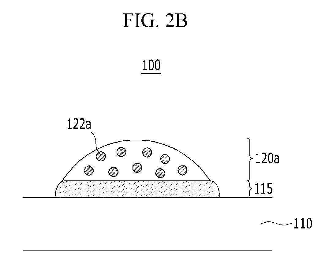
- FIG. 2A to FIG. 2D are cross-sectional views schematically illustrating a conductive structure including a conductive powder that forms a solid solution with and is diffused into a metallic glass when the conductive paste according to example embodiments is applied on a semiconductor substrate 110.
- a conductive structure 100 may include a conductive paste 120a applied on a semiconductor substrate 110.
- the conductive paste 120a may include a conductive powder 122a and a metallic glass 115a, which are each separately present as particles.
- Tg glass transition temperature
- the metallic glass 115a may soften and demonstrate liquid-like behavior.
- the softened metallic glass 115a may demonstrate wettability on the semiconductor substrate 110 to provide a buffer layer 115.
- the buffer layer 115 may closely contact a relatively wide area of semiconductor substrate 110.
- the conductive powder 122a may still be present as particles in the conductive paste 120a.
- the electrode prepared by using the conductive paste may include a buffer layer positioned at a region which is adjacent to the semiconductor substrate, and an electrode portion positioned at a region other than a region where the buffer layer is formed, for example, on the buffer layer.
- the conductive structure 100 when the conductive structure 100 is heated above the eutectic temperature of the conductive powder 122a and the metallic glass, the conductive powder 122a and the metallic glass enter a eutectic state, and a portion of the conductive powder 122a may form a solid solution with the metallic glass and diffuse into the buffer layer 115.
- a portion of the conductive powder 122a (see FIG. 1C ) diffused into the buffer layer 115 may be further diffused into the semiconductor substrate 110 and/or the interface of the semiconductor substrate 110 and buffer layer 115.
- the conductive powder may be recrystallized to provide a front electrode portion 120 including a first conductive powder 122b that is recrystallized, and the second conductive powder 122c that permeated into the semiconductor substrate 110 may also be recrystallized.
- a front electrode portion 120 formed with the first conductive powder 122b is provided, and a buffer layer 115 including metallic glass may be formed between the front electrode portion 120 and the semiconductor substrate 110.
- the second conductive powder 122c may be permeated into the semiconductor substrate 110 and recrystallized.
- the second conductive powder 122c present in the semiconductor substrate 110 may effectively transmit electrons produced in the semiconductor substrate 110 by solar light through the buffer layer 115 into the front electrode portion 120, and may simultaneously decrease the contact resistance between the semiconductor substrate 110 and the electrode portion 120 thereby reducing the electron loss and enhancing the efficiency of the solar cell.
- FIG. 3 is a cross-sectional view showing a solar cell according to example embodiments.
- front side refers to the side receiving solar energy
- rear side refers to the side opposite to the front side hereinafter.
- the solar cell 200 may include a semiconductor substrate 110 including a lower semiconductor layer 110a and an upper semiconductor layer 110b.
- the semiconductor substrate 110 may be formed of a crystalline silicon or compound semiconductor.
- the crystalline silicon may be, for example, a silicon wafer.
- One of the lower semiconductor layer 110a and the upper semiconductor layer 110b may be a semiconductor layer doped with a p-type impurity, and the other may be a semiconductor layer doped with an n-type impurity.
- the lower semiconductor layer 110a may be a semiconductor layer doped with a p-type impurity
- the upper semiconductor layer 110b may be a semiconductor layer doped with an n-type impurity.
- the p-type impurity may be a Group IIIA element, e.g., boron (B)
- the n-type impurity may be a Group VA element, e.g., phosphorus (P).
- the surface of the upper semiconductor layer 110b may be subjected to surface texturing.
- the surface-textured upper semiconductor layer 110b may have protrusions and depressions, e.g., in a pyramid shape, or a porous structure, e.g., a honeycomb shape.
- the surface-textured upper semiconductor layer 110b may have an enlarged surface area to enhance the light-absorption rate and decrease reflectivity, thereby improving efficiency of a solar cell.
- a plurality of front electrodes 123 may be disposed on the upper semiconductor layer 110b.
- the plurality of front electrodes 123 are arranged in parallel to the direction of the substrate 110, and may be designed in a grid pattern to reduce shadowing loss and sheet resistance.
- a front electrode of the plurality of front electrodes 123 may include a buffer layer 115 positioned at a region which is adjacent to the upper semiconductor layer 110b, and the front electrode portion 120 positioned at a region other than a region where the buffer layer 115 is formed.
- FIG. 3 shows that the buffer layer 115 is formed on the upper semiconductor layer 110b, but is not limited thereto.
- the buffer layer 115 may be omitted, or may be formed on a separate part of the upper semiconductor layer 110b.
- the front electrode may be disposed by a screen printing method using a conductive paste.
- the conductive paste is the same as described above.
- the front electrode portion 120 may be formed of a conductive material, for example, a low resistance conductive material such as at least one of silver (Ag), aluminum (Al), copper (Cu), nickel (Ni) and/or a combination thereof.
- a conductive material for example, a low resistance conductive material such as at least one of silver (Ag), aluminum (Al), copper (Cu), nickel (Ni) and/or a combination thereof.
- a conductive buffer layer 115 may be disposed between the upper semiconductor layer 110b and the front electrode portion 120.
- the conductive buffer layer 115 may have conductivity due to a metallic glass. Because the conductive buffer layer 115 has parts that contact the front electrode portion 120 and the upper semiconductor layer 110b, the conductive buffer layer 115 may decrease loss of electric charges by enlarging the path for transferring electric charges between the upper semiconductor layer 110b and the front electrode portion 120.
- the metallic glass in the conductive buffer layer 115 may be a component included in the conductive paste for the front electrode portion 120 and may be softened before the conductive material for the front electrode portion 120 during processing, so that the metallic glass may be disposed under the front electrode portion 120.
- the crystallized conductive powder 122d may be present in the buffer layer 115, the upper semiconductor layer 110b disposed under the buffer layer 115 and/or the interface of the upper semiconductor layer 110b and the buffer layer 115.
- the crystallized conductive powder 122d may be melted during the firing process to form a front electrode using the conductive paste, passed through the buffer layer 115, diffused into the upper semiconductor layer 110b, and crystallized.
- the crystallized conductive powder 122d may decrease the contact resistance between the upper semiconductor layer 110b and the front electrode portion 120 together with the buffer layer 115, and improve the electrical characteristics of the solar cell.
- a bus bar electrode (not shown) may be disposed on the front electrode portion 120.
- the bus bar electrode connects adjacent solar cells during assembly of a plurality of solar cells.
- a dielectric layer 130 may be disposed under the semiconductor substrate 110.
- the dielectric layer 130 may increase efficiency of a solar cell by preventing or inhibiting recombination of electric charges and leakage of a current.
- the dielectric layer 130 may include a plurality of through-holes 135, and the semiconductor substrate 110 and a rear electrode that will be described may contact through the through-holes 135.
- the dielectric layer 130 may be formed with at least one of silicon oxide (SiO 2 ), silicon nitride (SiN x ), aluminum oxide (Al 2 O 3 ), and a combination thereof, and may have a thickness of about 100 ⁇ to about 2000 ⁇ .
- the rear electrode 143 may be disposed under the dielectric layer 130.
- the rear electrode 143 may be formed of a conductive material, for example, an opaque metal such as aluminum (Al).
- the rear electrode 143 may be disposed by a screen printing method using a conductive paste in the same manner as the plurality of front electrodes 123.
- the rear electrode 143 may include a buffer layer 115 positioned at a region which is adjacent to the lower semiconductor layer 110a, and a rear electrode portion 140 positioned at a region other than a region where the buffer layer 115 is formed and including a conductive material in the same manner as the plurality of front electrodes.
- the buffer layer may be omitted, or may be formed on a separate part of the lower semiconductor layer 110a.
- the crystallized conductive powder 122d may be present in the buffer layer 115, the lower semiconductor layer 110a disposed on the buffer layer 115 and/or the interface of the lower semiconductor layer 110a.
- the crystallized conductive powder 122d may be melted during the firing process to form a rear electrode using the conductive paste, passed through the buffer layer 115, diffused into the lower semiconductor layer 110a, and crystallized.
- the crystallized conductive powder 122d may decrease the contact resistance between the lower semiconductor layer 110a and the rear electrode portion 140 together with the buffer layer 115, and improve the electrical characteristics of the solar cell.
- a semiconductor substrate 110 such as a silicon wafer is prepared.
- the semiconductor substrate 110 may be doped with a p-type impurity, as an example.
- the surface-texturing treatment may be performed by a wet method using a strong acid, e.g., nitric acid and hydrofluoric acid, or a strong base, e.g., sodium hydroxide, or by a dry method using plasma.
- a strong acid e.g., nitric acid and hydrofluoric acid
- a strong base e.g., sodium hydroxide
- the semiconductor substrate 110 may be doped with an n-type impurity, as an example.
- the n-type impurity may be doped by diffusing POCl 3 or H 3 PO 4 at a higher temperature.
- the semiconductor substrate 110 may include a lower semiconductor layer 110a and an upper semiconductor layer 110b doped with different impurities from each other.
- a conductive paste for a front electrode 123 may be applied on the upper semiconductor layer 110b.
- the conductive paste for a front electrode 123 may be provided by a screen printing method.
- the screen printing method includes applying the conductive paste including a conductive powder, a metallic glass, and an organic vehicle at the position where a front electrode 123 is to be positioned, and drying the same.
- the conductive paste may include a metallic glass, and the metallic glass may be prepared using any kind of method, e.g., melt spinning, infiltration casting, gas atomization, ion irradiation, or mechanical alloying.
- the conductive paste for a front electrode 123 is dried.
- a dielectric layer 130 may be provided by stacking aluminum oxide (Al 2 O 3 ) or silicon oxide (SiO 2 ) on the rear side of the semiconductor substrate 110, as an example, by a plasma enhanced chemical vapor deposition (PECVD) method.
- Al 2 O 3 aluminum oxide
- SiO 2 silicon oxide
- a plurality of through-holes 135 may be provided on one part of the dielectric layer 130 by an ablation with a laser.
- the conductive paste for a rear electrode 143 may be subsequently applied on one side of the dielectric layer 130 by a screen printing method.
- the conductive paste for a rear electrode 143 may then be dried.
- the conductive paste for a front electrode 123 and the conductive paste for a rear electrode 143 are co-fired. Alternatively, the conductive paste for a front electrode 123 and the conductive paste 143 for a rear electrode may be respectively fired.
- the firing may be performed at a higher temperature than the melting temperature of the conductive powder in a furnace, for example, at a temperature ranging from about 200°C to about 1000°C.
- FIG. 4 is a cross-sectional view showing a solar cell according to example embodiments.
- a solar cell 300 may include a semiconductor substrate 110 doped with a p-type or an n-type impurity.
- the semiconductor substrate 110 may include a plurality of first doping regions 111a and second doping regions 111b on the rear side and may be doped with different impurities from each other.
- the first doping regions 111a may be doped with an n-type impurity
- the second doping regions 111b may be doped with a p-type impurity.
- the first doping regions 111a and the second doping regions 111b may be alternately disposed on the rear side of the semiconductor substrate 110.
- the front side of the semiconductor substrate 110 may be surface-textured, and therefore may enhance the light-absorption rate and decrease the reflectivity, thereby improving efficiency of a solar cell.
- An insulation layer 112 may be provided on the semiconductor substrate 110.
- the insulation layer 112 may be formed of an insulating material that absorbs relatively little light, for example, at least one of silicon nitride (SiN x ), silicon oxide (SiO 2 ), titanium oxide (TiO 2 ), aluminum oxide (Al 2 O 3 ), magnesium oxide (MgO), cerium oxide (CeO 2 ), and/or a combination thereof.
- the insulation layer 112 may be a single layer or more than one layer.
- the insulation layer 112 may have a thickness ranging from about 200 ⁇ to about 1500 ⁇ .
- the insulation layer 112 may be an anti-reflective coating (ARC) that decreases the reflectivity of light and increases selectivity of a particular wavelength on the surface of the solar cell, and simultaneously improves contact characteristics with silicon at the surface of the semiconductor substrate 110, thereby increasing efficiency of the solar cell.
- ARC anti-reflective coating
- a dielectric layer 150 having a plurality of through-holes may be disposed on the rear side of the semiconductor substrate 110.
- a first electrode connected with the first doping region 111a and a second electrode connected with the second doping region 111b are disposed on the rear side of the semiconductor substrate 110, respectively.
- the first electrode and the first doping region 111a may contact each other through a through-hole (see FIG. 3 ), and the second electrode and the second doping region 111b may contact each other through a through-hole (see FIG. 3 ).
- the first electrode and the second electrode may be alternately disposed.
- the first electrode may include a buffer layer 115 positioned at a region which is adjacent to the first doping region 111a, and a first electrode portion 121 positioned at a region other than a region where the buffer layer 115 is formed.
- the second electrode may include a buffer layer 115 positioned at a region which is adjacent to the second doping region 111b, and a second electrode portion 141 positioned at a region other than a region where the buffer layer 115 is formed.
- the buffer layer 115 may be omitted, or may be formed on a region adjacent to the first doping region 111a, a region adjacent to the second doping region 111b, and/or a combination thereof.
- the first electrode and the second electrode are formed using a conductive paste including a conductive powder, a metallic glass, and an organic vehicle.
- the buffer layer 115 may be disposed between the first doping region 111a and the first electrode portion 121, and between the second doping region 111b and the second electrode portion 141.
- the buffer layer 115 may have conductivity due to a metallic glass. Because the conductive buffer layer 115 has portions contacting the first electrode portion 121 or the second electrode portion 141 and portions contacting the first doping region 111a or the second doping region 111b, undesirable loss of electric charges may decrease by enlarging the path for transferring charges between the first doping region 111a and the first electrode portion 121, or between the second doping region 111b and the second electrode portion 141.
- At least one of the buffer layer 115, the first doping region 111a, the second doping region 111b, the interface of the first doping region 111a and the buffer layer 115, and the interface of the second doping region 111b of the semiconductor substrate 110 and the buffer layer 115 includes a crystallized conductive powder 122d.
- the crystallized conductive powder 122d may be melted and passed through the buffer layer 115 and diffused into the first doping region 111a and/or the second doping region 111b of semiconductor substrate 110 during the baking process when the first electrode and/or the second electrode is provided using the conductive powder 122c, and crystallized.
- the crystallized conductive powder 122d may decrease the contact resistance between the first doping region 111a and the first electrode portion 121 and between the second doping region 111b and the second electrode portion 141 and improve the electrical characteristics of solar cell.
- the solar cell according to example embodiments including both the first electrode and the second electrode on the rear surface of the solar cell may decrease an area where a metal is positioned on the front surface, which may decrease shadowing loss and increase solar cell efficiency.
- a semiconductor substrate 110 doped with, for example, an n-type impurity is prepared.
- the semiconductor substrate 110 may be surface-textured, and an insulation layer 112 and a dielectric layer 150 may be disposed on the front side and the rear side of the semiconductor substrate 110, respectively.
- the insulation layer 112 and the dielectric layer 150 may be formed by chemical vapor deposition (CVD).
- the first doping region 111a and the second doping region 111b may be formed by sequentially doping a p-type impurity and an n-type impurity at a higher concentration on the rear side of the semiconductor substrate 110.
- a conductive paste for a first electrode may be applied on one side of the dielectric layer 150 corresponding to the first doping region 111a, and a conductive paste for a second electrode may be applied on the other side corresponding to the second doping region 111b.
- the conductive paste for a first electrode and the conductive paste for a second electrode may be provided by a screen printing method, and the conductive paste including the conductive powder, metallic glass, and organic vehicle described above may be respectively used.
- the conductive paste for a first electrode and the conductive paste for a second electrode may be fired together or respectively.
- the firing may be performed at a higher temperature than the melting temperature of a conductive powder in a furnace.
- the aforementioned conductive paste is illustrated as an example of being applied to an electrode for a solar cell, but is not limited thereto, and may be applied to an electrode for all electronic devices.
- a metallic glass of Cu 46 Zr 46 Al 8 is prepared in a form of a ribbon having a thickness of about 90 ⁇ m and a width of about 0.5cm.
- the metallic glass ribbon is cut to have a length of 1 cm and coated with silver (Ag) paste including 85wt% of silver (Ag).
- the metallic glass ribbon is heated at about 650°C for about 30 minutes while being exposed to air to provide a conductive thin film. The heating treatment is performed at a speed of about 50°C/min.
- a conductive thin film is provided on the metallic glass ribbon in accordance with the same procedure as in Example 1, except that the metallic glass is Cu 58 1 Zr 35 9 Al 6 instead of Cu 46 Zr 46 Al 8 .
- a conductive thin film is provided on the metallic glass ribbon in accordance with the same procedure as in Example 1, except that the metallic glass is Cu 50 Zr 50 instead of Cu 46 Zr 46 Al 8 .
- the metallic glass ribbons and the conductive thin films obtained from Examples 1 and 2 and Comparative Example 1 are cut and analyzed regarding the cross-sectional surface.
- Table 1 shows the solid solubility of silver (Ag) present in the metallic glass ribbon at a place apart from the interface of the metallic glass ribbon and the conductive thin film obtained from each of Examples 1 and 2 and Comparative Example 1 by about 3 ⁇ m.
- the solid solubility of silver (Ag) is determined by measuring the silver concentration (at%) in the interface of the metallic glass ribbon and the conductive thin film at a depth of about 3 ⁇ m through energy dispersive x-ray spectroscopy (EDS).
- EDS energy dispersive x-ray spectroscopy
- Example 1 including metallic glass having a relatively high amount of aluminum (Al) has a higher silver (Ag) solid-solubility than that of Example 2.
- Silver (Ag) powder and metallic glass of Cu 46 Zr 46 Al 8 are added into an organic vehicle including an ethyl cellulose binder and a butyl carbitol solvent.
- the silver (Ag) powder, the metallic glass of Cu 46 Zr 46 Al 8 , and the organic vehicle are mixed at about 84 wt%, about 4 wt%, and about 12 wt%, respectively, based on the total amount of conductive paste.
- the mixture is kneaded using a 3-roll mill to provide a conductive paste.
- the conductive paste is coated on a silicon wafer by a screen printing method, rapidly heated to about 500°C using a belt furnace, and slowly heated to about 900°C.
- the conductive paste is cooled to provide an electrode.
- a conductive paste is prepared in accordance with the same procedure as in Example 3 to provide an electrode, except that Cu 58 1 Zr 35 9 Al 6 is used as a metallic glass instead of Cu 46 Zr 46 Al 8 .
- a conductive paste is prepared in accordance with the same procedure as in Example 3 to provide an electrode, except that Cu 50 Zr 50 is used as a metallic glass instead of Cu 46 Zr 46 Al 8 .
- Each contact resistance of electrodes obtained from Examples 3 and 4 is compared to that of Comparative Example 2.
- the contact resistance is determined by a transfer length method (TLM).
- Table 2 shows the contact resistance of each electrode obtained from Examples 3 and 4 and Comparative Example 2. (Table 2) Contact resistance (m ⁇ cm 2 ) Example 3 35.60 Example 4 40.07 Comparative Example 2 60.57
- the electrodes obtained from Examples 3 and 4 have lower contact resistance than the electrode obtained from Comparative Example 2. Thereby, the contact resistance is decreased by using a metallic glass including aluminum (Al) that is capable of providing a solid-solution with silver (Ag). In addition, the contact resistance is further decreased by using a metallic glass having an increased amount of aluminum (Al) to further increase the solid-solubility with silver (Ag).
- a metallic glass including aluminum (Al) that is capable of providing a solid-solution with silver (Ag).
- the contact resistance is further decreased by using a metallic glass having an increased amount of aluminum (Al) to further increase the solid-solubility with silver (Ag).
Landscapes
- Chemical & Material Sciences (AREA)
- Engineering & Computer Science (AREA)
- Mechanical Engineering (AREA)
- Materials Engineering (AREA)
- Metallurgy (AREA)
- Organic Chemistry (AREA)
- Physics & Mathematics (AREA)
- Dispersion Chemistry (AREA)
- Spectroscopy & Molecular Physics (AREA)
- Photovoltaic Devices (AREA)
- Conductive Materials (AREA)
- Life Sciences & Earth Sciences (AREA)
- Sustainable Development (AREA)
- Sustainable Energy (AREA)
Abstract


Description
- Example embodiments relate to a conductive paste, and an electronic device and a solar cell including an electrode formed using the conductive paste.
- A solar cell is a photoelectric conversion device that transforms solar energy into electrical energy. Solar cells have attracted attention as a potentially infinite and pollution-free next generation energy source.
- A solar cell includes p-type and n-type semiconductors, When an electron-hole pair ("EHP") is produced by light absorbed in a photoactive layer of the semiconductors, the solar cell produces electrical energy by transferring electrons and holes to the n-type and p-type semiconductors, respectively, and then collecting the electrons and holes in electrodes of the solar cell.
- A solar cell should desirably have the highest possible efficiency for producing electrical energy from solar energy. In order to improve this efficiency, the solar cell desirably absorbs light with minor loss so that the solar cell may produce as many electron-hole pairs as possible, and collect the produced charges.
- Further, an electrode of a solar cell may be manufactured in a screen-printing method using a conductive paste.
- Example embodiments provide a conductive paste which is capable of reducing charge loss and improving efficiency of a solar cell. Example embodiments also provide an electronic device including an electrode having the conductive paste.
- Example embodiments also provide a solar cell including an electrode including a product of the conductive paste.
- According to example embodiments, a conductive paste may include a conductive powder, a metallic glass including a first element having a heat of mixing value with the conductive powder of less than 0, and an organic vehicle.
- The eutectic temperature of the conductive powder and the first element may be lower than a firing temperature of the conductive paste. The firing temperature of the conductive paste may be about 1000°C or lower. The firing temperature of the conductive paste may range from about 200 to about 1000°C.
- The first element may include at least one of lanthanum (La), cerium (Ce), praseodymium (Pr), promethium (Pm), samarium (Sm), lutetium (Lu), yttrium (Y), neodymium (Nd), gadolinium (Gd), terbium (Tb), dysprosium (Dy), holmium (Ho), erbium (Er), thulium (Tm), thorium (Th), calcium (Ca), scandium (Sc), barium (Ba), beryllium (Be), bismuth (Bi), germanium (Ge), lead (Pb), ytterbium (Yb), strontium (Sr), europium (Eu), zirconium (Zr), thallium (TI), lithium (Li), hafnium (Hf), magnesium (Mg), phosphorus (P), arsenic (As), palladium (Pd), gold (Au), plutonium (Pu), gallium (Ga), aluminum (Al), copper (Cu), zinc (Zn), antimony (Sb), silicon (Si), tin (Sn), titanium (Ti), cadmium (Cd), indium (In), platinum (Pt), and mercury (Hg).
- The metallic glass may further include a second element and a third element, and the metallic glass may be an alloy having a composition represented by the following Chemical Formula 1:
Ax-By-Cz [Chemical Formula 1]
wherein A, B, and C are the first element, the second element, and the third element, respectively; x, y, and z are composition ratios of the first element, the second element, and the third element, respectively; and x+y+z=100. - The first element, the second element, and the third element may be included in a ratio satisfying the following Equation 1:

- The metallic glass may further include a second element, a third element, and a fourth element, and the metallic glass may be an alloy having a composition represented by the following Chemical Formula 2:
Ax-By-Cz-Dw [Chemical Formula 2]
wherein A, B, C, and D are the first element, the second element, the third element, and the fourth element, respectively; x, y, z, and w are composition ratios of the first element, the second element, the third element, and the fourth element, respectively; and x+y+z+w=100. - The first element, the second element, the third element, and the fourth element may be included in a ratio satisfying the following Equation 2:

wherein ΔH1 is a heat of mixing value for the first element and the second element, ΔH2 is a heat of mixing value for the second element and the third element, ΔH3 is a heat of mixing value for the third element and the fourth element, ΔH4 is a heat of mixing value for the fourth element and the first element, ΔH5 is a heat of mixing value for the first element and the third element, and ΔH6 is a heat of mixing value for the second element and the third element. - The conductive powder may have resistivity of about 100µΩcm or less. The conductive powder may include at least one of silver (Ag), aluminum (Al), copper (Cu), nickel (Ni), and a combination thereof. The conductive powder, the metallic glass, and the organic vehicle may be included at about 30 to 99wt%, about 0.1 to 20wt%, and about 0.9 to 69.9wt%, respectively, based on the total amount of conductive paste.
- According to example embodiments, an electronic device may include an electrode formed using the conductive paste. The conductive paste includes a conductive powder, a metallic glass including a first element having a heat of mixing value with the conductive powder of less than 0, and an organic vehicle.
- According to example embodiments, a solar cell may include an electrode electrically connected with a semiconductor layer. The electrode may be formed using the conductive paste of example embodiments.
- The electrode may include a buffer layer at a region adjacent to the semiconductor layer, and an electrode portion at another region different from the region where the buffer layer is formed. At least one of the buffer layer, the interface of the semiconductor layer and the buffer layer, and the semiconductor layer includes the conductive material that is crystallized.
- The eutectic temperature of the conductive powder and the first element may be lower than the firing temperature of the conductive paste. The conductive paste may have a firing temperature of less than about 1000°C.
- The first element may include at least one of lanthanum (La), cerium (Ce), praseodymium (Pr), promethium (Pm), samarium (Sm), lutetium (Lu), yttrium (Y), neodymium (Nd), gadolinium (Gd), terbium (Tb), dysprosium (Dy), holmium (Ho), erbium (Er), thulium (Tm), thorium (Th), calcium (Ca), scandium (Sc), barium (Ba), beryllium (Be), bismuth (Bi), germanium (Ge), lead (Pb), ytterbium (Yb), strontium (Sr), europium (Eu), zirconium (Zr), thallium (TI), lithium (Li), hafnium (Hf), magnesium (Mg), phosphorus (P), arsenic (As), palladium (Pd), gold (Au), plutonium (Pu), gallium (Ga), aluminum (Al), copper (Cu), zinc (Zn), antimony (Sb), silicon (Si), tin (Sn), titanium (Ti), cadmium (Cd), indium (In), platinum (Pt), and mercury (Hg).
- The metallic glass may further include a second element and a third element, and the metallic glass may be an alloy having a composition represented by the following Chemical Formula 1:
Ax-By-Cz [Chemical Formula 1]
- In the Chemical Formula 1, A, B, and C are the first element, the second element, and the third element, respectively; x, y, and z are the composition ratios of the first element, the second element, and the third element, respectively; and x+y+z=100.
- The first element, the second element, and the third element may be included in a ratio satisfying the following Equation 1:

- In Equation 1, ΔH1 is a heat of mixing value for the first element and the second element, ΔH2 is a heat of mixing value for the second element and the third element, and ΔH3 is a heat of mixing value for the third element and the first element.
- The metallic glass may further include a second element, a third element, and a fourth element, and the metallic glass may be an alloy having a composition represented by the following Chemical Formula 2:
Ax-By-Cz-Dw [Chemical Formula 2]
- In the Chemical Formula 2, A, B, C, and D are the first element, the second element, the third element, and the fourth element, respectively; x, y, z, and w are the composition ratios of the first element, the second element, the third element, and the fourth element, respectively; and x+y+z+w=100.
- The first element, the second element, the third element, and the fourth element may be included in a ratio satisfying the following Equation 2:

- In Equation 2, ΔH1 is a heat of mixing value for the first element and the second element, ΔH2 is a heat of mixing value for the second element and the third element, ΔH3 is a heat of mixing value for the third element and the fourth element, ΔH4 is a heat of mixing value for the fourth element and the first element, ΔH5 is a heat of mixing value for the first element and the third element, and ΔH6 is a heat of mixing value for the second element and the third element.
- The conductive powder may have a resistivity ranging from about 100µΩcm or less. The conductive powder may include at least one of silver (Ag), aluminum (Al), copper (Cu), nickel (Ni), and a combination thereof.
- These and/or other aspects will become apparent and more readily appreciated from the following description of example embodiments, taken in conjunction with the accompanying drawings of which:
-
FIG. 1 is a schematic view showing a heat of mixing value for a ternary alloy according to example embodiments including Al-Cu-Zr depending upon the ratio of each element. -
FIG. 2A to FIG. 2D are cross-sectional views schematically illustrating a conductive structure according to example embodiments including a conductive powder that forms a solid solution with and is diffused into a metallic glass. -
FIGS. 3-4 are cross-sectional views illustrating a solar cell according to example embodiments. - Example embodiments will hereinafter be described in detail, and may be easily performed by those who have common knowledge in the related art. This disclosure may, however, be embodied in many different forms and should not be construed as limited to example embodiments set forth herein.
- In the drawings, the thickness of layers, films, panels, regions, etc., are exaggerated for clarity. Like reference numerals designate like elements throughout the specification. It will be understood that when an element such as a layer, film, region, or substrate is referred to as being "on" another element, it can be directly on the other element or intervening elements may also be present. In contrast, when an element is referred to as being "directly on" another element, there are no intervening elements present.
- It will be understood that, although the terms "first", "second", etc. may be used herein to describe various elements, components, regions, layers and/or sections, these elements, components, regions, layers and/or sections should not be limited by these terms. These terms are only used to distinguish one element, component, region, layer or section from another element, component, region, layer or section. Thus, a first element, component, region, layer or section discussed below could be termed a second element, component, region, layer or section without departing from the teachings of example embodiments.
- Spatially relative terms, such as "beneath," "below," "lower," "above," "upper" and the like, may be used herein for ease of description to describe one element or feature's relationship to another element(s) or feature(s) as illustrated in the figures. It will be understood that the spatially relative terms are intended to encompass different orientations of the device in use or operation in addition to the orientation depicted in the figures. For example, if the device in the figures is turned over, elements described as "below" or "beneath" other elements or features would then be oriented "above" the other elements or features. Thus, the exemplary term "below" can encompass both an orientation of above and below. The device may be otherwise oriented (rotated 90 degrees or at other orientations) and the spatially relative descriptors used herein interpreted accordingly.
- The terminology used herein is for the purpose of describing particular embodiments only and is not intended to be limiting of example embodiments. As used herein, the singular forms "a," "an" and "the" are intended to include the plural forms as well, unless the context clearly indicates otherwise. It will be further understood that the terms "comprises" and/or "comprising," when used in this specification, specify the presence of stated features, integers, steps, operations, elements, and/or components, but do not preclude the presence or addition of one or more other features, integers, steps, operations, elements, components, and/or groups thereof.
- Example embodiments are described herein with reference to cross-sectional illustrations that are schematic illustrations of idealized embodiments (and intermediate structures) of example embodiments. As such, variations from the shapes of the illustrations as a result, for example, of manufacturing techniques and/or tolerances, are to be expected. Thus, example embodiments should not be construed as limited to the particular shapes of regions illustrated herein but are to include deviations in shapes that result, for example, from manufacturing. For example, an implanted region illustrated as a rectangle will, typically, have rounded or curved features and/or a gradient of implant concentration at its edges rather than a binary change from implanted to non-implanted region. Likewise, a buried region formed by implantation may result in some implantation in the region between the buried region and the surface through which the implantation takes place. Thus, the regions illustrated in the figures are schematic in nature and their shapes are not intended to illustrate the actual shape of a region of a device and are not intended to limit the scope of example embodiments.
- Unless otherwise defined, all terms (including technical and scientific terms) used herein have the same meaning as commonly understood by one of ordinary skill in the art to which example embodiments belong. It will be further understood that terms, such as those defined in commonly-used dictionaries, should be interpreted as having a meaning that is consistent with their meaning in the context of the relevant art and will not be interpreted in an idealized or overly formal sense unless expressly so defined herein. Hereinafter, the term 'element' refers to a metal and a semimetal.
- A conductive paste according to example embodiments includes a conductive powder, a metallic glass including a first element having a heat of mixing value of less than 0 with the conductive powder, and an organic vehicle.
- The conductive powder may be selected from the metal having a resistivity of about 100µΩcm or less. The conductive powder may be, for example, at least one of a silver (Ag)-containing metal, e.g., silver or a silver alloy, an aluminum (Al)-containing metal, e.g., aluminum or an aluminum alloy, a copper (Cu)-containing metal, e.g., copper (Cu) or a copper alloy, a nickel (Ni)-containing metal, e.g., nickel (Ni) or a nickel alloy, and a combination thereof. However, example embodiments are not limited thereto, and may be a different kind of metal or may include an additive other than the metal.
- The conductive powder may have a particle size (e.g., average particle size) ranging from about 1 nm to about 50µm, for example, about 0.1 to about 50µm. The conductive powder may also have a particle size ranging from about 0.5 to about 40 µm, for example, about 1 to about 30µm.
- The metallic glass may include an alloy having a disordered atomic structure including two or more elements. The metallic glass may be an amorphous metal. Because the metallic glass has a relatively low resistance, which is different from an insulating glass, e.g., a silicate, the metallic glass may be an electrical conductor at a voltage and a current of a solar cell.
- The metallic glass may include a first element having a heat of mixing value of less than 0 with the conductive powder. The heat of mixing value of less than 0 means that two materials may be thermodynamically mixed spontaneously when they are in a melted state. What the heat of mixing value for the conductive powder and the first element being less than 0 means is that the conductive powder and the first element may spontaneously form a solid solution in a melted state.
- When the eutectic temperature of the conductive powder and the first element is lower than the firing temperature of the conductive paste, the conductive powder and the first element may be in a melted state while firing the conductive paste, and the melted conductive powder may be solid-dissolved and diffused into the first element in a melted state.
- The conductive paste may have a firing temperature of about 1000°C or lower, for example, of about 200°C to about 1000°C, so the metallic glass may be selected from elements capable of providing a eutectic state with the conductive powder within the temperature range.
- For example, when the conductive powder is a silver (Ag)-containing metal, the first element capable of providing a solid solution with the conductive powder at about 1000°C or lower may be at least one of lanthanum (La), cerium (Ce), praseodymium (Pr), promethium (Pm), samarium (Sm), lutetium (Lu), yttrium (Y), neodymium (Nd), gadolinium (Gd), terbium (Tb), dysprosium (Dy), holmium (Ho), erbium (Er), thulium (Tm), thorium (Th), calcium (Ca), scandium (Sc), barium (Ba), beryllium (Be), bismuth (Bi), germanium (Ge), lead (Pb), ytterbium (Yb), strontium (Sr), europium (Eu), zirconium (Zr), thallium (TI), lithium (Li), hafnium (Hf), magnesium (Mg), phosphorus (P), arsenic (As), palladium (Pd), gold (Au), plutonium (Pu), gallium (Ga), aluminum (Al), copper (Cu), zinc (Zn), antimony (Sb), silicon (Si), tin (Sn), titanium (Ti), cadmium (Cd), indium (In), platinum (Pt), and mercury (Hg).
- The conductive powder may be a silver (Ag)-containing metal, but example embodiments are not limited thereto. The conductive powder may be selected from various elements when other metals are included.
- The metallic glass may be a ternary alloy further including a second element and a third element other than the first element.
- When the metallic glass is a ternary alloy, the ternary alloy may be represented by the Chemical Formula 1.
Ax-By-Cz Chemical Formula 1]
- In the Chemical Formula 1, A, B, and C are the first element, the second element, and the third element, respectively; x, y, and z are the composition ratios of the first element, the second element, and the third element, respectively; and x+y+z=100.
- In the composition of the metallic glass, the composition ratio of the first element for increasing the solid solubility of the conductive powder may be determined in the ratio for satisfying the following Equation 1.

- In the Equation 1, ΔH1 is a heat of mixing value for the first element and the second element; ΔH2 is a heat of mixing value for the second element and the third element; and ΔH3 is a heat of mixing value for the third element and the first element.
- As in Equation 1, when the total heat of mixing value of the metallic glass is less than 0, the composition of the metallic glass is thermodynamically stabilized, so as to determine the ratio (x) of the amount of the first element for increasing the solid solubility within the range.
- The metallic glass may be an alloy including at least two elements. For example, the first element may be aluminum (Al), and the second element and the third element may be copper (Cu) and zirconium (Zr), respectively.
- When the metallic glass is a ternary alloy including Al, Cu, and Zr in x%, y%, and z%, respectively, and when the heat of mixing value for Al-Cu is ΔH1, the heat of mixing value for Cu-Zr is ΔH2 and the heat of mixing value for Zr-Al is ΔH3, and the amount of the first element of Al may be determined within the range to provide the total heat of mixing value for metallic glasses of xyΔH1 + yzΔH2 + zxΔH3 to be less than 0.
-
FIG. 1 is a schematic view showing a heat of mixing value for a ternary alloy according to example embodiments including Al-Cu-Zr depending upon the ratio of amount of each element. - Referring to
FIG. 1 , the region A is a region having a heat of mixing value that satisfies -10≤xyΔH1 + yzΔH2 + zxΔH3≤-6; the region B is a region having a heat of mixing value that satisfies -6≤xyΔH1 + yzΔH2 + zxΔH3:≤-3; and the region C is a region having a heat of mixing value that satisfies -3≤xyΔH1 + yzΔH2 + zxΔH3<0. - The values x, y, and z may be determined within the range to provide a suitable total heat of mixing value referring to
FIG. 1 . - The metallic glass may be, for example, Cu58.1Zr35.9Al6 and Cu46Zr46Al8.
- The metallic glass may be a quaternary alloy further including a second element, a third element, and a fourth element other than the first element.
- When the metallic glass is a quaternary alloy, the metallic glass may be represented by the Chemical Formula 2.
Ax-By-Cz-Dw [Chemical Formula 2]
- In the Chemical Formula 2, A, B, C, and D are the first element, the second element, the third element, and the fourth element, respectively; x, y, z, and w are the composition ratios of the first element, the second element, the third element, and the fourth element, respectively; and x+y+z+w=1 00.
- In the composition of the metallic glass, the composition ratio of the first element for increasing the solid solubility of the conductive powder may be determined in the ratio for satisfying the following Equation 2.

- In the Equation 2, ΔH1 is a heat of mixing value for the first element and the second element; ΔH2 is a heat of mixing value for the second element and the third element; ΔH3 is a heat of mixing value for the third element and the fourth element; ΔH4 is a heat of mixing value for the fourth element and the first element, and ΔH5 is a heat of mixing value for the first element and the third element, and ΔH6 is a heat of mixing value for the second element and the third element..
- As in Equation 2, when the total heat of mixing value of the metallic glass is less than 0, the composition of the metallic glass is thermodynamically stabilized, so as to determine the ratio (x) of the amount of the first element for increasing the solid solubility within the range.
- The metallic glass may be an alloy including at least two elements. For example, the first element may be aluminum (Al), and the second element, the third element, and the fourth element may be copper (Cu), zirconium (Zr), and beryllium (Be), respectively.
- When the metallic glass is a quaternary alloy including Al, Cu, Zr, and Be in x%, y%, z%, and w%, respectively, and when the heat of mixing value for Al-Cu is ΔH1, the heat of mixing value for Cu-Zr is ΔH2, the heat of mixing value for Zr-Be is ΔH3, and the heat of mixing value for Be-Al is ΔH4, and the amount of the first element of Δl may be determined within the range to provide the total heat of mixing value for metallic glasses of xyΔH1 + yzΔH2 + zwΔH3 + wxΔH4 to be less than 0.
- The metallic glass may be, for example, Cu45Zr45Al8Be2.
- The organic vehicle may include an organic compound and a solvent. The organic compound may be contacted (e.g., mixed) with the conductive powder and the metallic glass to impart viscosity. The solvent may dissolve or suspend the foregoing components.
- The organic compound may include, for example, at least one selected from a (meth)acrylate; a cellulose, e.g., ethyl cellulose; a phenol; an alcohol; a tetrafluoroethylene (e.g., TEFLON®); and a combination thereof, and may further include an additive, e.g., a surfactant, a thickener, or a stabilizer, or a combination thereof.
- The solvent may be any solvent which is capable of dissolving or suspending any of the above compounds and may include, for example, at least one selected from terpineol, butylcarbitol, butylcarbitol acetate, pentanediol, dipentyne, limonene, ethyleneglycol alkylether, diethyleneglycol alkylether, ethyleneglycol alkylether acetate, diethyleneglycol alkylether acetate, diethyleneglycol dialkylether, triethyleneglycol alkylether acetate, triethylene glycol alkylether, propyleneglycol alkylether, propyleneglycol phenylether, dipropyleneglycol alkylether, tripropyleneglycol alkylether, propyleneglycol alkylether acetate, dipropyleneglycol alkylether acetate, tripropyleneglycol alkyl ether acetate, dimethyl phthalate, diethyl phthalate, dibutyl phthalate, and/or desalted water.
- The conductive powder, the metallic glass, and organic vehicle may be included in amounts of about 30wt% to about 99wt%, about 0.1wt% to about 20wt%, and about 0.9wt% to about 69.9wt%, based on the total amount of the conductive paste, respectively.
- The conductive paste may be diposed by screen-printing to provide an electrode for an electronic device. When the electrode is obtained by applying the conductive paste, for example, on the semiconductor substrate, the conductive powder may form a solid solution with the metallic glass including the first element and may diffuse into the melted metal glass as described below with reference to
FIG. 2A to FIG. 2D . -
FIG. 2A to FIG. 2D are cross-sectional views schematically illustrating a conductive structure including a conductive powder that forms a solid solution with and is diffused into a metallic glass when the conductive paste according to example embodiments is applied on asemiconductor substrate 110. - Referring to
FIG. 2A , aconductive structure 100 may include aconductive paste 120a applied on asemiconductor substrate 110. Theconductive paste 120a may include aconductive powder 122a and ametallic glass 115a, which are each separately present as particles. Referring toFIG. 2B , when theconductive structure 100 is heated above the glass transition temperature (Tg) of themetallic glass 115a, themetallic glass 115a may soften and demonstrate liquid-like behavior. The softenedmetallic glass 115a may demonstrate wettability on thesemiconductor substrate 110 to provide abuffer layer 115. Thebuffer layer 115 may closely contact a relatively wide area ofsemiconductor substrate 110. Because themetallic glass 115a has a lower glass transition temperature (Tg) than the sintering temperature of theconductive powder 122a, theconductive powder 122a may still be present as particles in theconductive paste 120a. Thereby, the electrode prepared by using the conductive paste may include a buffer layer positioned at a region which is adjacent to the semiconductor substrate, and an electrode portion positioned at a region other than a region where the buffer layer is formed, for example, on the buffer layer. - Referring to
FIG. 2C , when theconductive structure 100 is heated above the eutectic temperature of theconductive powder 122a and the metallic glass, theconductive powder 122a and the metallic glass enter a eutectic state, and a portion of theconductive powder 122a may form a solid solution with the metallic glass and diffuse into thebuffer layer 115. - Referring to
FIG. 2D , a portion of theconductive powder 122a (seeFIG. 1C ) diffused into thebuffer layer 115 may be further diffused into thesemiconductor substrate 110 and/or the interface of thesemiconductor substrate 110 andbuffer layer 115. When cooling thesemiconductor substrate 110, the conductive powder may be recrystallized to provide afront electrode portion 120 including a firstconductive powder 122b that is recrystallized, and the secondconductive powder 122c that permeated into thesemiconductor substrate 110 may also be recrystallized. Accordingly, afront electrode portion 120 formed with the firstconductive powder 122b is provided, and abuffer layer 115 including metallic glass may be formed between thefront electrode portion 120 and thesemiconductor substrate 110. The secondconductive powder 122c may be permeated into thesemiconductor substrate 110 and recrystallized. - The second
conductive powder 122c present in thesemiconductor substrate 110 may effectively transmit electrons produced in thesemiconductor substrate 110 by solar light through thebuffer layer 115 into thefront electrode portion 120, and may simultaneously decrease the contact resistance between thesemiconductor substrate 110 and theelectrode portion 120 thereby reducing the electron loss and enhancing the efficiency of the solar cell. - Referring to
FIG. 3 , the solar cell according to example embodiments is described.FIG. 3 is a cross-sectional view showing a solar cell according to example embodiments. - In the drawings, the thickness of layers, films, panels, regions, etc., are exaggerated for clarity. Like reference numerals designate like elements throughout the specification. It will be understood that when an element such as a layer, film, region, or substrate is referred to as being "on" another element, it can be directly on the other element or intervening elements may also be present. In contrast, when an element is referred to as being "directly on" another element, there are no intervening elements present.
- Hereinafter, for the better understanding and ease of description, the upper and lower positional relationship is described with respect to a
semiconductor substrate 110, but is not limited thereto. In addition, "front side" refers to the side receiving solar energy, and "rear side" refers to the side opposite to the front side hereinafter. - Referring to
FIG. 3 , thesolar cell 200 according to example embodiments may include asemiconductor substrate 110 including alower semiconductor layer 110a and anupper semiconductor layer 110b. - The
semiconductor substrate 110 may be formed of a crystalline silicon or compound semiconductor. The crystalline silicon may be, for example, a silicon wafer. One of thelower semiconductor layer 110a and theupper semiconductor layer 110b may be a semiconductor layer doped with a p-type impurity, and the other may be a semiconductor layer doped with an n-type impurity. For example, thelower semiconductor layer 110a may be a semiconductor layer doped with a p-type impurity, and theupper semiconductor layer 110b may be a semiconductor layer doped with an n-type impurity. Herein, the p-type impurity may be a Group IIIA element, e.g., boron (B), and the n-type impurity may be a Group VA element, e.g., phosphorus (P). - The surface of the
upper semiconductor layer 110b may be subjected to surface texturing. The surface-texturedupper semiconductor layer 110b may have protrusions and depressions, e.g., in a pyramid shape, or a porous structure, e.g., a honeycomb shape. The surface-texturedupper semiconductor layer 110b may have an enlarged surface area to enhance the light-absorption rate and decrease reflectivity, thereby improving efficiency of a solar cell. - A plurality of
front electrodes 123 may be disposed on theupper semiconductor layer 110b. The plurality offront electrodes 123 are arranged in parallel to the direction of thesubstrate 110, and may be designed in a grid pattern to reduce shadowing loss and sheet resistance. - A front electrode of the plurality of
front electrodes 123 may include abuffer layer 115 positioned at a region which is adjacent to theupper semiconductor layer 110b, and thefront electrode portion 120 positioned at a region other than a region where thebuffer layer 115 is formed.FIG. 3 shows that thebuffer layer 115 is formed on theupper semiconductor layer 110b, but is not limited thereto. Thebuffer layer 115 may be omitted, or may be formed on a separate part of theupper semiconductor layer 110b. - The front electrode may be disposed by a screen printing method using a conductive paste. The conductive paste is the same as described above.
- The
front electrode portion 120 may be formed of a conductive material, for example, a low resistance conductive material such as at least one of silver (Ag), aluminum (Al), copper (Cu), nickel (Ni) and/or a combination thereof. - A
conductive buffer layer 115 may be disposed between theupper semiconductor layer 110b and thefront electrode portion 120. Theconductive buffer layer 115 may have conductivity due to a metallic glass. Because theconductive buffer layer 115 has parts that contact thefront electrode portion 120 and theupper semiconductor layer 110b, theconductive buffer layer 115 may decrease loss of electric charges by enlarging the path for transferring electric charges between theupper semiconductor layer 110b and thefront electrode portion 120. - The metallic glass in the
conductive buffer layer 115 may be a component included in the conductive paste for thefront electrode portion 120 and may be softened before the conductive material for thefront electrode portion 120 during processing, so that the metallic glass may be disposed under thefront electrode portion 120. - The crystallized
conductive powder 122d may be present in thebuffer layer 115, theupper semiconductor layer 110b disposed under thebuffer layer 115 and/or the interface of theupper semiconductor layer 110b and thebuffer layer 115. The crystallizedconductive powder 122d may be melted during the firing process to form a front electrode using the conductive paste, passed through thebuffer layer 115, diffused into theupper semiconductor layer 110b, and crystallized. The crystallizedconductive powder 122d may decrease the contact resistance between theupper semiconductor layer 110b and thefront electrode portion 120 together with thebuffer layer 115, and improve the electrical characteristics of the solar cell. - A bus bar electrode (not shown) may be disposed on the
front electrode portion 120. The bus bar electrode connects adjacent solar cells during assembly of a plurality of solar cells. - A
dielectric layer 130 may be disposed under thesemiconductor substrate 110. Thedielectric layer 130 may increase efficiency of a solar cell by preventing or inhibiting recombination of electric charges and leakage of a current. Thedielectric layer 130 may include a plurality of through-holes 135, and thesemiconductor substrate 110 and a rear electrode that will be described may contact through the through-holes 135. - The
dielectric layer 130 may be formed with at least one of silicon oxide (SiO2), silicon nitride (SiNx), aluminum oxide (Al2O3), and a combination thereof, and may have a thickness of about 100Å to about 2000Å. - The
rear electrode 143 may be disposed under thedielectric layer 130. Therear electrode 143 may be formed of a conductive material, for example, an opaque metal such as aluminum (Al). Therear electrode 143 may be disposed by a screen printing method using a conductive paste in the same manner as the plurality offront electrodes 123. - The
rear electrode 143 may include abuffer layer 115 positioned at a region which is adjacent to thelower semiconductor layer 110a, and arear electrode portion 140 positioned at a region other than a region where thebuffer layer 115 is formed and including a conductive material in the same manner as the plurality of front electrodes. However, example embodiments are not limited thereto. The buffer layer may be omitted, or may be formed on a separate part of thelower semiconductor layer 110a. - The crystallized
conductive powder 122d may be present in thebuffer layer 115, thelower semiconductor layer 110a disposed on thebuffer layer 115 and/or the interface of thelower semiconductor layer 110a. The crystallizedconductive powder 122d may be melted during the firing process to form a rear electrode using the conductive paste, passed through thebuffer layer 115, diffused into thelower semiconductor layer 110a, and crystallized. The crystallizedconductive powder 122d may decrease the contact resistance between thelower semiconductor layer 110a and therear electrode portion 140 together with thebuffer layer 115, and improve the electrical characteristics of the solar cell. - Hereinafter, a method of manufacturing the solar cell is described with reference to
FIG. 3 . Asemiconductor substrate 110 such as a silicon wafer is prepared. Thesemiconductor substrate 110 may be doped with a p-type impurity, as an example. - Then the
semiconductor substrate 110 is subjected to a surface texturing treatment. The surface-texturing treatment may be performed by a wet method using a strong acid, e.g., nitric acid and hydrofluoric acid, or a strong base, e.g., sodium hydroxide, or by a dry method using plasma. - The
semiconductor substrate 110 may be doped with an n-type impurity, as an example. The n-type impurity may be doped by diffusing POCl3 or H3PO4 at a higher temperature. Thus, thesemiconductor substrate 110 may include alower semiconductor layer 110a and anupper semiconductor layer 110b doped with different impurities from each other. - A conductive paste for a
front electrode 123 may be applied on theupper semiconductor layer 110b. The conductive paste for afront electrode 123 may be provided by a screen printing method. The screen printing method includes applying the conductive paste including a conductive powder, a metallic glass, and an organic vehicle at the position where afront electrode 123 is to be positioned, and drying the same. - As described above, the conductive paste may include a metallic glass, and the metallic glass may be prepared using any kind of method, e.g., melt spinning, infiltration casting, gas atomization, ion irradiation, or mechanical alloying. The conductive paste for a
front electrode 123 is dried. - A
dielectric layer 130 may be provided by stacking aluminum oxide (Al2O3) or silicon oxide (SiO2) on the rear side of thesemiconductor substrate 110, as an example, by a plasma enhanced chemical vapor deposition (PECVD) method. - A plurality of through-
holes 135 may be provided on one part of thedielectric layer 130 by an ablation with a laser. - The conductive paste for a
rear electrode 143 may be subsequently applied on one side of thedielectric layer 130 by a screen printing method. The conductive paste for arear electrode 143 may then be dried. - The conductive paste for a
front electrode 123 and the conductive paste for arear electrode 143 are co-fired. Alternatively, the conductive paste for afront electrode 123 and theconductive paste 143 for a rear electrode may be respectively fired. - The firing may be performed at a higher temperature than the melting temperature of the conductive powder in a furnace, for example, at a temperature ranging from about 200°C to about 1000°C.
- Hereinafter, a solar cell according to example embodiments is described referring to
FIG. 4. FIG. 4 is a cross-sectional view showing a solar cell according to example embodiments. - A
solar cell 300 according to example embodiments may include asemiconductor substrate 110 doped with a p-type or an n-type impurity. Thesemiconductor substrate 110 may include a plurality offirst doping regions 111a andsecond doping regions 111b on the rear side and may be doped with different impurities from each other. For example, thefirst doping regions 111a may be doped with an n-type impurity, and thesecond doping regions 111b may be doped with a p-type impurity. Thefirst doping regions 111a and thesecond doping regions 111b may be alternately disposed on the rear side of thesemiconductor substrate 110. - The front side of the
semiconductor substrate 110 may be surface-textured, and therefore may enhance the light-absorption rate and decrease the reflectivity, thereby improving efficiency of a solar cell. - An
insulation layer 112 may be provided on thesemiconductor substrate 110. Theinsulation layer 112 may be formed of an insulating material that absorbs relatively little light, for example, at least one of silicon nitride (SiNx), silicon oxide (SiO2), titanium oxide (TiO2), aluminum oxide (Al2O3), magnesium oxide (MgO), cerium oxide (CeO2), and/or a combination thereof. Theinsulation layer 112 may be a single layer or more than one layer. Theinsulation layer 112 may have a thickness ranging from about 200Å to about 1500Å. - The
insulation layer 112 may be an anti-reflective coating (ARC) that decreases the reflectivity of light and increases selectivity of a particular wavelength on the surface of the solar cell, and simultaneously improves contact characteristics with silicon at the surface of thesemiconductor substrate 110, thereby increasing efficiency of the solar cell. - A
dielectric layer 150 having a plurality of through-holes (seeFIG. 3 ) may be disposed on the rear side of thesemiconductor substrate 110. - A first electrode connected with the
first doping region 111a and a second electrode connected with thesecond doping region 111b are disposed on the rear side of thesemiconductor substrate 110, respectively. The first electrode and thefirst doping region 111a may contact each other through a through-hole (seeFIG. 3 ), and the second electrode and thesecond doping region 111b may contact each other through a through-hole (seeFIG. 3 ). The first electrode and the second electrode may be alternately disposed. - The first electrode may include a
buffer layer 115 positioned at a region which is adjacent to thefirst doping region 111a, and afirst electrode portion 121 positioned at a region other than a region where thebuffer layer 115 is formed. The second electrode may include abuffer layer 115 positioned at a region which is adjacent to thesecond doping region 111b, and asecond electrode portion 141 positioned at a region other than a region where thebuffer layer 115 is formed. However, example embodiments are not limited thereto. Thebuffer layer 115 may be omitted, or may be formed on a region adjacent to thefirst doping region 111a, a region adjacent to thesecond doping region 111b, and/or a combination thereof. - As described in example embodiments, the first electrode and the second electrode are formed using a conductive paste including a conductive powder, a metallic glass, and an organic vehicle.
- The
buffer layer 115 may be disposed between thefirst doping region 111a and thefirst electrode portion 121, and between thesecond doping region 111b and thesecond electrode portion 141. Thebuffer layer 115 may have conductivity due to a metallic glass. Because theconductive buffer layer 115 has portions contacting thefirst electrode portion 121 or thesecond electrode portion 141 and portions contacting thefirst doping region 111a or thesecond doping region 111b, undesirable loss of electric charges may decrease by enlarging the path for transferring charges between thefirst doping region 111a and thefirst electrode portion 121, or between thesecond doping region 111b and thesecond electrode portion 141. - In addition, at least one of the
buffer layer 115, thefirst doping region 111a, thesecond doping region 111b, the interface of thefirst doping region 111a and thebuffer layer 115, and the interface of thesecond doping region 111b of thesemiconductor substrate 110 and thebuffer layer 115 includes a crystallizedconductive powder 122d. The crystallizedconductive powder 122d may be melted and passed through thebuffer layer 115 and diffused into thefirst doping region 111a and/or thesecond doping region 111b ofsemiconductor substrate 110 during the baking process when the first electrode and/or the second electrode is provided using theconductive powder 122c, and crystallized. The crystallizedconductive powder 122d may decrease the contact resistance between thefirst doping region 111a and thefirst electrode portion 121 and between thesecond doping region 111b and thesecond electrode portion 141 and improve the electrical characteristics of solar cell. - The solar cell according to example embodiments including both the first electrode and the second electrode on the rear surface of the solar cell may decrease an area where a metal is positioned on the front surface, which may decrease shadowing loss and increase solar cell efficiency.
- Hereinafter, the method of manufacturing a solar cell will be described, referring to
FIG. 4 . - A
semiconductor substrate 110 doped with, for example, an n-type impurity is prepared. Thesemiconductor substrate 110 may be surface-textured, and aninsulation layer 112 and adielectric layer 150 may be disposed on the front side and the rear side of thesemiconductor substrate 110, respectively. Theinsulation layer 112 and thedielectric layer 150, as an example, may be formed by chemical vapor deposition (CVD). - The
first doping region 111a and thesecond doping region 111b may be formed by sequentially doping a p-type impurity and an n-type impurity at a higher concentration on the rear side of thesemiconductor substrate 110. A conductive paste for a first electrode may be applied on one side of thedielectric layer 150 corresponding to thefirst doping region 111a, and a conductive paste for a second electrode may be applied on the other side corresponding to thesecond doping region 111b. The conductive paste for a first electrode and the conductive paste for a second electrode may be provided by a screen printing method, and the conductive paste including the conductive powder, metallic glass, and organic vehicle described above may be respectively used. - The conductive paste for a first electrode and the conductive paste for a second electrode may be fired together or respectively. The firing may be performed at a higher temperature than the melting temperature of a conductive powder in a furnace.
- The aforementioned conductive paste is illustrated as an example of being applied to an electrode for a solar cell, but is not limited thereto, and may be applied to an electrode for all electronic devices.
- The following examples illustrate this disclosure in more detail. However, it is understood that this disclosure is not limited by these examples.
- A metallic glass of Cu46Zr46Al8 is prepared in a form of a ribbon having a thickness of about 90µm and a width of about 0.5cm. The metallic glass ribbon is cut to have a length of 1 cm and coated with silver (Ag) paste including 85wt% of silver (Ag). The metallic glass ribbon is heated at about 650°C for about 30 minutes while being exposed to air to provide a conductive thin film. The heating treatment is performed at a speed of about 50°C/min.
- A conductive thin film is provided on the metallic glass ribbon in accordance with the same procedure as in Example 1, except that the metallic glass is Cu58 1Zr35 9Al6 instead of Cu46Zr46Al8.
- A conductive thin film is provided on the metallic glass ribbon in accordance with the same procedure as in Example 1, except that the metallic glass is Cu50Zr50 instead of Cu46Zr46Al8.
- The metallic glass ribbons and the conductive thin films obtained from Examples 1 and 2 and Comparative Example 1 are cut and analyzed regarding the cross-sectional surface.
- Table 1 shows the solid solubility of silver (Ag) present in the metallic glass ribbon at a place apart from the interface of the metallic glass ribbon and the conductive thin film obtained from each of Examples 1 and 2 and Comparative Example 1 by about 3µm. The solid solubility of silver (Ag) is determined by measuring the silver concentration (at%) in the interface of the metallic glass ribbon and the conductive thin film at a depth of about 3µm through energy dispersive x-ray spectroscopy (EDS).
(Table 1) Silver (Ag) solid solubility (at%) Example 1 8 Example 2 5 Comparative Example 1 1 - Referring to Table 1, the metallic glass ribbons obtained from Examples 1 and 2 have more silver (Ag) in the solid solution than that of the metallic glass ribbon according to Comparative Example 1. In addition, it is confirmed that Example 1 including metallic glass having a relatively high amount of aluminum (Al) has a higher silver (Ag) solid-solubility than that of Example 2.
- Silver (Ag) powder and metallic glass of Cu46Zr46Al8 are added into an organic vehicle including an ethyl cellulose binder and a butyl carbitol solvent. The silver (Ag) powder, the metallic glass of Cu46Zr46Al8, and the organic vehicle are mixed at about 84 wt%, about 4 wt%, and about 12 wt%, respectively, based on the total amount of conductive paste.
- The mixture is kneaded using a 3-roll mill to provide a conductive paste.
- The conductive paste is coated on a silicon wafer by a screen printing method, rapidly heated to about 500°C using a belt furnace, and slowly heated to about 900°C. The conductive paste is cooled to provide an electrode.
- A conductive paste is prepared in accordance with the same procedure as in Example 3 to provide an electrode, except that Cu58 1Zr35 9Al6 is used as a metallic glass instead of Cu46Zr46Al8.
- A conductive paste is prepared in accordance with the same procedure as in Example 3 to provide an electrode, except that Cu50Zr50 is used as a metallic glass instead of Cu46Zr46Al8.
- Each contact resistance of electrodes obtained from Examples 3 and 4 is compared to that of Comparative Example 2. The contact resistance is determined by a transfer length method (TLM).
- Table 2 shows the contact resistance of each electrode obtained from Examples 3 and 4 and Comparative Example 2.
(Table 2) Contact resistance (mΩcm2) Example 3 35.60 Example 4 40.07 Comparative Example 2 60.57 - As shown in Table 2, the electrodes obtained from Examples 3 and 4 have lower contact resistance than the electrode obtained from Comparative Example 2. Thereby, the contact resistance is decreased by using a metallic glass including aluminum (Al) that is capable of providing a solid-solution with silver (Ag). In addition, the contact resistance is further decreased by using a metallic glass having an increased amount of aluminum (Al) to further increase the solid-solubility with silver (Ag).
- While this disclosure has been described in connection with what is presently considered to be example embodiments, it is to be understood that the inventive concepts are not limited to the disclosed embodiments, but, on the contrary, are intended to cover various modifications and equivalent arrangements included within the spirit and scope of the appended claims.
Claims (15)
- A conductive paste comprising:a conductive powder (122);a metallic glass (115) comprising a first element having a heat of mixing value with the conductive powder of less than 0; andan organic vehicle.
- The conductive paste of claim 1, wherein the eutectic temperature of the conductive powder and the first element is lower than the firing temperature of the conductive paste.
- The conductive paste of claim 2, wherein the conductive paste has a firing temperature of 1000°C or less, and optionally has a firing temperature ranging from 200 to 1000°C.
- The conductive paste of any preceding claim, wherein the first element comprises at least one of lanthanum (La), cerium (Ce), praseodymium (Pr), promethium (Pm), samarium (Sm), lutetium (Lu), yttrium (Y), neodymium (Nd), gadolinium (Gd), terbium (Tb), dysprosium (Dy), holmium (Ho), erbium (Er), thulium (Tm), thorium (Th), calcium (Ca), scandium (Sc), barium (Ba), beryllium (Be), bismuth (Bi), germanium (Ge), lead (Pb), ytterbium (Yb), strontium (Sr), europium (Eu), zirconium (Zr), thallium (TI), lithium (Li), hafnium (Hf), magnesium (Mg), phosphorus (P), arsenic (As), palladium (Pd), gold (Au), plutonium (Pu), gallium (Ga), aluminum (Al), copper (Cu), zinc (Zn), antimony (Sb), silicon (Si), tin (Sn), titanium (Ti), cadmium (Cd), indium (In), platinum (Pt), and mercury (Hg).
- The conductive paste of any preceding claim, wherein the metallic glass (115) further comprises a second element and a third element, and
the metallic glass is an alloy having a composition represented by the following Chemical Formula 1:
Ax-By-Cz [Chemical Formula 1]
wherein, in the Chemical Formula 1, A, B, and C are the first element, the second element, and the third element, respectively; x, y, and z are composition ratios of the first element, the second element, and the third element, respectively; and x+y+z=100. - The conductive paste of claim 5, wherein the first element, the second element, and the third element are included in a ratio satisfying the following Equation 1:

wherein, in Equation 1, ΔH1 is a heat of mixing value for the first element and the second element; ΔH2 is a heat of mixing value for the second element and the third element; and ΔH3 is a heat of mixing value for the third element and the first element. - The conductive paste of any preceding claim, wherein the metallic glass further comprises a second element, a third element, and a fourth element, and
the metallic glass is an alloy having a composition represented by the following Chemical Formula 2:
Ax-By-Cz-Dw [Chemical Formula 2]
wherein, in the Chemical Formula 2, A, B, C, and D are the first element, the second element, the third element, and the fourth element, respectively; x, y, z, and w are composition ratios of the first element, the second element, the third element, and the fourth element, respectively; and x+y+z+w=1 00. - The conductive paste of claim 7, wherein the first element, the second element, the third element, and the fourth element are included in a ratio satisfying the following Equation 2:

wherein, in Equation 2, ΔH1 is a heat of mixing value for the first element and the second element, ΔH2 is a heat of mixing value for the second element and the third element, ΔH3 is a heat of mixing value for the third element and the fourth element, ΔH4 is a heat of mixing value for the fourth element and the first element, ΔH5 is a heat of mixing value for the first element and the third element, and ΔH6 is a heat of mixing value for the second element and the third element.. - The conductive paste of any preceding claim, wherein the conductive powder has resistivity of about 100µΩcm or less.
- The conductive paste of any preceding claim, wherein the conductive powder comprises at least one of silver (Ag), aluminum (Al), copper (Cu), nickel (Ni), and a combination thereof.
- The conductive paste of any preceding claim, wherein the conductive powder, the metallic glass, and the organic vehicle are included at about 30 to 99wt%, about 0.1 to 20wt%, and about 0.9 to 69.9wt%, respectively, based on the total amount of the conductive paste.
- An electronic device comprising,
an electrode formed using the conductive paste of any preceding claim. - A solar cell comprising:an electrode electrically connected to a semiconductor layer and formed using the conductive paste of any of claims 1 to 12.
- The solar cell of claim 13, wherein the electrode comprisescomprises:a buffer layer (115) at a region adjacent to the semiconductor layer, andan electrode portion (120) separated from the buffer layer (115) by the electrode portion, whereinthe buffer layer has the composition of the metallic glass with some of the material of the conductive powder dissolved therein.
- The solar cell of claim 14, wherein at least one of the buffer layer, the interface of the semiconductor layer and the buffer layer, and the semiconductor layer comprises a conductive material that is crystallized.
Applications Claiming Priority (2)
| Application Number | Priority Date | Filing Date | Title |
|---|---|---|---|
| KR20100105204 | 2010-10-27 | ||
| KR1020110074688A KR101960465B1 (en) | 2010-10-27 | 2011-07-27 | Conductive paste and solar cell |
Publications (2)
| Publication Number | Publication Date |
|---|---|
| EP2448003A2 true EP2448003A2 (en) | 2012-05-02 |
| EP2448003A3 EP2448003A3 (en) | 2012-08-08 |
Family
ID=45047576
Family Applications (1)
| Application Number | Title | Priority Date | Filing Date |
|---|---|---|---|
| EP11186756A Ceased EP2448003A3 (en) | 2010-10-27 | 2011-10-26 | Conductive paste comprising a conductive powder and a metallic glass for forming a solar cell electrode |
Country Status (3)
| Country | Link |
|---|---|
| US (1) | US8974703B2 (en) |
| EP (1) | EP2448003A3 (en) |
| CN (1) | CN102456428B (en) |
Cited By (7)
| Publication number | Priority date | Publication date | Assignee | Title |
|---|---|---|---|---|
| EP2450908A3 (en) * | 2010-08-13 | 2013-03-06 | Samsung Electronics Co., Ltd. | Conductive paste, electrode and electronic device and solar cell including an electrode formed using the conductive paste |
| KR20140137692A (en) * | 2013-05-23 | 2014-12-03 | 삼성전자주식회사 | Transparent conductor and method of manufacturing the same and electronic device including the transparent conductor |
| US8940195B2 (en) | 2011-01-13 | 2015-01-27 | Samsung Electronics Co., Ltd. | Conductive paste, and electronic device and solar cell including an electrode formed using the same |
| US8974703B2 (en) | 2010-10-27 | 2015-03-10 | Samsung Electronics Co., Ltd. | Conductive paste and electronic device and solar cell including an electrode formed using the same |
| US8987586B2 (en) | 2010-08-13 | 2015-03-24 | Samsung Electronics Co., Ltd. | Conductive paste and electronic device and solar cell including an electrode formed using the conductive paste |
| US9105370B2 (en) | 2011-01-12 | 2015-08-11 | Samsung Electronics Co., Ltd. | Conductive paste, and electronic device and solar cell including an electrode formed using the same |
| KR20190111863A (en) * | 2019-09-23 | 2019-10-02 | 삼성전자주식회사 | Transparent conductor and method of manufacturing the same and electronic device including the transparent conductor |
Families Citing this family (17)
| Publication number | Priority date | Publication date | Assignee | Title |
|---|---|---|---|---|
| US7872022B2 (en) * | 2006-04-03 | 2011-01-18 | Hoffmann-La Roche Inc. | Serotonin transporter (SERT) inhibitors for the treatment of depression and anxiety |
| US9984787B2 (en) | 2009-11-11 | 2018-05-29 | Samsung Electronics Co., Ltd. | Conductive paste and solar cell |
| KR101741683B1 (en) | 2010-08-05 | 2017-05-31 | 삼성전자주식회사 | Conductive paste and electronic device and solar cell including an electrode formed using the conductive paste |
| US8668847B2 (en) | 2010-08-13 | 2014-03-11 | Samsung Electronics Co., Ltd. | Conductive paste and electronic device and solar cell including an electrode formed using the conductive paste |
| US20130160834A1 (en) * | 2011-12-27 | 2013-06-27 | E.I. Du Pont De Nemours And Company | Back-side electrode of p-type solar cell, and method for forming the same |
| KR20140034542A (en) * | 2012-09-12 | 2014-03-20 | 삼성전자주식회사 | Conductive powder and article and conductive paste |
| TWI525642B (en) * | 2012-09-13 | 2016-03-11 | 達泰科技股份有限公司 | Conductive paste and use thereof in production of photovoltaic device |
| CN103924168A (en) * | 2013-01-14 | 2014-07-16 | 光洋应用材料科技股份有限公司 | Multi-element alloy material and solar cell containing back electrode layer formed by same |
| JP2016004659A (en) * | 2014-06-16 | 2016-01-12 | 株式会社村田製作所 | Conductive resin paste and ceramic electronic part |
| WO2017091782A1 (en) * | 2015-11-24 | 2017-06-01 | Plant Pv, Inc | Fired multilayer stacks for use in integrated circuits and solar cells |
| EP3508286B1 (en) * | 2016-08-31 | 2021-12-22 | Dowa Electronics Materials Co., Ltd. | Silver-coated alloy powder, electrically conductive paste, electronic part, and electric device |
| CN107240436A (en) * | 2017-06-30 | 2017-10-10 | 北京市合众创能光电技术有限公司 | A kind of PERC crystal silicon solar energy batteries positive silver paste and preparation method thereof |
| CN114639501B (en) * | 2022-05-17 | 2022-09-30 | 西安宏星电子浆料科技股份有限公司 | Low-cost organic gold slurry |
| CN115223746B (en) * | 2022-08-15 | 2025-03-11 | 浙江旭达电子有限公司 | Electrode slurry, preparation method and photovoltaic cell |
| CN118213104B (en) * | 2024-01-16 | 2025-02-11 | 贺利氏光伏科技(上海)有限公司 | Conductive paste, electrode prepared therefrom, and crystalline silicon solar cell comprising the electrode |
| CN120555919B (en) * | 2025-05-27 | 2026-03-20 | 浙江省冶金研究院有限公司 | A large-size anti-oxidation amorphous alloy thin strip, its preparation method and application |
| CN120857647B (en) * | 2025-09-22 | 2026-01-23 | 嘉兴阿特斯技术研究院有限公司 | Photovoltaic module and method for manufacturing same |
Family Cites Families (56)
| Publication number | Priority date | Publication date | Assignee | Title |
|---|---|---|---|---|
| US4434084A (en) | 1981-09-23 | 1984-02-28 | E. I. Du Pont De Nemours And Company | Base metal conductor cathode coating for tantalum capacitors |
| JPS6262870A (en) | 1985-09-12 | 1987-03-19 | Masami Kobayashi | Electromagnetic wave shielding coating material |
| DE3905276C1 (en) | 1989-02-21 | 1990-05-03 | Demetron Gesellschaft Fuer Elektronik-Werkstoffe Mbh, 6450 Hanau, De | |
| US5170930A (en) | 1991-11-14 | 1992-12-15 | Microelectronics And Computer Technology Corporation | Liquid metal paste for thermal and electrical connections |
| JPH1040738A (en) | 1996-07-18 | 1998-02-13 | Asahi Chem Ind Co Ltd | Conductive paste |
| JP3592006B2 (en) | 1996-11-12 | 2004-11-24 | 松下電器産業株式会社 | Conductive paste for filling via holes and printed wiring board using the same |
| US6027575A (en) | 1997-10-27 | 2000-02-22 | Ford Motor Company | Metallic adhesive for forming electronic interconnects at low temperatures |
| JP2000082461A (en) | 1998-07-06 | 2000-03-21 | Canon Inc | Mg-based negative electrode active material, method for producing the same, hydrogen storage alloy electrode, and alkaline secondary battery |
| JP3620703B2 (en) | 1998-09-18 | 2005-02-16 | キヤノン株式会社 | Negative electrode material for secondary battery, electrode structure, secondary battery, and production method thereof |
| CA2287648C (en) | 1999-10-26 | 2007-06-19 | Donald W. Kirk | Amorphous metal/metallic glass electrodes for electrochemical processes |
| JP3918450B2 (en) | 2000-07-05 | 2007-05-23 | 株式会社村田製作所 | Method for producing conductive powder, conductive powder, conductive paste, and multilayer ceramic electronic component |
| WO2002027050A1 (en) | 2000-09-25 | 2002-04-04 | Johns Hopkins University | Alloy with metallic glass and quasi-crystalline properties |
| JP3564089B2 (en) | 2001-01-24 | 2004-09-08 | 株式会社ノリタケカンパニーリミテド | Conductive paste and method for producing the same |
| JP3860445B2 (en) | 2001-04-19 | 2006-12-20 | 独立行政法人科学技術振興機構 | Cu-Be based amorphous alloy |
| JP2003013103A (en) | 2001-06-26 | 2003-01-15 | Murata Mfg Co Ltd | Method for manufacturing electroconductive powder, electroconductive powder, electroconductive paste and laminated ceramic electronic component |
| WO2003023790A1 (en) | 2001-09-06 | 2003-03-20 | Noritake Co.,Limited | Conductor composition and method for production thereof |
| CN1204570C (en) * | 2002-03-01 | 2005-06-01 | 北京科技大学 | Rare earth iron base soft magnetic metallic glass having very large super cooling region |
| JP3963802B2 (en) | 2002-08-30 | 2007-08-22 | 独立行政法人科学技術振興機構 | Cu-based amorphous alloy |
| US20070137737A1 (en) | 2003-06-11 | 2007-06-21 | Faqiang Guo | Thermally stable calcium-aluminum bulk amorphous metals with low mass density |
| KR100677805B1 (en) | 2003-07-23 | 2007-02-02 | 샤프 가부시키가이샤 | Silver alloy materials, circuit boards, electronic devices and methods of manufacturing circuit boards |
| JP4439213B2 (en) | 2003-07-31 | 2010-03-24 | 京セラ株式会社 | Solar cell element and manufacturing method thereof |
| KR20050087249A (en) | 2004-02-26 | 2005-08-31 | 삼성에스디아이 주식회사 | A solar cell having an electrode formed by using nanosized paste and fabrication method thereof |
| KR100583230B1 (en) * | 2004-03-29 | 2006-05-25 | 한국과학기술연구원 | Copper-based amorphous alloy composition |
| US20050228097A1 (en) | 2004-03-30 | 2005-10-13 | General Electric Company | Thermally conductive compositions and methods of making thereof |
| US20060102228A1 (en) | 2004-11-12 | 2006-05-18 | Ferro Corporation | Method of making solar cell contacts |
| US7494607B2 (en) | 2005-04-14 | 2009-02-24 | E.I. Du Pont De Nemours And Company | Electroconductive thick film composition(s), electrode(s), and semiconductor device(s) formed therefrom |
| JP2007007648A (en) | 2005-06-30 | 2007-01-18 | Samsung Electronics Co Ltd | Dispersant, paste composition containing the same, inorganic element manufactured using the same, and display device including the same |
| US7628871B2 (en) | 2005-08-12 | 2009-12-08 | Intel Corporation | Bulk metallic glass solder material |
| KR101178053B1 (en) | 2005-09-27 | 2012-08-30 | 삼성전자주식회사 | Carboxylic ester dispersant and sulfide phosphor paste composition comprising the same |
| KR101146667B1 (en) | 2005-11-07 | 2012-05-24 | 삼성에스디아이 주식회사 | Metal oxide paste composition and preparaton method of a semiconductor electrode using the same |
| US8575474B2 (en) * | 2006-03-20 | 2013-11-05 | Heracus Precious Metals North America Conshohocken LLC | Solar cell contacts containing aluminum and at least one of boron, titanium, nickel, tin, silver, gallium, zinc, indium and copper |
| KR100784914B1 (en) | 2006-05-01 | 2007-12-11 | 학교법인연세대학교 | Two Phase Metallic Glass Alloys with Multi-Pass Deformation Property |
| JP2008010527A (en) | 2006-06-28 | 2008-01-17 | Sharp Corp | Conductive paste for solar cell electrode |
| WO2008001518A1 (en) * | 2006-06-30 | 2008-01-03 | Mitsubishi Materials Corporation | Composition for forming electrode in solar cell, method of forming the electrode, and solar cell employing electrode obtained by the formation method |
| JPWO2008078374A1 (en) | 2006-12-25 | 2010-04-15 | ナミックス株式会社 | Conductive paste for solar cell |
| US20080196794A1 (en) | 2007-02-20 | 2008-08-21 | Centre National De La Recherche Scientifique Institut National Polytechnique De Grenoble | Bulk metallic glass/metal composites produced by codeformation |
| TWI477332B (en) | 2007-02-27 | 2015-03-21 | Mitsubishi Materials Corp | Metal nanoparticle dispersion liquid, preparation method thereof and synthesis method of metal nano particle |
| US7947134B2 (en) | 2007-04-04 | 2011-05-24 | California Institute Of Technology | Process for joining materials using bulk metallic glasses |
| US8309844B2 (en) | 2007-08-29 | 2012-11-13 | Ferro Corporation | Thick film pastes for fire through applications in solar cells |
| JP2009099371A (en) | 2007-10-17 | 2009-05-07 | Sanyo Special Steel Co Ltd | Method for producing electrode for fuel cell |
| CN101186128A (en) | 2007-10-29 | 2008-05-28 | 福建师范大学 | Conductive thin film with high temperature resistance and high optical reflection and preparation method thereof |
| JP2009138266A (en) | 2007-11-16 | 2009-06-25 | Sanyo Special Steel Co Ltd | Method for producing high-density and amorphous metal glass powder sintered body and sintered body thereof |
| JP5332624B2 (en) | 2008-01-22 | 2013-11-06 | 三菱マテリアル株式会社 | Metal nanoparticle dispersion and method for producing the same |
| US20090211626A1 (en) | 2008-02-26 | 2009-08-27 | Hideki Akimoto | Conductive paste and grid electrode for silicon solar cells |
| US8158504B2 (en) | 2008-05-30 | 2012-04-17 | E. I. Du Pont De Nemours And Company | Conductive compositions and processes for use in the manufacture of semiconductor devices—organic medium components |
| CN102292823B (en) | 2008-06-09 | 2016-05-25 | Sdsu研究基金会 | The light emitting diode of organic photovoltaic battery and the three-dimensional assembling of band electrod-array |
| JP5224514B2 (en) | 2008-07-14 | 2013-07-03 | 国立大学法人東北大学 | Nano-sized metallic glass structure |
| CN101359564B (en) | 2008-09-16 | 2011-08-17 | 彩虹集团公司 | Anti-Ag diffusion photosensitive and conductive pulp and method for preparing same |
| TWI423462B (en) * | 2008-10-22 | 2014-01-11 | Ind Tech Res Inst | Method for manufacturing back electrode of twin crystal solar battery |
| JP2010133021A (en) * | 2008-10-31 | 2010-06-17 | Topy Ind Ltd | Particle for thermal spraying |
| JP5326647B2 (en) | 2009-02-24 | 2013-10-30 | 三菱マテリアル株式会社 | Method for producing composition for forming electrode of solar cell |
| US9984787B2 (en) * | 2009-11-11 | 2018-05-29 | Samsung Electronics Co., Ltd. | Conductive paste and solar cell |
| KR101741683B1 (en) | 2010-08-05 | 2017-05-31 | 삼성전자주식회사 | Conductive paste and electronic device and solar cell including an electrode formed using the conductive paste |
| US20120037216A1 (en) | 2010-08-13 | 2012-02-16 | Samsung Electronics Co., Ltd. | Conductive paste and electronic device and solar cell including an electrode formed using the conductive paste |
| CN102376379B (en) * | 2010-08-13 | 2016-04-20 | 三星电子株式会社 | Conducting paste and comprise the electronic device of electrode and solar cell that are formed with it |
| US8974703B2 (en) | 2010-10-27 | 2015-03-10 | Samsung Electronics Co., Ltd. | Conductive paste and electronic device and solar cell including an electrode formed using the same |
-
2011
- 2011-10-26 US US13/281,835 patent/US8974703B2/en active Active
- 2011-10-26 EP EP11186756A patent/EP2448003A3/en not_active Ceased
- 2011-10-27 CN CN201110330845.3A patent/CN102456428B/en not_active Expired - Fee Related
Non-Patent Citations (1)
| Title |
|---|
| None |
Cited By (7)
| Publication number | Priority date | Publication date | Assignee | Title |
|---|---|---|---|---|
| EP2450908A3 (en) * | 2010-08-13 | 2013-03-06 | Samsung Electronics Co., Ltd. | Conductive paste, electrode and electronic device and solar cell including an electrode formed using the conductive paste |
| US8987586B2 (en) | 2010-08-13 | 2015-03-24 | Samsung Electronics Co., Ltd. | Conductive paste and electronic device and solar cell including an electrode formed using the conductive paste |
| US8974703B2 (en) | 2010-10-27 | 2015-03-10 | Samsung Electronics Co., Ltd. | Conductive paste and electronic device and solar cell including an electrode formed using the same |
| US9105370B2 (en) | 2011-01-12 | 2015-08-11 | Samsung Electronics Co., Ltd. | Conductive paste, and electronic device and solar cell including an electrode formed using the same |
| US8940195B2 (en) | 2011-01-13 | 2015-01-27 | Samsung Electronics Co., Ltd. | Conductive paste, and electronic device and solar cell including an electrode formed using the same |
| KR20140137692A (en) * | 2013-05-23 | 2014-12-03 | 삼성전자주식회사 | Transparent conductor and method of manufacturing the same and electronic device including the transparent conductor |
| KR20190111863A (en) * | 2019-09-23 | 2019-10-02 | 삼성전자주식회사 | Transparent conductor and method of manufacturing the same and electronic device including the transparent conductor |
Also Published As
| Publication number | Publication date |
|---|---|
| US20120103409A1 (en) | 2012-05-03 |
| US8974703B2 (en) | 2015-03-10 |
| CN102456428A (en) | 2012-05-16 |
| CN102456428B (en) | 2016-01-13 |
| EP2448003A3 (en) | 2012-08-08 |
Similar Documents
| Publication | Publication Date | Title |
|---|---|---|
| US8974703B2 (en) | Conductive paste and electronic device and solar cell including an electrode formed using the same | |
| EP2416327B1 (en) | Conductive paste and electronic device and solar cell including an electrode formed using the conductive paste | |
| EP2450908B1 (en) | Conductive paste, electrode and electronic device and solar cell including an electrode formed using the conductive paste | |
| EP2325848B1 (en) | Conductive paste and solar cell | |
| EP2777049B1 (en) | Conductive paste and electronic device and solar cell including an electrode formed using the conductive paste | |
| US8668847B2 (en) | Conductive paste and electronic device and solar cell including an electrode formed using the conductive paste | |
| CN103514975B (en) | Electroconductive paste, electrode, electronic installation and solar cell | |
| US8641927B2 (en) | Conductive paste, and electronic device and solar cell including an electrode formed using the conductive paste | |
| US20130104973A1 (en) | Conductive paste, and electronic device and solar cell including electrode formed using the conductive paste | |
| KR101960465B1 (en) | Conductive paste and solar cell | |
| US9039940B2 (en) | Conductive paste and electronic device, and solar cell including an electrode formed using the conductive paste | |
| US9105370B2 (en) | Conductive paste, and electronic device and solar cell including an electrode formed using the same | |
| US8987586B2 (en) | Conductive paste and electronic device and solar cell including an electrode formed using the conductive paste | |
| KR20130065445A (en) | Conductive paste and electronic device and solar cell including an electrode formed using the conductive paste | |
| US9218898B2 (en) | Conductive paste and electronic device and solar cell including an electrode formed using the conductive paste | |
| US8940195B2 (en) | Conductive paste, and electronic device and solar cell including an electrode formed using the same | |
| CN118213104A (en) | Conductive paste, electrode prepared therefrom, and crystalline silicon solar cell comprising the electrode | |
| KR101960464B1 (en) | Conductive paste and electronic device and solar cell including an electrode formed using the conductive paste |
Legal Events
| Date | Code | Title | Description |
|---|---|---|---|
| PUAI | Public reference made under article 153(3) epc to a published international application that has entered the european phase |
Free format text: ORIGINAL CODE: 0009012 |
|
| AK | Designated contracting states |
Kind code of ref document: A2 Designated state(s): AL AT BE BG CH CY CZ DE DK EE ES FI FR GB GR HR HU IE IS IT LI LT LU LV MC MK MT NL NO PL PT RO RS SE SI SK SM TR |
|
| AX | Request for extension of the european patent |
Extension state: BA ME |
|
| 17P | Request for examination filed |
Effective date: 20120330 |
|
| PUAL | Search report despatched |
Free format text: ORIGINAL CODE: 0009013 |
|
| AK | Designated contracting states |
Kind code of ref document: A3 Designated state(s): AL AT BE BG CH CY CZ DE DK EE ES FI FR GB GR HR HU IE IS IT LI LT LU LV MC MK MT NL NO PL PT RO RS SE SI SK SM TR |
|
| AX | Request for extension of the european patent |
Extension state: BA ME |
|
| RIC1 | Information provided on ipc code assigned before grant |
Ipc: C22C 45/10 20060101ALN20120702BHEP Ipc: H01L 31/0224 20060101AFI20120702BHEP Ipc: C22C 45/00 20060101ALN20120702BHEP Ipc: H01B 1/22 20060101ALI20120702BHEP Ipc: C22C 1/04 20060101ALI20120702BHEP Ipc: B22F 1/00 20060101ALI20120702BHEP |
|
| RAP1 | Party data changed (applicant data changed or rights of an application transferred) |
Owner name: SAMSUNG ELECTRONICS CO., LTD. Owner name: INDUSTRY-ACADEMIC COOPERATION FOUNDATION, YONSEI U |
|
| 17Q | First examination report despatched |
Effective date: 20140211 |
|
| STAA | Information on the status of an ep patent application or granted ep patent |
Free format text: STATUS: THE APPLICATION HAS BEEN REFUSED |
|
| 18R | Application refused |
Effective date: 20180714 |