EP2447732A1 - HF-Antennenanordnung mit Entkopplungskreis, insbesondere für ein MRT-System - Google Patents
HF-Antennenanordnung mit Entkopplungskreis, insbesondere für ein MRT-System Download PDFInfo
- Publication number
- EP2447732A1 EP2447732A1 EP10188845A EP10188845A EP2447732A1 EP 2447732 A1 EP2447732 A1 EP 2447732A1 EP 10188845 A EP10188845 A EP 10188845A EP 10188845 A EP10188845 A EP 10188845A EP 2447732 A1 EP2447732 A1 EP 2447732A1
- Authority
- EP
- European Patent Office
- Prior art keywords
- antenna
- conductor
- coil
- resonant
- conducting state
- Prior art date
- Legal status (The legal status is an assumption and is not a legal conclusion. Google has not performed a legal analysis and makes no representation as to the accuracy of the status listed.)
- Withdrawn
Links
Images


Classifications
-
- G—PHYSICS
- G01—MEASURING; TESTING
- G01R—MEASURING ELECTRIC VARIABLES; MEASURING MAGNETIC VARIABLES
- G01R33/00—Arrangements or instruments for measuring magnetic variables
- G01R33/20—Arrangements or instruments for measuring magnetic variables involving magnetic resonance
- G01R33/28—Details of apparatus provided for in groups G01R33/44 - G01R33/64
- G01R33/32—Excitation or detection systems, e.g. using radio frequency signals
- G01R33/36—Electrical details, e.g. matching or coupling of the coil to the receiver
- G01R33/3642—Mutual coupling or decoupling of multiple coils, e.g. decoupling of a receive coil from a transmission coil, or intentional coupling of RF coils, e.g. for RF magnetic field amplification
- G01R33/3657—Decoupling of multiple RF coils wherein the multiple RF coils do not have the same function in MR, e.g. decoupling of a transmission coil from a receive coil
Definitions
- the invention relates to an RF antenna or coil comprising a decoupling circuit for electromagnetically decoupling the RF antenna or coil from another RF antenna or coil when the latter is operated and when both RF antennas or coils are arranged in such proximity to each other that without a decoupling circuit couplings between both RF antennas or coils have to be expected which might lead to a decrease of the signal to noise ratio of received and/or transmitted RF signals or which couplings might lead to other detrimental effects.
- the invention relates to an RF transmit/receive antenna arrangement especially for an MR (magnetic resonance) imaging system or scanner, wherein the RF transmit/receive antenna arrangement comprises an RF transmit antenna or coil which is preferably provided only for transmitting RF signals, and an RF receive antenna or coil which is preferably provided only for receiving MR signals (i.e. "dedicated” RF antennas or coils), wherein at least one of theses RF antennas or coils is provided in the form of an RF antenna or coil as mentioned above.
- MR magnetic resonance
- the invention relates to an MR imaging system or scanner comprising an RF antenna or coil as mentioned above or an RF transmit/receive antenna arrangement as mentioned above.
- the RF antennas are usually called RF coils.
- the applicability of the RF antennas according to the invention is not limited to MR imaging systems or scanners, but can be used in all other RF systems in which RF antennas have to be decoupled from each other in the sense above.
- an examination object In an MRI system or MR scanner, an examination object, usually a patient, is exposed to a uniform main magnetic field (B 0 field) so that the magnetic moments of the nuclei within the examination object tend to rotate around the axis of the applied B 0 field (Larmor precession) with a certain net magnetization of all nuclei parallel to the B 0 field.
- B 0 field main magnetic field
- the rate of precession is called Larmor frequency which is dependent on the specific physical characteristics of the involved nuclei and the strength of the applied B 0 field.
- an RF excitation pulse (B 1 field) which is orthogonal to the B 0 field, generated by means of an RF transmit antenna or coil, and matching the Larmor frequency of the nuclei of interest, the spins of the nuclei are excited and brought into phase, and a deflection of their net magnetization from the direction of the B 0 field is obtained, so that a transversal component in relation to the longitudinal component of the net magnetization is generated.
- MR relaxation signals which are emitted by the relaxation processes, are detected by means of an RF receive antenna or coil.
- the received MR signals which are time-based amplitude signals, are Fourier transformed to frequency-based MR spectrum signals and processed for generating an MR image of the nuclei of interest within an examination object.
- the above RF (transmit and/or receive) antennas or coils can be provided both in the form of so-called MR body coils (also called whole body coils) which are fixedly mounted within an examination space of an MRI system for imaging a whole examination object, and as so-called MR surface coils which are directly arranged on a local zone or area to be examined and which are constructed e.g. in the form of flexible pads or sleeves or cages (e.g. head coil or birdcage coil). All these RF antennas or coils can be provided according to the invention.
- MR body coils also called whole body coils
- MR surface coils which are directly arranged on a local zone or area to be examined and which are constructed e.g. in the form of flexible pads or sleeves or cages (e.g. head coil or birdcage coil). All these RF antennas or coils can be provided according to the invention.
- RF transmit/receive antennas or coils which are used both for transmitting and receiving
- RF antenna arrangements which comprise dedicated RF transmit antennas or coils and dedicated RF receive antennas or coils which are each used for the transmission of RF excitation pulses only and for the reception of the MR signals only, respectively.
- each one of the RF antennas or coils electromagnetically couples with the other RF antenna of coil during this other is operated for RF signal transmission or RF signal reception due to e.g. their close positioning within an MR imaging system or scanner or for other reasons.
- the first one is the so-called open MRI system (vertical system) which comprises an examination zone, which is located between the ends of a vertical C-arm arrangement.
- the second one is an MRI system, also called axial MRI system, which comprises a horizontally extending tubular or cylindrical examination space.
- the RF antennas or coils according to the invention can be used in both of these systems.
- a diode for decoupling the above RF antennas or coils from each other, can be serially connected into at least one of the conductors of the resonant conductor structure of the RF antenna or coil which diode is biased in a forward or reverse direction, thus realizing a conductive or non-conductive element, respectively.
- the serially connected diode is biased non-conductive so that the resonance frequency of the RF antenna or coil is shifted and by this the RF antenna or coil is decoupled from the other one.
- the diode in case of such a serial connection of a diode and when applying the RF antenna or coil for transmitting signals, the diode is in a conducting state during the RF transmission so that it must be able to carry a high current (usually more than 50 A) and to dissipate the corresponding high power. Due to these high currents, several high power diodes have to be connected in parallel, however, such diodes have to be selected appropriately such that a non-equal current distribution among the parallelized diodes is avoided.
- the problem often arises that the related RF antenna or coil is not detuned sufficiently.
- the diodes in the reverse or off-state i.e. non-conducting
- present a capacitor which blocks the RF current by its impedance but the more diodes are connected in parallel, the larger this capacitor is and the less impedance blocks the RF current.
- the resonance frequency of the related RF antenna or coil is accordingly less shifted and by this the RF antenna or coil is insufficiently detuned and accordingly insufficiently decoupled from the other RF antenna or coil.
- the diode in case of a parallel connection of a diode into a resonant conductor structure of an RF transmit antenna or coil, the diode is reversely biased and is non-conductive during the RF transmission so that it must be able to withstand high voltages. This requires high demands on the diode which accordingly results in high costs.
- One object underlying the invention is to provide an RF antenna or coil as mentioned in the introductory part, which can effectively be decoupled from a proximate other RF antenna or coil without causing the above explained problems.
- an RF antenna or coil comprising a resonant conductor structure for exciting during the operation of the RF antenna or coil resonant RF currents at a resonance frequency of the RF antenna or coil for transmitting and/or receiving RF signals
- the resonant conductor structure comprises a trap circuit being serially connected into one conductor of the resonant conductor structure and comprising a first conductor loop which is provided by:
- the decoupling is obtained by the trap resonance of the trap circuit which by its high impedance interrupts the said conductor of the resonant conductor structure of the RF antenna or coil and by this detunes the RF antenna or coil by suppressing or shifting its resonance frequency to one or more other frequencies.
- This detuning is much more effective than in the above explained case of using several diodes in parallel in non-conducting state.
- the trap resonance In the conducting state of the switch the trap resonance cannot be excited because at least one reactive element of the trap circuit is short-circuited by the switch so that the impedance of the trap circuit at least at the resonance frequency of the RF antenna or coil is low and the resonant conductor structure of the RF antenna or coil is not effectively interrupted so that RF currents at the resonance frequency of the RF antenna or coil can be excited.
- this solution has the further advantage that in the conducting state of the switch in which the RF antenna or coil is operating at its (original) resonance frequency, the resonant current through the switch is reduced to about a half or less due to the distribution of resonant current over the first and the second conductor.
- the RF antenna or coil according to the invention is preferably used as an RF transmit antenna or coil for decoupling the same from an RF receive antenna or coil during RF signal reception.
- the RF antenna or coil according to the invention can also be used as an RF receive antenna or coil (for detuning the same during RF signal transmission), however, the advantage of reducing the resonant current carried by the switch (especially in case of a semiconductor switch like a diode) and thus reducing the requirements therefore is specific to RF transmit coils because in RF receive coils these resonant currents are considerably smaller anyway.
- the embodiment according to claim 2 has the advantage that by the second conductor loop an increased inductance (namely together with the first conductor loop) is obtained for the trap circuit so that the extension of both loops together can be kept smaller than the extension of the (first) conductor loop in case of using only one such loop, wherein the two (or more than two) conductor loops can all have the same or different sizes and/or extensions. Further, by the second conductor loop the resonant current through the switch in its conducting state is further reduced to about a third or less. In the same way, a third and further conductor loops could be provided by means of further conductors being connected in parallel to the first conductor.
- the embodiment according to claim 3 is provided for a semiconductor switch having a separate control terminal.
- the preferred embodiment of the semiconductor switch is a diode, especially a PIN diode.
- the reactive element is a capacitor or an inductor, wherein in case of more than one reactive element each such element can be capacitor or an inductor.
- the selection of the kind of the reactive element(s), its number and its capacitance and inductance, respectively, is selected in dependence of the inductance of the at least one conductor loop and the possible capacitance of the semiconductor switch (claim 5) in its non conducting state such that a trap circuit is obtained having a trap resonance frequency which is at least substantially equal to the resonance frequency of the RF antenna or coil.
- the RF antenna or coil is preferably a TEM-type or micro-strip antenna or coil which is based on a TEM or micro-strip design because such designs typically provide a geometry and a width of the conductor strips or lines (in comparison to conductor wires) which is sufficient to easily incorporate two (or more) parallel conductors forming one (or more) conductor loop(s) for realizing the trap circuit according to the invention. Nevertheless, the trap circuit can also be incorporated into other antenna or coil designs having other kinds of conductors like conductor wires.
- Claims 10 and 11 disclose advantageous RF transmit/receive antenna arrangements comprising an RF antenna according to the invention.
- claim 12 discloses an MR imaging system or scanner comprising an RF antenna according to the invention.
- a serial connection or coupling of a (reactive) element (or of a switch) into a conductor means that the related conductor is electrically interrupted and the interruption is bridged by the element (or switch) as indicated and explained below with reference to Figures 1 to 10 .
- a decoupling of a first RF antenna or coil from a second RF antenna or coil is obtained by the known high impedance of a trap circuit (decoupling circuit), when resonating at its trap resonance, and the resulting detuning of the first RF antenna or coil in which the trap circuit is realized.
- the trap circuit is serially connected or coupled (e.g. by means of capacitors) into a conductor of the resonant conductor structure of the RF antenna or coil.
- the trap circuit is preferably formed by two conductor loops and at least one reactive element which is serially connected into at least one of the conductors forming the conductor loops, wherein the at least one reactive element is formed each by at least one capacitor and/or at least one inductor which, if applicable, can be connected in parallel or in series.
- the at least one reactive element is selected such that the trap resonance is at least substantially equal to the resonance frequency of the RF antenna coil in its tuned state.
- the trap circuit For switching the RF antenna or coil between a tuned state and a detuned state, the trap circuit comprises a switch, preferably a semiconductor switch like a diode, which is connected in parallel to at least one of the reactive elements and which can be switched between a conducting state and a non conducting state, wherein the conducting state short-circuits the reactive element and by this detunes or deactivates the trap circuit, and the non conducting state enables the excitation of a trap resonance and by this activates the trap circuit and consequently detunes the RF antenna or coil.
- a switch preferably a semiconductor switch like a diode
- the conductors of the trap circuit are formed by accordingly shaping one of the given conductors (or a part thereof) of the resonant conductor structure of the RF antenna or coil in the form of said at least one conductor loop and by serially connecting into it at least one reactive element as disclosed above and in the following.
- the trap circuit according to the invention is preferably provided for detuning an RF transmit antenna or coil during MR signal reception.
- all of the conductor loops can have different sizes and/or extensions and/or other forms or shapes than those shown in Figures 1 to 8 (like curved, circular, oval etc.) as long as they provide an inductance which in combination with the appropriately selected reactive elements and a possible capacitance of the switch in its non conducting state provide a trap resonance which is at least substantially equal to the resonance of the RF antenna or coil in its tuned state as explained above.
- Figures 1 and 2 show a general structure of a trap circuit according to the invention in the form of a first embodiment, being a part of a resonant conductor structure of an RF antenna or coil which is denoted by "RFC" in these Figures.
- the trap circuit is serially coupled into the resonant conductor structure of the RF antenna or coil RFC preferably by means of capacitors Cr1, Cr2, Cr3, Cr4 which are preferably provided also for tuning the resonance frequency of the RF antenna or coil for RF/MR signal transmission and/or reception as generally known.
- the trap circuit preferably comprises a first, a second and a third conductor 11, 12, 13 which are connected in parallel by means of a fourth and a fifth conductor 14, 15, so that two conductor loops are formed.
- a fourth and a fifth conductor 14, 15 so that two conductor loops are formed.
- more than three conductors can be connected in parallel or in another way so that more than two conductor loops having the same or different dimensions are formed. This applies for all embodiments explained in the following and for any other embodiments as well.
- a parallel connection of a semiconductor switch in the form of a diode D (preferably a PIN diode) and a reactive element Rx (see Figure 8 ), which in the embodiments according to Figures 1 to 6 is a first capacitor C1, is provided, wherein this parallel connection preferably is serially connected into one of the three parallel conductors 11, 12, 13, preferably into the second or middle conductor 12 which is arranged between the first and the third conductor 11,13 and by this is a common conductor of both conductor loops.
- Figures 1 and 2 also the current distribution in the trap circuit is indicated by arrows (which are denoted by "RC"), resulting from a conducting and a non conducting state of the diode D, respectively. More in detail, Figure 1 shows a conducting state of the diode D in which the diode D is supplied with a DC current in forward direction, so that the first capacitor C1 is short-circuited. In Figure 2 , the current distribution is indicated by the arrows RC for a non conducting state in which the diode D is reversely biased by a DC voltage, namely biased in the opposite or reverse direction so that the first capacitor C1 is effective.
- the total current through the trap circuit is determined by the resonator current of the RF antenna or coil RFC. This total current is substantially evenly distributed over the three parallel conductors 11, 12, 13 of the trap circuit. By this, the current through the diode D is significantly reduced in comparison to the total current, namely by about one third in the indicated case of three parallel conductors.
- the trap circuit has a low impedance and the RF antenna or coil can be operated in the tuned state at its desired resonance frequency for transmitting (or receiving) RF signals.
- a trap resonance e.g. in the form of a "butterfly-type" current mode is tuned by the first capacitor C1 (and by its appropriately selected capacitance) and is excited in the three parallel conductors 11, 12, 13, in which the currents in the first and the third conductor 11,13 (outer conductors) are flowing in a direction which is opposite to the direction of the current in the second conductor 12 (middle or inner conductor, common to both conductor loops).
- the trap (or decoupling) circuit forms a high impedance so that it effectively traps or blocks or at least reduces any currents of the RF antenna or coil at its above resonance frequency through the conductor of the resonant conductor structure, into which the trap circuit is serially connected and by this suppresses the resonance frequency.
- one or more other resonance frequencies may occur in the RF antenna or coil depending on the position of the trap circuit within the resonant conductor structure of the RF antenna or coil and the resonance properties of the remaining conductor structures which are electrically separated by the high impedance of the trap circuit.
- the position of the trap circuit within the conductor structure of the RF antenna or coil is appropriately selected, and/or more than one trap circuit is connected at different positions into the resonant conductor structure of the RF antenna or coil.
- the latter in case of an RF transmit antenna or coil, the latter can appropriately be decoupled from an RF receive antenna or coil, so that RF signals can be received by the latter with a substantially increased signal to noise ratio (SNR) in comparison to a not detuned RF transmit antenna or coil.
- SNR signal to noise ratio
- the conductor loops of the trap circuit can first be shaped and dimensioned considering the surrounding geometrical conditions in an MR imaging system or scanner, and than the required trap resonance can be tuned by accordingly selecting the capacitance of the first capacitor C1 in parallel to the diode D without the need for any further reactive elements in the trap circuit, especially in case that two conductor loops are provided as indicated in Figure 1 .
- an additional inductor can be serially connected to the diode D (or, in other words, into the conductor which includes the diode D).
- the capacitance of the first capacitor C1 in parallel to the diode D is preferably made correspondingly smaller in order to keep the trap resonance unchanged.
- Figures 3 to 8 show further embodiments of a trap circuit according to the invention.
- exemplary terminals B for connecting the forward and reverse DC biasing voltage or current to the diode D are indicated.
- Figure 3 shows a second embodiment of a trap circuit, again comprising a first, a second and a third conductor 11, 12, 13, connected in parallel to each other by means of a fourth and a fifth conductor 14, 15, wherein the second or middle conductor 12 comprises in series the parallel connection of the diode D and the first capacitor C1 as explained above with reference to Figures 1 and 2 .
- Figure 3 shows a second capacitor C2 in the form of a DC blocking capacitor which connects a first end of the second conductor 12 with the fourth conductor 14 (or is serially connected into a portion of the second conductor 12 between the diode D and this first end of the second conductor 12, which is electrically the same).
- connecting terminals B are provided for applying the DC bias voltage or current for the diode D.
- the capacitance of such a DC blocking capacitor is chosen such (especially large enough) that the resonant current of the RF antenna or coil and the trap resonance frequency are not or not substantially influenced.
- this embodiment is the same as the first embodiment shown in Figures 1 and 2 .
- Figure 4 shows a third embodiment of a trap circuit according to the invention.
- this third embodiment additionally comprises a first inductor L1, preferably in the form of a lumped inductor, which connects a second end of the second conductor 12 with the fifth conductor 15 (or is serially connected into a portion of the second conductor 12 between the diode D and this second end of the second conductor 12, which is electrically the same).
- L1 preferably in the form of a lumped inductor
- the current during the tuned state (i.e. conducting state of the diode D) of the RF antenna or coil in the second conductor 12 is reduced, whereas the current in the first and in the third conductor 11,13 increases.
- an even smaller diode D can be used.
- the capacitance of the first capacitor C1 in parallel to the diode D has to be readjusted for the non conducting state of the diode D in order to compensate for the additional inductor L1 and to keep the above explained trap resonance for decoupling the RF antenna or coil unchanged.
- Figure 5 shows a fourth embodiment of a trap circuit according to the invention in which in comparison to the first embodiment shown in Figures 1 and 2 , a third capacitor C3 is serially connected into the first conductor 11 and a fourth capacitor C4 is serially connected into the third conductor 13.
- a third capacitor C3 is serially connected into the first conductor 11
- a fourth capacitor C4 is serially connected into the third conductor 13.
- the third and the fourth capacitor C3, C4 can additionally have the function of DC blocking capacitors, so that two connecting terminals B at the opposite ends of one of the first to third conductor 11, 12, 13 or at each one of the fourth and fifth conductor 14, 15 can be provided for applying the DC bias voltage or current at the diode D as explained above.
- Figure 6 shows a fifth embodiment of a trap circuit according to the invention in which in comparison to the fourth embodiment according to Figure 5 a second inductor L2, preferably in the form of a lumped inductor, is serially connected into a portion of the second conductor 12 between the diode D and the first end of the second conductor 12 (or which connects this first end of the second conductor 12 with the fourth conductor 14, which is electrically the same).
- a fifth capacitor C5 is provided which connects the second end of the second conductor 12 with the fifth conductor 15 (or is serially connected into a portion of the second conductor 12 between the diode D and this second end of the second conductor 12, which is electrically the same).
- the connecting terminals B for applying the DC bias voltage or current for the diode D are provided at the second conductor 12 between the diode D and the fifth capacitor C5 and at the fourth conductor 14, respectively.
- the third, the fourth and the fifth capacitor C3, C4, C5 is again provided together with the first capacitor C1 in parallel to the diode D in order to tune the trap resonance during the non conducting state of the diode D.
- at least one of the third, the fourth and the fifth capacitor C3, C4, C5 can additionally fulfill the function of a DC blocking capacitor for applying the DC bias voltage or current for the diode D at the connecting terminals B.
- FIG. 7 shows a sixth embodiment of a trap circuit according to the invention.
- this reactive element is a serial connection of the first capacitor C1 and a third inductor L3.
- the third inductor L3 is provided together with the other reactive elements C1, C3, C4, C5 and L2 (which are connected into the trap circuit as explained above with reference to Figures 3 to 6 ) such that when the diode D is in the non conducting state, a trap resonance can be excited, which effectively traps or blocks the resonant current of the RF antenna and by this detunes this RF antenna or coil as explained above.
- FIG. 8 shows a generalized trap circuit according to the invention in which the various possible positions of reactive elements Rx which are serially connected into at least one of the first, the second and the third conductor 11, 12, 13 and in parallel to the diode D are indicated.
- Each reactive element Rx can be at least one capacitor C and/or at least one inductor L and/or a serial and/or a parallel connection of at least one capacitor and/or at least one inductor.
- all reactive elements, as far as they are provided are inductors only but not comprising any capacitor, if the capacitance of the diode D in its non conducting state is large enough to obtain the desired trap resonance frequency. The same applies accordingly for the reactive elements in the form of capacitors only, if the inductance of the at least one conductor loop is large enough to obtain the desired trap resonance frequency.
- a capacitor at any position within the trap circuit is provided for avoiding a short-circuit of the DC bias voltage/current source only (i.e. a "DC blocking capacitor") but not for tuning the trap resonance
- the capacitance of such a capacitor is typically chosen such (especially large enough or having an appropriate small value depending on the other reactive elements Rx) that the RF current through the trap circuit and the trap resonance frequency are not or not substantially influenced.
- the capacitors C3, C4, C5 or other capacitors which are used for tuning the trap resonance can be used additionally as DC blocking capacitors also.
- FIG. 9 shows a first embodiment of an RF antenna in the form of a known TEM type resonator (denoted by "RFC") incorporating a trap circuit according to the invention.
- RLC TEM type resonator
- the resonant conductor structure comprises a connection as known from the prior art to the ground plane in the form of a first ground plane connection Cgp1 at a first side and a second ground plane connection Cgp2 at an opposite second side of the main conductor structure.
- the resonant conductor structure of the TEM resonator comprises the trap circuit according to the invention, namely the first, the second and the third conductor 11, 12, 13 which are connected in parallel by means of the fourth and the fifth conductor 14, 15 for providing the two conductor loops as described above with respect to Figures 1 to 8 .
- the parallel connection of the diode D and the reactive element Rx as explained above with respect to Figures 1 to 8 is serially connected.
- the trap circuit is connected with the other portions of the resonant conductor structure of the TEM resonator preferably by means of a first, a second, a third and a fourth capacitor Cr1, Cr2, Cr3, Cr4 as indicated in and explained with respect to Figure 1 for tuning the resonance frequency of the TEM resonator.
- Figure 10 shows a second embodiment of an RF antenna in the form of a known TEM type resonator RFC incorporating a trap circuit according to the invention.
- the same or corresponding parts as in Figure 9 are each denoted with the same reference signs so that only the differences between both embodiments need to be explained.
- the resonant conductor structure of the TEM resonator in the x/y plane at z > 0 is provided as known from the prior art, and one of its ground plane connections Cgp1, Cgp2 is provided in the form of a trap circuit according to the invention.
- This trap circuit again comprises two conductor loops formed by the first, the second and the third conductor 11, 12, 13, wherein into the second conductor 12 again the parallel connection of the diode D and the reactive element Rx is serially connected.
- Figure 11(A) shows a diagram of the input impedance Z over the frequency f of a TEM resonator according to Figure 9 for the tuned state in which the diode D is in a conducting state. At the resonance frequency fr of the TEM resonator, this input impedance has been measured to be smaller than 0.2 Ohm.
- Figure 11(B) shows this input impedance Z for the detuned state in which the diode D is in a non conducting state and the trap circuit is resonating at its trap resonance frequency (which is substantially the same as the resonance frequency fr of the TEM resonator). In this case the input impedance Z has been measured to be greater than 6 kOhm at this resonance frequency.
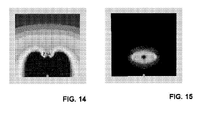
- Figure 12 shows a diagram of the simulated magnetic field strength H of the TEM resonator according to Figure 9 in a tuned state in the y/z-plane.
- the current distribution on the first to third conductor 11, 12, 13 of the above trap circuit can be recognized in this diagram to be nearly even.
- Figure 13 shows the magnetic field strength H in the detuned state, i.e. the diode is non-conducting, in which the butterfly-type current mode is generated.
- Figure 13 shows that this magnetic field strength is significantly smaller and decreases much faster with the distance from the conductors in comparison to the magnetic field strength in the TEM resonant mode indicated in Figure 12 .
- the scale of the magnetic field strength H has a maximum of 100 A/m between the conductor structure and the ground plane (dark area), whereas in Figure 13 this scale has a maximum of only about 5.6 A/m.
- the efficiency of the trap circuit according to the invention has been verified by experiments in which a TEM resonator according to Figure 9 has been constructed for a resonance frequency of about 105 MHz and pick-up coils have been placed close to such a TEM resonator.
- the coupling between the TEM-resonator and the pick-up coil was about -20 dB.
- the original resonance frequency of 105 MHz has been shifted to a lower resonance frequency at about 77 MHz and a higher resonance frequency of about 121 MHz.
- the coupling at the original resonance frequency of 105 MHz was decreased to about -84 dB, i.e. the coupling was reduced by 64dB. Further, no adverse effects of the trap resonance of the trap circuit could be detected.
Landscapes
- Physics & Mathematics (AREA)
- Condensed Matter Physics & Semiconductors (AREA)
- General Physics & Mathematics (AREA)
- Magnetic Resonance Imaging Apparatus (AREA)
Priority Applications (6)
| Application Number | Priority Date | Filing Date | Title |
|---|---|---|---|
| EP10188845A EP2447732A1 (de) | 2010-10-26 | 2010-10-26 | HF-Antennenanordnung mit Entkopplungskreis, insbesondere für ein MRT-System |
| EP11781651.2A EP2633334A1 (de) | 2010-10-26 | 2011-10-25 | Hf-antennenanordnung für mri mit einem sperrkreis |
| CN201180051305XA CN103180748A (zh) | 2010-10-26 | 2011-10-25 | 包括跳陷电路的mri的rf天线装置 |
| JP2013535560A JP2013540553A (ja) | 2010-10-26 | 2011-10-25 | Rfアンテナ及びrf送受信アンテナ装置 |
| PCT/IB2011/054756 WO2012056396A1 (en) | 2010-10-26 | 2011-10-25 | Rf antenna arrangement for mri comprising a trap circuit |
| US13/881,317 US20130207660A1 (en) | 2010-10-26 | 2011-10-25 | Rf antenna arrangement for mri comprising a trap circuit |
Applications Claiming Priority (1)
| Application Number | Priority Date | Filing Date | Title |
|---|---|---|---|
| EP10188845A EP2447732A1 (de) | 2010-10-26 | 2010-10-26 | HF-Antennenanordnung mit Entkopplungskreis, insbesondere für ein MRT-System |
Publications (1)
| Publication Number | Publication Date |
|---|---|
| EP2447732A1 true EP2447732A1 (de) | 2012-05-02 |
Family
ID=43626959
Family Applications (2)
| Application Number | Title | Priority Date | Filing Date |
|---|---|---|---|
| EP10188845A Withdrawn EP2447732A1 (de) | 2010-10-26 | 2010-10-26 | HF-Antennenanordnung mit Entkopplungskreis, insbesondere für ein MRT-System |
| EP11781651.2A Withdrawn EP2633334A1 (de) | 2010-10-26 | 2011-10-25 | Hf-antennenanordnung für mri mit einem sperrkreis |
Family Applications After (1)
| Application Number | Title | Priority Date | Filing Date |
|---|---|---|---|
| EP11781651.2A Withdrawn EP2633334A1 (de) | 2010-10-26 | 2011-10-25 | Hf-antennenanordnung für mri mit einem sperrkreis |
Country Status (5)
| Country | Link |
|---|---|
| US (1) | US20130207660A1 (de) |
| EP (2) | EP2447732A1 (de) |
| JP (1) | JP2013540553A (de) |
| CN (1) | CN103180748A (de) |
| WO (1) | WO2012056396A1 (de) |
Cited By (2)
| Publication number | Priority date | Publication date | Assignee | Title |
|---|---|---|---|---|
| FR3002699A1 (fr) * | 2013-02-27 | 2014-08-29 | Commissariat Energie Atomique | Antenne haute frequence a voies multiples, notamment pour appareil d'imagerie par resonance magnetique nucleaire. |
| CN111157929A (zh) * | 2018-11-08 | 2020-05-15 | 西门子医疗有限公司 | 具有集成的导频音发送器的局部线圈 |
Families Citing this family (6)
| Publication number | Priority date | Publication date | Assignee | Title |
|---|---|---|---|---|
| US9625551B2 (en) * | 2012-04-16 | 2017-04-18 | Ali Caglar Ozen | Magnetic resonance apparatus and data acquisition method with decoupling between transmit and receive coils |
| EP3022571B1 (de) * | 2013-07-18 | 2022-06-22 | Koninklijke Philips N.V. | Auf laminatdesign basierende hochfrequenzspuleneinheit für mrt |
| CN107884732A (zh) * | 2016-09-30 | 2018-04-06 | 西门子(深圳)磁共振有限公司 | 磁共振成像设备、射频线圈及其制造方法 |
| CN107356892B (zh) * | 2017-07-05 | 2019-12-03 | 上海联影医疗科技有限公司 | 一种磁共振射频线圈调节方法、磁共振扫描系统及介质 |
| DE102021000282A1 (de) * | 2020-03-13 | 2021-09-16 | Forschungszentrum Jülich GmbH | Doppeltresonante Spule sowie Array von doppeltresonanten Spulen und deren Verwendung |
| CN112230172B (zh) * | 2020-09-21 | 2023-05-26 | 上海联影医疗科技股份有限公司 | 陷波装置及磁共振系统 |
Citations (6)
| Publication number | Priority date | Publication date | Assignee | Title |
|---|---|---|---|---|
| JPH01129842A (ja) * | 1987-11-16 | 1989-05-23 | Hitachi Medical Corp | 核磁気共鳴イメージング装置 |
| JPH021581A (ja) * | 1987-10-19 | 1990-01-05 | Mitsubishi Electric Corp | Nmr用高周波プローブ及びその調整方法 |
| JPH08322816A (ja) * | 1995-06-05 | 1996-12-10 | Ge Yokogawa Medical Syst Ltd | Mri用rfコイル |
| JPH09276245A (ja) * | 1996-04-18 | 1997-10-28 | Ge Yokogawa Medical Syst Ltd | Mri用rfコイル及びmri装置 |
| US20080297154A1 (en) * | 2007-05-31 | 2008-12-04 | Yosuke Otake | Magnetic field coil and magnetic resonance imaging apparatus |
| US7560931B2 (en) * | 2005-04-22 | 2009-07-14 | Ge Medical Systems Global Technology Company, Llc | Switching device compatible with RF coil and magnetic resonance imaging system |
Family Cites Families (8)
| Publication number | Priority date | Publication date | Assignee | Title |
|---|---|---|---|---|
| US4763076A (en) * | 1987-09-01 | 1988-08-09 | The Regents Of The University Of California | MRI transmit coil disable switching via RF in/out cable |
| WO2007034341A2 (en) * | 2005-09-20 | 2007-03-29 | Koninklijke Philips Electronics N.V. | Rf traps for radio frequency coils used in mri |
| CN1941500B (zh) * | 2005-09-30 | 2011-10-19 | 西门子(中国)有限公司 | 射频发射线圈的去耦合方法 |
| US7932721B2 (en) * | 2006-04-07 | 2011-04-26 | The United States Of America As Represented By The Department Of Health And Human Services | Inductive decoupling of a RF coil array |
| JP5357010B2 (ja) * | 2006-04-24 | 2013-12-04 | コーニンクレッカ フィリップス エヌ ヴェ | コイルシステム及び磁気共鳴システム |
| WO2007138547A2 (en) * | 2006-05-30 | 2007-12-06 | Philips Intellectual Property & Standards Gmbh | Detuning a radio-frequency coil |
| DE102010040260B4 (de) * | 2010-09-03 | 2014-01-09 | Siemens Aktiengesellschaft | Lokalspule mit einer Verstimmeinreichtung |
| US9116214B2 (en) * | 2011-05-31 | 2015-08-25 | General Electric Company | RF coil array having two or more switches built within each RF coil array element, compatible with both magnetic resonance and a temperature mapping |
-
2010
- 2010-10-26 EP EP10188845A patent/EP2447732A1/de not_active Withdrawn
-
2011
- 2011-10-25 WO PCT/IB2011/054756 patent/WO2012056396A1/en active Application Filing
- 2011-10-25 CN CN201180051305XA patent/CN103180748A/zh active Pending
- 2011-10-25 US US13/881,317 patent/US20130207660A1/en not_active Abandoned
- 2011-10-25 JP JP2013535560A patent/JP2013540553A/ja active Pending
- 2011-10-25 EP EP11781651.2A patent/EP2633334A1/de not_active Withdrawn
Patent Citations (6)
| Publication number | Priority date | Publication date | Assignee | Title |
|---|---|---|---|---|
| JPH021581A (ja) * | 1987-10-19 | 1990-01-05 | Mitsubishi Electric Corp | Nmr用高周波プローブ及びその調整方法 |
| JPH01129842A (ja) * | 1987-11-16 | 1989-05-23 | Hitachi Medical Corp | 核磁気共鳴イメージング装置 |
| JPH08322816A (ja) * | 1995-06-05 | 1996-12-10 | Ge Yokogawa Medical Syst Ltd | Mri用rfコイル |
| JPH09276245A (ja) * | 1996-04-18 | 1997-10-28 | Ge Yokogawa Medical Syst Ltd | Mri用rfコイル及びmri装置 |
| US7560931B2 (en) * | 2005-04-22 | 2009-07-14 | Ge Medical Systems Global Technology Company, Llc | Switching device compatible with RF coil and magnetic resonance imaging system |
| US20080297154A1 (en) * | 2007-05-31 | 2008-12-04 | Yosuke Otake | Magnetic field coil and magnetic resonance imaging apparatus |
Non-Patent Citations (1)
| Title |
|---|
| STREIF JÖRG U G ET AL: "A coil combination for magnetic resonance perfusion imaging of mice in vivo at 7 T", REVIEW OF SCIENTIFIC INSTRUMENTS, AIP, MELVILLE, NY, US, vol. 74, no. 5, 1 May 2003 (2003-05-01), pages 2843 - 2848, XP012040846, ISSN: 0034-6748, DOI: 10.1063/1.1568539 * |
Cited By (6)
| Publication number | Priority date | Publication date | Assignee | Title |
|---|---|---|---|---|
| FR3002699A1 (fr) * | 2013-02-27 | 2014-08-29 | Commissariat Energie Atomique | Antenne haute frequence a voies multiples, notamment pour appareil d'imagerie par resonance magnetique nucleaire. |
| EP2772771A1 (de) * | 2013-02-27 | 2014-09-03 | Commissariat A L'energie Atomique Et Aux Energies Alternatives | Hochfrequenzantenne mit Mehrwegesystem, insbesondere für Kernspintomographie |
| US9768498B2 (en) | 2013-02-27 | 2017-09-19 | Commissariat A L'energie Atomique Et Aux Energies Alternatives | High frequency multiple-channel antenna, particularly for a nuclear magnetic resonance imaging device |
| CN111157929A (zh) * | 2018-11-08 | 2020-05-15 | 西门子医疗有限公司 | 具有集成的导频音发送器的局部线圈 |
| US11340322B2 (en) | 2018-11-08 | 2022-05-24 | Siemens Healthcare Gmbh | Local coil with integrated pilot tone transmitter |
| CN111157929B (zh) * | 2018-11-08 | 2022-07-08 | 西门子医疗有限公司 | 具有集成的导频音发送器的局部线圈 |
Also Published As
| Publication number | Publication date |
|---|---|
| JP2013540553A (ja) | 2013-11-07 |
| CN103180748A (zh) | 2013-06-26 |
| US20130207660A1 (en) | 2013-08-15 |
| WO2012056396A1 (en) | 2012-05-03 |
| EP2633334A1 (de) | 2013-09-04 |
Similar Documents
| Publication | Publication Date | Title |
|---|---|---|
| US20130207660A1 (en) | Rf antenna arrangement for mri comprising a trap circuit | |
| US7622928B2 (en) | RF traps for radio frequency coils used in MRI | |
| US7973531B2 (en) | Detuning a radio-frequency coil | |
| US5903150A (en) | Antenna system for NMR and MRI apparatus | |
| US8742759B2 (en) | High-frequency coil and magnetic resonance imaging device | |
| EP2807497B1 (de) | Multiresonante sende-/empfangsantenne zur magnetresonanzbildgebung | |
| US10976388B2 (en) | Minimizing intravascular magnetic resonance imaging (MRI) guidewire heating with single layer MRI transmit/receive radio frequency coil | |
| US8085048B2 (en) | Arrangement to detune a reception antenna in a local coil | |
| US6552544B2 (en) | Detunable coil assembly and method of detuning RF coil for MRI | |
| US10739422B2 (en) | Flexible coaxial magnetic resonance imaging (MRI) coil with integrated decoupling | |
| JP2009534161A (ja) | マルチエレメントrfコイルの簡単なデカップリング並びにそれによるデチューニング及びマッチング機能 | |
| US8237442B2 (en) | Magnetic resonance antenna | |
| CN110168393B (zh) | 低磁场强度下运行的磁共振断层成像设备和局部线圈矩阵 | |
| US11668775B2 (en) | Integrated active detuning for magnetic resonance imaging | |
| US20230261375A1 (en) | Transmission line coupled antenna and detuning circuit | |
| CN110888095B (zh) | 具有失谐电路和能量收集电路的磁共振接收线圈 | |
| EP3652553B1 (de) | Passiver hf-shim-resonator zur homogenisierung einer hf-antennenvorrichtung für tx- und rx-modi | |
| US11169232B2 (en) | Device and method for electrically linking electronic assemblies by means of symmetrical shielded cables | |
| US20210242589A1 (en) | Coil and device for wireless signal transmission, and method for producing such a coil | |
| US8125226B2 (en) | Millipede surface coils | |
| JPH0478294B2 (de) | ||
| RU2172004C2 (ru) | Антенная система для аппаратов магнитно-резонансного изображения и ядерно-магнитно-резонансных аппаратов | |
| Ganti et al. | Achieving electromagnetic compatibility of WPT antennas for medical imaging in MRI | |
| CN212137625U (zh) | 用于局部线圈的对称组件和局部线圈 | |
| JP3836416B2 (ja) | Rf受信コイルおよび磁気共鳴撮像装置 |
Legal Events
| Date | Code | Title | Description |
|---|---|---|---|
| PUAI | Public reference made under article 153(3) epc to a published international application that has entered the european phase |
Free format text: ORIGINAL CODE: 0009012 |
|
| AK | Designated contracting states |
Kind code of ref document: A1 Designated state(s): AL AT BE BG CH CY CZ DE DK EE ES FI FR GB GR HR HU IE IS IT LI LT LU LV MC MK MT NL NO PL PT RO RS SE SI SK SM TR |
|
| AX | Request for extension of the european patent |
Extension state: BA ME |
|
| STAA | Information on the status of an ep patent application or granted ep patent |
Free format text: STATUS: THE APPLICATION IS DEEMED TO BE WITHDRAWN |
|
| 18D | Application deemed to be withdrawn |
Effective date: 20121103 |