EP2445083A1 - Contactless power-feed equipment - Google Patents
Contactless power-feed equipment Download PDFInfo
- Publication number
- EP2445083A1 EP2445083A1 EP10789542A EP10789542A EP2445083A1 EP 2445083 A1 EP2445083 A1 EP 2445083A1 EP 10789542 A EP10789542 A EP 10789542A EP 10789542 A EP10789542 A EP 10789542A EP 2445083 A1 EP2445083 A1 EP 2445083A1
- Authority
- EP
- European Patent Office
- Prior art keywords
- power
- coil
- diode
- primary coil
- center
- Prior art date
- Legal status (The legal status is an assumption and is not a legal conclusion. Google has not performed a legal analysis and makes no representation as to the accuracy of the status listed.)
- Granted
Links
Images


Classifications
-
- H—ELECTRICITY
- H01—ELECTRIC ELEMENTS
- H01F—MAGNETS; INDUCTANCES; TRANSFORMERS; SELECTION OF MATERIALS FOR THEIR MAGNETIC PROPERTIES
- H01F38/00—Adaptations of transformers or inductances for specific applications or functions
- H01F38/14—Inductive couplings
-
- H—ELECTRICITY
- H02—GENERATION; CONVERSION OR DISTRIBUTION OF ELECTRIC POWER
- H02J—ELECTRIC POWER NETWORKS; CIRCUIT ARRANGEMENTS OR SYSTEMS FOR SUPPLYING OR DISTRIBUTING ELECTRIC POWER; SYSTEMS FOR STORING ELECTRIC ENERGY
- H02J50/00—Circuit arrangements or systems for wireless supply or distribution of electric power
- H02J50/005—Mechanical details of housing or structure aiming to accommodate the power transfer means, e.g. mechanical integration of coils, antennas or transducers into emitting or receiving devices
-
- H—ELECTRICITY
- H02—GENERATION; CONVERSION OR DISTRIBUTION OF ELECTRIC POWER
- H02J—ELECTRIC POWER NETWORKS; CIRCUIT ARRANGEMENTS OR SYSTEMS FOR SUPPLYING OR DISTRIBUTING ELECTRIC POWER; SYSTEMS FOR STORING ELECTRIC ENERGY
- H02J50/00—Circuit arrangements or systems for wireless supply or distribution of electric power
- H02J50/10—Circuit arrangements or systems for wireless supply or distribution of electric power using inductive coupling
- H02J50/12—Circuit arrangements or systems for wireless supply or distribution of electric power using inductive coupling of the resonant type
-
- H—ELECTRICITY
- H04—ELECTRIC COMMUNICATION TECHNIQUE
- H04B—TRANSMISSION
- H04B5/00—Near-field transmission systems, e.g. inductive or capacitive transmission systems
- H04B5/70—Near-field transmission systems, e.g. inductive or capacitive transmission systems specially adapted for specific purposes
- H04B5/79—Near-field transmission systems, e.g. inductive or capacitive transmission systems specially adapted for specific purposes for data transfer in combination with power transfer
-
- H—ELECTRICITY
- H02—GENERATION; CONVERSION OR DISTRIBUTION OF ELECTRIC POWER
- H02M—APPARATUS FOR CONVERSION BETWEEN AC AND AC, BETWEEN AC AND DC, OR BETWEEN DC AND DC, AND FOR USE WITH MAINS OR SIMILAR POWER SUPPLY SYSTEMS; CONVERSION OF DC OR AC INPUT POWER INTO SURGE OUTPUT POWER; CONTROL OR REGULATION THEREOF
- H02M3/00—Conversion of DC power input into DC power output
- H02M3/22—Conversion of DC power input into DC power output with intermediate conversion into AC
- H02M3/24—Conversion of DC power input into DC power output with intermediate conversion into AC by static converters
- H02M3/28—Conversion of DC power input into DC power output with intermediate conversion into AC by static converters using discharge tubes with control electrode or semiconductor devices with control electrode to produce the intermediate AC
- H02M3/325—Conversion of DC power input into DC power output with intermediate conversion into AC by static converters using discharge tubes with control electrode or semiconductor devices with control electrode to produce the intermediate AC using devices of a triode or a transistor type requiring continuous application of a control signal
- H02M3/335—Conversion of DC power input into DC power output with intermediate conversion into AC by static converters using discharge tubes with control electrode or semiconductor devices with control electrode to produce the intermediate AC using devices of a triode or a transistor type requiring continuous application of a control signal using semiconductor devices only
- H02M3/337—Conversion of DC power input into DC power output with intermediate conversion into AC by static converters using discharge tubes with control electrode or semiconductor devices with control electrode to produce the intermediate AC using devices of a triode or a transistor type requiring continuous application of a control signal using semiconductor devices only in push-pull configuration
- H02M3/3372—Conversion of DC power input into DC power output with intermediate conversion into AC by static converters using discharge tubes with control electrode or semiconductor devices with control electrode to produce the intermediate AC using devices of a triode or a transistor type requiring continuous application of a control signal using semiconductor devices only in push-pull configuration of the parallel type
-
- Y—GENERAL TAGGING OF NEW TECHNOLOGICAL DEVELOPMENTS; GENERAL TAGGING OF CROSS-SECTIONAL TECHNOLOGIES SPANNING OVER SEVERAL SECTIONS OF THE IPC; TECHNICAL SUBJECTS COVERED BY FORMER USPC CROSS-REFERENCE ART COLLECTIONS [XRACs] AND DIGESTS
- Y02—TECHNOLOGIES OR APPLICATIONS FOR MITIGATION OR ADAPTATION AGAINST CLIMATE CHANGE
- Y02B—CLIMATE CHANGE MITIGATION TECHNOLOGIES RELATED TO BUILDINGS, e.g. HOUSING, HOUSE APPLIANCES OR RELATED END-USER APPLICATIONS
- Y02B70/00—Technologies for an efficient end-user side electric power management and consumption
- Y02B70/10—Technologies improving the efficiency by using switched-mode power supplies [SMPS], i.e. efficient power electronics conversion e.g. power factor correction or reduction of losses in power supplies or efficient standby modes
Definitions
- the present invention relates to contactless power-feed equipment and particularly relates to a power-supply device that supplies an AC current to an induction line or an induction coil.
- Patent Literature 1 discloses an example of a conventional power-supply device that supplies an AC current to the induction line.
- the power-supply device includes: a DC choke fed with a DC current from the positive output terminal of a DC power supply; a high-frequency transformer including a primary coil having a center tap fed with a DC current through the DC choke and a secondary coil connected to the induction line; a capacitor connected in parallel with both ends of the primary coil of the high-frequency transformer; a first switch connected between one end of the primary coil of the high-frequency transformer and the negative output terminal of the DC power supply; and a second switch connected between the other end of the primary coil of the high-frequency transformer and the negative output terminal of the DC power supply.
- the primary coil and the secondary coil of the high-frequency transformer, the induction line, and the capacitor are selected so as to form a resonance circuit resonating at a predetermined frequency.
- the first switch and the second switch are alternately switched by a switching controller every 180° such that a current passes through the secondary coil at the predetermined frequency.
- the number of windings on the secondary side of the high-frequency transformer is set at one to increase a current passing through the induction line and minimize the influence of a change of load.
- the high-frequency transformer provides insulation from the DC power supply and supplies a large current of a sinusoidal waveform at the predetermined frequency to the induction line.
- the first switch and the second switch should be switched at phases shifted by exactly 180°.
- a capacitor connected in series with the switches forms a loop circuit that discharges electricity, resulting in excessive energy consumption.
- a noise current generated by the switching passes through the capacitor and leads to excessive energy consumption.
- a switching controller is required to switch the first and second switches.
- An object of the present invention is to provide contactless power-feed equipment that can prevent excessive energy consumption upon switching and eliminate the need for a switching controller.
- a first aspect of the present invention is contactless power-feed equipment including an induction line placed along a travel path of a movable body and fed with an AC current, or an induction coil that is disposed at a predetermined position for holding a device and fed with an AC current, the movable body including a power-receiving coil on which an electromotive force is induced by a magnetic flux generated on the induction line, or the device including a power-receiving coil on which an electromotive force is induced by a magnetic flux generated on the induction coil
- the contactless power-feed equipment including: a DC power-supply device that supplies a DC current; a DC choke having one end connected to the positive output terminal of the DC power-supply device; an insulating transformer including a center-tapped primary coil having a center tap connected to the other end of the DC choke and a secondary coil connected to one of the induction line and the induction coil; a resonance capacitor that is connected in parallel with the secondary coil and forms a
- the DC current is supplied from the DC power-supply device to the center-tapped primary coil through the DC choke to drive the first switching element.
- the DC current passes through the first diode and the first switching element from the one end of the center-tapped primary coil.
- the second switching element is driven to pass the DC current from the other end of the center-tapped primary coil through the second diode and the second switching element.
- the first switching element and the second switching element are alternately driven so as to alternately pass a current from the one end and the other end of the center-tapped primary coil, leading to an alternately reversed current passing through the secondary coil.
- the first switching element and the second switching element are alternately driven so as to pass the AC current through the secondary coil at the predetermined frequency.
- the AC current passes through one of the induction line and the induction coil from the secondary coil at the predetermined frequency.
- a loop circuit including the switching elements is not fed with a circulating current in response to the operations of the switching elements, reducing an energy loss.
- a capacitor connected to the switching elements is absent and the first and second diodes are provided.
- the recovery current of the diodes causes an instant current flow at the application of a reverse voltage. Since only the primary coil is connected, it is possible to prevent the circulating current from passing through the loop circuit, reducing an energy loss.
- a second aspect of the present invention is the first aspect of the present invention, in which the first switching element and the second switching element each include a transistor, the contactless power-feed equipment includes: a first Zener diode having a cathode connected to the one end of the center-tapped primary coil and the base of the transistor forming the second switching element and an anode connected to the negative output terminal of the DC power-supply device; and a second Zener diode having a cathode connected to the other end of the center-tapped primary coil and the base of the transistor forming the first switching element and an anode connected to the negative output terminal of the DC power-supply device, a current passing through the first Zener diode from the one end of the center-tapped primary coil drives the transistor forming the second switching element, and a current passing through the second Zener diode from the other end of the center-tapped primary coil drives the transistor forming the first switching element.
- the Zener voltage of the first Zener diode is applied to the base of the second transistor to drive the second transistor.
- a current passes through the second diode having the cathode connected to the second transistor, so that a current flow to the primary coil is reversed.
- the base voltage of the second transistor becomes 0, the Zener voltage of the second Zener diode is applied to the base of the first transistor to drive the first transistor, and a current passes through the first diode having the cathode connected to the first transistor, so that a current flow to the primary coil is reversed.
- the first transistor and the second transistor are alternately turned on.
- the direction of the current flow to the primary coil is reversed each time the transistors are switched. Accordingly, a current passing through the secondary coil is alternately reversed.
- the current flow is maximized at the predetermined frequency that allows a circuit including the resonance capacitor and one of the induction line and the induction coil to form a resonance circuit, so that the first transistor and the second transistor are driven at the predetermined frequency of the circuit.
- the AC current is supplied by self-oscillation to one of the induction line and the induction coil at the predetermined frequency of the circuit.
- a switching controller for driving the transistors (switching elements) is not necessary.
- a third aspect of the present invention is the first or second aspect of the present invention, in which the AC current passing through one of the induction line and the induction coil has a frequency that falls below the predetermined frequency in the presence of one of the movable body and the power-receiving coil of the device.
- the resonance capacitor and one of the induction line and the induction coil form the resonance circuit at the predetermined frequency-
- the impedance of the circuit increases in the presence of one of the movable body and the power-receiving coil of the device, so that a resonance frequency decreases and a self-oscillation frequency falls below the predetermined frequency, accordingly.
- a fourth aspect of the present invention is the third aspect of the present invention, in which a load connected to the power-receiving coil has a rating that is set based on the reduced frequency.
- the load fed with power from one of the movable body and the power-receiving coil of the device has a predetermined rating that enables driving at the reduced frequency.
- a fifth aspect of the present invention is any one of the first to fourth aspects of the present invention, in which the induction coil and the power-receiving coil are each wound around both legs of cores formed in channel shape in side view, and a voltage induced on the power-receiving coil is limited to a predetermined voltage or lower because of the saturation of the cores.
- the voltage of the power-receiving coil is not higher than the predetermined voltage because of the saturation of the cores.
- the received power of the power-receiving coil is limited, preventing an overload on the induction coil.
- a sixth aspect of the present invention is the fifth aspect of the present invention, in which the core of the power-receiving coil is smaller than the core of the induction coil.
- the core of the power-receiving coil is smaller than the core of the induction coil.
- a seventh aspect of the present invention is contactless power-feed equipment including an induction line placed along a travel path of a movable body and fed with an AC current, or an induction coil that is disposed at a predetermined position for holding a device and fed with an AC current, the movable body including a power-receiving coil on which an electromotive force is induced by a magnetic flux generated on the induction line, or the device including a power-receiving coil on which an electromotive force is induced by a magnetic flux generated on the induction coil
- the contactless power-feed equipment including: a DC power-supply device that supplies a DC current; a DC choke having one end connected to the positive output terminal of the DC power-supply device; an insulating transformer including a center-tapped primary coil having a center tap connected to the other end of the DC choke and a secondary coil connected to one of the induction line and the induction coil; a resonance capacitor that is connected in parallel with the secondary coil and forms a resonance circuit with one of the
- the DC current supplied to the center-tapped primary coil from the DC power-supply device through the DC choke is supplied to the first Zener diode through the first constant current diode or to the second Zener diode through the second constant current diode, the Zener voltage of the first Zener diode or the second Zener diode is applied to the base of the transistor forming the first switching element or the base of the transistor forming the second switching element, and one of the first switching element and the second switching element is turned on when the Zener voltage reaches a predetermined base voltage with a small time delay, so that the circuit is raised.
- the first switching element is driven, the charge of the base of the second switching element is discharged through the first switching diode.
- the second switching element is driven, the charge of the base of the first switching element is discharged by the second switching diode.
- the constant current diode is used to raise the Zener voltage for supplying the base voltage of the transistor forming the switching element, so that the Zener voltage is stably raised without causing a time delay and a more stable switching operation is achieved.
- a loop circuit including the switching elements is not fed with a circulating current in response to the operations of the switching elements, reducing an energy loss.
- a capacitor connected to the switching elements is absent and first and second diodes are provided.
- the recovery current of the diodes causes an instant current flow at the application of a reverse voltage. Since only the primary coil is connected, it is possible to prevent the circulating current from passing through the loop circuit, reducing an energy loss.
- a constant current diode is used to raise a Zener voltage for supplying the base voltage of the transistor forming the switching element, so that the Zener voltage is stably raised without causing a time delay and a more stable switching operation is achieved.
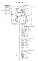
- FIG. 1 is a circuit diagram illustrating contactless power-feed equipment according to a first embodiment of the present invention.
- a primary side includes a DC power-supply device 11, a power-feed device 12, and a power-feed unit 13 and a secondary side (power-receiving side) includes a power-receiving unit 15.
- the power-feed unit 13 is disposed at a predetermined position where a moving device (not shown) including the power-receiving unit 15 is held.
- a chain line indicates a travel path 17 of the device.
- the DC power-supply device 11 receives power from a commercial AC power supply, converts an AC current to a DC current, and supplies the DC current of a rated DC voltage to the power-feed device 12.
- the power-feed device 12 includes:
- the cathode of the first Zener diode 29 is connected to the one end 22b of the center-tapped primary coil 22 via the first resistor 28.
- the anode of the first Zener diode 29 is connected to the negative output terminal of the DC power-supply device 11.
- the cathode of the second Zener diode 32 is connected to the other end 22c of the center-tapped primary coil 22 via the second resistor 31.
- the anode of the second Zener diode 32 is connected to the negative output terminal of the DC power-supply device 11.
- a current passing through the first Zener diode 29 from the one end 22b of the center-tapped primary coil 22 drives the second transistor 36 and a current passing through the second Zener diode 32 from the other end 22c of the center-tapped primary coil 22 drives the first transistor 35.
- the power-feed unit 13 has flat ferrite core members 41 combined in channel shape in side view.
- the ferrite core members 41 are horizontally combined with the ends of legs 13A.
- the channel-shaped legs 13A are each wound with an induction coil 42 to form a power-feed member 43.
- the two power-feed members 43 are disposed on an aluminum floor part 44 such that channel-shaped spaces are arranged in series in moving direction X of the power-receiving unit 15.
- the power-receiving unit 15 includes a power-receiving member 52 ( FIG. 2 ) wound with power-receiving coils 51, a resonance capacitor 53 that forms a resonance circuit at a resonance frequency, which will be described later, with the power-receiving coils 51, and a rectifier 54 that is connected in parallel with the resonance capacitor 53.
- the power-receiving member 52 has flat ferrite core members 56 combined in channel shape in side view.
- the ferrite core members 56 are horizontally combined with the ends of channel-shaped legs 52A.
- the channel-shaped legs 52A are wound with the power-receiving coils 51 and are fixed on an aluminum floor part 57.
- a voltage generated in the power-receiving member 52 is limited to a predetermined voltage or lower because of the saturation voltages of the ferrite core members 56. As shown in FIGS.
- the ferrite core members 56 of the power-receiving member 52 are smaller in size than the ferrite core members 41 of the power-feed unit 13 (induction coils 42) and the shape (dimensions) of the power-receiving member 52 is smaller than the shape (dimensions) of the power-feed member 43.
- the power-receiving member 52 (power-receiving coils 51) is moved such that the ferrite core members 56 disposed on the ends of the legs 52A of the power-receiving member 52 are opposed to the ferrite core members 41 disposed on the ends of the four legs 13A of the power-feed unit 13.
- the DC current supplied to the DC choke 21 varies in flowability depending on, for example, the forward voltages of the diodes 26 and 27, variations in the characteristics of the transistors 35 and 36, and the resistance errors of the resistors 28, 30, 31, and 33 even if the ratings of components are the same. In this case, it is assumed that a current passes through the second Zener diode 32 from the other end 22c of the center-tapped primary coil 22, the first transistor 35 has a base voltage of 0.7 V, and then the first transistor 35 is first turned on (conducting).
- the DC current supplied to the DC choke 21 passes through the one end 22b, the first diode 26, and the first transistor 35 from the center tap 22a of the primary coil 22 and then flows to the first Zener diode 29 from the one end 22b through the first resistor 28.
- the charge of the gate of the first transistor 35 flows to the other end 22c of the center-tapped primary coil 22 through the second gate resistor 33 and the second resistor 31, the first transistor 35 has a gate voltage of 0 v, and the first transistor 35 is turned off (non-conducting). At the same time, the second transistor 36 having a base voltage of 0.7 V is turned on (conducting).
- the DC current supplied to the DC choke 21 passes through the other end 22c, the second diode 27, and the second transistor 36 from the center tap 22a of the primary coil 22 and then flows to the second Zener diode 32 from the other end 22c through the second resistor 31.
- the charge of the gate of the second transistor 36 flows to the one end 22b of the center-tapped primary coil 22 through the first gate resistor 30 and the first resistor 28, the second transistor 36 has a gate voltage of 0 V, and the second transistor 36 is turned off (non-conducting). At the same time, the first transistor 35 having a base voltage of 0.7 v is turned on (conducting).
- the first transistor 35 and the second transistor 36 are alternately turned on.
- the direction of a current flow to the primary coil 22 is reversed each time the transistors are switched.
- a current passing through the secondary coil 23 is alternately reversed.
- the current flow is maximized at the resonance frequency (e.g., 15 kHz) of a circuit including the resonance capacitor 25 and the induction coils 42 of the power-feed unit 13, so that the first transistor 35 and the second transistor 36 are alternately switched at the resonance frequency every 180°.
- self-oscillation is obtained at the resonance frequency of the circuit including the resonance capacitor 25 and the induction coils 42 of the power-feed unit 13, and the AC current of the resonance frequency is supplied to the induction coils 42.
- a control circuit for driving the first transistor 35 and the second transistor 36 is not necessary.
- the frequency of the AC current passing through the induction coils 42 falls below (e.g., to 14 kHz) the predetermined frequency (the resonance frequency of the circuit including the resonance capacitor 25 and the induction coils 42) and a self-oscillation frequency decreases, accordingly.
- the power-receiving coils 51 and the resonance capacitor 53 of the power-receiving unit 15 are selected such that the reduced frequency (e.g., 14 kHz) serves as a resonance frequency.
- a voltage generated on the power-receiving member 52 (power-receiving coils 51) is limited to the predetermined voltage or lower because of the saturation voltages of the ferrite core members 56, thereby limiting the received power of the power-receiving unit 15.
- a loop circuit including the transistors 35 and 36 is not fed with a circulating current in response to the operations of the transistors 35 and 36 or is not fed with a noise current generated upon the switching of the transistors 35 and 36, reducing an energy loss.
- a capacitor connected to the transistors 35 and 36 is absent and the first and second diodes 26 and 27 are provided.
- the recovery current of the diodes 26 and 27 causes a current flow at the application of a reverse voltage. Since only the primary coil 22 is connected, it is possible to prevent the circulating current from passing through the loop circuit, achieving a smaller energy loss and higher efficiency.
- the self-oscillation of the transistors 35 and 36 can eliminate the need for a control circuit for driving the transistors 35 and 36.
- a current passes through the induction coils 42 at a higher frequency than in the presence of the power-receiving unit 15.
- a small current is required, reducing an energy loss in the absence of the power-receiving unit 15.
- the ferrite core member 56 of the power-receiving coil 51 is smaller in size than the ferrite core member 41 of the induction coil 42. Thus, even if the position of the ferrite core member 56 of the power-receiving coil 51 is displaced from the position of the ferrite core member 41 of the induction coil 42, a voltage required for the power-receiving coil 51 can be induced.
- a voltage generated on the power-receiving member 52 is limited to the predetermined voltage or lower because of the saturated voltages of the ferrite core members 56.
- the received power of the power-receiving unit 15 is limited, preventing an overload on the induction coil 42 (primary side).
- FIG. 4 is a circuit diagram illustrating contactless power-feed equipment according to a second embodiment of the present invention.
- the same circuit configurations as in the first embodiment are indicated by the same reference numerals and the explanation thereof is omitted.
- the power-feed unit 13 is connected to the resonance capacitor 25, whereas in the second embodiment, as shown in FIG. 4 , an induction line 62 forming a resonance circuit with a resonance capacitor 25 at a predetermined frequency is connected instead of the power-feed unit 13.
- the induction line 62 is laid along a travel path 61 of movable bodies.
- Power-receiving units 15 are mounted on the movable bodies and receive power from the induction line 62.
- the impedance of a circuit connected to the resonance capacitor 25 of a power-feed device 12 fluctuates with the power of a load connected to the power-receiving unit 15, changing a resonance frequency.
- an electromotive force fluctuates that is induced to the power-receiving unit 15.
- the movable bodies need to be rated so as to feed power to the load even if the fluctuation of the electromotive force varies with a frequency fluctuation.
- FIG. 5 is a circuit diagram illustrating contactless power-feed equipment according to a third embodiment of the present invention.
- the same circuit configurations as in the first embodiment are indicated by the same reference numerals and the explanation thereof is omitted.
- the gate charges of the transistors 35 and 36 to be placed into a non-conducting state are released through the resistors 31, 33, 28, and 30 to reduce the gate voltages.
- the gate voltages may be slowly reduced and thus the transistors 35 and 36 may be slowly switched, precluding the acquisition of a secondary current at a desired high frequency (e.g., 15 kHz).
- the contactless power-feed equipment further includes: a discharge bypass circuit that quickly attenuates the gate charges of transistors 35 and 36 to quickly reduce the gate voltage to 0 V (discharging); and a gate quick-charge circuit that quickly charges the gates of the transistors 35 and 36 to rapidly increase the gate voltages, so that the transistors 35 and 36 can be quickly switched and a secondary current is obtained at a desired high frequency even if a large current is applied.
- the discharge bypass circuit includes:
- the addition of the discharge bypass circuit makes it possible to quickly discharge the gate voltages of the transistors 35 and 36 to be placed into a non-conducting state.
- the addition of the gate quick-charge circuit makes it possible to quickly raise the gate voltages of the transistors 35 and 36 to be placed into a conducting state.
- the transistors 35 and 36 can be quickly switched to obtain a secondary current at a desired high frequency.
- a power-feed unit 13 is connected to a power-feed device 12.
- An induction line 62 may be connected instead.
- FIG. 6 is a circuit diagram illustrating contactless power-feed equipment according to a fourth embodiment of the present invention.
- the same circuit configurations as in the first embodiment are indicated by the same reference numerals and the explanation thereof is omitted.
- the first diode 26 is removed and the collector of a first (NPN) transistor (an example of a first switching element) 35 is connected to one end 22b of a center-tapped primary coil 22.
- NPN first (NPN) transistor
- the second diode 27 is removed and the collector of a second (NPN) transistor (an example of the first switching element) 36 is connected to another end 22c of the center-tapped primary coil 22.
- NPN second
- a first constant current diode 39 and a first switching diode 37 are provided instead of the first resistor 28.
- the first constant current diode 39 has an anode connected to the one end 22b of the center-tapped primary coil 22 and a cathode connected to the cathode of a first Zener diode 29.
- the first switching diode 37 has an anode connected to the cathode of the first constant current diode 39 and a cathode connected to the one end 22b of the center-tapped primary coil 22.
- a second constant current diode 40 and a second switching diode 38 are provided instead of the second resistor 31.
- the second constant current diode 40 has an anode connected to the other end 22c of the center-tapped primary coil 22 and a cathode connected to the cathode of a second Zener diode 32.
- the second switching diode 38 has an anode connected to the cathode of the second constant current diode 40 and a cathode connected to the other end 22c of the center-tapped primary coil 22.
- a resonance capacitor 25 is provided outside a power-feed device 12 and is connected in parallel with the power-feed device 12.
- an induction line 62 is connected that forms a resonance circuit with the resonance capacitor 25 at a predetermined frequency.
- the DC current supplied to the DC choke 21 varies in flowability depending on, for example, the forward voltages of the constant current diodes 39 and 40 and variations in the characteristics of the transistors 35 and 36 even if the ratings of components are the same.
- a current flows to the second Zener diode 32 from the other end 22c of the center-tapped primary coil 22 through the second constant current diode 40, the base voltage of the first transistor 35 is at least a threshold voltage, and the first transistor 35 is first turned on (conducting).
- the first transistor 35 When the first transistor 35 is first turned on (conducting), the DC current supplied to the DC choke 21 passes through the one end 22b and the first transistor 35 from a center tap 22a of the primary coil 22. At this point, the voltage of the one end 22b of the primary coil 22 is substantially 0 V and thus the charge of the base of the second transistor 36 is discharged to the one end 22b of the primary coil 22 through the first switching diode 37, so that the second transistor 36 is completely turned off (non-conducting).
- the current passing through the first transistor 35 from the primary coil 22 is supplied to the resonance capacitor 25 and the induction line 62 forming a resonance circuit with the resonance capacitor 25, through a secondary coil 23.
- the induction line 62 and the resonance capacitor 25 starts resonating at the predetermined frequency and a voltage across the secondary coil 23 is reversed after a certain period of time. Accordingly, the voltage of the other end 22c of the primary coil 22 falls below the voltage of the one end 22b.
- the charge of the base of the first transistor 35 is discharged to the other end 22c of the primary coil 22 through the second switching diode 38.
- the first transistor 35 is turned off (non-conducting).
- the first transistor 35 and the second transistor 36 are alternately turned on.
- the direction of a current flow to the primary coil 22 is reversed each time the transistors are switched. 8.
- a current passing through the secondary coil 23 is alternately reversed.
- the current flow is maximized at the resonance frequency (e.g., 15 kHz) of a circuit including the resonance capacitor 25 and the induction line 62, so that the first transistor 35 and the second transistor 36 are alternately switched at the resonance frequency every 180°.
- self-oscillation is obtained at the resonance frequency of the circuit including the resonance capacitor 25 and the induction line 62, and the AC current of the resonance frequency is supplied to the induction line 62.
- a control circuit for driving the first transistor 35 and the second transistor 36 is not necessary.
- Magnetic fluxes generated on the induction line 62 cause a large electromotive force on a power-receiving unit 15 mounted on a movable body.
- An AC current generated by the electromotive force is supplied to a rectifier 54 and then a DC current rectified by the rectifier 54 is supplied to the load of the movable body.
- power-receiving coils 51 of the movable body increase the impedance of a circuit connected to the resonance capacitor 25 of the power-feed device 12.
- the frequency of the AC current passing through the induction line 62 falls below (e.g., to 14 kHz) the predetermined frequency (the resonance frequency of the circuit including the resonance capacitor 25 and the induction line 62) and a self-oscillation frequency decreases, accordingly.
- the power-receiving coils 51 and a resonance capacitor 53 of the power-receiving unit 15 are selected such that the reduced frequency (e.g., 14 kHz) serves as a resonance frequency.
- a voltage generated on a power-receiving member 52 is limited to the predetermined voltage or lower because of the saturation voltages of ferrite core members 56, thereby limiting the received power of the power-receiving unit 15.
- a loop circuit including the transistors 35 and 36 is not fed with a circulating current in response to the operations of the transistors 35 and 36 and the loop circuit is not fed with a noise current generated upon the switching of the transistors 35 and 36.
- a capacitor connected to the transistors 35 and 36 is not provided.
- the first constant current diode 39 is provided instead of the first resistor 28 and the second constant current diode 40 is provided instead of the second resistor 31.
- the Zener voltage can be stably raised without causing a time delay, achieving a more stable switching operation.
- the induction path 62 is connected to the power-feed device 12.
- the power-feed unit 13 may be connected instead.
- FIG. 7 is a circuit diagram showing contactless power-feed equipment according to a fifth embodiment of the present invention.
- the same circuit configurations as in the fourth embodiment are indicated by the same reference numerals and the explanation thereof is omitted.
- two power-feed devices 12 of the fourth embodiment are connected to induction lines 62.
- a plurality of capacitors 72 are connected in parallel at predetermined intervals between the pair of the induction lines 62.
- the ends of the adjacent capacitors 72 are connected to each other via a zero-impedance cable 73-
- the starting end of an induction line 71 configured thus is connected to the power-feed device 12 (one of the power-feed device 12) of the fourth embodiment and the terminal end of the induction line 71 is connected to the power-feed device 12 (the other power-feed device 12) of the fourth embodiment.
- the two power-feed devices 12 supply an induced current to the induction lines 62.
- the two power-feed devices 12 self-oscillate with the frequency and phase of the same induced current, so that the power-feed devices 12 can supply induced currents in synchronization with each other without cancelling the induced currents, thereby substantially doubling the power source capacity of the overall circuit.
- the number of movable bodies (power-receiving units 15) receiving power from the induction lines 62 increases, power can be supplied with sufficient stability.
- a storage device e.g., a battery or an electric double-layer capacitor
- the storage device 75 can be charged by an induced current supplied to a secondary coil 23 of an insulating transformer 24 connected to the induction lines 62.
- the storage device 75 is charged by forming a closed loop in which a current passing through the secondary coil 23 causes a current to flow to a center-tapped primary coil 22, the current at this point passes through a DC choke 21, the storage device 75, and a diode across a second transistor 36, and a current in opposite phase passes through the DC choke 21, the storage device 75, and a diode across the first transistor 35.
- the diodes 26 and 27 are not provided between the one end 22b of the center-tapped primary coil 22 and the collector of the first transistor 35 and between the other end 22c of the center-tapped primary coil 22 and the collector of the second transistor 36 unlike in the power-feed device 12 of the first embodiment, so that the closed loop is formed.
- the storage device 75 can be charged beforehand by the other power-feed device 12 connected to the DC power-supply device 11.
- a current can be supplied to the induction lines 62 by the two power-feed devices 12.
- the DC power-supply devices 11 are connected to the respective power-feed devices 12, so that even if a failure occurs on one of the DC power-supply devices 11, discharging from the storage device 75 enables stable current supply to the induction lines 62.
- the power-feed devices 12 of the fourth embodiment are connected to the induction lines 62, the power-feed devices 12 are synchronized with each other with the same frequency and phase in the circuit without cancelling the generated induced currents.
- the power source capacity of the overall circuit can be substantially doubled without using any additional measures.
- the diverse operations can be performed and power can be stably supplied to the induction lines 62.
- one of the power-feed devices 12 is connected to the starting end of the induction line 71 and the other power-feed device 12 is connected to the terminal end of the induction line 71.
- the connected point of the other power-feed device 12 is not limited to the terminal end of the induction line 71 and thus it is obvious that the other power-feed device 12 can be connected to some midpoint of the induction line 71.
- the connected point of the power-feed device 12 is more flexibly determined, that is, flexibility in choosing the location of the power-feed device 12 increases, so that the equipment can have higher flexibility.
- the two power-feed devices 12 are connected to the induction lines 62.
- the number of power-feed devices 12 is not limited to two and thus more power-feed devices 12 can be connected.
- the transistors 35 and 36 are used as switching elements. Simple switches may be used instead.
- a switching controller is necessary for alternately switching a first switching element and a second switching element such that an AC current passes through the secondary coil 23 at the predetermined frequency.
Landscapes
- Engineering & Computer Science (AREA)
- Power Engineering (AREA)
- Computer Networks & Wireless Communication (AREA)
- Signal Processing (AREA)
- Dc-Dc Converters (AREA)
- Current-Collector Devices For Electrically Propelled Vehicles (AREA)
- Charge And Discharge Circuits For Batteries Or The Like (AREA)
Abstract
Description
- The present invention relates to contactless power-feed equipment and particularly relates to a power-supply device that supplies an AC current to an induction line or an induction coil.
-
Patent Literature 1 discloses an example of a conventional power-supply device that supplies an AC current to the induction line. - The power-supply device includes: a DC choke fed with a DC current from the positive output terminal of a DC power supply; a high-frequency transformer including a primary coil having a center tap fed with a DC current through the DC choke and a secondary coil connected to the induction line; a capacitor connected in parallel with both ends of the primary coil of the high-frequency transformer; a first switch connected between one end of the primary coil of the high-frequency transformer and the negative output terminal of the DC power supply; and a second switch connected between the other end of the primary coil of the high-frequency transformer and the negative output terminal of the DC power supply.
- The primary coil and the secondary coil of the high-frequency transformer, the induction line, and the capacitor are selected so as to form a resonance circuit resonating at a predetermined frequency. The first switch and the second switch are alternately switched by a switching controller every 180° such that a current passes through the secondary coil at the predetermined frequency. The number of windings on the secondary side of the high-frequency transformer is set at one to increase a current passing through the induction line and minimize the influence of a change of load.
- Thus, the high-frequency transformer provides insulation from the DC power supply and supplies a large current of a sinusoidal waveform at the predetermined frequency to the induction line.
-
- Patent Literature 1: Japanese Patent No.
2667054 FIG. 6 ) - In conventional contactless power-feed equipment, the first switch and the second switch should be switched at phases shifted by exactly 180°. However, if the switching timing is shifted so that both switches are turned on simultaneously, a capacitor connected in series with the switches forms a loop circuit that discharges electricity, resulting in excessive energy consumption. Moreover, a noise current generated by the switching passes through the capacitor and leads to excessive energy consumption. Furthermore, a switching controller is required to switch the first and second switches.
- An object of the present invention is to provide contactless power-feed equipment that can prevent excessive energy consumption upon switching and eliminate the need for a switching controller.
- In order to attain the object, a first aspect of the present invention is contactless power-feed equipment including an induction line placed along a travel path of a movable body and fed with an AC current, or an induction coil that is disposed at a predetermined position for holding a device and fed with an AC current, the movable body including a power-receiving coil on which an electromotive force is induced by a magnetic flux generated on the induction line, or the device including a power-receiving coil on which an electromotive force is induced by a magnetic flux generated on the induction coil,
the contactless power-feed equipment including: a DC power-supply device that supplies a DC current; a DC choke having one end connected to the positive output terminal of the DC power-supply device; an insulating transformer including a center-tapped primary coil having a center tap connected to the other end of the DC choke and a secondary coil connected to one of the induction line and the induction coil; a resonance capacitor that is connected in parallel with the secondary coil and forms a resonance circuit with one of the induction line and the induction coil at a predetermined frequency; a first diode having an anode connected to one end of the center-tapped primary coil; a second diode having an anode connected to the other end of the center-tapped primary coil; a first switching element connected between the cathode of the first diode and the negative output terminal of the DC power-supply device; and a second switching element connected between the cathode of the second diode and the negative output terminal of the DC power-supply device, wherein the first switching element and the second switching element are alternately driven so as to pass the AC current through the secondary coil at the predetermined frequency. - With this configuration, the DC current is supplied from the DC power-supply device to the center-tapped primary coil through the DC choke to drive the first switching element. At this point, the DC current passes through the first diode and the first switching element from the one end of the center-tapped primary coil. Then, the second switching element is driven to pass the DC current from the other end of the center-tapped primary coil through the second diode and the second switching element. The first switching element and the second switching element are alternately driven so as to alternately pass a current from the one end and the other end of the center-tapped primary coil, leading to an alternately reversed current passing through the secondary coil. At this point, the first switching element and the second switching element are alternately driven so as to pass the AC current through the secondary coil at the predetermined frequency. Thus, the AC current passes through one of the induction line and the induction coil from the secondary coil at the predetermined frequency.
- Moreover, even if the switching timing of the switching elements is shifted so that the elements are simultaneously turned on, a loop circuit including the switching elements is not fed with a circulating current in response to the operations of the switching elements, reducing an energy loss. This is because a capacitor connected to the switching elements is absent and the first and second diodes are provided. Furthermore, the recovery current of the diodes causes an instant current flow at the application of a reverse voltage. Since only the primary coil is connected, it is possible to prevent the circulating current from passing through the loop circuit, reducing an energy loss.
- A second aspect of the present invention is the first aspect of the present invention, in which the first switching element and the second switching element each include a transistor, the contactless power-feed equipment includes: a first Zener diode having a cathode connected to the one end of the center-tapped primary coil and the base of the transistor forming the second switching element and an anode connected to the negative output terminal of the DC power-supply device; and a second Zener diode having a cathode connected to the other end of the center-tapped primary coil and the base of the transistor forming the first switching element and an anode connected to the negative output terminal of the DC power-supply device, a current passing through the first Zener diode from the one end of the center-tapped primary coil drives the transistor forming the second switching element, and a current passing through the second Zener diode from the other end of the center-tapped primary coil drives the transistor forming the first switching element.
- With this configuration, when the current passes through the first Zener diode from the one end of the center-tapped primary coil, the Zener voltage of the first Zener diode is applied to the base of the second transistor to drive the second transistor. A current passes through the second diode having the cathode connected to the second transistor, so that a current flow to the primary coil is reversed. Then, the base voltage of the second transistor becomes 0, the Zener voltage of the second Zener diode is applied to the base of the first transistor to drive the first transistor, and a current passes through the first diode having the cathode connected to the first transistor, so that a current flow to the primary coil is reversed. In this way, the first transistor and the second transistor are alternately turned on. The direction of the current flow to the primary coil is reversed each time the transistors are switched. Accordingly, a current passing through the secondary coil is alternately reversed. The current flow is maximized at the predetermined frequency that allows a circuit including the resonance capacitor and one of the induction line and the induction coil to form a resonance circuit, so that the first transistor and the second transistor are driven at the predetermined frequency of the circuit. In other words, the AC current is supplied by self-oscillation to one of the induction line and the induction coil at the predetermined frequency of the circuit. Thus, a switching controller for driving the transistors (switching elements) is not necessary.
- A third aspect of the present invention is the first or second aspect of the present invention, in which the AC current passing through one of the induction line and the induction coil has a frequency that falls below the predetermined frequency in the presence of one of the movable body and the power-receiving coil of the device.
- With this configuration, the resonance capacitor and one of the induction line and the induction coil form the resonance circuit at the predetermined frequency- The impedance of the circuit increases in the presence of one of the movable body and the power-receiving coil of the device, so that a resonance frequency decreases and a self-oscillation frequency falls below the predetermined frequency, accordingly.
- A fourth aspect of the present invention is the third aspect of the present invention, in which a load connected to the power-receiving coil has a rating that is set based on the reduced frequency.
- With this configuration, the load fed with power from one of the movable body and the power-receiving coil of the device has a predetermined rating that enables driving at the reduced frequency.
- A fifth aspect of the present invention is any one of the first to fourth aspects of the present invention, in which the induction coil and the power-receiving coil are each wound around both legs of cores formed in channel shape in side view, and a voltage induced on the power-receiving coil is limited to a predetermined voltage or lower because of the saturation of the cores.
- with this configuration, the voltage of the power-receiving coil is not higher than the predetermined voltage because of the saturation of the cores. Thus, the received power of the power-receiving coil is limited, preventing an overload on the induction coil.
- A sixth aspect of the present invention is the fifth aspect of the present invention, in which the core of the power-receiving coil is smaller than the core of the induction coil.
- with this configuration, the core of the power-receiving coil is smaller than the core of the induction coil. Thus even if the position of the held core of the power-receiving coil is displaced from the position of the core of the induction coil, a voltage required for the power-receiving coil is induced.
- A seventh aspect of the present invention is contactless power-feed equipment including an induction line placed along a travel path of a movable body and fed with an AC current, or an induction coil that is disposed at a predetermined position for holding a device and fed with an AC current, the movable body including a power-receiving coil on which an electromotive force is induced by a magnetic flux generated on the induction line, or the device including a power-receiving coil on which an electromotive force is induced by a magnetic flux generated on the induction coil,
the contactless power-feed equipment including: a DC power-supply device that supplies a DC current; a DC choke having one end connected to the positive output terminal of the DC power-supply device; an insulating transformer including a center-tapped primary coil having a center tap connected to the other end of the DC choke and a secondary coil connected to one of the induction line and the induction coil; a resonance capacitor that is connected in parallel with the secondary coil and forms a resonance circuit with one of the induction line and the induction coil at a predetermined frequency; a first switching element including a transistor connected between one end of the center-tapped primary coil and the negative output terminal of the DC power-supply device; a second switching element including a transistor connected between the other end of the center-tapped primary coil and the negative output terminal of the DC power-supply device; a first constant current diode having an anode connected to the one end of the center-tapped primary coil; a first Zener diode having a cathode connected to the cathode of the first constant current diode and the base of the transistor forming the second switching element and an anode connected to the negative output terminal of the DC power-supply device; a first switching diode having an anode connected to the cathode of the first constant current diode and a cathode connected to the one end of the center-tapped primary coil; a second constant current diode having an anode connected to the other end of the center-tapped primary coil; a second Zener diode having a cathode connected to the cathode of the second constant current diode and the base of the transistor forming the first switching element and an anode connected to the negative output terminal of the DC power-supply device; and a second switching diode having an anode connected to the cathode of the second constant current diode and a cathode connected to the other end of the center-tapped primary coil, wherein a current passing through the first constant current diode and the first Zener diode from the one end of the center-tapped primary coil drives the transistor forming the second switching element, the charge of the base of the second transistor at this point is discharged to the one end of the primary coil through the first switching diode, the second transistor is completely placed into a non-conducting state, a current passing through the second constant current diode and the second Zener diode from the other end of the center-tapped primary coil drives the transistor forming the first switching element, the charge of the base of the first transistor at this point is discharged to the other end of the primary coil through the second switching diode, and the first transistor is placed into a non-conducting state. - With this configuration, the DC current supplied to the center-tapped primary coil from the DC power-supply device through the DC choke is supplied to the first Zener diode through the first constant current diode or to the second Zener diode through the second constant current diode, the Zener voltage of the first Zener diode or the second Zener diode is applied to the base of the transistor forming the first switching element or the base of the transistor forming the second switching element, and one of the first switching element and the second switching element is turned on when the Zener voltage reaches a predetermined base voltage with a small time delay, so that the circuit is raised. When the first switching element is driven, the charge of the base of the second switching element is discharged through the first switching diode. When the second switching element is driven, the charge of the base of the first switching element is discharged by the second switching diode. Thus, a stable switching operation can be achieved.
- At this point, even if the switching timing of the switching elements is shifted so that the elements are simultaneously turned on, a loop circuit including the switching elements is not fed with a circulating current in response to the operations of the switching elements, reducing an energy loss. This is because a capacitor connected to the switching elements is absent.
- The constant current diode is used to raise the Zener voltage for supplying the base voltage of the transistor forming the switching element, so that the Zener voltage is stably raised without causing a time delay and a more stable switching operation is achieved.
- According to contactless power-feed equipment of the present invention, even if the switching timing of the switching elements is shifted so that the elements are simultaneously turned on, a loop circuit including the switching elements is not fed with a circulating current in response to the operations of the switching elements, reducing an energy loss. This is because a capacitor connected to the switching elements is absent and first and second diodes are provided. Furthermore, the recovery current of the diodes causes an instant current flow at the application of a reverse voltage. Since only the primary coil is connected, it is possible to prevent the circulating current from passing through the loop circuit, reducing an energy loss.
- According to the contactless power-feed equipment of the present invention, a constant current diode is used to raise a Zener voltage for supplying the base voltage of the transistor forming the switching element, so that the Zener voltage is stably raised without causing a time delay and a more stable switching operation is achieved.
-
- [
FIG. 1] FIG. 1 is a circuit diagram illustrating contactless power-feed equipment according to a first embodiment of the present invention. - [
FIG. 2] FIG. 2 is a cross-sectional view illustrating induction coils and power-receiving coils of the contactless power-feed equipment. - [
FIG. 3] FIG. 3 is a perspective view showing the induction coils and the power-receiving coils of the contactless power-feed equipment. - [
FIG. 4] FIG. 4 is a circuit diagram illustrating contactless power-feed equipment according to a second embodiment of the present invention. - [
FIG. 5] FIG. 5 is a circuit diagram illustrating contactless power-feed equipment according to a third embodiment of the present invention. - [
FIG. 6] FIG. 6 is a circuit diagram illustrating contactless power-feed equipment according to a fourth embodiment of the present invention. - [
FIG. 7] FIG. 7 is a circuit diagram illustrating contactless power-feed equipment according to a fifth embodiment of the present invention. - Embodiments of the present invention will be described below with reference to the accompanying drawings.
-
FIG. 1 is a circuit diagram illustrating contactless power-feed equipment according to a first embodiment of the present invention. - As shown in
FIG. 1 , a primary side (power-feed side) includes a DC power-supply device 11, a power-feed device 12, and a power-feed unit 13 and a secondary side (power-receiving side) includes a power-receivingunit 15. The power-feed unit 13 is disposed at a predetermined position where a moving device (not shown) including the power-receivingunit 15 is held. InFIG. 1 , a chain line indicates atravel path 17 of the device. - The DC power-
supply device 11 receives power from a commercial AC power supply, converts an AC current to a DC current, and supplies the DC current of a rated DC voltage to the power-feed device 12. - The power-
feed device 12 includes: - a
DC choke 21 that has one end connected to the positive output terminal of the DC power-supply device 11 and is fed with the DC current; - an insulating
transformer 24 including a center-tappedprimary coil 22 that has acenter tap 22a connected to the other end of theDC choke 21 and asecondary coil 23 that is opposed to theprimary coil 22 and is connected to an induction coil 42 (will be described later) of the power-feed unit 13; - a
resonance capacitor 25 that is connected in parallel with thesecondary coil 23 of the insulatingtransformer 24 and forms a resonance circuit with theinduction coil 42 of the power-feed unit 13 at a predetermined frequency; - a
first diode 26 having an anode connected to oneend 22b of the center-tappedprimary coil 22; - a second diode 27 having an anode connected to another
end 22c of the center-tappedprimary coil 22; - a
first resistor 28 and afirst Zener diode 29 that are connected in series between the oneend 22b of the center-tappedprimary coil 22 and the negative output terminal of the DC power-supply device 11; - a
first gate resistor 30 having one end connected to the junction of thefirst resistor 28 and thefirst Zener diode 29; - a
second resistor 31 and asecond Zener diode 32 that are connected in series between theother end 22c of the center-tappedprimary coil 22 and the negative output terminal of the DC power-supply device 11; - a
second gate resistor 33 having one end connected to the junction of thesecond resistor 31 and thesecond Zener diode 32; - a first (NPN) transistor (an example of a first switching element) 35 having a surge killer (diode), the first transistor having a collector connected to the cathode of the
first diode 26, an emitter connected to the negative output terminal of the DC power-supply device 11, and a base connected to the other end of thesecond gate resistor 33; - a second (NPN) transistor (an example of a second switching element) 36 having a surge killer (diode), the second transistor having a collector connected to the cathode of the second diode 27, an emitter connected to the negative output terminal of the DC power-
supply device 11, and a base connected to the other end of thefirst gate resistor 30; and - an air-cooling fin (not shown) where these components are disposed.
- The cathode of the
first Zener diode 29 is connected to the oneend 22b of the center-tappedprimary coil 22 via thefirst resistor 28. The anode of thefirst Zener diode 29 is connected to the negative output terminal of the DC power-supply device 11. The cathode of thesecond Zener diode 32 is connected to theother end 22c of the center-tappedprimary coil 22 via thesecond resistor 31. The anode of thesecond Zener diode 32 is connected to the negative output terminal of the DC power-supply device 11. - In the configuration of the power-
feed device 12, a current passing through thefirst Zener diode 29 from the oneend 22b of the center-tappedprimary coil 22 drives thesecond transistor 36 and a current passing through thesecond Zener diode 32 from theother end 22c of the center-tappedprimary coil 22 drives thefirst transistor 35. - As shown in
FIGS. 2 and3 , the power-feed unit 13 has flatferrite core members 41 combined in channel shape in side view. Theferrite core members 41 are horizontally combined with the ends oflegs 13A. The channel-shapedlegs 13A are each wound with aninduction coil 42 to form a power-feed member 43. The two power-feed members 43 are disposed on analuminum floor part 44 such that channel-shaped spaces are arranged in series in moving direction X of the power-receivingunit 15. - As shown in
FIG. 1 , the power-receivingunit 15 includes a power-receiving member 52 (FIG. 2 ) wound with power-receivingcoils 51, aresonance capacitor 53 that forms a resonance circuit at a resonance frequency, which will be described later, with the power-receivingcoils 51, and arectifier 54 that is connected in parallel with theresonance capacitor 53. - As shown in
FIGS. 2 and3 , the power-receivingmember 52 has flatferrite core members 56 combined in channel shape in side view. Theferrite core members 56 are horizontally combined with the ends of channel-shapedlegs 52A. The channel-shapedlegs 52A are wound with the power-receivingcoils 51 and are fixed on analuminum floor part 57. A voltage generated in the power-receivingmember 52 is limited to a predetermined voltage or lower because of the saturation voltages of theferrite core members 56. As shown inFIGS. 2 and3 , theferrite core members 56 of the power-receiving member 52 (power-receiving coils 51) are smaller in size than theferrite core members 41 of the power-feed unit 13 (induction coils 42) and the shape (dimensions) of the power-receivingmember 52 is smaller than the shape (dimensions) of the power-feed member 43. - As shown in
FIG. 2 , the power-receiving member 52 (power-receiving coils 51) is moved such that theferrite core members 56 disposed on the ends of thelegs 52A of the power-receivingmember 52 are opposed to theferrite core members 41 disposed on the ends of the fourlegs 13A of the power-feed unit 13. - The operations of the configuration will be described below.
- 1. When the DC power-
supply device 11 is connected to a commercial power supply, a DC current is supplied to the, DC choke 21 of the power-feed device 12. In this state, thefirst transistor 35 and thesecond transistor 36 are both turned off. - 2. The DC current supplied to the
DC choke 21 varies in flowability depending on, for example, the forward voltages of thediodes 26 and 27, variations in the characteristics of thetransistors resistors second Zener diode 32 from theother end 22c of the center-tappedprimary coil 22, thefirst transistor 35 has a base voltage of 0.7 V, and then thefirst transistor 35 is first turned on (conducting). - 3. Thus, the DC current supplied to the DC choke 21 passes through the one
end 22b, thefirst diode 26, and thefirst transistor 35 from thecenter tap 22a of theprimary coil 22 and then flows to thefirst Zener diode 29 from the oneend 22b through thefirst resistor 28. - The charge of the gate of the
first transistor 35 flows to theother end 22c of the center-tappedprimary coil 22 through thesecond gate resistor 33 and thesecond resistor 31, thefirst transistor 35 has a gate voltage of 0 v, and thefirst transistor 35 is turned off (non-conducting). At the same time, thesecond transistor 36 having a base voltage of 0.7 V is turned on (conducting). - 4. The DC current supplied to the DC choke 21 passes through the
other end 22c, the second diode 27, and thesecond transistor 36 from thecenter tap 22a of theprimary coil 22 and then flows to thesecond Zener diode 32 from theother end 22c through thesecond resistor 31. - At this point, the charge of the gate of the
second transistor 36 flows to the oneend 22b of the center-tappedprimary coil 22 through thefirst gate resistor 30 and thefirst resistor 28, thesecond transistor 36 has a gate voltage of 0 V, and thesecond transistor 36 is turned off (non-conducting). At the same time, thefirst transistor 35 having a base voltage of 0.7 v is turned on (conducting). - These operations are repeated to perform an oscillation.
- In this way, the
first transistor 35 and thesecond transistor 36 are alternately turned on. The direction of a current flow to theprimary coil 22 is reversed each time the transistors are switched. - 5. Accordingly, a current passing through the
secondary coil 23 is alternately reversed. The current flow is maximized at the resonance frequency (e.g., 15 kHz) of a circuit including theresonance capacitor 25 and the induction coils 42 of the power-feed unit 13, so that thefirst transistor 35 and thesecond transistor 36 are alternately switched at the resonance frequency every 180°. In other words, self-oscillation is obtained at the resonance frequency of the circuit including theresonance capacitor 25 and the induction coils 42 of the power-feed unit 13, and the AC current of the resonance frequency is supplied to the induction coils 42. Thus, a control circuit for driving thefirst transistor 35 and thesecond transistor 36 is not necessary. - 6. When the power-receiving
unit 15 facing the power-feed unit 13 moves, magnetic fluxes generated on the induction coils 42 cause a large electromotive force on the power-receivingcoils 51 that resonate at the frequency of theinduction coil 42. An AC current generated by the electromotive force is supplied to therectifier 54 and then a DC current rectified by therectifier 54 is supplied to the load of the device. At this point, the power-receivingcoils 51 of the device lead to an increase in the impedance of a circuit connected to theresonance capacitor 25 of the power-feed device 12. Thus, the frequency of the AC current passing through the induction coils 42 falls below (e.g., to 14 kHz) the predetermined frequency (the resonance frequency of the circuit including theresonance capacitor 25 and the induction coils 42) and a self-oscillation frequency decreases, accordingly. The power-receivingcoils 51 and theresonance capacitor 53 of the power-receivingunit 15 are selected such that the reduced frequency (e.g., 14 kHz) serves as a resonance frequency. Moreover, a voltage generated on the power-receiving member 52 (power-receiving coils 51) is limited to the predetermined voltage or lower because of the saturation voltages of theferrite core members 56, thereby limiting the received power of the power-receivingunit 15. - As has been discussed, according to the first embodiment, even if the switching timing of the
transistors transistors transistors transistors transistors second diodes 26 and 27 are provided. Furthermore, the recovery current of thediodes 26 and 27 causes a current flow at the application of a reverse voltage. Since only theprimary coil 22 is connected, it is possible to prevent the circulating current from passing through the loop circuit, achieving a smaller energy loss and higher efficiency. - According to the first embodiment, the self-oscillation of the
transistors transistors - According to the first embodiment, in the case where the power-receiving
unit 15 is not present, a current passes through the induction coils 42 at a higher frequency than in the presence of the power-receivingunit 15. Thus, only a small current is required, reducing an energy loss in the absence of the power-receivingunit 15. - According to the first embodiment, the
ferrite core member 56 of the power-receivingcoil 51 is smaller in size than theferrite core member 41 of theinduction coil 42. Thus, even if the position of theferrite core member 56 of the power-receivingcoil 51 is displaced from the position of theferrite core member 41 of theinduction coil 42, a voltage required for the power-receivingcoil 51 can be induced. - According to the first embodiment, a voltage generated on the power-receiving
member 52 is limited to the predetermined voltage or lower because of the saturated voltages of theferrite core members 56. Thus, the received power of the power-receivingunit 15 is limited, preventing an overload on the induction coil 42 (primary side). -
FIG. 4 is a circuit diagram illustrating contactless power-feed equipment according to a second embodiment of the present invention. The same circuit configurations as in the first embodiment are indicated by the same reference numerals and the explanation thereof is omitted. - In the first embodiment, the power-
feed unit 13 is connected to theresonance capacitor 25, whereas in the second embodiment, as shown inFIG. 4 , aninduction line 62 forming a resonance circuit with aresonance capacitor 25 at a predetermined frequency is connected instead of the power-feed unit 13. Theinduction line 62 is laid along atravel path 61 of movable bodies. Power-receivingunits 15 are mounted on the movable bodies and receive power from theinduction line 62. - The detailed operations are similar to those of the first embodiment and thus the explanation thereof is omitted.
- when power is fed to the power-receiving
units 15 from theinduction line 62, the impedance of a circuit connected to theresonance capacitor 25 of a power-feed device 12 fluctuates with the power of a load connected to the power-receivingunit 15, changing a resonance frequency. Thus, an electromotive force fluctuates that is induced to the power-receivingunit 15. The movable bodies need to be rated so as to feed power to the load even if the fluctuation of the electromotive force varies with a frequency fluctuation. -
FIG. 5 is a circuit diagram illustrating contactless power-feed equipment according to a third embodiment of the present invention. The same circuit configurations as in the first embodiment are indicated by the same reference numerals and the explanation thereof is omitted. - In the first embodiment, when the
transistors transistors resistors primary coil 22 needs a large primary current, the gate voltages may be slowly reduced and thus thetransistors - In the third embodiment, as shown in
FIG. 5 , the contactless power-feed equipment further includes: a discharge bypass circuit that quickly attenuates the gate charges oftransistors transistors transistors - Specifically, the discharge bypass circuit includes:
- a
diode 67 having an anode connected to the junction of afirst resistor 28 and afirst Zener diode 29; - a
resistor 68 having one end connected to the cathode of thediode 67 and the other end connected to the cathode of adiode 26; - a
diode 69 having an anode connected to the junction of asecond resistor 31 and asecond Zener diode 32; - a resistor 70 having one end connected to the cathode of the
diode 69 and the other end connected to the cathode of a diode 27. - The gate quick-charge circuit includes:
- a
capacitor 72 having one end connected to the junction of thefirst resistor 28 and thefirst Zener diode 29; - a
resistor 73 having one end connected to the other end of thecapacitor 72 and the other end connected to oneend 22b of a center-tappedprimary coil 22; - a
capacitor 74 having one end connected to the junction of thesecond resistor 31 and thesecond Zener diode 32; and - a
resistor 75 having one end connected to the other end of thecapacitor 74 and the other end connected to anotherend 22c of the center-tappedprimary coil 22.
- a
- The addition of the discharge bypass circuit makes it possible to quickly discharge the gate voltages of the
transistors transistors primary coil 22 needs to be fed with a large primary current, thetransistors - In the third embodiment, a power-
feed unit 13 is connected to a power-feed device 12. Aninduction line 62 may be connected instead. -
FIG. 6 is a circuit diagram illustrating contactless power-feed equipment according to a fourth embodiment of the present invention. The same circuit configurations as in the first embodiment are indicated by the same reference numerals and the explanation thereof is omitted. - The contactless power-feed equipment of the fourth embodiment is different from the contactless power-feed equipment of the first embodiment as follows:
- The
first diode 26 is removed and the collector of a first (NPN) transistor (an example of a first switching element) 35 is connected to oneend 22b of a center-tappedprimary coil 22. - The second diode 27 is removed and the collector of a second (NPN) transistor (an example of the first switching element) 36 is connected to another
end 22c of the center-tappedprimary coil 22. - A first constant
current diode 39 and afirst switching diode 37 are provided instead of thefirst resistor 28. The first constantcurrent diode 39 has an anode connected to the oneend 22b of the center-tappedprimary coil 22 and a cathode connected to the cathode of afirst Zener diode 29. Thefirst switching diode 37 has an anode connected to the cathode of the first constantcurrent diode 39 and a cathode connected to the oneend 22b of the center-tappedprimary coil 22. - A second constant
current diode 40 and a second switching diode 38 are provided instead of thesecond resistor 31. The second constantcurrent diode 40 has an anode connected to theother end 22c of the center-tappedprimary coil 22 and a cathode connected to the cathode of asecond Zener diode 32. The second switching diode 38 has an anode connected to the cathode of the second constantcurrent diode 40 and a cathode connected to theother end 22c of the center-tappedprimary coil 22. - A
resonance capacitor 25 is provided outside a power-feed device 12 and is connected in parallel with the power-feed device 12. - Instead of the power-
feed unit 13, aninduction line 62 is connected that forms a resonance circuit with theresonance capacitor 25 at a predetermined frequency. - The operations of the configuration will be described below. 1. When a DC power-
supply device 11 is connected to a commercial power supply, a DC current is supplied to aDC choke 21 of the power-feed device 12. In this state, thefirst transistor 35 and thesecond transistor 36 are both turned off. - 2. The DC current supplied to the
DC choke 21 varies in flowability depending on, for example, the forward voltages of the constantcurrent diodes transistors second Zener diode 32 from theother end 22c of the center-tappedprimary coil 22 through the second constantcurrent diode 40, the base voltage of thefirst transistor 35 is at least a threshold voltage, and thefirst transistor 35 is first turned on (conducting). - 3. When the
first transistor 35 is first turned on (conducting), the DC current supplied to the DC choke 21 passes through the oneend 22b and thefirst transistor 35 from acenter tap 22a of theprimary coil 22. At this point, the voltage of the oneend 22b of theprimary coil 22 is substantially 0 V and thus the charge of the base of thesecond transistor 36 is discharged to the oneend 22b of theprimary coil 22 through thefirst switching diode 37, so that thesecond transistor 36 is completely turned off (non-conducting). - 4. Then, the current passing through the
first transistor 35 from theprimary coil 22 is supplied to theresonance capacitor 25 and theinduction line 62 forming a resonance circuit with theresonance capacitor 25, through asecondary coil 23. Thus, theinduction line 62 and theresonance capacitor 25 starts resonating at the predetermined frequency and a voltage across thesecondary coil 23 is reversed after a certain period of time. Accordingly, the voltage of theother end 22c of theprimary coil 22 falls below the voltage of the oneend 22b. - 5. After that, the charge of the base of the
first transistor 35 is discharged to theother end 22c of theprimary coil 22 through the second switching diode 38. Thus, when the base voltage of thefirst transistor 35 falls below the threshold voltage, thefirst transistor 35 is turned off (non-conducting). - 6. When the
first transistor 35 is turned off (non-conducting), the voltage of the oneend 22b of theprimary coil 22 rapidly rises from substantially 0 v to a positive potential. Then, a current flows to thefirst Zener diode 29 from the oneend 22b of theprimary coil 22 through the first constantcurrent diode 39 and the current rapidly passes through the base of thesecond transistor 36, so that the base voltage of thesecond transistor 36 reaches the threshold voltage or higher and thesecond transistor 36 is turned on (conducting). - 7. When the
second transistor 36 is turned on (conducting), the DC current supplied to the DC choke 21 passes through theother end 22c and thesecond transistor 36 from thecenter tap 22a of theprimary coil 22. Then, the voltage of theother end 22c of theprimary coil 22 becomes substantially 0 V and thus the charge of the base of thefirst transistor 35 is discharged to the oneend 22b of theprimary coil 22 through the second switching diode 38, so that thefirst transistor 35 is completely turned off (non-conducting). - These operations are repeated to perform an oscillation.
- In this way, the
first transistor 35 and thesecond transistor 36 are alternately turned on. The direction of a current flow to theprimary coil 22 is reversed each time the transistors are switched. 8. Accordingly, a current passing through thesecondary coil 23 is alternately reversed. The current flow is maximized at the resonance frequency (e.g., 15 kHz) of a circuit including theresonance capacitor 25 and theinduction line 62, so that thefirst transistor 35 and thesecond transistor 36 are alternately switched at the resonance frequency every 180°. In other words, self-oscillation is obtained at the resonance frequency of the circuit including theresonance capacitor 25 and theinduction line 62, and the AC current of the resonance frequency is supplied to theinduction line 62. Thus, a control circuit for driving thefirst transistor 35 and thesecond transistor 36 is not necessary. - 9. Magnetic fluxes generated on the
induction line 62 cause a large electromotive force on a power-receivingunit 15 mounted on a movable body. An AC current generated by the electromotive force is supplied to arectifier 54 and then a DC current rectified by therectifier 54 is supplied to the load of the movable body. At this point, power-receivingcoils 51 of the movable body increase the impedance of a circuit connected to theresonance capacitor 25 of the power-feed device 12. Thus, the frequency of the AC current passing through theinduction line 62 falls below (e.g., to 14 kHz) the predetermined frequency (the resonance frequency of the circuit including theresonance capacitor 25 and the induction line 62) and a self-oscillation frequency decreases, accordingly. The power-receivingcoils 51 and aresonance capacitor 53 of the power-receivingunit 15 are selected such that the reduced frequency (e.g., 14 kHz) serves as a resonance frequency. Moreover, a voltage generated on a power-receiving member 52 (power-receiving coils 51) is limited to the predetermined voltage or lower because of the saturation voltages offerrite core members 56, thereby limiting the received power of the power-receivingunit 15. - As has been discussed, according to the fourth embodiment, even if the switching timing of the
transistors transistors transistors transistors transistors - According to the fourth embodiment, the first constant
current diode 39 is provided instead of thefirst resistor 28 and the second constantcurrent diode 40 is provided instead of thesecond resistor 31. Thus, the Zener voltage can be stably raised without causing a time delay, achieving a more stable switching operation. - According to the fourth embodiment, the
induction path 62 is connected to the power-feed device 12. The power-feed unit 13 may be connected instead. -
FIG. 7 is a circuit diagram showing contactless power-feed equipment according to a fifth embodiment of the present invention. The same circuit configurations as in the fourth embodiment are indicated by the same reference numerals and the explanation thereof is omitted. - In the fifth embodiment, two power-
feed devices 12 of the fourth embodiment are connected to induction lines 62. - In order to avoid the problem that stable power cannot be obtained from power-receiving
coils 51 when movable bodies (power-receiving units 15) concentrate on a predetermined point, a plurality ofcapacitors 72 are connected in parallel at predetermined intervals between the pair of the induction lines 62. The ends of theadjacent capacitors 72 are connected to each other via a zero-impedance cable 73- The starting end of an induction line 71 configured thus is connected to the power-feed device 12 (one of the power-feed device 12) of the fourth embodiment and the terminal end of the induction line 71 is connected to the power-feed device 12 (the other power-feed device 12) of the fourth embodiment. - With this configuration, the two power-
feed devices 12 supply an induced current to the induction lines 62. At this point, the two power-feed devices 12 self-oscillate with the frequency and phase of the same induced current, so that the power-feed devices 12 can supply induced currents in synchronization with each other without cancelling the induced currents, thereby substantially doubling the power source capacity of the overall circuit. Thus, even if the number of movable bodies (power-receiving units 15) receiving power from the induction lines 62 increases, power can be supplied with sufficient stability. - In the case where a storage device (e.g., a battery or an electric double-layer capacitor) 75 is connected between the positive output terminal and the negative output terminal of a DC power-
supply device 11 as indicated by a virtual line (chain double-dashed line) inFIG. 7 , thestorage device 75 can be charged by an induced current supplied to asecondary coil 23 of an insulatingtransformer 24 connected to the induction lines 62. Specifically, thestorage device 75 is charged by forming a closed loop in which a current passing through thesecondary coil 23 causes a current to flow to a center-tappedprimary coil 22, the current at this point passes through aDC choke 21, thestorage device 75, and a diode across asecond transistor 36, and a current in opposite phase passes through theDC choke 21, thestorage device 75, and a diode across thefirst transistor 35. In the power-feed device 12 of the fourth embodiment, thediodes 26 and 27 are not provided between the oneend 22b of the center-tappedprimary coil 22 and the collector of thefirst transistor 35 and between theother end 22c of the center-tappedprimary coil 22 and the collector of thesecond transistor 36 unlike in the power-feed device 12 of the first embodiment, so that the closed loop is formed. - Hence, in the case where the DC power-
supply device 11 is not connected to one of the power-feed devices 12 before the movable bodies are operated (when power supply to the movable bodies is not necessary), thestorage device 75 can be charged beforehand by the other power-feed device 12 connected to the DC power-supply device 11. When the operations of the movable bodies are started, a current can be supplied to the induction lines 62 by the two power-feed devices 12. The DC power-supply devices 11 are connected to the respective power-feed devices 12, so that even if a failure occurs on one of the DC power-supply devices 11, discharging from thestorage device 75 enables stable current supply to the induction lines 62. - As has been discussed, according to the fifth embodiment, even in the case where the multiple power-
feed devices 12 of the fourth embodiment are connected to the induction lines 62, the power-feed devices 12 are synchronized with each other with the same frequency and phase in the circuit without cancelling the generated induced currents. Thus, by simply connecting the two power-feed devices 12 to the pair ofinduction lines 62, the power source capacity of the overall circuit can be substantially doubled without using any additional measures. Moreover, it is possible to easily respond to an increase in the number of power-receiving units 15 (movable bodies) fed by the induction lines 62, achieving stable power supply. - If the power-
feed device 12 includes thestorage device 75 in the fifth embodiment, the diverse operations can be performed and power can be stably supplied to the induction lines 62. - According to the fifth embodiment, one of the power-
feed devices 12 is connected to the starting end of the induction line 71 and the other power-feed device 12 is connected to the terminal end of the induction line 71. The connected point of the other power-feed device 12 is not limited to the terminal end of the induction line 71 and thus it is obvious that the other power-feed device 12 can be connected to some midpoint of the induction line 71. Thus, the connected point of the power-feed device 12 is more flexibly determined, that is, flexibility in choosing the location of the power-feed device 12 increases, so that the equipment can have higher flexibility. - According to the fifth embodiment, the two power-
feed devices 12 are connected to the induction lines 62. The number of power-feed devices 12 is not limited to two and thus more power-feed devices 12 can be connected. The larger the number of power-feed devices 12 connected to the induction lines 62, the larger the power source capacity of the overall circuit, which can respond to an increase in the number of movable bodies on the induction lines 62. - According to the first to fifth embodiments, the
transistors secondary coil 23 at the predetermined frequency.
Claims (7)
- Contactless power-feed equipment comprising an induction line placed along a travel path of a movable body and fed with an AC current, or an induction coil that is disposed at a predetermined position for holding a device and fed with an AC current,
the movable body including a power-receiving coil on which an electromotive force is induced by a magnetic flux generated on the induction line, or the device including a power-receiving coil on which an electromotive force is induced by a magnetic flux generated on the induction coil,
the contactless power-feed equipment comprising:a DC power-supply device that supplies a DC current;a DC choke having one end connected to a positive output terminal of the DC power-supply device;an insulating transformer including a center-tapped primary coil having a center tap connected to another end of the DC choke and a secondary coil connected to one of the induction line and the induction coil;a resonance capacitor that is connected in parallel with the secondary coil and forms a resonance circuit with one of the induction line and the induction coil at a predetermined frequency;a first diode having an anode connected to one end of the center-tapped primary coil;a second diode having an anode connected to another end of the center-tapped primary coil;a first switching element connected between a cathode of the first diode and a negative output terminal of the DC power-supply device; anda second switching element connected between a cathode of the second diode and the negative output terminal of the DC power-supply device,wherein the first switching element and the second switching element are alternately driven so as to pass the AC current through the secondary coil at the predetermined frequency. - The contactless power-feed equipment according to claim 1, wherein the first switching element and the second switching element each include a transistor,
the Contactless power-feed equipment comprises:a first Zener diode having a cathode connected to the one end of the center-tapped primary coil and a base of the transistor forming the second switching element and an anode connected to the negative output terminal of the DC power-supply device; anda second Zener diode having a cathode connected to the other end of the center-tapped primary coil and a base of the transistor forming the first switching element and an anode connected to the negative output terminal of the DC power-supply device,a current passing through the first Zener diode from the one end of the center-tapped primary coil drives the transistor forming the second switching element, anda current passing through the second Zener diode from the other end of the center-tapped primary coil drives the transistor forming the first switching element. - The contactless power-feed equipment according to one of claims 1 and 2, wherein the AC current passing through one of the induction line and the induction coil has a frequency that falls below the predetermined frequency in the presence of the power-receiving coil of one of the movable body and the device.
- The contactless power-feed equipment according to claim 3, wherein a load connected to the power-receiving coil has a rating that is set based on the reduced frequency.
- The contactless power-feed equipment according to any one of claims 1 to 4, wherein the induction coil and the power-receiving coil are each wound around both legs of cores formed in a channel shape in a side view, and
a voltage induced on the power-receiving coil is limited to a predetermined voltage or lower because of saturation of the cores. - The contactless power-feed equipment according to claim 5, wherein the core of the power-receiving coil is smaller than the core of the induction coil.
- Contactless power-feed equipment comprising an induction line placed along a travel path of a movable body and fed with an Ac current, or an induction coil that is disposed at a predetermined position for holding a device and fed with an AC current,
the movable body including a power-receiving coil on which an electromotive force is induced by a magnetic flux generated on the induction line, or the device including a power-receiving coil on which an electromotive force is induced by a magnetic flux generated on the induction coil,
the contactless power-feed equipment comprising:a DC power-supply device that supplies a DC current;a DC choke having one end connected to a positive output terminal of the DC power-supply device;an insulating transformer including a center-tapped primary coil having a center tap connected to another end of the DC choke and a secondary coil connected to one of the induction line and the induction coil;a resonance capacitor that is connected in parallel with the secondary coil and forms a resonance circuit with one of the induction line and the induction coil at a predetermined frequency;a first switching element including a transistor connected between one end of the center-tapped primary coil and a negative output terminal of the DC power-supply device;a second switching element including a transistor connected between another end of the center-tapped primary coil and the negative output terminal of the DC power-supply device;a first constant current diode having an anode connected to the one end of the center-tapped primary coil;a first Zener diode having a cathode connected to a cathode of the first constant current diode and a base of the transistor forming the second switching element and an anode connected to the negative output terminal of the DC power-supply device;a first switching diode having an anode connected to the cathode of the first constant current diode and a cathode connected to the one end of the center-tapped primary coil;a second constant current diode having an anode connected to the other end of the center-tapped primary coil;a second Zener diode having a cathode connected to a cathode of the second constant current diode and a base of the transistor forming the first switching element and an anode connected to the negative output terminal of the DC power-supply device; anda second switching diode having an anode connected to the cathode of the second constant current diode and a cathode connected to the other end of the center-tapped primary coil,wherein a current passing through the first constant current diode and the first Zener diode from the one end of the center-tapped primary coil drives the transistor forming the second switching element, a charge of the base of the second transistor at this point is discharged to the one end of the primary coil through the first switching diode, the second transistor is completely placed into a non-conducting state, a current passing through the second constant current diode and the second Zener diode from the other end of the center-tapped primary coil drives the transistor forming the first switching element, a charge of the base of the first transistor at this point is discharged to the other end of the primary coil through the second switching diode, and the first transistor is placed into a non-conducting state.
Applications Claiming Priority (2)
| Application Number | Priority Date | Filing Date | Title |
|---|---|---|---|
| JP2009144795 | 2009-06-18 | ||
| PCT/JP2010/060259 WO2010147168A1 (en) | 2009-06-18 | 2010-06-17 | Contactless power-feed equipment |
Publications (3)
| Publication Number | Publication Date |
|---|---|
| EP2445083A1 true EP2445083A1 (en) | 2012-04-25 |
| EP2445083A4 EP2445083A4 (en) | 2016-08-24 |
| EP2445083B1 EP2445083B1 (en) | 2017-08-09 |
Family
ID=43356484
Family Applications (1)
| Application Number | Title | Priority Date | Filing Date |
|---|---|---|---|
| EP10789542.7A Active EP2445083B1 (en) | 2009-06-18 | 2010-06-17 | Contactless power-feed equipment |
Country Status (7)
| Country | Link |
|---|---|
| US (1) | US8907527B2 (en) |
| EP (1) | EP2445083B1 (en) |
| JP (1) | JP5455078B2 (en) |
| KR (1) | KR101676698B1 (en) |
| CN (1) | CN102439819B (en) |
| RU (1) | RU2530010C2 (en) |
| WO (1) | WO2010147168A1 (en) |
Families Citing this family (16)
| Publication number | Priority date | Publication date | Assignee | Title |
|---|---|---|---|---|
| US10615645B2 (en) * | 2011-02-01 | 2020-04-07 | Fu Da Tong Technology Co., Ltd | Power supply device of induction type power supply system and NFC device identification method of the same |
| US10630113B2 (en) * | 2011-02-01 | 2020-04-21 | Fu Da Tong Technology Co., Ltd | Power supply device of induction type power supply system and RF magnetic card identification method of the same |
| JP2012216687A (en) * | 2011-03-31 | 2012-11-08 | Sony Corp | Power reception coil, power reception device, and non contact power transmission system |
| JP5338862B2 (en) | 2011-06-29 | 2013-11-13 | 株式会社ダイフク | Contactless power supply equipment |
| JP2013070477A (en) * | 2011-09-21 | 2013-04-18 | Panasonic Corp | Non-contact power supply system |
| JP6016596B2 (en) * | 2011-12-07 | 2016-10-26 | 株式会社半導体エネルギー研究所 | Contactless power supply system |
| CN103746466B (en) * | 2014-01-21 | 2015-10-21 | 清华大学 | A kind of magnet coupled resonant type wireless power transfer being applicable to multi-load transmission |
| JP6510060B2 (en) * | 2015-10-01 | 2019-05-08 | 株式会社東芝 | Power converter for railway vehicles |
| KR102497624B1 (en) | 2016-03-22 | 2023-02-08 | 주식회사 위츠 | Control apparatus for transmiting power wirelessly and apparatus for transmiting power wirelessly |
| CN206041558U (en) * | 2016-08-29 | 2017-03-22 | 天津金米特科技股份有限公司 | Wireless charging circuit |
| US10916969B2 (en) | 2016-12-08 | 2021-02-09 | At&T Intellectual Property I, L.P. | Method and apparatus for providing power using an inductive coupling |
| US11018525B2 (en) | 2017-12-07 | 2021-05-25 | At&T Intellectual Property 1, L.P. | Methods and apparatus for increasing a transfer of energy in an inductive power supply |
| US10581275B2 (en) | 2018-03-30 | 2020-03-03 | At&T Intellectual Property I, L.P. | Methods and apparatus for regulating a magnetic flux in an inductive power supply |
| CN111415803B (en) * | 2019-01-04 | 2023-09-05 | 株式会社村田制作所 | Magnetic integrated device and DC-DC conversion circuit |
| JP7487720B2 (en) * | 2021-11-05 | 2024-05-21 | 株式会社ダイフク | NON-CONTACT POWER SUPPLY EQUIPMENT, METHOD FOR ADJUSTING IMPEDANCE OF NON-CONTACT POWER SUPPLY EQUIPMENT, AND IMPEDANCE ADJUSTMENT PROGRAM FOR NON-CONTACT POWER SUPPLY EQUIPMENT |
| JP2024122232A (en) * | 2023-02-28 | 2024-09-09 | オムロン株式会社 | Magnetic cores, coil components, and non-contact power supply systems |
Family Cites Families (16)
| Publication number | Priority date | Publication date | Assignee | Title |
|---|---|---|---|---|
| EP0208802A1 (en) * | 1985-07-17 | 1987-01-21 | Kwik Europe London Limited | Lambda-correction device on a rotor carburator for internal combustion engines |
| JPH0380692A (en) | 1989-08-23 | 1991-04-05 | Matsushita Electric Ind Co Ltd | Beam index type color image receiver |
| JPH0380692U (en) * | 1989-12-01 | 1991-08-19 | ||
| US5293308A (en) | 1991-03-26 | 1994-03-08 | Auckland Uniservices Limited | Inductive power distribution system |
| WO1993024343A1 (en) * | 1992-05-22 | 1993-12-09 | Daifuku Co., Ltd. | Apparatus for supplying electric power to moving object without contact |
| WO1995011545A1 (en) | 1993-10-21 | 1995-04-27 | Auckland Uniservices Limited | Inductive power pick-up coils |
| JP2979465B2 (en) * | 1996-04-15 | 1999-11-15 | 双葉電子工業株式会社 | Resonant DC-DC converter |
| WO1998050993A1 (en) | 1997-05-06 | 1998-11-12 | Auckland Uniservices Limited | Inductive power transfer across an extended gap |
| NZ329195A (en) * | 1997-11-17 | 2000-07-28 | Auckland Uniservices Ltd | Loosely coupled inductive power transfer using resonant pickup circuit, inductor core chosen to saturate under overload conditions |
| JPH11252913A (en) * | 1998-03-03 | 1999-09-17 | Nippon Koden Corp | Voltage resonance type converter and AC power supply |
| DE10326614A1 (en) * | 2003-06-13 | 2004-12-30 | Dürr Automotion Gmbh | transport system |
| JP4096873B2 (en) * | 2003-12-05 | 2008-06-04 | 株式会社ダイフク | Inductive power receiving circuit for contactless power supply equipment |
| NZ541629A (en) * | 2005-08-03 | 2008-02-29 | Auckland Uniservices Ltd | Resonant inverter which includes two or more inductive elements that form part of a resonant circuit of the inverter |
| JP2008048515A (en) * | 2006-08-11 | 2008-02-28 | Sharp Corp | Switching power supply |
| CN100576711C (en) * | 2007-03-29 | 2009-12-30 | 雅米科技股份有限公司 | Inductive power system |
| JP2009044918A (en) * | 2007-08-10 | 2009-02-26 | Toshiba Elevator Co Ltd | Non-contact power feeder |
-
2010
- 2010-06-17 US US13/322,929 patent/US8907527B2/en active Active
- 2010-06-17 WO PCT/JP2010/060259 patent/WO2010147168A1/en not_active Ceased
- 2010-06-17 CN CN201080017379.7A patent/CN102439819B/en active Active
- 2010-06-17 JP JP2011519827A patent/JP5455078B2/en active Active
- 2010-06-17 KR KR1020117023095A patent/KR101676698B1/en active Active
- 2010-06-17 RU RU2012101642/07A patent/RU2530010C2/en active
- 2010-06-17 EP EP10789542.7A patent/EP2445083B1/en active Active
Non-Patent Citations (1)
| Title |
|---|
| See references of WO2010147168A1 * |
Also Published As
| Publication number | Publication date |
|---|---|
| CN102439819A (en) | 2012-05-02 |
| KR20120049175A (en) | 2012-05-16 |
| CN102439819B (en) | 2014-10-08 |
| US20120068552A1 (en) | 2012-03-22 |
| JPWO2010147168A1 (en) | 2012-12-06 |
| WO2010147168A1 (en) | 2010-12-23 |
| US8907527B2 (en) | 2014-12-09 |
| EP2445083B1 (en) | 2017-08-09 |
| JP5455078B2 (en) | 2014-03-26 |
| RU2012101642A (en) | 2013-07-27 |
| RU2530010C2 (en) | 2014-10-10 |
| KR101676698B1 (en) | 2016-11-16 |
| EP2445083A4 (en) | 2016-08-24 |
Similar Documents
| Publication | Publication Date | Title |
|---|---|---|
| US8907527B2 (en) | Contactless power-feed equipment | |
| US10396675B2 (en) | Switching power supply apparatus | |
| CN108463935B (en) | Bidirectional DC/DC converter and method for charging an intermediate circuit capacitor of a DC/DC converter from a low voltage battery | |
| EP2056438A2 (en) | Switching power supply | |
| US10027232B2 (en) | Motor bi-directional DC/DC converter and control method thereof | |
| TW201537879A (en) | Resonant step-down DC-DC power converters | |
| EP3084946A2 (en) | Step-up dc-dc power converter | |
| CN104218684B (en) | Inductive power transmission device and system | |
| JP6217685B2 (en) | Power supply | |
| US10778095B2 (en) | Switching DC/DC converter having power output during on and off periods | |
| US7276884B2 (en) | DC/DC converter | |
| US11201552B2 (en) | Power supply system and DC/DC converter | |
| US20150140374A1 (en) | Battery state control circuit, battery state control apparatus, and battery pack | |
| KR101797230B1 (en) | Circuit for dc appliance | |
| US9712074B2 (en) | Magnetoelectric device capable of damping power amplification | |
| CN112737305A (en) | Flyback converter circuit and control method thereof | |
| JP7185676B2 (en) | Semiconductor relay device | |
| Maiti et al. | Design procedure of a push Pull Current-Fed DC-DC Converter. | |
| JP5451909B2 (en) | Power supply unit and non-contact power supply equipment including the power supply unit | |
| KR102537358B1 (en) | Insulated switching power supply | |
| JP5366090B2 (en) | Contactless power supply equipment | |
| JP5550137B2 (en) | Contactless power supply equipment | |
| JP2006287987A (en) | Secondary receiving circuit for non-contact power supply facility | |
| KR20190037699A (en) | The high voltage power supply | |
| KR20160104218A (en) | High-voltage series connected bi-directional converter |
Legal Events
| Date | Code | Title | Description |
|---|---|---|---|
| PUAI | Public reference made under article 153(3) epc to a published international application that has entered the european phase |
Free format text: ORIGINAL CODE: 0009012 |
|
| 17P | Request for examination filed |
Effective date: 20120118 |
|
| AK | Designated contracting states |
Kind code of ref document: A1 Designated state(s): AL AT BE BG CH CY CZ DE DK EE ES FI FR GB GR HR HU IE IS IT LI LT LU LV MC MK MT NL NO PL PT RO SE SI SK SM TR |
|
| DAX | Request for extension of the european patent (deleted) | ||
| RA4 | Supplementary search report drawn up and despatched (corrected) |
Effective date: 20160725 |
|
| RIC1 | Information provided on ipc code assigned before grant |
Ipc: H02J 50/10 20160101ALI20160719BHEP Ipc: H02M 3/337 20060101ALI20160719BHEP Ipc: H01F 38/14 20060101ALI20160719BHEP Ipc: H02M 7/53862 20070101AFI20160719BHEP |
|
| REG | Reference to a national code |
Ref country code: DE Ref legal event code: R079 Ref document number: 602010044314 Country of ref document: DE Free format text: PREVIOUS MAIN CLASS: H02J0017000000 Ipc: H02M0007538620 |
|
| GRAP | Despatch of communication of intention to grant a patent |
Free format text: ORIGINAL CODE: EPIDOSNIGR1 |
|
| STAA | Information on the status of an ep patent application or granted ep patent |
Free format text: STATUS: GRANT OF PATENT IS INTENDED |
|
| RIC1 | Information provided on ipc code assigned before grant |
Ipc: H01F 38/14 20060101ALI20170222BHEP Ipc: H02J 50/10 20160101ALI20170222BHEP Ipc: H02M 7/53862 20070101AFI20170222BHEP Ipc: H02M 3/337 20060101ALI20170222BHEP |
|
| INTG | Intention to grant announced |
Effective date: 20170315 |
|
| GRAS | Grant fee paid |
Free format text: ORIGINAL CODE: EPIDOSNIGR3 |
|
| GRAA | (expected) grant |
Free format text: ORIGINAL CODE: 0009210 |
|
| STAA | Information on the status of an ep patent application or granted ep patent |
Free format text: STATUS: THE PATENT HAS BEEN GRANTED |
|
| RAP1 | Party data changed (applicant data changed or rights of an application transferred) |
Owner name: DAIFUKU CO., LTD. |
|
| AK | Designated contracting states |
Kind code of ref document: B1 Designated state(s): AL AT BE BG CH CY CZ DE DK EE ES FI FR GB GR HR HU IE IS IT LI LT LU LV MC MK MT NL NO PL PT RO SE SI SK SM TR |
|
| REG | Reference to a national code |
Ref country code: GB Ref legal event code: FG4D |
|
| REG | Reference to a national code |
Ref country code: CH Ref legal event code: EP Ref country code: AT Ref legal event code: REF Ref document number: 917835 Country of ref document: AT Kind code of ref document: T Effective date: 20170815 |
|
| REG | Reference to a national code |
Ref country code: IE Ref legal event code: FG4D |
|
| REG | Reference to a national code |
Ref country code: DE Ref legal event code: R096 Ref document number: 602010044314 Country of ref document: DE |
|
| REG | Reference to a national code |
Ref country code: NL Ref legal event code: MP Effective date: 20170809 |
|
| REG | Reference to a national code |
Ref country code: LT Ref legal event code: MG4D |
|
| REG | Reference to a national code |
Ref country code: AT Ref legal event code: MK05 Ref document number: 917835 Country of ref document: AT Kind code of ref document: T Effective date: 20170809 |
|
| PG25 | Lapsed in a contracting state [announced via postgrant information from national office to epo] |
Ref country code: SE Free format text: LAPSE BECAUSE OF FAILURE TO SUBMIT A TRANSLATION OF THE DESCRIPTION OR TO PAY THE FEE WITHIN THE PRESCRIBED TIME-LIMIT Effective date: 20170809 Ref country code: AT Free format text: LAPSE BECAUSE OF FAILURE TO SUBMIT A TRANSLATION OF THE DESCRIPTION OR TO PAY THE FEE WITHIN THE PRESCRIBED TIME-LIMIT Effective date: 20170809 Ref country code: FI Free format text: LAPSE BECAUSE OF FAILURE TO SUBMIT A TRANSLATION OF THE DESCRIPTION OR TO PAY THE FEE WITHIN THE PRESCRIBED TIME-LIMIT Effective date: 20170809 Ref country code: HR Free format text: LAPSE BECAUSE OF FAILURE TO SUBMIT A TRANSLATION OF THE DESCRIPTION OR TO PAY THE FEE WITHIN THE PRESCRIBED TIME-LIMIT Effective date: 20170809 Ref country code: NO Free format text: LAPSE BECAUSE OF FAILURE TO SUBMIT A TRANSLATION OF THE DESCRIPTION OR TO PAY THE FEE WITHIN THE PRESCRIBED TIME-LIMIT Effective date: 20171109 Ref country code: NL Free format text: LAPSE BECAUSE OF FAILURE TO SUBMIT A TRANSLATION OF THE DESCRIPTION OR TO PAY THE FEE WITHIN THE PRESCRIBED TIME-LIMIT Effective date: 20170809 Ref country code: LT Free format text: LAPSE BECAUSE OF FAILURE TO SUBMIT A TRANSLATION OF THE DESCRIPTION OR TO PAY THE FEE WITHIN THE PRESCRIBED TIME-LIMIT Effective date: 20170809 |
|
| PG25 | Lapsed in a contracting state [announced via postgrant information from national office to epo] |
Ref country code: LV Free format text: LAPSE BECAUSE OF FAILURE TO SUBMIT A TRANSLATION OF THE DESCRIPTION OR TO PAY THE FEE WITHIN THE PRESCRIBED TIME-LIMIT Effective date: 20170809 Ref country code: ES Free format text: LAPSE BECAUSE OF FAILURE TO SUBMIT A TRANSLATION OF THE DESCRIPTION OR TO PAY THE FEE WITHIN THE PRESCRIBED TIME-LIMIT Effective date: 20170809 Ref country code: IS Free format text: LAPSE BECAUSE OF FAILURE TO SUBMIT A TRANSLATION OF THE DESCRIPTION OR TO PAY THE FEE WITHIN THE PRESCRIBED TIME-LIMIT Effective date: 20171209 Ref country code: PL Free format text: LAPSE BECAUSE OF FAILURE TO SUBMIT A TRANSLATION OF THE DESCRIPTION OR TO PAY THE FEE WITHIN THE PRESCRIBED TIME-LIMIT Effective date: 20170809 Ref country code: GR Free format text: LAPSE BECAUSE OF FAILURE TO SUBMIT A TRANSLATION OF THE DESCRIPTION OR TO PAY THE FEE WITHIN THE PRESCRIBED TIME-LIMIT Effective date: 20171110 Ref country code: BG Free format text: LAPSE BECAUSE OF FAILURE TO SUBMIT A TRANSLATION OF THE DESCRIPTION OR TO PAY THE FEE WITHIN THE PRESCRIBED TIME-LIMIT Effective date: 20171109 |
|
| PG25 | Lapsed in a contracting state [announced via postgrant information from national office to epo] |
Ref country code: CZ Free format text: LAPSE BECAUSE OF FAILURE TO SUBMIT A TRANSLATION OF THE DESCRIPTION OR TO PAY THE FEE WITHIN THE PRESCRIBED TIME-LIMIT Effective date: 20170809 Ref country code: DK Free format text: LAPSE BECAUSE OF FAILURE TO SUBMIT A TRANSLATION OF THE DESCRIPTION OR TO PAY THE FEE WITHIN THE PRESCRIBED TIME-LIMIT Effective date: 20170809 Ref country code: RO Free format text: LAPSE BECAUSE OF FAILURE TO SUBMIT A TRANSLATION OF THE DESCRIPTION OR TO PAY THE FEE WITHIN THE PRESCRIBED TIME-LIMIT Effective date: 20170809 |
|
| REG | Reference to a national code |
Ref country code: DE Ref legal event code: R097 Ref document number: 602010044314 Country of ref document: DE |
|
| PG25 | Lapsed in a contracting state [announced via postgrant information from national office to epo] |
Ref country code: IT Free format text: LAPSE BECAUSE OF FAILURE TO SUBMIT A TRANSLATION OF THE DESCRIPTION OR TO PAY THE FEE WITHIN THE PRESCRIBED TIME-LIMIT Effective date: 20170809 Ref country code: SM Free format text: LAPSE BECAUSE OF FAILURE TO SUBMIT A TRANSLATION OF THE DESCRIPTION OR TO PAY THE FEE WITHIN THE PRESCRIBED TIME-LIMIT Effective date: 20170809 Ref country code: SK Free format text: LAPSE BECAUSE OF FAILURE TO SUBMIT A TRANSLATION OF THE DESCRIPTION OR TO PAY THE FEE WITHIN THE PRESCRIBED TIME-LIMIT Effective date: 20170809 Ref country code: EE Free format text: LAPSE BECAUSE OF FAILURE TO SUBMIT A TRANSLATION OF THE DESCRIPTION OR TO PAY THE FEE WITHIN THE PRESCRIBED TIME-LIMIT Effective date: 20170809 |
|
| PLBE | No opposition filed within time limit |
Free format text: ORIGINAL CODE: 0009261 |
|
| STAA | Information on the status of an ep patent application or granted ep patent |
Free format text: STATUS: NO OPPOSITION FILED WITHIN TIME LIMIT |
|
| 26N | No opposition filed |
Effective date: 20180511 |
|
| PG25 | Lapsed in a contracting state [announced via postgrant information from national office to epo] |
Ref country code: SI Free format text: LAPSE BECAUSE OF FAILURE TO SUBMIT A TRANSLATION OF THE DESCRIPTION OR TO PAY THE FEE WITHIN THE PRESCRIBED TIME-LIMIT Effective date: 20170809 |
|
| REG | Reference to a national code |
Ref country code: CH Ref legal event code: PL |
|
| REG | Reference to a national code |
Ref country code: BE Ref legal event code: MM Effective date: 20180630 |
|
| PG25 | Lapsed in a contracting state [announced via postgrant information from national office to epo] |
Ref country code: MC Free format text: LAPSE BECAUSE OF FAILURE TO SUBMIT A TRANSLATION OF THE DESCRIPTION OR TO PAY THE FEE WITHIN THE PRESCRIBED TIME-LIMIT Effective date: 20170809 Ref country code: LU Free format text: LAPSE BECAUSE OF NON-PAYMENT OF DUE FEES Effective date: 20180617 |
|
| PG25 | Lapsed in a contracting state [announced via postgrant information from national office to epo] |
Ref country code: FR Free format text: LAPSE BECAUSE OF NON-PAYMENT OF DUE FEES Effective date: 20180630 Ref country code: LI Free format text: LAPSE BECAUSE OF NON-PAYMENT OF DUE FEES Effective date: 20180630 Ref country code: CH Free format text: LAPSE BECAUSE OF NON-PAYMENT OF DUE FEES Effective date: 20180630 |
|
| PG25 | Lapsed in a contracting state [announced via postgrant information from national office to epo] |
Ref country code: BE Free format text: LAPSE BECAUSE OF NON-PAYMENT OF DUE FEES Effective date: 20180630 |
|
| PG25 | Lapsed in a contracting state [announced via postgrant information from national office to epo] |
Ref country code: MT Free format text: LAPSE BECAUSE OF NON-PAYMENT OF DUE FEES Effective date: 20180617 |
|
| PG25 | Lapsed in a contracting state [announced via postgrant information from national office to epo] |
Ref country code: TR Free format text: LAPSE BECAUSE OF FAILURE TO SUBMIT A TRANSLATION OF THE DESCRIPTION OR TO PAY THE FEE WITHIN THE PRESCRIBED TIME-LIMIT Effective date: 20170809 |
|
| PG25 | Lapsed in a contracting state [announced via postgrant information from national office to epo] |
Ref country code: HU Free format text: LAPSE BECAUSE OF FAILURE TO SUBMIT A TRANSLATION OF THE DESCRIPTION OR TO PAY THE FEE WITHIN THE PRESCRIBED TIME-LIMIT; INVALID AB INITIO Effective date: 20100617 Ref country code: PT Free format text: LAPSE BECAUSE OF FAILURE TO SUBMIT A TRANSLATION OF THE DESCRIPTION OR TO PAY THE FEE WITHIN THE PRESCRIBED TIME-LIMIT Effective date: 20170809 |
|
| PG25 | Lapsed in a contracting state [announced via postgrant information from national office to epo] |
Ref country code: MK Free format text: LAPSE BECAUSE OF NON-PAYMENT OF DUE FEES Effective date: 20170809 Ref country code: CY Free format text: LAPSE BECAUSE OF FAILURE TO SUBMIT A TRANSLATION OF THE DESCRIPTION OR TO PAY THE FEE WITHIN THE PRESCRIBED TIME-LIMIT Effective date: 20170809 |
|
| PG25 | Lapsed in a contracting state [announced via postgrant information from national office to epo] |
Ref country code: AL Free format text: LAPSE BECAUSE OF FAILURE TO SUBMIT A TRANSLATION OF THE DESCRIPTION OR TO PAY THE FEE WITHIN THE PRESCRIBED TIME-LIMIT Effective date: 20170809 |
|
| REG | Reference to a national code |
Ref country code: DE Ref legal event code: R082 Ref document number: 602010044314 Country of ref document: DE Representative=s name: CANZLER & BERGMEIER PATENTANWAELTE PARTNERSCHA, DE Ref country code: DE Ref legal event code: R082 Ref document number: 602010044314 Country of ref document: DE Representative=s name: PATENTANWAELTE CANZLER & BERGMEIER PARTNERSCHA, DE |
|
| PGFP | Annual fee paid to national office [announced via postgrant information from national office to epo] |
Ref country code: DE Payment date: 20250429 Year of fee payment: 16 |
|
| PGFP | Annual fee paid to national office [announced via postgrant information from national office to epo] |
Ref country code: GB Payment date: 20250501 Year of fee payment: 16 |
|
| PGFP | Annual fee paid to national office [announced via postgrant information from national office to epo] |
Ref country code: IE Payment date: 20250509 Year of fee payment: 16 |