EP2444837A1 - Liquid crystal display element and manufacturing method thereof - Google Patents
Liquid crystal display element and manufacturing method thereof Download PDFInfo
- Publication number
- EP2444837A1 EP2444837A1 EP10789114A EP10789114A EP2444837A1 EP 2444837 A1 EP2444837 A1 EP 2444837A1 EP 10789114 A EP10789114 A EP 10789114A EP 10789114 A EP10789114 A EP 10789114A EP 2444837 A1 EP2444837 A1 EP 2444837A1
- Authority
- EP
- European Patent Office
- Prior art keywords
- height adjusting
- substrates
- liquid crystal
- pair
- crystal display
- Prior art date
- Legal status (The legal status is an assumption and is not a legal conclusion. Google has not performed a legal analysis and makes no representation as to the accuracy of the status listed.)
- Withdrawn
Links
- 239000004973 liquid crystal related substance Substances 0.000 title claims abstract description 44
- 238000004519 manufacturing process Methods 0.000 title claims description 9
- 125000006850 spacer group Chemical group 0.000 claims abstract description 126
- 239000000758 substrate Substances 0.000 claims abstract description 86
- 238000000034 method Methods 0.000 claims description 23
- 238000007639 printing Methods 0.000 claims description 13
- 238000000206 photolithography Methods 0.000 claims description 9
- 230000001681 protective effect Effects 0.000 claims description 6
- 239000000463 material Substances 0.000 description 8
- 238000000465 moulding Methods 0.000 description 5
- 239000011347 resin Substances 0.000 description 5
- 229920005989 resin Polymers 0.000 description 5
- 238000003825 pressing Methods 0.000 description 3
- 239000004642 Polyimide Substances 0.000 description 2
- 230000015572 biosynthetic process Effects 0.000 description 2
- 238000007647 flexography Methods 0.000 description 2
- 239000011521 glass Substances 0.000 description 2
- 229920001721 polyimide Polymers 0.000 description 2
- 238000007650 screen-printing Methods 0.000 description 2
- 238000002834 transmittance Methods 0.000 description 2
- 239000004925 Acrylic resin Substances 0.000 description 1
- 229920000178 Acrylic resin Polymers 0.000 description 1
- NIXOWILDQLNWCW-UHFFFAOYSA-N acrylic acid group Chemical group C(C=C)(=O)O NIXOWILDQLNWCW-UHFFFAOYSA-N 0.000 description 1
- 239000011324 bead Substances 0.000 description 1
- 230000003247 decreasing effect Effects 0.000 description 1
- 239000004033 plastic Substances 0.000 description 1
Images




Classifications
-
- G—PHYSICS
- G02—OPTICS
- G02F—OPTICAL DEVICES OR ARRANGEMENTS FOR THE CONTROL OF LIGHT BY MODIFICATION OF THE OPTICAL PROPERTIES OF THE MEDIA OF THE ELEMENTS INVOLVED THEREIN; NON-LINEAR OPTICS; FREQUENCY-CHANGING OF LIGHT; OPTICAL LOGIC ELEMENTS; OPTICAL ANALOGUE/DIGITAL CONVERTERS
- G02F1/00—Devices or arrangements for the control of the intensity, colour, phase, polarisation or direction of light arriving from an independent light source, e.g. switching, gating or modulating; Non-linear optics
- G02F1/01—Devices or arrangements for the control of the intensity, colour, phase, polarisation or direction of light arriving from an independent light source, e.g. switching, gating or modulating; Non-linear optics for the control of the intensity, phase, polarisation or colour
- G02F1/13—Devices or arrangements for the control of the intensity, colour, phase, polarisation or direction of light arriving from an independent light source, e.g. switching, gating or modulating; Non-linear optics for the control of the intensity, phase, polarisation or colour based on liquid crystals, e.g. single liquid crystal display cells
- G02F1/133—Constructional arrangements; Operation of liquid crystal cells; Circuit arrangements
- G02F1/1333—Constructional arrangements; Manufacturing methods
- G02F1/1339—Gaskets; Spacers; Sealing of cells
- G02F1/13394—Gaskets; Spacers; Sealing of cells spacers regularly patterned on the cell subtrate, e.g. walls, pillars
-
- B—PERFORMING OPERATIONS; TRANSPORTING
- B41—PRINTING; LINING MACHINES; TYPEWRITERS; STAMPS
- B41P—INDEXING SCHEME RELATING TO PRINTING, LINING MACHINES, TYPEWRITERS, AND TO STAMPS
- B41P2200/00—Printing processes
- B41P2200/10—Relief printing
- B41P2200/12—Flexographic printing
-
- B—PERFORMING OPERATIONS; TRANSPORTING
- B41—PRINTING; LINING MACHINES; TYPEWRITERS; STAMPS
- B41P—INDEXING SCHEME RELATING TO PRINTING, LINING MACHINES, TYPEWRITERS, AND TO STAMPS
- B41P2215/00—Screen printing machines
- B41P2215/50—Screen printing machines for particular purposes
-
- G—PHYSICS
- G02—OPTICS
- G02F—OPTICAL DEVICES OR ARRANGEMENTS FOR THE CONTROL OF LIGHT BY MODIFICATION OF THE OPTICAL PROPERTIES OF THE MEDIA OF THE ELEMENTS INVOLVED THEREIN; NON-LINEAR OPTICS; FREQUENCY-CHANGING OF LIGHT; OPTICAL LOGIC ELEMENTS; OPTICAL ANALOGUE/DIGITAL CONVERTERS
- G02F1/00—Devices or arrangements for the control of the intensity, colour, phase, polarisation or direction of light arriving from an independent light source, e.g. switching, gating or modulating; Non-linear optics
- G02F1/01—Devices or arrangements for the control of the intensity, colour, phase, polarisation or direction of light arriving from an independent light source, e.g. switching, gating or modulating; Non-linear optics for the control of the intensity, phase, polarisation or colour
- G02F1/13—Devices or arrangements for the control of the intensity, colour, phase, polarisation or direction of light arriving from an independent light source, e.g. switching, gating or modulating; Non-linear optics for the control of the intensity, phase, polarisation or colour based on liquid crystals, e.g. single liquid crystal display cells
- G02F1/133—Constructional arrangements; Operation of liquid crystal cells; Circuit arrangements
- G02F1/1333—Constructional arrangements; Manufacturing methods
- G02F1/1339—Gaskets; Spacers; Sealing of cells
- G02F1/13396—Spacers having different sizes
-
- G—PHYSICS
- G02—OPTICS
- G02F—OPTICAL DEVICES OR ARRANGEMENTS FOR THE CONTROL OF LIGHT BY MODIFICATION OF THE OPTICAL PROPERTIES OF THE MEDIA OF THE ELEMENTS INVOLVED THEREIN; NON-LINEAR OPTICS; FREQUENCY-CHANGING OF LIGHT; OPTICAL LOGIC ELEMENTS; OPTICAL ANALOGUE/DIGITAL CONVERTERS
- G02F1/00—Devices or arrangements for the control of the intensity, colour, phase, polarisation or direction of light arriving from an independent light source, e.g. switching, gating or modulating; Non-linear optics
- G02F1/01—Devices or arrangements for the control of the intensity, colour, phase, polarisation or direction of light arriving from an independent light source, e.g. switching, gating or modulating; Non-linear optics for the control of the intensity, phase, polarisation or colour
- G02F1/13—Devices or arrangements for the control of the intensity, colour, phase, polarisation or direction of light arriving from an independent light source, e.g. switching, gating or modulating; Non-linear optics for the control of the intensity, phase, polarisation or colour based on liquid crystals, e.g. single liquid crystal display cells
- G02F1/133—Constructional arrangements; Operation of liquid crystal cells; Circuit arrangements
- G02F1/1333—Constructional arrangements; Manufacturing methods
- G02F1/1339—Gaskets; Spacers; Sealing of cells
- G02F1/13398—Spacer materials; Spacer properties
-
- G—PHYSICS
- G02—OPTICS
- G02F—OPTICAL DEVICES OR ARRANGEMENTS FOR THE CONTROL OF LIGHT BY MODIFICATION OF THE OPTICAL PROPERTIES OF THE MEDIA OF THE ELEMENTS INVOLVED THEREIN; NON-LINEAR OPTICS; FREQUENCY-CHANGING OF LIGHT; OPTICAL LOGIC ELEMENTS; OPTICAL ANALOGUE/DIGITAL CONVERTERS
- G02F2202/00—Materials and properties
- G02F2202/02—Materials and properties organic material
- G02F2202/022—Materials and properties organic material polymeric
- G02F2202/023—Materials and properties organic material polymeric curable
Definitions
- the present invention relates to a liquid crystal display device including a plurality of columnar spacers provided on one of a pair of substrates and configured to maintain a constant gap between the pair of substrates, and to a method for manufacturing the liquid crystal display device.
- a liquid crystal display device After a pair of glass substrates are bonded together with a constant gap, a space between the pair of glass substrates is filled with a liquid crystal material, and an electrical signal is applied to the liquid crystal material. In such a manner, the liquid crystal display device serves a display function. It is known that a gap material such as plastic beads is used in order to maintain the constant gap.
- the columnar spacer is called a "photo spacer.” It is known that the columnar spacer is formed by stacking colored layers or is made of a special material such as photosensitive polyimide, photosensitive acrylic resin, and photosensitive colored resin.
- Patent Document 1 describes a liquid crystal display device in which, in an image display apparatus including columnar spacers provided on one of two substrates and configured to maintain a constant cell gap, the columnar spacers are formed so that a value for a cross-sectional area of the columnar spacer and/or a value for an arrangement interval of the columnar spacers in an edge portion are/is different from a value for a cross-sectional area of the columnar spacer and/or a value for an arrangement interval of the columnar spacers in a pixel portion before the two substrates are bonded together, and a cell gap is uniformized in a center region of the pixel portion and an end region of the pixel portion after the two substrates are bonded.
- PATENT DOCUMENT 1 Japanese Patent Publication No. 2004-198847
- Patent Document 1 a gap difference at a boundary between the pixel portion and the edge portion is adjusted by the cross-sectional area and the arrangement interval.
- a constant gap still cannot be maintained in a case where there is variation in height among the plurality of columnar spacers in the pixel portion or variation in height among the plurality of columnar spacers in the edge portion.
- the present invention has been made in view of the foregoing, and it is an objective of the present invention to maintain a constant gap between a pair of substrates with a simple configuration to prevent an uneven display.
- a height adjusting portion is provided at a tip end of a columnar spacer in the present invention.
- a first or second aspect of the invention is intended for a liquid crystal display device including a plurality of columnar spacers provided on one of a pair of substrates and configured to maintain a constant gap between the pair of substrates.
- Each of the columnar spacers includes, at a tip end contacting the other substrate, a height adjusting portion which is easily deformed as compared to other portion of the columnar spacer when the pair of substrates are bonded together.
- each of the columnar spacers includes a height adjusting portion at a tip end contacting the other substrate, and the height adjusting portion is deformed when the pair of substrates are bonded together, thereby maintaining the constant gap.
- the height adjusting portion formed at the tip end of the columnar spacer higher than other columnar spacers first contacts the other substrate and is easily deformed when the pair of substrates are bonded together. This reduces the difference in height among the plurality of columnar spacers, thereby uniformizing the gap between the pair of substrates.
- a third aspect of the invention is intended for the liquid crystal display device of the first or second aspect of the invention, in which a step is formed on a surface of a base of the one of the pair of substrates, and a deformation amount of the height adjusting portion of the columnar spacer provided in a region on a higher side of the step is greater than a deformation amount of the height adjusting portion of the columnar spacer provided in a region on a lower side of the step.
- the step is formed on the base of the one of the pair of substrates.
- the height adjusting portion provided at the tip end of the higher columnar spacer first contacts the other substrate and is deformed when the pair of substrates are bonded together, and therefore the height of the columnar spacer provided at the tip end of the higher columnar spacer becomes substantially equal to that of the columnar spacer provided in the region on the lower side of the step. This reduces the difference in height among the plurality of columnar spacers, thereby uniformizing the gap between the pair of substrates.
- a fourth aspect of the invention is intended for the liquid crystal display device of any one of the first to third aspects of the invention, in which a height of the height adjusting portion is greater than 0 and equal to or less than 1.0 ⁇ m, and a width of the height adjusting portion is greater than 0 and equal to or less than a half of a tip end width of the columnar spacer.
- the height of the height adjusting portion is greater than 1.0 ⁇ m or the width of the height adjusting portion is greater than the half of the tip end width of the columnar spacer, a difference between stiffness of the height adjusting portion and stiffness of a tip end surface of the columnar spacer is decreased, and therefore it is less likely to uniformize the gap.
- an appropriate difference between stiffness of the height adjusting portion maintained at the minimum height and width and the stiffness of the tip end surface of the columnar spacer is maintained, thereby realizing easy height adjustment without over-pressing the columnar spacers.
- a fifth aspect of the invention is intended for the liquid crystal display device of any one of the first and fourth aspects of the invention, in which the height adjusting portion includes a plurality of protrusions protruding from the tip end of the columnar spacer.
- the height adjusting portion includes the plurality of protrusions having a cross-sectional area smaller than that at the tip end of the columnar spacer.
- the plurality of protrusions are easily deformed as compared to other portion of the columnar spacer, and contribute to uniformization of the heights of the columnar spacers.
- a sixth aspect of the invention is intended for the liquid crystal display device of the fifth aspect of the invention, in which the plurality of protrusions are hemispherical bodies.
- the plurality of protrusions are the hemispherical bodies, molding of such protrusions by, e.g., a method using a dry film resist and printing is facilitated.
- a seventh aspect of the invention is intended for the liquid crystal display device of the fifth aspect of the invention, in which the plurality of protrusions are columnar bodies.
- the columnar body is suitable for molding by photolithography.
- An eighth aspect of the invention is intended for the liquid crystal display device of the fifth aspect of the invention, in which the plurality of protrusions are pyramids.
- a tip end of the pyramid is sharpened as compared to the hemispherical body and the columnar body.
- the tip end of the pyramid is easily deformed with small force, thereby obtaining the suitable height adjusting portion.
- a ninth aspect of the invention is intended for the liquid crystal display device of the fifth aspect of the invention, in which the plurality of protrusions are circular bodies.
- the height adjusting portion can be obtained, which can be molded by the photolithography and is easily deformed with a simple configuration.
- a tenth aspect of the invention is intended for a method for manufacturing a liquid crystal display device including a plurality of columnar spacers provided on one of a pair of substrates and configured to maintain a constant gap between the pair of substrates.
- the manufacturing method includes forming the columnar spacers each including a height adjusting portion at a tip end contacting the other substrate; and bonding the one of the pair of substrates including the columnar spacers to the other substrate while deforming the height adjusting portions, thereby maintaining the constant gap.
- the height adjusting portion provided at the tip end of the columnar spacer higher than other columnar spacers therearound first contacts the other substrate and is deformed when the pair of substrates are bonded together, and such a height adjusting portion is deformed until the height thereof reaches the height equal to that of the other columnar spacers.
- the gap between the pair of substrates is uniformized.
- An eleventh aspect of the invention is intended for the method of the tenth aspect of the invention, in which the columnar spacers each having the height adjusting portion is formed by performing an exposure process by photolithography in a state in which a light shielding film is not provided in portions of an exposure mask corresponding to the height adjusting portions and a semi-transmissive film or a transmissive film is provided in the remaining portions corresponding to the columnar spacers.
- a photosensitive amount is partially adjusted by using a transmittance difference, and therefore the height adjusting portion can be easily formed so as to protrude from the tip end of the columnar spacer. Note that, when a positive photosensitive resist is used, positions of the transmissive film and the light shielding film in the mask are exchanged.
- a twelfth aspect of the invention is intended for the method of the tenth aspect of the invention, in which a plurality of recesses are formed in a protective film of a dry film resist in advance, thereby forming the height adjusting portions.
- the plurality of recesses are provided in portions of the protective film corresponding to the height adjusting portions in advance, and therefore easy formation of the height adjusting portions having a desired shape in a proper position can be ensured without processing portions of the exposure mask corresponding to the height adjusting portions.
- a thirteenth aspect of the invention is intended for the method of the tenth aspect of the invention, in which a plurality of recesses are formed in part of a printing plate corresponding to tip ends of the columnar spacers in advance, thereby forming the columnar spacers each having the height adjusting portion.
- the height adjusting portions having the desired shape can be easily formed.
- the height adjusting portion is provided on the columnar spacer, and the height adjusting portion is deformed when the pair of substrates are bonded together. In such a manner, the constant gap between the pair of substrates can be maintained with the simple configuration, thereby preventing an uneven display.
- FIG. 1 illustrates a liquid crystal display device 1 of the embodiment of the present invention
- the liquid crystal display device 1 includes a pair of substrates 2, 3.
- the pair of substrates 2, 3 are a color filter substrate 2 and an array substrate 3, and a plurality of columnar spacers 4 configured to maintain a constant gap G between the pair of substrates 2, 3 are provided on the color filter substrate 2.
- a liquid crystal material (not shown in the figure) is sealed in the gap G maintained constant by the columnar spacers 4.
- the columnar spacer 4 is in a conical trapezoidal shape and includes a height adjusting portion 5 at a tip end contacting the array substrate 3.
- the shape of the columnar spacer may be a quadrangular prism shape or a cylindrical shape as long as the height adjusting portion can be formed on an upper base thereof.
- the columnar spacer 4 is formed by stacking colored layers or is made of a special material such as photosensitive polyimide, photosensitive acrylic region, and photosensitive colored resin by, e.g., photolithography, a dry film resist, or printing.
- the height of the columnar spacer 4 is, e.g., 3-10 ⁇ m, and the width of the columnar spacer 4 is, e.g., 10-50 ⁇ m.
- the height adjusting portion 5 includes a plurality of protrusions (two protrusions in the present embodiment) provided on a flat surface 4a at the tip end of the conical trapezoidal portion of the columnar spacer 4, and the protrusions are hemispherical bodies 6.
- a height h of the hemispherical body 6 is greater than 0 and equal to or less than 1.0 ⁇ m (0 ⁇ h ⁇ 1.0 ⁇ m), and a width w1 (outer diameter) of the hemispherical body 6 is greater than 0 and equal to or less than a half of a tip end width w2 of the columnar spacer 4 (0 ⁇ w1 ⁇ w2/2).
- the height adjusting portion 5 has a cross-sectional area smaller than that of the conical trapezoidal portion and stiffness less than that of the conical trapezoidal portion, and therefore is deformable when the pair of substrates 2, 3 are bonded together. The height adjusting portion 5 protruding beyond surroundings is deformed, thereby maintaining the constant gap G between the pair of substrates 2, 3.
- a level of a surface of a base of the color filter substrate 2 is higher in a circumferential edge portion (edge portion 2a illustrated as a region B in FIG. 3 ) than in a pixel portion 2b (illustrated as a region A in FIG. 3 ) provided on an inner side relative to the edge portion 2a, and a step is formed between a surface of the edge portion 2a and a surface of the pixel portion 2b.
- the height of the columnar spacer 4 provided in the edge portion 2a is higher than that of the columnar spacer 4 provided in the pixel portion 2b.
- the height of the step is smaller than 1.0 ⁇ m.
- a deformation amount of the height adjusting portion 5 of the columnar spacer 4 provided in the edge portion 2a is greater than that of the height adjusting portion 5 of the columnar spacer 4 provided in the pixel portion 2b, thereby maintaining the constant gap G between the pair of substrates 2, 3.
- a plurality of columnar spacers 4 are formed on a color filter substrate 2.
- the columnar spacers 4 and height adjusting portions 5 are formed by, e.g., printing.
- recesses 11 corresponding to conical trapezoidal portions of the columnar spacers 4 are formed in part of a printing plate 10 corresponding to the columnar spacers 4 in advance, and a plurality of hemispherical recesses 12 are formed in part of the printing plate 10 corresponding to the flat surfaces 4a formed at the tip ends of the conical trapezoidal portions in advance.
- the screen printing or the flexography using the printing plate 10 is performed on the color filter substrate 2.
- the columnar spacers 4 in each of which a plurality of hemispherical bodies 6 protrude from the flat surface 4a as illustrated in FIG. 4(b) are formed corresponding to the recesses 11 and the hemispherical recesses 12.
- the plurality of hemispherical recesses 12 are simply formed in positions of the printing plate 10 corresponding to the height adjusting portions 5 in advance, the height adjusting portions 5 having a desired shape can be easily formed.
- the plurality of protrusions are the hemispherical bodies 6, molding of such protrusions is facilitated.
- the height of the columnar spacer 4 provided in an edge portion 2a is higher than that of the columnar spacer 4 provided in a pixel portion 2b.
- the height adjusting portions 5 of the columnar spacers 4 provided in the edge portion 2a first contact the array substrate 3. Since the hemispherical body 6 has stiffness less than that of the conical trapezoidal portion, the hemispherical bodies 6 are pressed and deformed. In such a state, deformation of the height adjusting portions 5 of the columnar spacers 4 provided in the edge portion 2a is larger than that of the height adjusting portions 5 of the columnar spacers 4 provided in the pixel portion 2b.
- the height adjusting portion 5 provided at the tip end of the higher columnar spacer 4 is first deformed by contacting a surface of the array substrate 3. Then, by further pressing the pair of substrates 2, 3, the hemispherical bodies 6 protruding beyond other columnar spacers 4 are gradually pressed until the heights of all of the columnar spacers 4 are uniformized. In such a manner, a constant gap G between the pair of substrates 2, 3 is maintained.
- the height of the height adjusting portion 5 is greater than 0 and equal to or less than 1.0 ⁇ m, and the width w1 of the height adjusting portion 5 is greater than 0 and equal to or less than the half of the tip end width w2 of the columnar spacer 4 (0 ⁇ w1 ⁇ w2/2).
- the constant gap G is filled with a liquid crystal material.
- the height adjusting portion 5 is provided in the columnar spacer 4, and the height adjusting portion 5 is deformable when the pair of substrates 2, 3 are bonded together. This maintains the constant gap G between the pair of substrates 2, 3 with a simple configuration, thereby preventing an uneven display.
- FIGS. 5 and 6 illustrate an exposure process for forming a liquid crystal display device 1 of a first variation of the present embodiment, and the first variation of the present embodiment is different from the foregoing embodiment in a method for forming a height adjusting portion 5.
- the same reference numerals as those shown in FIGS. 1-3 are used to represent equivalent elements in each of variations described below, and the detailed description thereof will not be repeated.
- a columnar spacer 4 having the height adjusting portion 5 is formed by performing the exposure process in a state in which a light shielding film is not provided in a portion 102 of an exposure mask 101 corresponding to the height adjusting portion 5 and a semi-transmissive film or a transmissive film is provided in the remaining portion 103 corresponding to the columnar spacer 4.
- a photosensitive amount is adjusted partially in the exposure mask 101 by using a transmittance difference, and therefore the height adjusting portion 5 can be easily formed so as to protrude from a tip end of the columnar spacer 4.
- FIG. 7 illustrates a cross section of a dry film resist 201 used for forming a liquid crystal display device 1 of a second variation of the embodiment of the present invention.
- columnar spacers 4 and height adjusting portions 5 are formed by the dry film resist 201.
- the columnar spacers 4 and the height adjusting portions 5 are formed, e.g., by arranging a plurality of recesses 203 at regular intervals in a protective film 202 of the dry film resist 201 in advance.
- the dry film resist 201 is supported by a support film 204.
- the plurality of recesses 203 are provided in portions of the protective film corresponding to the height adjusting portions 5 in advance as in the foregoing, and therefore easy formation of the height adjusting portions 5 having a desired shape in a proper position can be ensured by simply exposing portions corresponding to the columnar spacers 4 with light without processing the exposure mask 101 to form the height adjusting portions 5 as in the first variation.
- the foregoing embodiment of the present invention may have the following configurations.
- the plurality of protrusions provided in the rectangular columnar spacer 4 are the two hemispherical bodies 6, but the number of the protrusions is not limited.
- the plurality of protrusions may be, e.g., four quadrangular pyramids 106 as illustrated in FIG. 8 , or may be, e.g., four triangular pyramids 206 as illustrated in FIG. 9 . If the plurality of protrusions are the quadrangular pyramids 106, the triangular pyramids 206, or pyramids such as cones, a tip end thereof is sharpened as compared to the hemispherical bodies 6 and columnar bodies.
- the tip end of the protrusion is easily deformed with small force, thereby obtaining the suitable height adjusting portion 5.
- the height of the protrusion may be greater than 0 and equal to or less than 1.0 ⁇ m
- the width of the protrusion may be greater than 0 and equal to or less than the half of the tip end width of the columnar spacer 4.
- the plurality of protrusions may include a center hemispherical body 6 and a circular body 306 surrounding the hemispherical body 6.
- the hemispherical body 6 may be a small circular body 306.
- the height adjusting portion 5 can be obtained, which can be molded by the photolithography and is easily deformed with a simple configuration.
- the plurality of protrusions may be columnar bodies.
- the columnar body is suitable for molding by the photolithography.
- the shape of the plurality of protrusions is not limited, and the number of the plurality of protrusions are not also limited as long as two or more protrusions are formed.
- the present invention is useful for the liquid crystal display device including the plurality of columnar spacers provided in one of the pair of substrates, i.e., one of the color filter substrate or the array substrate and configured to maintain the constant gap between the pair of substrates, and to the method for manufacturing the liquid crystal display device.
Landscapes
- Physics & Mathematics (AREA)
- Nonlinear Science (AREA)
- Mathematical Physics (AREA)
- Chemical & Material Sciences (AREA)
- Crystallography & Structural Chemistry (AREA)
- General Physics & Mathematics (AREA)
- Optics & Photonics (AREA)
- Liquid Crystal (AREA)
- Devices For Indicating Variable Information By Combining Individual Elements (AREA)
Abstract
Description
- The present invention relates to a liquid crystal display device including a plurality of columnar spacers provided on one of a pair of substrates and configured to maintain a constant gap between the pair of substrates, and to a method for manufacturing the liquid crystal display device.
- Conventionally, in a liquid crystal display device, after a pair of glass substrates are bonded together with a constant gap, a space between the pair of glass substrates is filled with a liquid crystal material, and an electrical signal is applied to the liquid crystal material. In such a manner, the liquid crystal display device serves a display function. It is known that a gap material such as plastic beads is used in order to maintain the constant gap.
- In recent years, a columnar spacer has been used instead of the gap material. The columnar spacer is called a "photo spacer." It is known that the columnar spacer is formed by stacking colored layers or is made of a special material such as photosensitive polyimide, photosensitive acrylic resin, and photosensitive colored resin.
- It is known that, since the gap depends on the height of the columnar spacer supporting the pair of substrates, variation in height of the columnar spacer results in variation in gap and, as a result, display quality is degraded.
- For example, Patent Document 1 describes a liquid crystal display device in which, in an image display apparatus including columnar spacers provided on one of two substrates and configured to maintain a constant cell gap, the columnar spacers are formed so that a value for a cross-sectional area of the columnar spacer and/or a value for an arrangement interval of the columnar spacers in an edge portion are/is different from a value for a cross-sectional area of the columnar spacer and/or a value for an arrangement interval of the columnar spacers in a pixel portion before the two substrates are bonded together, and a cell gap is uniformized in a center region of the pixel portion and an end region of the pixel portion after the two substrates are bonded.
- PATENT DOCUMENT 1: Japanese Patent Publication No.
2004-198847 - However, in, e.g., a manufacturing method by photolithography using photosensitive resin in the conventional liquid crystal display device, uneven application of the photosensitive resin is caused when the photosensitive resin is applied to the substrate, resulting in a difference in height among a plurality of columnar spacers. In addition, a difference in thickness of bases of the columnar spacers results in a difference in height among the plurality of columnar spacers.
- In Patent Document 1, a gap difference at a boundary between the pixel portion and the edge portion is adjusted by the cross-sectional area and the arrangement interval. However, a constant gap still cannot be maintained in a case where there is variation in height among the plurality of columnar spacers in the pixel portion or variation in height among the plurality of columnar spacers in the edge portion.
- When a difference in height among the plurality of columnar spacers is caused as described above, there is still a problem that an uneven display is caused in the liquid crystal display device.
- The present invention has been made in view of the foregoing, and it is an objective of the present invention to maintain a constant gap between a pair of substrates with a simple configuration to prevent an uneven display.
- In order to accomplish the foregoing objective, a height adjusting portion is provided at a tip end of a columnar spacer in the present invention.
- Specifically, a first or second aspect of the invention is intended for a liquid crystal display device including a plurality of columnar spacers provided on one of a pair of substrates and configured to maintain a constant gap between the pair of substrates.
- Each of the columnar spacers includes, at a tip end contacting the other substrate, a height adjusting portion which is easily deformed as compared to other portion of the columnar spacer when the pair of substrates are bonded together. Alternatively, each of the columnar spacers includes a height adjusting portion at a tip end contacting the other substrate, and the height adjusting portion is deformed when the pair of substrates are bonded together, thereby maintaining the constant gap.
- According to the foregoing configuration, even if there is a difference in height among the plurality of columnar spacers provided in the one of the pair of substrates, the height adjusting portion formed at the tip end of the columnar spacer higher than other columnar spacers first contacts the other substrate and is easily deformed when the pair of substrates are bonded together. This reduces the difference in height among the plurality of columnar spacers, thereby uniformizing the gap between the pair of substrates.
- A third aspect of the invention is intended for the liquid crystal display device of the first or second aspect of the invention, in which a step is formed on a surface of a base of the one of the pair of substrates, and a deformation amount of the height adjusting portion of the columnar spacer provided in a region on a higher side of the step is greater than a deformation amount of the height adjusting portion of the columnar spacer provided in a region on a lower side of the step.
- According to the foregoing configuration, the step is formed on the base of the one of the pair of substrates. Thus, even if the height of the columnar spacer provided in the region on the higher side of the step is higher than that of the columnar spacer provided in the region on the lower side of the step, the height adjusting portion provided at the tip end of the higher columnar spacer first contacts the other substrate and is deformed when the pair of substrates are bonded together, and therefore the height of the columnar spacer provided at the tip end of the higher columnar spacer becomes substantially equal to that of the columnar spacer provided in the region on the lower side of the step. This reduces the difference in height among the plurality of columnar spacers, thereby uniformizing the gap between the pair of substrates.
- A fourth aspect of the invention is intended for the liquid crystal display device of any one of the first to third aspects of the invention, in which a height of the height adjusting portion is greater than 0 and equal to or less than 1.0 µm, and a width of the height adjusting portion is greater than 0 and equal to or less than a half of a tip end width of the columnar spacer.
- That is, if the height of the height adjusting portion is greater than 1.0 µm or the width of the height adjusting portion is greater than the half of the tip end width of the columnar spacer, a difference between stiffness of the height adjusting portion and stiffness of a tip end surface of the columnar spacer is decreased, and therefore it is less likely to uniformize the gap. However, according to the foregoing configuration, an appropriate difference between stiffness of the height adjusting portion maintained at the minimum height and width and the stiffness of the tip end surface of the columnar spacer is maintained, thereby realizing easy height adjustment without over-pressing the columnar spacers.
- A fifth aspect of the invention is intended for the liquid crystal display device of any one of the first and fourth aspects of the invention, in which the height adjusting portion includes a plurality of protrusions protruding from the tip end of the columnar spacer.
- According to the foregoing configuration, the height adjusting portion includes the plurality of protrusions having a cross-sectional area smaller than that at the tip end of the columnar spacer. Thus, the plurality of protrusions are easily deformed as compared to other portion of the columnar spacer, and contribute to uniformization of the heights of the columnar spacers.
- A sixth aspect of the invention is intended for the liquid crystal display device of the fifth aspect of the invention, in which the plurality of protrusions are hemispherical bodies.
- According to the foregoing configuration, since the plurality of protrusions are the hemispherical bodies, molding of such protrusions by, e.g., a method using a dry film resist and printing is facilitated.
- A seventh aspect of the invention is intended for the liquid crystal display device of the fifth aspect of the invention, in which the plurality of protrusions are columnar bodies.
- According to the foregoing configuration, since an increase/decrease in cross-sectional area is less likely to occur, the columnar body is suitable for molding by photolithography.
- An eighth aspect of the invention is intended for the liquid crystal display device of the fifth aspect of the invention, in which the plurality of protrusions are pyramids.
- According to the foregoing configuration, a tip end of the pyramid is sharpened as compared to the hemispherical body and the columnar body. Thus, the tip end of the pyramid is easily deformed with small force, thereby obtaining the suitable height adjusting portion.
- A ninth aspect of the invention is intended for the liquid crystal display device of the fifth aspect of the invention, in which the plurality of protrusions are circular bodies.
- According to the foregoing configuration, the height adjusting portion can be obtained, which can be molded by the photolithography and is easily deformed with a simple configuration.
- A tenth aspect of the invention is intended for a method for manufacturing a liquid crystal display device including a plurality of columnar spacers provided on one of a pair of substrates and configured to maintain a constant gap between the pair of substrates. The manufacturing method includes forming the columnar spacers each including a height adjusting portion at a tip end contacting the other substrate; and bonding the one of the pair of substrates including the columnar spacers to the other substrate while deforming the height adjusting portions, thereby maintaining the constant gap.
- According to the foregoing configuration, even if there is a difference in height among the columnar spacers provided in the one of the pair of substrates, the height adjusting portion provided at the tip end of the columnar spacer higher than other columnar spacers therearound first contacts the other substrate and is deformed when the pair of substrates are bonded together, and such a height adjusting portion is deformed until the height thereof reaches the height equal to that of the other columnar spacers. Thus, the gap between the pair of substrates is uniformized.
- An eleventh aspect of the invention is intended for the method of the tenth aspect of the invention, in which the columnar spacers each having the height adjusting portion is formed by performing an exposure process by photolithography in a state in which a light shielding film is not provided in portions of an exposure mask corresponding to the height adjusting portions and a semi-transmissive film or a transmissive film is provided in the remaining portions corresponding to the columnar spacers.
- According to the foregoing configuration, a photosensitive amount is partially adjusted by using a transmittance difference, and therefore the height adjusting portion can be easily formed so as to protrude from the tip end of the columnar spacer. Note that, when a positive photosensitive resist is used, positions of the transmissive film and the light shielding film in the mask are exchanged.
- A twelfth aspect of the invention is intended for the method of the tenth aspect of the invention, in which a plurality of recesses are formed in a protective film of a dry film resist in advance, thereby forming the height adjusting portions.
- According to the foregoing configuration, the plurality of recesses are provided in portions of the protective film corresponding to the height adjusting portions in advance, and therefore easy formation of the height adjusting portions having a desired shape in a proper position can be ensured without processing portions of the exposure mask corresponding to the height adjusting portions.
- A thirteenth aspect of the invention is intended for the method of the tenth aspect of the invention, in which a plurality of recesses are formed in part of a printing plate corresponding to tip ends of the columnar spacers in advance, thereby forming the columnar spacers each having the height adjusting portion.
- According to the foregoing configuration, since the plurality of recesses are simply formed in positions of the printing plate corresponding to the height adjusting portions in advance, the height adjusting portions having the desired shape can be easily formed.
- As described above, according to the present invention, the height adjusting portion is provided on the columnar spacer, and the height adjusting portion is deformed when the pair of substrates are bonded together. In such a manner, the constant gap between the pair of substrates can be maintained with the simple configuration, thereby preventing an uneven display.
-
- [
FIG. 1] FIG. 1 is an enlarged cross-sectional view of part of a liquid crystal display device, which illustrate a process for bonding a pair of substrates together in an embodiment of the present invention.FIG. 1(a) illustrates the process before the bonding.FIG. 1(b) illustrates the process after the bonding. - [
FIG. 2] FIG. 2(a) is an enlarged cross-sectional view illustrating a columnar spacer including a height adjusting portion and a portion therearound.FIG. 2(b) is a plan view of the columnar spacer. - [
FIG. 3] FIG. 3 is a view which illustrates an edge portion of the liquid crystal display device and a portion therearound and which correspond toFIG. 1 . - [
FIG. 4] FIG. 4 illustrates another embodiment in which height adjusting portions are formed by printing.FIG. 4(a) is a cross-sectional view of a printing plate.FIG. 4(b) is a cross-sectional view of columnar spacers and a portion therearound. - [
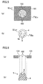
FIG. 5] FIG. 5(a) is a plan view illustrating a shape of a mask for forming a height adjusting portion on a columnar spacer.FIG. 5(b) is a plan view of the columnar spacer. - [
FIG. 6] FIG. 6(a) is a cross-sectional view along a VIa-Via line ofFIG. 5(a). FIG. 6(b) is a cross-sectional view along a VIb-VIb line ofFIG. 5(b) . - [
FIG. 7] FIG. 7 is a cross-sectional view of still another embodiment in which height adjusting portions are formed by using a photosensitive resist. - [
FIG. 8] FIG. 8 is a view of still another embodiment corresponding toFIG. 2 . - [
FIG. 9] FIG. 9 is a view of still another embodiment corresponding toFIG. 2 . - [
FIG. 10] FIG. 10 is a view of still another embodiment corresponding toFIG. 2 .FIG. 10(a) is a cross-sectional view along an Xa-Xa line ofFIG. 10(b) . - An embodiment of the present invention will be described below with reference to the drawings.
-
FIG. 1 illustrates a liquid crystal display device 1 of the embodiment of the present invention, and the liquid crystal display device 1 includes a pair ofsubstrates substrates color filter substrate 2 and anarray substrate 3, and a plurality ofcolumnar spacers 4 configured to maintain a constant gap G between the pair ofsubstrates color filter substrate 2. A liquid crystal material (not shown in the figure) is sealed in the gap G maintained constant by thecolumnar spacers 4. - As a feature of the present embodiment, the
columnar spacer 4 is in a conical trapezoidal shape and includes aheight adjusting portion 5 at a tip end contacting thearray substrate 3. The shape of the columnar spacer may be a quadrangular prism shape or a cylindrical shape as long as the height adjusting portion can be formed on an upper base thereof. Thecolumnar spacer 4 is formed by stacking colored layers or is made of a special material such as photosensitive polyimide, photosensitive acrylic region, and photosensitive colored resin by, e.g., photolithography, a dry film resist, or printing. The height of thecolumnar spacer 4 is, e.g., 3-10 µm, and the width of thecolumnar spacer 4 is, e.g., 10-50 µm. - Specifically, as illustrated in an enlarged view of
FIG. 2 , theheight adjusting portion 5 includes a plurality of protrusions (two protrusions in the present embodiment) provided on aflat surface 4a at the tip end of the conical trapezoidal portion of thecolumnar spacer 4, and the protrusions arehemispherical bodies 6. For example, a height h of thehemispherical body 6 is greater than 0 and equal to or less than 1.0 µm (0 < h ≤ 1.0 µm), and a width w1 (outer diameter) of thehemispherical body 6 is greater than 0 and equal to or less than a half of a tip end width w2 of the columnar spacer 4 (0 < w1 ≤ w2/2). By providing thehemispherical bodies 6, theheight adjusting portion 5 has a cross-sectional area smaller than that of the conical trapezoidal portion and stiffness less than that of the conical trapezoidal portion, and therefore is deformable when the pair ofsubstrates height adjusting portion 5 protruding beyond surroundings is deformed, thereby maintaining the constant gap G between the pair ofsubstrates - As illustrated in
FIG. 3 , a level of a surface of a base of thecolor filter substrate 2 is higher in a circumferential edge portion (edge portion 2a illustrated as a region B inFIG. 3 ) than in apixel portion 2b (illustrated as a region A inFIG. 3 ) provided on an inner side relative to theedge portion 2a, and a step is formed between a surface of theedge portion 2a and a surface of thepixel portion 2b. As a result, the height of thecolumnar spacer 4 provided in theedge portion 2a is higher than that of thecolumnar spacer 4 provided in thepixel portion 2b. For example, the height of the step is smaller than 1.0 µm. A deformation amount of theheight adjusting portion 5 of thecolumnar spacer 4 provided in theedge portion 2a is greater than that of theheight adjusting portion 5 of thecolumnar spacer 4 provided in thepixel portion 2b, thereby maintaining the constant gap G between the pair ofsubstrates - Next, a method for manufacturing the liquid crystal display device 1 according to the present embodiment will be described.
- First, a plurality of
columnar spacers 4 are formed on acolor filter substrate 2. In the present embodiment, thecolumnar spacers 4 andheight adjusting portions 5 are formed by, e.g., printing. - As the printing, there are techniques such as screen printing and flexography. As illustrated in, e.g.,
FIG. 4(a) , recesses 11 corresponding to conical trapezoidal portions of thecolumnar spacers 4 are formed in part of aprinting plate 10 corresponding to thecolumnar spacers 4 in advance, and a plurality ofhemispherical recesses 12 are formed in part of theprinting plate 10 corresponding to theflat surfaces 4a formed at the tip ends of the conical trapezoidal portions in advance. - Then, the screen printing or the flexography using the
printing plate 10 is performed on thecolor filter substrate 2. After a printed portion is cured, thecolumnar spacers 4 in each of which a plurality ofhemispherical bodies 6 protrude from theflat surface 4a as illustrated inFIG. 4(b) are formed corresponding to therecesses 11 and the hemispherical recesses 12. - As in the foregoing, since the plurality of
hemispherical recesses 12 are simply formed in positions of theprinting plate 10 corresponding to theheight adjusting portions 5 in advance, theheight adjusting portions 5 having a desired shape can be easily formed. In addition, in the present embodiment, since the plurality of protrusions are thehemispherical bodies 6, molding of such protrusions is facilitated. - As illustrated in
FIGS. 1(a) and3(a) , thecolor filter substrate 2 on which thecolumnar spacers 4 each including theheight adjusting portion 5 at the tip end thereof is bonded to anarray substrate 3 while applying pressure to thecolor filter substrate 2. - In the foregoing state, the height of the
columnar spacer 4 provided in anedge portion 2a is higher than that of thecolumnar spacer 4 provided in apixel portion 2b. Thus, when the pair ofsubstrates height adjusting portions 5 of thecolumnar spacers 4 provided in theedge portion 2a first contact thearray substrate 3. Since thehemispherical body 6 has stiffness less than that of the conical trapezoidal portion, thehemispherical bodies 6 are pressed and deformed. In such a state, deformation of theheight adjusting portions 5 of thecolumnar spacers 4 provided in theedge portion 2a is larger than that of theheight adjusting portions 5 of thecolumnar spacers 4 provided in thepixel portion 2b. In addition, even if thecolumnar spacers 4 provided in theedge portion 2a or thecolumnar spacers 4 provided in thepixel portion 2b are different from each other in height, theheight adjusting portion 5 provided at the tip end of the highercolumnar spacer 4 is first deformed by contacting a surface of thearray substrate 3. Then, by further pressing the pair ofsubstrates hemispherical bodies 6 protruding beyond othercolumnar spacers 4 are gradually pressed until the heights of all of thecolumnar spacers 4 are uniformized. In such a manner, a constant gap G between the pair ofsubstrates - The height of the
height adjusting portion 5 is greater than 0 and equal to or less than 1.0 µm, and the width w1 of theheight adjusting portion 5 is greater than 0 and equal to or less than the half of the tip end width w2 of the columnar spacer 4 (0 < w1 ≤ w2/2). Thus, an appropriate difference between stiffness of theheight adjusting portion 5 maintained at the minimum height and width and stiffness of theflat surface 4a of thecolumnar spacer 4 is maintained, thereby realizing easy height adjustment. - Then, the constant gap G is filled with a liquid crystal material.
- According to the liquid crystal display device 1 of the present embodiment, the
height adjusting portion 5 is provided in thecolumnar spacer 4, and theheight adjusting portion 5 is deformable when the pair ofsubstrates substrates -
FIGS. 5 and 6 illustrate an exposure process for forming a liquid crystal display device 1 of a first variation of the present embodiment, and the first variation of the present embodiment is different from the foregoing embodiment in a method for forming aheight adjusting portion 5. The same reference numerals as those shown inFIGS. 1-3 are used to represent equivalent elements in each of variations described below, and the detailed description thereof will not be repeated. - When columnar spacers are formed by photolithography using a negative photosensitive resist, a
columnar spacer 4 having theheight adjusting portion 5 is formed by performing the exposure process in a state in which a light shielding film is not provided in aportion 102 of anexposure mask 101 corresponding to theheight adjusting portion 5 and a semi-transmissive film or a transmissive film is provided in the remainingportion 103 corresponding to thecolumnar spacer 4. - As in the foregoing, a photosensitive amount is adjusted partially in the
exposure mask 101 by using a transmittance difference, and therefore theheight adjusting portion 5 can be easily formed so as to protrude from a tip end of thecolumnar spacer 4. -
FIG. 7 illustrates a cross section of a dry film resist 201 used for forming a liquid crystal display device 1 of a second variation of the embodiment of the present invention. - In the present variation,
columnar spacers 4 andheight adjusting portions 5 are formed by the dry film resist 201. Specifically, thecolumnar spacers 4 and theheight adjusting portions 5 are formed, e.g., by arranging a plurality ofrecesses 203 at regular intervals in aprotective film 202 of the dry film resist 201 in advance. Note that the dry film resist 201 is supported by asupport film 204. - The plurality of
recesses 203 are provided in portions of the protective film corresponding to theheight adjusting portions 5 in advance as in the foregoing, and therefore easy formation of theheight adjusting portions 5 having a desired shape in a proper position can be ensured by simply exposing portions corresponding to thecolumnar spacers 4 with light without processing theexposure mask 101 to form theheight adjusting portions 5 as in the first variation. - In the present variation, since a plurality of protrusions are
hemispherical bodies 6, molding of such protrusions is facilitated. - The foregoing embodiment of the present invention may have the following configurations.
- That is, in the foregoing embodiment, the plurality of protrusions provided in the rectangular
columnar spacer 4 are the twohemispherical bodies 6, but the number of the protrusions is not limited. The plurality of protrusions may be, e.g., fourquadrangular pyramids 106 as illustrated inFIG. 8 , or may be, e.g., fourtriangular pyramids 206 as illustrated inFIG. 9 . If the plurality of protrusions are thequadrangular pyramids 106, thetriangular pyramids 206, or pyramids such as cones, a tip end thereof is sharpened as compared to thehemispherical bodies 6 and columnar bodies. Thus, the tip end of the protrusion is easily deformed with small force, thereby obtaining the suitableheight adjusting portion 5. Note that, in any of the foregoing shapes, the height of the protrusion may be greater than 0 and equal to or less than 1.0 µm, and the width of the protrusion may be greater than 0 and equal to or less than the half of the tip end width of thecolumnar spacer 4. - As illustrated in
FIG. 10 , the plurality of protrusions may include a centerhemispherical body 6 and acircular body 306 surrounding thehemispherical body 6. Alternatively, thehemispherical body 6 may be a smallcircular body 306. In such a case, theheight adjusting portion 5 can be obtained, which can be molded by the photolithography and is easily deformed with a simple configuration. - Although not shown in the figure, the plurality of protrusions may be columnar bodies. In such a case, since an increase/decrease in cross-sectional area is less likely to occur, the columnar body is suitable for molding by the photolithography.
- As described above, the shape of the plurality of protrusions is not limited, and the number of the plurality of protrusions are not also limited as long as two or more protrusions are formed.
- Note that the foregoing embodiments have been set forth merely for purposes of preferred examples in nature, and are not intended to limit the present invention or the application or scope thereof.
- As described above, the present invention is useful for the liquid crystal display device including the plurality of columnar spacers provided in one of the pair of substrates, i.e., one of the color filter substrate or the array substrate and configured to maintain the constant gap between the pair of substrates, and to the method for manufacturing the liquid crystal display device.
-
- 1
- Liquid Crystal Display Device
- 2
- Color Filter Substrate (One of a Pair of Substrates)
- 2a
- Edge Portion (Step)
- 3
- Array Substrate (The Other Substrate)
- 4
- Columnar Spacer
- 5
- Height Adjusting Portion
- 6
- Hemispherical Body (Protrusion)
- 12
- Hemispherical Recesses
- 101
- Exposure Mask
- 106
- Quadrangular Pyramid (Protrusion)
- 201
- Dry Film Resist
- 202
- Protective Film
- 203
- Recesses
- 206
- Triangular Pyramid (Protrusion)
- 306
- Circular Body (Protrusion)
Claims (13)
- A liquid crystal display device, comprising:a plurality of columnar spacers provided on one of a pair of substrates and configured to maintain a constant gap between the pair of substrates,wherein each of the columnar spacers includes, at a tip end contacting the other substrate, a height adjusting portion which is easily deformed as compared to other portion of the columnar spacer when the pair of substrates are bonded together.
- A liquid crystal display device, comprising:a plurality of columnar spacers provided on one of a pair of substrates and configured to maintain a constant gap between the pair of substrates,wherein each of the columnar spacers includes a height adjusting portion at a tip end contacting the other substrate, andthe height adjusting portion is deformed when the pair of substrates are bonded together, thereby maintaining the constant gap.
- The liquid crystal display device of claim 1 or 2, wherein
a step is formed on a surface of a base of the one of the pair of substrates, and
a deformation amount of the height adjusting portion of the columnar spacer provided in a region on a higher side of the step is greater than a deformation amount of the height adjusting portion of the columnar spacer provided in a region on a lower side of the step. - The liquid crystal display device of any one of claims 1-3, wherein
a height of the height adjusting portion is greater than 0 and equal to or less than 1.0 µm, and
a width of the height adjusting portion is greater than 0 and equal to or less than a half of a tip end width of the columnar spacer. - The liquid crystal display device of any one of claims 1-4, wherein
the height adjusting portion includes a plurality of protrusions protruding from the tip end of the columnar spacer. - The liquid crystal display device of claim 5, wherein
the plurality of protrusions are hemispherical bodies. - The liquid crystal display device of claim 5, wherein
the plurality of protrusions are columnar bodies. - The liquid crystal display device of claim 5, wherein
the plurality of protrusions are pyramids. - The liquid crystal display device of claim 5, wherein
the plurality of protrusions are circular bodies. - A method for manufacturing a liquid crystal display device including a plurality of columnar spacers provided on one of a pair of substrates and configured to maintain a constant gap between the pair of substrates, the method comprising:forming the columnar spacers each including a height adjusting portion at a tip end contacting the other substrate; andbonding the one of the pair of substrates including the columnar spacers to the other substrate while deforming the height adjusting portions, thereby maintaining the constant gap.
- The method of claim 10, wherein
the columnar spacers each having the height adjusting portion is formed by performing an exposure process by photolithography in a state in which a light shielding film is not provided in portions of an exposure mask corresponding to the height adjusting portions and a semi-transmissive film or a transmissive film is provided in the remaining portions corresponding to the columnar spacers. - The method of claim 10, wherein
a plurality of recesses are formed in a protective film of a dry film resist in advance, thereby forming the height adjusting portions. - The method of claim 10, wherein
a plurality of recesses are formed in part of a printing plate corresponding to tip ends of the columnar spacers in advance, thereby forming the columnar spacers each having the height adjusting portion.
Applications Claiming Priority (2)
| Application Number | Priority Date | Filing Date | Title |
|---|---|---|---|
| JP2009143021 | 2009-06-16 | ||
| PCT/JP2010/000391 WO2010146729A1 (en) | 2009-06-16 | 2010-01-25 | Liquid crystal display element and manufacturing method thereof |
Publications (2)
| Publication Number | Publication Date |
|---|---|
| EP2444837A1 true EP2444837A1 (en) | 2012-04-25 |
| EP2444837A4 EP2444837A4 (en) | 2014-01-22 |
Family
ID=43356066
Family Applications (1)
| Application Number | Title | Priority Date | Filing Date |
|---|---|---|---|
| EP10789114.5A Withdrawn EP2444837A4 (en) | 2009-06-16 | 2010-01-25 | Liquid crystal display element and manufacturing method thereof |
Country Status (7)
| Country | Link |
|---|---|
| US (1) | US20120086901A1 (en) |
| EP (1) | EP2444837A4 (en) |
| JP (1) | JP5318953B2 (en) |
| CN (1) | CN102804046A (en) |
| BR (1) | BRPI1014243A2 (en) |
| RU (1) | RU2495464C2 (en) |
| WO (1) | WO2010146729A1 (en) |
Cited By (1)
| Publication number | Priority date | Publication date | Assignee | Title |
|---|---|---|---|---|
| KR20210122410A (en) * | 2020-03-31 | 2021-10-12 | 삼성디스플레이 주식회사 | Display device and method for manufacturing of the same |
Families Citing this family (12)
| Publication number | Priority date | Publication date | Assignee | Title |
|---|---|---|---|---|
| JP5917126B2 (en) | 2011-12-19 | 2016-05-11 | 株式会社ジャパンディスプレイ | Liquid crystal display |
| CN103076700B (en) * | 2013-02-18 | 2015-11-25 | 合肥京东方光电科技有限公司 | Liquid crystal panel and display device |
| CN103235450B (en) * | 2013-03-15 | 2015-12-02 | 合肥京东方光电科技有限公司 | Display panel and preparation method thereof, mask plate and preparation method thereof, display device |
| KR20150040648A (en) * | 2013-10-07 | 2015-04-15 | 삼성디스플레이 주식회사 | LIQUID CRYSTAL DISPlAY |
| CN104238197B (en) * | 2014-07-24 | 2017-06-16 | 合肥鑫晟光电科技有限公司 | A kind of chock insulator matter, display panel and display device |
| US9383609B2 (en) * | 2014-11-14 | 2016-07-05 | Sharp Kabushiki Kaisha | Liquid crystal display device |
| CN104898329A (en) * | 2015-06-24 | 2015-09-09 | 深圳市华星光电技术有限公司 | Method for manufacturing liquid crystal panel |
| CN105093706A (en) * | 2015-08-13 | 2015-11-25 | 京东方科技集团股份有限公司 | Spacer, masking plate, display panel and display device |
| CN105259713B (en) * | 2015-11-20 | 2018-09-14 | 武汉华星光电技术有限公司 | Curved surface liquid crystal panel and curved surface liquid crystal display device |
| KR102343241B1 (en) * | 2017-07-24 | 2021-12-27 | 삼성디스플레이 주식회사 | Display device and fabrication method of the same |
| CN112083606A (en) * | 2019-06-14 | 2020-12-15 | 夏普株式会社 | Liquid crystal display device and method for manufacturing liquid crystal display device |
| CN116206538A (en) * | 2021-12-01 | 2023-06-02 | 海信视像科技股份有限公司 | Display screen |
Family Cites Families (20)
| Publication number | Priority date | Publication date | Assignee | Title |
|---|---|---|---|---|
| JP3241142B2 (en) * | 1993-01-20 | 2001-12-25 | 大日本印刷株式会社 | Method for producing decorative decorative sheet having uneven pattern and mirror gloss and painted molded article |
| KR970048809A (en) * | 1995-12-30 | 1997-07-29 | 손욱 | LCD with Elastic Adhesive Spacers |
| JP3458620B2 (en) * | 1996-10-03 | 2003-10-20 | 東レ株式会社 | Liquid crystal display device substrate and liquid crystal display device |
| JP3196744B2 (en) * | 1998-11-20 | 2001-08-06 | 日本電気株式会社 | Liquid crystal display device and method of manufacturing the same |
| EP1048972A3 (en) * | 1999-04-30 | 2004-03-10 | Matsushita Electric Industrial Co., Ltd. | Liquid crystal display element and manufacturing method thereof |
| JP2001013506A (en) * | 1999-04-30 | 2001-01-19 | Matsushita Electric Ind Co Ltd | Liquid crystal display device and method of manufacturing the same |
| JP3680730B2 (en) * | 2000-12-08 | 2005-08-10 | 株式会社日立製作所 | Liquid crystal display |
| JP4474098B2 (en) | 2002-12-19 | 2010-06-02 | 奇美電子股▲ふん▼有限公司 | Image display device |
| JP4929578B2 (en) * | 2003-11-10 | 2012-05-09 | 大日本印刷株式会社 | Liquid crystal display |
| JP4044090B2 (en) * | 2003-12-26 | 2008-02-06 | シャープ株式会社 | Color filter substrate, liquid crystal display device including the same, and method for manufacturing color filter substrate |
| TWI247959B (en) * | 2004-01-30 | 2006-01-21 | Chi Mei Optoelectronics Corp | Liquid crystal display device |
| KR100672652B1 (en) * | 2004-04-30 | 2007-01-24 | 엘지.필립스 엘시디 주식회사 | Liquid crystal display and manufacturing method thereof |
| US7433004B2 (en) * | 2004-06-11 | 2008-10-07 | Sharp Kabushiki Kaisha | Color filter substrate, method of making the color filter substrate and display device including the color filter substrate |
| TWI313765B (en) * | 2005-01-27 | 2009-08-21 | Au Optronics Corp | Liquid crystal display panel and fabrication method thereof |
| JP2006330031A (en) * | 2005-05-23 | 2006-12-07 | Sanyo Epson Imaging Devices Corp | Liquid crystal display, manufacturing method of liquid crystal display and electronic device |
| JP4623043B2 (en) * | 2007-04-11 | 2011-02-02 | 日立化成工業株式会社 | Liquid crystal display device |
| JP2008292640A (en) * | 2007-05-23 | 2008-12-04 | Mitsubishi Electric Corp | Display device and manufacturing method thereof |
| JP5122867B2 (en) * | 2007-05-24 | 2013-01-16 | 株式会社東芝 | Liquid crystal display panel, liquid crystal display panel manufacturing method, liquid crystal display device, and liquid crystal display device manufacturing method |
| JP5315646B2 (en) * | 2007-08-30 | 2013-10-16 | 凸版印刷株式会社 | Manufacturing method of color filter |
| JP2009258374A (en) * | 2008-04-16 | 2009-11-05 | Hitachi Chem Co Ltd | Liquid crystal spacer and production method of the same, photosensitive resin composition, photosensitive element, and liquid crystal display device |
-
2010
- 2010-01-25 CN CN2010800268316A patent/CN102804046A/en active Pending
- 2010-01-25 WO PCT/JP2010/000391 patent/WO2010146729A1/en not_active Ceased
- 2010-01-25 RU RU2011152315/28A patent/RU2495464C2/en not_active IP Right Cessation
- 2010-01-25 JP JP2011519470A patent/JP5318953B2/en not_active Expired - Fee Related
- 2010-01-25 BR BRPI1014243A patent/BRPI1014243A2/en not_active IP Right Cessation
- 2010-01-25 EP EP10789114.5A patent/EP2444837A4/en not_active Withdrawn
- 2010-01-25 US US13/378,945 patent/US20120086901A1/en not_active Abandoned
Cited By (1)
| Publication number | Priority date | Publication date | Assignee | Title |
|---|---|---|---|---|
| KR20210122410A (en) * | 2020-03-31 | 2021-10-12 | 삼성디스플레이 주식회사 | Display device and method for manufacturing of the same |
Also Published As
| Publication number | Publication date |
|---|---|
| WO2010146729A1 (en) | 2010-12-23 |
| EP2444837A4 (en) | 2014-01-22 |
| RU2495464C2 (en) | 2013-10-10 |
| BRPI1014243A2 (en) | 2019-09-24 |
| RU2011152315A (en) | 2013-07-27 |
| CN102804046A (en) | 2012-11-28 |
| US20120086901A1 (en) | 2012-04-12 |
| JP5318953B2 (en) | 2013-10-16 |
| JPWO2010146729A1 (en) | 2012-11-29 |
Similar Documents
| Publication | Publication Date | Title |
|---|---|---|
| EP2444837A1 (en) | Liquid crystal display element and manufacturing method thereof | |
| US9140934B2 (en) | Liquid crystal display | |
| CN103439836B (en) | A kind of chock insulator matter and preparation method thereof, liquid crystal panel | |
| US7884917B2 (en) | Spacer and liquid crystal display panel with the same | |
| US6750938B2 (en) | Liquid crystal display device and liquid crystal display apparatus incorporating the same | |
| CN106597759B (en) | Spacer, display substrate and manufacturing method thereof, and display panel | |
| CN103268037A (en) | Color filter substrate, manufacturing method of color filter substrate and display device | |
| TW201423239A (en) | Flexible display and manufacturing method thereof | |
| CN111427198A (en) | Display substrate, method for producing the same, and display device | |
| CN205563031U (en) | Color filter substrate and display panel | |
| US7924358B2 (en) | Spacer structure of a display panel | |
| CN111045259A (en) | Display panel and method of making the same | |
| US20190258104A1 (en) | Vertical alignment display panel and display apparatus | |
| JP2000019534A (en) | Method for assembling stressless liquid crystal cell and its device | |
| CN104216161B (en) | A kind of display device | |
| US20210011323A1 (en) | Manufacturing method of liquid crystal cell | |
| CN103760720A (en) | Display panel, manufacturing method thereof and display device | |
| US10935833B2 (en) | Display apparatus and display substrate having a display area and a black matrix area, and method of fabricating display substrate and display apparatus | |
| KR100904698B1 (en) | Light control film and its manufacturing method | |
| JP4099947B2 (en) | Liquid crystal display | |
| CN115826301A (en) | Liquid crystal display panel, manufacturing method thereof, and liquid crystal display device | |
| CN211741793U (en) | Display substrate and display device | |
| JP2010181640A (en) | Liquid crystal display panel and method for manufacturing liquid crystal display panel | |
| CN113608382A (en) | Array substrate, manufacturing method thereof and display panel | |
| US7471370B2 (en) | Columnar spacer for liquid crystal display |
Legal Events
| Date | Code | Title | Description |
|---|---|---|---|
| PUAI | Public reference made under article 153(3) epc to a published international application that has entered the european phase |
Free format text: ORIGINAL CODE: 0009012 |
|
| 17P | Request for examination filed |
Effective date: 20111214 |
|
| AK | Designated contracting states |
Kind code of ref document: A1 Designated state(s): AT BE BG CH CY CZ DE DK EE ES FI FR GB GR HR HU IE IS IT LI LT LU LV MC MK MT NL NO PL PT RO SE SI SK SM TR |
|
| RIN1 | Information on inventor provided before grant (corrected) |
Inventor name: NAKAGAWA, AKIRA Inventor name: KOHARA, YASUHIRO |
|
| DAX | Request for extension of the european patent (deleted) | ||
| RIC1 | Information provided on ipc code assigned before grant |
Ipc: G09F 9/30 20060101ALI20131212BHEP Ipc: G02F 1/1339 20060101AFI20131212BHEP |
|
| A4 | Supplementary search report drawn up and despatched |
Effective date: 20131220 |
|
| STAA | Information on the status of an ep patent application or granted ep patent |
Free format text: STATUS: THE APPLICATION HAS BEEN WITHDRAWN |
|
| 18W | Application withdrawn |
Effective date: 20140129 |