EP2443594B1 - Resistive assessment of the coupling coefficient of an electromagnetic transponder - Google Patents
Resistive assessment of the coupling coefficient of an electromagnetic transponder Download PDFInfo
- Publication number
- EP2443594B1 EP2443594B1 EP10734222.2A EP10734222A EP2443594B1 EP 2443594 B1 EP2443594 B1 EP 2443594B1 EP 10734222 A EP10734222 A EP 10734222A EP 2443594 B1 EP2443594 B1 EP 2443594B1
- Authority
- EP
- European Patent Office
- Prior art keywords
- transponder
- terminal
- value
- coupling
- voltage
- Prior art date
- Legal status (The legal status is an assumption and is not a legal conclusion. Google has not performed a legal analysis and makes no representation as to the accuracy of the status listed.)
- Active
Links
Images

Classifications
-
- G—PHYSICS
- G06—COMPUTING; CALCULATING OR COUNTING
- G06K—GRAPHICAL DATA READING; PRESENTATION OF DATA; RECORD CARRIERS; HANDLING RECORD CARRIERS
- G06K19/00—Record carriers for use with machines and with at least a part designed to carry digital markings
- G06K19/06—Record carriers for use with machines and with at least a part designed to carry digital markings characterised by the kind of the digital marking, e.g. shape, nature, code
- G06K19/067—Record carriers with conductive marks, printed circuits or semiconductor circuit elements, e.g. credit or identity cards also with resonating or responding marks without active components
- G06K19/07—Record carriers with conductive marks, printed circuits or semiconductor circuit elements, e.g. credit or identity cards also with resonating or responding marks without active components with integrated circuit chips
- G06K19/0723—Record carriers with conductive marks, printed circuits or semiconductor circuit elements, e.g. credit or identity cards also with resonating or responding marks without active components with integrated circuit chips the record carrier comprising an arrangement for non-contact communication, e.g. wireless communication circuits on transponder cards, non-contact smart cards or RFIDs
-
- G—PHYSICS
- G06—COMPUTING; CALCULATING OR COUNTING
- G06K—GRAPHICAL DATA READING; PRESENTATION OF DATA; RECORD CARRIERS; HANDLING RECORD CARRIERS
- G06K19/00—Record carriers for use with machines and with at least a part designed to carry digital markings
- G06K19/06—Record carriers for use with machines and with at least a part designed to carry digital markings characterised by the kind of the digital marking, e.g. shape, nature, code
- G06K19/067—Record carriers with conductive marks, printed circuits or semiconductor circuit elements, e.g. credit or identity cards also with resonating or responding marks without active components
- G06K19/07—Record carriers with conductive marks, printed circuits or semiconductor circuit elements, e.g. credit or identity cards also with resonating or responding marks without active components with integrated circuit chips
- G06K19/0701—Record carriers with conductive marks, printed circuits or semiconductor circuit elements, e.g. credit or identity cards also with resonating or responding marks without active components with integrated circuit chips at least one of the integrated circuit chips comprising an arrangement for power management
- G06K19/0702—Record carriers with conductive marks, printed circuits or semiconductor circuit elements, e.g. credit or identity cards also with resonating or responding marks without active components with integrated circuit chips at least one of the integrated circuit chips comprising an arrangement for power management the arrangement including a battery
-
- G—PHYSICS
- G06—COMPUTING; CALCULATING OR COUNTING
- G06K—GRAPHICAL DATA READING; PRESENTATION OF DATA; RECORD CARRIERS; HANDLING RECORD CARRIERS
- G06K19/00—Record carriers for use with machines and with at least a part designed to carry digital markings
- G06K19/06—Record carriers for use with machines and with at least a part designed to carry digital markings characterised by the kind of the digital marking, e.g. shape, nature, code
- G06K19/067—Record carriers with conductive marks, printed circuits or semiconductor circuit elements, e.g. credit or identity cards also with resonating or responding marks without active components
- G06K19/07—Record carriers with conductive marks, printed circuits or semiconductor circuit elements, e.g. credit or identity cards also with resonating or responding marks without active components with integrated circuit chips
- G06K19/0701—Record carriers with conductive marks, printed circuits or semiconductor circuit elements, e.g. credit or identity cards also with resonating or responding marks without active components with integrated circuit chips at least one of the integrated circuit chips comprising an arrangement for power management
- G06K19/0715—Record carriers with conductive marks, printed circuits or semiconductor circuit elements, e.g. credit or identity cards also with resonating or responding marks without active components with integrated circuit chips at least one of the integrated circuit chips comprising an arrangement for power management the arrangement including means to regulate power transfer to the integrated circuit
-
- G—PHYSICS
- G06—COMPUTING; CALCULATING OR COUNTING
- G06K—GRAPHICAL DATA READING; PRESENTATION OF DATA; RECORD CARRIERS; HANDLING RECORD CARRIERS
- G06K19/00—Record carriers for use with machines and with at least a part designed to carry digital markings
- G06K19/06—Record carriers for use with machines and with at least a part designed to carry digital markings characterised by the kind of the digital marking, e.g. shape, nature, code
- G06K19/067—Record carriers with conductive marks, printed circuits or semiconductor circuit elements, e.g. credit or identity cards also with resonating or responding marks without active components
- G06K19/07—Record carriers with conductive marks, printed circuits or semiconductor circuit elements, e.g. credit or identity cards also with resonating or responding marks without active components with integrated circuit chips
- G06K19/0723—Record carriers with conductive marks, printed circuits or semiconductor circuit elements, e.g. credit or identity cards also with resonating or responding marks without active components with integrated circuit chips the record carrier comprising an arrangement for non-contact communication, e.g. wireless communication circuits on transponder cards, non-contact smart cards or RFIDs
- G06K19/0726—Record carriers with conductive marks, printed circuits or semiconductor circuit elements, e.g. credit or identity cards also with resonating or responding marks without active components with integrated circuit chips the record carrier comprising an arrangement for non-contact communication, e.g. wireless communication circuits on transponder cards, non-contact smart cards or RFIDs the arrangement including a circuit for tuning the resonance frequency of an antenna on the record carrier
Definitions
- the present invention generally relates to electronic systems and more particularly to systems using electromagnetic transponders, that is to say transceivers that can be interrogated without contact and wirelessly by a reading terminal and / or writing.
- Communication systems based on a modulation of an electromagnetic field generated by a terminal are multiple. This ranges from a simple electronic tag used as an antitheft device to more complex systems where a transponder, having to communicate with the terminal in whose field it is, is equipped with calculation functions (electronic wallet for example) or with processing. of information.
- the electromagnetic transponder systems are based on the use of oscillating circuits comprising an antenna winding, transponder side and terminal side. These circuits are intended to be coupled by close magnetic field when the transponder enters the field of the terminal.
- the oscillating circuits of the terminal and the transponder are generally tuned to the same frequency corresponding to the excitation frequency of the oscillating circuit of the terminal.
- the transponders are devoid of autonomous power supply and extract the power required for the circuits they comprise of the high frequency field radiated by the antenna of the terminal.
- the quality of the communication and the possible transfer of energy depends on the coupling between the terminal and the transponder.
- This coupling which is inversely proportional (non-linear) to the distance between the terminal and the transponder, conditions the amplitude of the voltage recovered by the transponder. There is therefore a need to be able to evaluate the current coupling factor between a transponder and a terminal in the field of which it is located.
- the transponder recovers a supply voltage that strongly depends on the coupling, and therefore the consumption of the transponder circuits. For example, a decrease in the load (transponder consumption) leads to an increase in voltage and remote power. Depending on the current value of the coupling with respect to the optimum coupling, it may occur that a decrease in the load causes the coupling to approach the critical optimum coupling.
- the transponder is then in a paradoxical situation where its circuits consume less but where the voltage and remote power supply reach a maximum. For a current coupling k close to the optimum coupling, this maximum of remotely powered power is not consumed by the transponder circuits and the power must therefore be dissipated in the resonant circuit, causing the antenna to overheat. This overheating can even cause the disconnection of the contacts of the antenna, thus the destruction of the transponder.
- a conventional solution consists in detuning the transponder when the voltage at the terminals of the oscillating circuit exceeds a threshold.
- the document GB-A-2321725 discloses a method for dissipating excessive power received by a non-contact device.
- the document EP-A-1045325 discloses a distance detection method between an electromagnetic transponder and a terminal.
- An electromagnetic transponder as defined in claim 5 is also provided.
- the figure 1 is a block diagram of an electromagnetic transponder communication system.
- a terminal 1 (TERMINAL) is capable of communicating in the near field (for example according to an NFC protocol - Near Field Communication) with a remote element, namely a transponder 2 (TRANS).
- TERMINAL a terminal 1
- TRANS transponder 2
- the terminal can take various forms, for example, a ticket validation terminal, an electronic passport reader, a laptop, a mobile communication device (cellular phone, personal digital assistant - PDA, etc.), a box electronic starting of a motor vehicle, etc.
- a ticket validation terminal an electronic passport reader
- a laptop a mobile communication device (cellular phone, personal digital assistant - PDA, etc.), a box electronic starting of a motor vehicle, etc.
- the transponder can also take different forms, for example, a smart card, an electronic transport ticket, an electronic passport, a telecommunication terminal (cell phone, PDA, etc.), an electronic tag, etc.
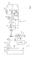
- the figure 2 represents, very schematically and simplified, an example of terminal 1 and transponder 2.
- the terminal 1 comprises an oscillating circuit, generally series, formed of an inductance L1 in series with a capacitor C1 and a resistor R1.
- This series oscillating circuit is, in the example of the figure 2 connected between an output terminal 12 of an antenna amplifier or coupler 14 and a terminal 13 at a reference potential (generally ground).
- An element 15 for measuring the current in the oscillating circuit is interposed, for example, between the capacitive element C1 and the ground 13. This measuring element 15 is part of a phase control loop which will be described later.
- the amplifier 14 receives a high frequency transmission signal from a modulator 16 (MOD) which receives a reference frequency (OSC signal) for example from a quartz oscillator (not shown).
- MOD modulator 16
- OSC signal reference frequency
- the modulator 16 receives, if necessary, a signal Tx coming from a control circuit 11 for controlling and operating the transmissions.
- This circuit 11 is generally provided with a microprocessor for processing commands and data, communicating with different input / output circuits (keyboard, screen, exchange element with a server, etc.) and / or non-detailed processing .
- the elements of the terminal 1 derive most often the energy necessary for their operation from a supply circuit (not shown) connected, for example, to the electrical distribution network (mains) or to a battery (for example, that of 'a motor vehicle or a phone or laptop).
- the modulator 16 provides a high frequency carrier (for example, at 13.56 MHz) to the L1-C1 series oscillating circuit which generates a magnetic field.
- the capacitive element C1 is, for example, a variable capacitance element and controllable by a CTRL signal. This element participates in the phase regulation of the current I1 in the antenna L1 with respect to a reference signal.
- This regulation is a regulation of the high frequency signal, that is to say the signal of the carrier corresponding to the signal supplied to the amplifier 14 in the absence of Tx data to be transmitted.
- the regulation is performed by varying the capacitance C1 of the oscillating circuit of the terminal so as to maintain the current in the antenna in constant phase relation with a reference signal.
- This reference signal corresponds, for example, to the signal OSC supplied to the modulator 14.
- the signal CTRL comes from a circuit 17 (COMP) whose role is to detect the phase difference with respect to the reference signal and to modify accordingly the capacity of the element C1.
- the comparator receives a MES information on the current I1 in the oscillating circuit detected by the measuring element 15 (for example, an intensity transformer or a resistor).
- a transponder 2 capable of cooperating with the terminal 1, comprises an oscillating circuit, for example a parallel circuit, formed of an inductor L2 in parallel with a capacitor C2 between two terminals 21 and 22.
- the parallel oscillating circuit (called the resonant circuit on reception ) is intended to capture the magnetic field generated by the oscillating circuit L1-C1 of the terminal 1.
- the circuits L2-C2 and L1-C1 are tuned to the same resonance frequency (for example 13.56 MHz).
- the terminals 21 and 22 are connected to two alternative input terminals of a rectifier bridge 23 (usually double alternation).
- the rectified output terminals of the bridge 23 respectively define a positive terminal 24 and a reference terminal 25.
- a capacitor Ca is connected between the terminals 24 and 25 so as to smooth the rectified voltage. If necessary, the recovered energy is used to recharge a battery not shown.
- a high frequency voltage is generated at the terminals of the resonant circuit L2-C2.
- This voltage rectified by the bridge 23 and smoothed by the capacitor Ca, supplies a supply voltage to electronic circuits of the transponder via a voltage regulator 26 (REG).
- These circuits generally comprise a processing unit 27 (for example a microcontroller ⁇ C) associated with a memory (not represented), a demodulator 28 (DEM) of the signals possibly received from the terminal 1, and a modulator 29 (MOD). to transmit information to the terminal.
- the transponder is generally synchronized by means of a clock (CLK) extracted, by a block 20, from the recovered high frequency signal, before rectification, on one of the terminals 21 or 22. Most commonly, all the electronic circuits of the transponder 2 are integrated in the same chip.
- CLK clock
- the circuit 16 modulates (generally in amplitude) the carrier (signal OSC) as a function of the signal Tx.
- these data are demodulated by the demodulator 28 from the voltage V Ca. If necessary, the demodulator takes the signal to be demodulated upstream of the rectifier bridge.
- the modulator 29 controls a modulation stage 30 (retromodulation) of the load formed by the transponder circuits on the magnetic field produced by the terminal.
- This stage generally consists of an electronic switch K30 (for example, a transistor) and a resistor R30 (or a capacitor), in series between the terminals 24 and 25.
- the switch K30 is controlled at a frequency (for example, 847.5 kHz) said subcarrier, significantly lower (usually with a ratio of at least 10) to the frequency of the excitation signal of the oscillating circuit of the terminal 1.
- the transponder oscillating circuit is subjected to additional damping with respect to the load formed by the circuits 20, 26, 27, 28, and 29 so that the transponder takes a larger amount of energy from the high frequency magnetic field.
- the amplifier 14 keeps the amplitude of the high frequency excitation signal constant. Consequently, the variation of energy of the transponder results in a variation of amplitude and phase of the current in the antenna L1. This variation is detected by an amplitude or phase demodulator of the terminal.
- the comparator 17 integrates a demodulator phase also used to demodulate the signal from the transponder. Therefore, this comparator 17 provides a signal Rx restoring a possible retromodulation of data received from a transponder to the circuit 11.
- Other demodulation circuits may be provided, for example a circuit using a measurement of the voltage across the capacitor C1 .
- the response time of the phase control loop is long enough not to hinder the possible retromodulation from a transponder, and sufficiently short in front of the speed of passage of a transponder in the field of the terminal.
- Static control over modulation frequencies can be used (for example, the 13.56 MHz remote power carrier frequency and the 847.5 kHz retrofit frequency used to transmit transponder data to the terminal).
- phase-regulated terminal An example of a phase-regulated terminal is described in the document EP-A-0 857 981 .
- the coupling coefficient between the oscillating circuit of the terminal and that of the transponder essentially depends on the distance separating the transponder from the terminal.
- k Opt The ⁇ 2 The ⁇ 1 ⁇ R ⁇ 1 R ⁇ 2 , where R2 represents the resistance equivalent to the load (load) constituted by the elements of the transponder on its own oscillating circuit.
- the resistor R2 represents the equivalent resistance of all the circuits (microprocessor, means of retromodulation, etc.) of the transponder 2, brought in parallel on the capacitor C2 and the inductance L2 (before or after the bridge rectifier ).
- resistive load the conductance provided by the transponder circuits, so their consumption.
- the level of this charge is symbolized by the resistance R2 in parallel across the oscillating circuit.
- the series resistance of inductance L1 terminal antenna
- the value of this series resistance is, for simplicity, included in the value of the resistor R1.
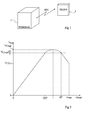
- the figure 3 represents an example of the shape of the voltage V C2 recovered on the transponder side as a function of the normalized coupling k / k opt with respect to the optimum coupling.
- the curve starts from the origin of ordinates (zero voltage) for a null coupling. This corresponds to a distance from the transponder and the terminal such that no signal is picked up by the transponder.
- V C2 I ⁇ 2 ⁇ ⁇ VS 2 , where 12 represents the current in the oscillating circuit of the transponder, and where ⁇ represents the pulse of the signal.
- I ⁇ 2 M ⁇ ⁇ ⁇ I ⁇ 1 Z ⁇ 2 , where I1 represents the current in the oscillating circuit of the terminal and where Z2 represents the impedance of the transponder.
- V C2tun is obtained when the latter is tuned, the formula :
- V VS ⁇ 2 k ⁇ The ⁇ 1 The ⁇ 2 ⁇ vg R ⁇ 1 R ⁇ 2 + k 2 ⁇ The ⁇ 1 The ⁇ 2 .
- V C2 (kopt) is therefore given by the formula (combining formulas 2 and 9):
- V VS ⁇ 2 ⁇ k opt vg 2 ⁇ R ⁇ 2 R ⁇ 1 .
- V VS ⁇ 2 2 ⁇ V VS ⁇ 2 ⁇ k opt k k Opt + k Opt k .
- This maximum power transferred from the terminal to the transponder is distributed between the resistor own losses in the resonant circuit and the resistor R2 corresponding to the consumption level of the transponder circuits.
- the current consumed becomes too low, it means that the value of R2 becomes very large and is therefore negligible compared with the resistor L2-C2 resonant circuit.
- the transferred power must be dissipated in this resistance of the LC circuit, which may damage the antenna.
- the figure 4 illustrates the effects of a detuning of the oscillating circuit according to the position of the coupling with respect to the optimum coupling.
- This figure shows examples of the steps of the voltage V C2 as a function of the value of the capacitor C2 for several coupling values k. It is assumed that the value of the resistance R2 does not vary.
- the maximum of the voltage V C2max is obtained at the tuning of the oscillating circuit (for simplicity, it is considered that any disagreement is caused only by a variation of the capacitance C2 and that the value of the inductance L2 remains fixed).
- the maximum voltage obtained is necessarily lower than the maximum voltage at the optimum coupling and decreases with respect to this value in case of disagreement with respect to the value C2 tun .
- the voltage V C2max can be reached even by detuning the circuit. Therefore, the disagreement of the oscillating circuit to protect from overheating is not always the solution.
- the oscillation circuit is detuned, preferably by changing the value of the capacitance C2. Indeed, it is easy to add or reduce the value of the capacitor by switching integrated capacitive elements in parallel with the capacitor C2.
- the transferred power is then partially dissipated in the resistor R2x, then reduced by detuning the oscillating circuit from k opt] R2x .
- the voltage at the terminals of the oscillating circuit is not measured directly, but the smoothed voltage across the capacitor V Ca at the output of the rectifier bridge 23.
- This voltage V Ca is proportional to the voltage V C2 .
- the measurement is performed by the microprocessor.
- the memorization of values of the measured voltages are effected, either analogically, but preferably numerically over several bits, the number of which depends on the desired analysis precision.
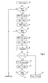
- the figure 5 is a flowchart illustrating an embodiment of the energy management method.
- the resistor R20 (block 47, R21-> R20) is preferably passed through.
- the ratio r is compared (block 49, h ⁇ r ⁇ H) with respect to two thresholds h and H to determine if it is within an acceptable range.
- Other values may be chosen provided, of course, that h is less than unity (preferably h is greater than 1/2) and H is greater than unity (preferably h is less than 10).
- the value of block R2x of resistance R2 is calculated (block 51, V C2opt] R2x ) according to formulas 20 and 21. to return the transponder to an optimum coupling position. Then (block 52, R20-> R2x), the value of the resistor R2 is changed to this estimated value.
- the resistive load is progressively increased by decreasing the value of R2 until the voltage V C2 reaches the value V C2opt] R2x calculated with the formula 20.
- the microcontroller interrogates a previously stored correspondence table (for example in a learning phase or during the design of the transponder) in order to know, from the value of the ratio r, the value to be given to the resistor R2.
- Test 45 is optional. Indeed, we can continue the execution of the process to move to the R2x resistor if the current coupling does not allow a disagreement. However, this test 45 makes it possible to exit the iteration more quickly if the resistance R21 proves to be sufficient.
- the figure 6 is a block diagram of an embodiment of a transponder 2, equipped to automatically determine, when in the field of a terminal (not shown), the current coupling with respect to the optimum coupling.
- the representation of the figure 6 is simplified compared to that of the figure 2 .
- the elements of demodulation, of retromodulation and of obtaining the clock frequency have not been illustrated.
- the consumption current I of the transponder circuit is measured by a resistor R sense mounted as a current detector.
- the measurement of the consumption current gives an indirect image of the equivalent resistance of the load.
- the measured value is less than or equal to the minimum value, the consumed current will be low and that, equivalently, the resistance is lower than the value R20.
- the current is lower than the minimum current, and the current coupling k is close to the optimum coupling, it is deduced that the transponder is in overheating conditions of the resonant circuit.
- the transponder 2 is based on a parallel oscillating circuit L2-C2 whose terminals 21 and 22 are connected to the input terminals of a rectifying bridge 23. Between the terminals 24 and 25 of the rectifying bridge 23 is provided a switchable resistive circuit 40. For example, two resistors R43 and R45 are connected in parallel each being in series with a switch K43, respectively K45. Switches K43 and K45 (for example, MOS transistors) are intended to be switched to implement the method of determining the coupling position.
- the processing unit 27 receives an information on the voltage V Ca on an input MES to implement the method described above.
- the resistor R2 (load of the transponder circuits) represents the value R20. Disconnection of one of the resistors (for example, resistor R43) increases resistance R2 to R21.
- Other connections and switches may be provided according to the variant of the method used. For example, a single switchable resistor can be used assuming that one of the two values of resistor R2 corresponds to the resistive load of the other transponder circuits.
- the switchable resistor corresponds to that used for resistive retromodulation.
- a first measurement is made by switching the retromodulation resistor so that it is functionally in the circuit (switch K30 in the on state in the example of FIG. figure 2 ).
- the voltage V C2] R20 is measured.
- the switch K30 is opened and the voltage V C2] R21 is measured.
- the implementation of the described method then requires no structural modification of a transponder equipped with a microcontroller. It is enough to program this microcontroller so that it switches the resistance of retromodulation.
- the thresholds used to determine the position with respect to the optimum coupling depend only on the values R20 and R21 which are known for a given transponder. Therefore, the transponder does not necessarily need advanced microprocessor-based computing means but can simply measure voltages, calculate the ratio and compare it against analog thresholds generated, for example, by resistive dividing bridges. In another example, the thresholds are precalculated and stored in a non-volatile memory of the transponder.
- the increase or decrease in the equivalent resistance R2 is caused by a variation of the consumption of the transponder circuits, typically of the processing unit 27.
- the increase or decrease in the equivalent resistance R2 is caused by a variation of the consumption of the transponder circuits, typically of the processing unit 27.
- the variation of the resistance R2 is known from the moment when the consumption of different tasks to be performed by the unit 27 is known, which is generally estimated at the transponder design or can be obtained in a learning phase with a any terminal.
- the calculations required to evaluate the current coupling are sufficiently simple so that their execution time is negligible compared to the speed of movement of a transponder in front of a terminal (thus the speed of variation of the coupling coefficient).
- the embodiments described are also applicable in the case where the transponder remains on a receiving surface of the terminal, the coupling does not vary throughout the communication.
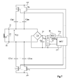
- the figure 7 represents an embodiment of a transponder equipped with a detuning circuit of the capacitor C2.
- the transponder 2 is based on a parallel oscillating circuit L2-C2 whose terminals 21 and 22 are connected to the input terminals of a rectifying bridge 23.
- the processing unit 27 receives information about the voltage V Ca on an input MES to implement the method described above.
- the transistors Ti are individually controllable by signals from the microcontroller 27 as a function of the measurements made conditioning the desired amplitude for the mismatch.
- switchable capacitors are connected in parallel to the oscillating circuit.
- an advantage of the solution of the figure 7 is that the transistors are more easily controllable because the control signals can be referenced to the ground.
- Coupling evaluation can be performed periodically during a communication. The only precaution is not to evaluate the coupling during a retromodulation of the transponder. A first evaluation is for example performed as soon as the energy recovered by the transponder is sufficient for the microprocessor 27 to operate. Then, periodic measurements are made during the communication.
Description
La présente invention concerne de façon générale les systèmes électroniques et plus particulièrement, les systèmes utilisant des transpondeurs électromagnétiques, c'est-à-dire des émetteurs-récepteurs susceptibles d'être interrogés sans contact et sans fil par un terminal de lecture et/ou d'écriture.The present invention generally relates to electronic systems and more particularly to systems using electromagnetic transponders, that is to say transceivers that can be interrogated without contact and wirelessly by a reading terminal and / or writing.
Les systèmes de communication basés sur une modulation d'un champ électromagnétique généré par un terminal sont multiples. Cela va de la simple étiquette électronique servant d'antivol à des systèmes plus complexes où un transpondeur, devant communiquer avec le terminal dans le champ duquel il se trouve, est équipé de fonctions de calcul (porte-monnaie électronique par exemple) ou de traitement d'information.Communication systems based on a modulation of an electromagnetic field generated by a terminal are multiple. This ranges from a simple electronic tag used as an antitheft device to more complex systems where a transponder, having to communicate with the terminal in whose field it is, is equipped with calculation functions (electronic wallet for example) or with processing. of information.
Les systèmes à transpondeurs électromagnétiques sont basés sur l'emploi de circuits oscillants comprenant un enroulement formant antenne, côté transpondeur et côté terminal. Ces circuits sont destinés à être couplés par champ magnétique proche lorsque le transpondeur entre dans le champ du terminal. Les circuits oscillants du terminal et du transpondeur sont généralement accordés sur une même fréquence correspondant à la fréquence d'excitation du circuit oscillant du terminal.The electromagnetic transponder systems are based on the use of oscillating circuits comprising an antenna winding, transponder side and terminal side. These circuits are intended to be coupled by close magnetic field when the transponder enters the field of the terminal. The oscillating circuits of the terminal and the transponder are generally tuned to the same frequency corresponding to the excitation frequency of the oscillating circuit of the terminal.
Dans la plupart des cas, les transpondeurs sont dépourvus d'alimentation autonome et extraient l'alimentation nécessaire aux circuits qu'ils comportent du champ haute fréquence rayonné par l'antenne du terminal.In most cases, the transponders are devoid of autonomous power supply and extract the power required for the circuits they comprise of the high frequency field radiated by the antenna of the terminal.
La qualité de la communication et de l'éventuel transfert d'énergie dépend du couplage entre le terminal et le transpondeur. Ce couplage, qui est inversement proportionnel (non linéaire) à la distance entre le terminal et le transpondeur, conditionne l'amplitude de la tension récupérée par le transpondeur. Il existe donc un besoin de pouvoir évaluer le facteur de couplage courant entre un transpondeur et un terminal dans le champ duquel il se trouve.The quality of the communication and the possible transfer of energy depends on the coupling between the terminal and the transponder. This coupling, which is inversely proportional (non-linear) to the distance between the terminal and the transponder, conditions the amplitude of the voltage recovered by the transponder. There is therefore a need to be able to evaluate the current coupling factor between a transponder and a terminal in the field of which it is located.
Le transpondeur récupère une tension d'alimentation qui dépend fortement du couplage, donc de la consommation des circuits du transpondeur. Par exemple, une diminution de la charge (consommation du transpondeur) entraine une augmentation de la tension et de la puissance téléalimentée. En fonction de la valeur courante du couplage par rapport au couplage optimum, il peut se produire qu'une diminution de la charge entraine que le couplage se rapproche du couplage optimum critique. Le transpondeur se trouve alors dans une situation paradoxale où ses circuits consomment moins mais où la tension et la puissance de téléalimentation atteignent un maximum. Pour un couplage courant k proche du couplage optimum, ce maximum de puissance téléalimentée n'est pas consommé par les circuits du transpondeur et la puissance doit donc être dissipée dans le circuit résonnant, entraînant une surchauffe de l'antenne. Cette surchauffe peut même provoquer la déconnection des contacts de l'antenne, donc la destruction du transpondeur.The transponder recovers a supply voltage that strongly depends on the coupling, and therefore the consumption of the transponder circuits. For example, a decrease in the load (transponder consumption) leads to an increase in voltage and remote power. Depending on the current value of the coupling with respect to the optimum coupling, it may occur that a decrease in the load causes the coupling to approach the critical optimum coupling. The transponder is then in a paradoxical situation where its circuits consume less but where the voltage and remote power supply reach a maximum. For a current coupling k close to the optimum coupling, this maximum of remotely powered power is not consumed by the transponder circuits and the power must therefore be dissipated in the resonant circuit, causing the antenna to overheat. This overheating can even cause the disconnection of the contacts of the antenna, thus the destruction of the transponder.
Une solution classique consiste à désaccorder le transpondeur quand la tension aux bornes du circuit oscillant excède un seuil.A conventional solution consists in detuning the transponder when the voltage at the terminals of the oscillating circuit exceeds a threshold.
Le fait de provoquer un désaccord risque d'aggraver la situation en augmentant la puissance téléalimentée. En effet, le désaccord peut être tel qu'il corresponde à un des maxima de puissance transférée pour la valeur désaccordée. Dans ce cas, le désaccord non seulement ne résout pas le problème, mais l'aggrave. Il en découle que modifier la charge du transpondeur en commutant une résistance en parallèle sur le circuit résonant ou en désaccordant ce dernier par une capacité commutable, sans connaître la position du couplage courant par rapport au couplage optimum, on a une chance sur deux d'empirer la situation.The fact of causing a disagreement may aggravate the situation by increasing the remote power supply. Indeed, the disagreement may be such that it corresponds to one of the maxima of transferred power for the detuned value. In this case, the disagreement not only does not solve the problem, but aggravates it. It follows that modifying the transponder load by switching a resistor in parallel to the resonant circuit or by detuning the latter by a switchable capacitor, without knowing the position of the current coupling with respect to the optimum coupling, one has a chance on two of make the situation worse.
Le document
Le document
Le document
Il serait souhaitable de pouvoir évaluer le facteur de couplage entre un transpondeur et un terminal.It would be desirable to be able to evaluate the coupling factor between a transponder and a terminal.
Il serait également souhaitable de pouvoir évaluer l'évolution de ce facteur de couplage lors d'une communication.It would also be desirable to be able to evaluate the evolution of this coupling factor during a communication.
Il serait également souhaitable de pouvoir évaluer le facteur de couplage sans qu'il soit nécessaire d'effectuer un échange de données entre le terminal et le transpondeur.It would also be desirable to be able to evaluate the coupling factor without the need for data exchange between the terminal and the transponder.
Il serait également souhaitable de pouvoir effectuer cette évaluation côté transpondeur.It would also be desirable to be able to perform this evaluation on the transponder side.
Il serait également souhaitable de proposer une solution indépendante du type de terminal dans le champ duquel se trouve le transpondeur.It would also be desirable to propose a solution independent of the type of terminal in whose field the transponder is located.
Pour atteindre tout ou partie de ces objets ainsi que d'autres, il est prévu un procédé de gestion de la puissance dans un transpondeur électromagnétique dans le champ d'un terminal telque défini dans la revendication 1.To achieve all or part of these objects as well as others, there is provided a power management method in an electromagnetic transponder in the field of a terminal as defined in
On prévoit également, un transpondeur électromagnétique telque défini dans la revendication 5.An electromagnetic transponder as defined in claim 5 is also provided.
D'autres modes de réalisations sont définis dans les revendications dépendantes.Other embodiments are defined in the dependent claims.
Ces objets, caractéristiques et avantages, ainsi que d'autres seront exposés en détail dans la description suivante de modes de réalisation particuliers faite à titre non-limitatif en relation avec les figures jointes parmi lesquelles :
- la
figure 1 est une représentation très schématique d'un système à transpondeur du type auquel s'applique à titre d'exemple la présente invention ; - la
figure 2 est un schéma bloc simplifié d'un terminal et d'un transpondeur d'un système de communication à transpondeur électromagnétique ; - la
figure 3 illustre un exemple d'allure de la tension aux bornes du circuit oscillant du transpondeur en fonction du facteur de couplage ; - la
figure 4 illustre, pour plusieurs facteurs de couplage, des exemples d'allure de la tension aux bornes du circuit oscillant du transpondeur en fonction de la valeur de sa capacité ; - la
figure 5 est un schéma bloc fonctionnel illustrant un mode de mise en oeuvre du procédé d'évaluation du facteur de couplage ; - la
figure 6 est un schéma bloc d'un mode de réalisation d'un transpondeur adapté à la mise en oeuvre du procédé ; et - la
figure 7 est un schéma bloc d'un autre mode de réalisation d'un transpondeur adapté à la mise en oeuvre du procédé.
- the
figure 1 is a very schematic representation of a transponder system of the type to which the present invention applies by way of example; - the
figure 2 is a simplified block diagram of a terminal and a transponder of an electromagnetic transponder communication system; - the
figure 3 illustrates an example of the shape of the voltage across the oscillating circuit of the transponder as a function of the coupling factor; - the
figure 4 illustrates, for several coupling factors, examples of the shape of the voltage across the oscillating circuit of the transponder as a function of the value of its capacitance; - the
figure 5 is a block diagram illustrating an embodiment of the coupling factor evaluation method; - the
figure 6 is a block diagram of an embodiment of a transponder adapted to the implementation of the method; and - the
figure 7 is a block diagram of another embodiment of a transponder adapted to the implementation of the method.
De mêmes éléments ont été désignés par de mêmes références aux différentes figures. Par souci de clarté, seuls les étapes et éléments utiles à la compréhension de l'invention ont été représentés et seront décrits. En particulier, les communications entre le transpondeur et le terminal n'ont pas été détaillées, l'invention étant compatible avec toute communication usuelle. De plus, les fonctions susceptibles d'être mises en oeuvre par un terminal ou par un transpondeur, autres que la détermination du facteur de couplage par ce transpondeur, n'ont pas non plus été détaillées, l'invention étant, là encore, compatible avec toute fonction usuelle d'un terminal ou d'un transpondeur.The same elements have been designated with the same references in the various figures. For the sake of clarity, only the steps and elements useful for understanding the invention have been shown and will be described. In particular, the communications between the transponder and the terminal have not been detailed, the invention being compatible with any usual communication. Moreover, the functions that can be implemented by a terminal or a transponder, other than the determination of the coupling factor by this transponder, have also not been detailed, the invention being, again, compatible with any usual function of a terminal or a transponder.
La
Le terminal peut prendre différentes formes, par exemple, une borne de validation de titres de transport, un lecteur de passeports électroniques, un ordinateur portable, un dispositif mobile de communication (téléphone cellulaire, assistant numérique personnel - PDA, etc.), un boîtier électronique de démarrage d'un véhicule automobile, etc.The terminal can take various forms, for example, a ticket validation terminal, an electronic passport reader, a laptop, a mobile communication device (cellular phone, personal digital assistant - PDA, etc.), a box electronic starting of a motor vehicle, etc.
Le transpondeur peut de même prendre différentes formes, par exemple, une carte à puce, un titre de transport électronique, un passeport électronique, un terminal de télécommunication (téléphone cellulaire, PDA, etc.), une étiquette électronique, etc.The transponder can also take different forms, for example, a smart card, an electronic transport ticket, an electronic passport, a telecommunication terminal (cell phone, PDA, etc.), an electronic tag, etc.
La
Le terminal 1 comporte un circuit oscillant, généralement série, formé d'une inductance L1 en série avec un condensateur C1 et une résistance R1. Ce circuit oscillant série est, dans l'exemple de la
L'élément capacitif C1 est, par exemple, un élément à capacité variable et commandable par un signal CTRL. Cet élément participe à la régulation de phase du courant I1 dans l'antenne L1 par rapport à un signal de référence. Cette régulation est une régulation du signal haute fréquence, c'est-à-dire du signal de la porteuse correspondant au signal fourni à l'amplificateur 14 en l'absence de données Tx à transmettre. La régulation est effectuée en faisant varier la capacité C1 du circuit oscillant du terminal de façon à maintenir le courant dans l'antenne en relation de phase constante avec un signal de référence. Ce signal de référence correspond, par exemple, au signal OSC fourni au modulateur 14. Le signal CTRL est issu d'un circuit 17 (COMP) dont le rôle est de détecter l'écart de phase par rapport au signal de référence et de modifier en conséquence la capacité de l'élément C1. Le comparateur reçoit une information MES sur le courant I1 dans le circuit oscillant détecté par l'élément de mesure 15 (par exemple, un transformateur d'intensité ou une résistance).The capacitive element C1 is, for example, a variable capacitance element and controllable by a CTRL signal. This element participates in the phase regulation of the current I1 in the antenna L1 with respect to a reference signal. This regulation is a regulation of the high frequency signal, that is to say the signal of the carrier corresponding to the signal supplied to the
Un transpondeur 2, apte à coopérer avec le terminal 1, comporte un circuit oscillant, par exemple parallèle, formé d'une inductance L2 en parallèle avec un condensateur C2 entre deux bornes 21 et 22. Le circuit oscillant parallèle (appelé circuit résonant en réception) est destiné à capter le champ magnétique engendré par le circuit oscillant L1-C1 du terminal 1. Les circuits L2-C2 et L1-C1 sont accordés sur une même fréquence de résonance (par exemple 13,56 MHz). Les bornes 21 et 22 sont reliées à deux bornes d'entrée alternatives d'un pont redresseur 23 (le plus souvent double alternance). Les bornes de sortie redressée du pont 23 définissent respectivement une borne positive 24 et une borne de référence 25. Un condensateur Ca est connecté entre les bornes 24 et 25 de façon à lisser la tension redressée. Le cas échéant, l'énergie récupérée sert à recharger une batterie non représentée.A
Quand le transpondeur 2 se trouve dans le champ du terminal 1, une tension haute fréquence est engendrée aux bornes du circuit résonant L2-C2. Cette tension, redressée par le pont 23 et lissée par le condensateur Ca, fournit une tension d'alimentation à des circuits électroniques du transpondeur par l'intermédiaire d'un régulateur de tension 26 (REG). Ces circuits comprennent généralement une unité de traitement 27 (par exemple un microcontrôleur µC) associée à une mémoire (non représentée), un démodulateur 28 (DEM) des signaux éventuellement reçus du terminal 1, et un modulateur 29 (MOD) pour transmettre des informations au terminal. Le transpondeur est généralement synchronisé au moyen d'une horloge (CLK) extraite, par un bloc 20, du signal haute fréquence récupéré, avant redressement, sur une des bornes 21 ou 22. Le plus souvent, tous les circuits électroniques du transpondeur 2 sont intégrés dans une même puce.When the
Pour transmettre des données du terminal 1 vers le transpondeur, le circuit 16 module (généralement en amplitude) la porteuse (signal OSC) en fonction du signal Tx. Côté transpondeur 2, ces données sont démodulées par le démodulateur 28 à partir de la tension VCa. Le cas échéant, le démodulateur prélève le signal à démoduler en amont du pont de redressement.To transmit data from the
Pour transmettre des données du transpondeur 2 vers le terminal 1, le modulateur 29 commande un étage de modulation 30 (rétromodulation) de la charge constituée par les circuits du transpondeur sur le champ magnétique produit par le terminal. Cet étage est généralement constitué d'un interrupteur électronique K30 (par exemple, un transistor) et d'une résistance R30 (ou d'une capacité), en série entre les bornes 24 et 25. L'interrupteur K30 est commandé à une fréquence (par exemple, 847,5 kHz) dite de sous-porteuse, nettement inférieure (généralement avec un rapport d'au moins 10) à la fréquence du signal d'excitation du circuit oscillant du terminal 1. Lorsque l'interrupteur K30 est fermé, le circuit oscillant du transpondeur est soumis à un amortissement supplémentaire par rapport à la charge constituée par les circuits 20, 26, 27, 28, et 29 de sorte que le transpondeur prélève une quantité d'énergie plus importante du champ magnétique haute fréquence. Côté terminal 1, l'amplificateur 14 maintient constante l'amplitude du signal d'excitation haute fréquence. Par conséquent, la variation d'énergie du transpondeur se traduit par une variation d'amplitude et de phase du courant dans l'antenne L1. Cette variation est détectée par un démodulateur d'amplitude ou de phase du terminal. Dans le mode de réalisation illustré en
De nombreuses variantes existent pour coder/décoder et moduler/démoduler les communications entre un transpondeur et un terminal.Many variants exist for coding / decoding and modulating / demodulating communications between a transponder and a terminal.
Le temps de réponse de la boucle de régulation de phase est suffisamment long pour ne pas gêner la rétromodulation éventuelle provenant d'un transpondeur, et suffisamment courte devant la vitesse de passage d'un transpondeur dans le champ du terminal. On peut parler de régulation statique par rapport aux fréquences de modulation (par exemple, la fréquence de la porteuse de téléalimentation de 13,56 MHz et la fréquence de rétromodulation de 847,5 KHz utilisée pour transmettre des données du transpondeur vers la borne).The response time of the phase control loop is long enough not to hinder the possible retromodulation from a transponder, and sufficiently short in front of the speed of passage of a transponder in the field of the terminal. Static control over modulation frequencies can be used (for example, the 13.56 MHz remote power carrier frequency and the 847.5 kHz retrofit frequency used to transmit transponder data to the terminal).
Un exemple de terminal à régulation de phase est décrit dans le document
Le fait que la phase soit régulée côté terminal permet d'exploiter des mesures de courant et de tension dans le circuit oscillant du transpondeur pour en déduire des informations relatives au couplage du transpondeur lorsqu'il est dans le champ du terminal. Le coefficient de couplage entre le circuit oscillant du terminal et celui du transpondeur dépend essentiellement de la distance séparant le transpondeur du terminal. Le coefficient de couplage, noté k, est toujours compris entre 0 et 1. Il peut être défini par la formule : ![]()
dans laquelle M représente l'inductance mutuelle entre les inductances L1 et L2 des circuits oscillants du terminal et du transpondeur.The fact that the phase is regulated on the terminal side makes it possible to use current and voltage measurements in the transponder oscillating circuit to derive information relating to the coupling of the transponder when it is in the terminal field. The coupling coefficient between the oscillating circuit of the terminal and that of the transponder essentially depends on the distance separating the transponder from the terminal. The coupling coefficient, denoted k, is always between 0 and 1. It can be defined by the formula: ![]()
in which M represents the mutual inductance between the inductances L1 and L2 of the oscillating circuits of the terminal and the transponder.
On définit un couplage optimum comme étant la position à laquelle la tension VC2 aux bornes du circuit oscillant du transpondeur est maximale. Ce couplage optimum, noté kopt, peut s'exprimer : ![]()
où R2 représente la résistance équivalente à la charge (load) constituée par les éléments du transpondeur sur son propre circuit oscillant. En d'autres termes, la résistance R2 représente la résistance équivalente de tous les circuits (microprocesseur, moyen de rétromodulation, etc.) du transpondeur 2, ramenée en parallèle sur le condensateur C2 et l'inductance L2 (avant ou après le pont redresseur). On appellera "charge résistive" la conductance apportée par les circuits du transpondeur, donc leur consommation. Le niveau de cette charge est symbolisé par la résistance R2 en parallèle aux bornes du circuit oscillant. Dans la formule 2 ci-dessus, on a négligé la résistance série de l'inductance L1 (antenne du terminal). On peut également considérer que la valeur de cette résistance série est, par simplification, incluse dans la valeur de la résistance R1.An optimum coupling is defined as being the position at which the voltage V C2 across the oscillating circuit of the transponder is maximum. This optimum coupling, noted k opt , can be expressed: ![]()
where R2 represents the resistance equivalent to the load (load) constituted by the elements of the transponder on its own oscillating circuit. In other words, the resistor R2 represents the equivalent resistance of all the circuits (microprocessor, means of retromodulation, etc.) of the
La
Comme l'illustre la ![]()
![]()

![]()
![]()
Pour évaluer, côté transpondeur, son couplage avec le terminal, on exploite l'information de la tension VC2 aux bornes de l'élément capacitif C2 de son circuit oscillant. Cette tension est donnée par la relation : ![]()
où 12 représente le courant dans le circuit oscillant du transpondeur, et où ω représente la pulsation du signal.To evaluate, on the transponder side, its coupling with the terminal, the information of the voltage V C2 is used at the terminals of the capacitive element C2 of its oscillating circuit. This tension is given by the relation: ![]()
where 12 represents the current in the oscillating circuit of the transponder, and where ω represents the pulse of the signal.
Le courant 12 est égal à : ![]()
où I1 représente le courant dans le circuit oscillant du terminal et où Z2 représente l'impédance du transpondeur.![]()
where I1 represents the current in the oscillating circuit of the terminal and where Z2 represents the impedance of the transponder.
L'impédance Z2 du transpondeur est donnée par la relation suivante : 
où X2 représente la partie imaginaire de l'impédance du circuit oscillant : ![]()
where X2 represents the imaginary part of the impedance of the oscillating circuit: ![]()
Par ailleurs, le courant I1 dans le circuit oscillant du terminal est donné par la relation : ![]()
où Vg désigne une tension, dite de générateur, excitant le circuit oscillant du terminal, et où Z1app représente l'impédance apparente du circuit oscillant.Moreover, the current I1 in the oscillating circuit of the terminal is given by the relation: ![]()
where Vg designates a so-called generator voltage exciting the oscillating circuit of the terminal, and where Z1 app represents the apparent impedance of the oscillating circuit.
Le fait de réguler la phase du circuit oscillant du terminal permet que toutes les variations qui auraient tendance à modifier, de façon statique devant les fréquences de modulation, la partie imaginaire de la charge (load) constituée par le transpondeur, soient compensées par la boucle de régulation de phase. Ainsi, on s'assure qu'en fonctionnement statique la partie imaginaire de l'impédance Z1app est nulle. Par conséquent, cette impédance Z1app devient égale à la résistance apparente R1app (partie réelle de l'impédance) et peut s'exprimer sous la forme : 
Lorsque les circuits oscillants sont accordés, on peut considérer que la partie imaginaire X2 de l'impédance Z2 est, en première approximation, proche de zéro. Il en découle que la valeur de l'impédance Z2 se réduit à sa partie réelle : ![]()
![]()
En reportant cette simplification dans les formules 4 et 8, et en reportant la formule 4 dans la formule 3, on obtient, pour la tension récupérée VC2 aux bornes du circuit oscillant du transpondeur, notée VC2tun quand ce dernier est accordé, la formule : 
En position de couplage optimum kopt, la tension maximale VC2(kopt) est donc donnée par la formule (en combinant les formules 2 et 9) : ![]()
![]()
On notera que la formule 10 n'est applicable qu'en considérant le circuit oscillant du transpondeur L2-C2 réglé à la fréquence d'accord, c'est-à-dire que ![]()
![]()
En combinant les formules 10 et 11 et en exprimant le couplage de façon normalisée par le couplage optimum (k/kopt), on obtient l'expression suivante de la tension VC2 : 
Pour une valeur de couplage k donnée, en considérant que l'impédance du circuit oscillant du terminal ne varie pas et que les circuits restent accordés, le rapport entre les coefficients courants k et les coefficients optimum kopt]R20 et kopt]R21, respectivement pour une résistance R2 de valeur R20 et de valeur R21 donne, d'après la formule 2, l'expression suivante : 
Toujours pour une valeur de couplage k donnée et en considérant que l'impédance du circuit oscillant du terminal ne varie pas et que les circuits restent accordés, le rapport entre les valeurs VC2]R21 et VC2]R20 de la tension VC2, respectivement pour les valeurs R21 et R20 de la résistance R2, donne la relation suivante : 
Il ressort de la formule 14 qu'en augmentant la valeur de la résistance R2 d'une première valeur R20 vers une second valeur R21 supérieure (ce qui revient à diminuer la charge des circuits du transpondeur sur le circuit oscillant L2-C2), la tension VC2]R21 sera supérieure à la tension VC2]R20.It emerges from the
La formule 14 peut encore s'écrire : 
Il ressort de la formule 15 qu'à partir d'une mesure de la tension VC2 avec les deux valeurs de résistances R20 et R21, on peut obtenir le rapport du couplage courant sur le couplage optimum avec la charge équivalente à la résistance R20, ce qui fournit une information indirecte sur la position du couplage courant par rapport au couplage optimum avec la résistance R20. Pour effectuer cette évaluation, on prendra de préférence une valeur R21 de résistance R2 supérieure à la valeur R20.It emerges from the
Toutefois, cette information est insuffisante pour savoir s'il existe un risque de surchauffe du circuit résonant. Ce risque existe dès que le courant consommé par les circuits du transpondeur est inférieur à une valeur donnée et que le couplage courant k est proche du couplage optimum. En effet, dans la zone où le couplage k est proche de l'optimum, le maximum de puissance est transféré à l'ensemble du transpondeur indépendamment du niveau de charge (indépendamment de la valeur de la résistance R2) puisqu'au couplage optimum la puissance Popt ne dépend que de la tension Vg de générateur et de la résistance R1 du terminal. En effet, la puissance Popt vaut VC2(kopt) 2/R2 (formule 16). En utilisant la formule 11, on obtient : Popt = Vg2/4*R1 (formule 17). Ce maximum de puissance transférée du terminal au transpondeur se répartit entre la résistance propre des pertes dans le circuit résonnant et la résistance R2 correspondant au niveau de consommation des circuits du transpondeur. Lorsque le courant consommé devient trop faible, cela signifie que la valeur de R2 devient très grande et est donc négligeable devant la résistance propre du circuit résonant L2-C2. La puissance transférée doit donc être dissipée dans cette résistance propre du circuit LC, ce qui risque de détériorer l'antenne.However, this information is insufficient to know if there is a risk of overheating of the resonant circuit. This risk exists as soon as the current consumed by the transponder circuits is less than a given value and the current coupling k is close to the optimum coupling. Indeed, in the zone where the coupling k is close to the optimum, the maximum power is transferred to the entire transponder independently of the charge level (regardless of the value of the resistance R2) since at optimum coupling the P opt power depends only on the generator voltage Vg and the terminal resistor R1. Indeed, the power P opt is V C2 (kopt) 2 / R2 (formula 16). Using the
La
Par conséquent, on prévoit de réduire le maximum de puissance de façon différente selon que le couplage courant est plutôt supérieur ou plutôt inférieur au couplage optimum.Therefore, it is expected to reduce the maximum power differently depending on whether the current coupling is rather higher or less than the optimum coupling.
Lorsque le couplage courant est inférieur au couplage optimum, on provoque un désaccord du circuit oscillant, de préférence en modifiant la valeur de la capacité C2. En effet, il est aisé de rajouter ou de réduire la valeur de la capacité en commutant des éléments capacitifs intégrés en parallèle avec la capacité C2.When the current coupling is less than the optimum coupling, the oscillation circuit is detuned, preferably by changing the value of the capacitance C2. Indeed, it is easy to add or reduce the value of the capacitor by switching integrated capacitive elements in parallel with the capacitor C2.
On peut également prévoir de désaccorder le circuit en commutant un réseau d'antennes modifiant la valeur de l'inductance L2. Toutefois, un désaccord capacitif sera souvent plus facile à mettre en oeuvre.It is also possible to detune the circuit by switching an antenna array changing the value of inductance L2. However, a capacitive disagreement will often be easier to implement.
On veillera à ce que le désaccord ne soit pas trop important, pour ne pas faire perde au transpondeur sa téléalimentation.It will be ensured that the disagreement is not too important, so as not to lose the transponder remote power.
Lorsque le couplage courant est supérieur au couplage optimum, il faut éviter de désaccorder le circuit oscillant pour ne pas risquer de faire coïncider la nouvelle valeur de capacité avec un des deux maxima de tension qui encadrent le couplage optimum (voir
On prévoit donc dans ce cas de diminuer la valeur R20 de la résistance R2 jusqu'à une valeur R2x telle qu'on atteigne le couplage optimum correspondant à ce niveau de charge.It is therefore expected in this case to reduce the value R20 of the resistor R2 to a value R2x such that one reaches the optimum coupling corresponding to this level of charge.
Une fois que la tension VC2]R2x correspondant au couplage optimum est atteinte pour une valeur R2x < R20, le transpondeur est alors dans de bonnes conditions pour être désaccordé.Once the voltage V C2] R2x corresponding to the optimum coupling is reached for a value R2x <R20, the transponder is then in good conditions to be detuned.
La puissance transférée est alors en partie dissipée dans la résistance R2x, puis réduite par désaccord du circuit oscillant à partir de kopt]R2x.The transferred power is then partially dissipated in the resistor R2x, then reduced by detuning the oscillating circuit from k opt] R2x .
En combinant les formules 13 et 14, on obtient : 
Lorsque le couplage k vaut kopt]R21, cette relation devient : 
Pour un couplage k donné, on peut donc évaluer la valeur R2x à laquelle on sera placé à l'optimum critique à partir des relations ci-dessous : 
avec 
with
En pratique, on ne mesure pas directement la tension aux bornes du circuit oscillant, mais la tension lissée aux bornes du condensateur VCa en sortie du pont redresseur 23. Cette tension VCa est proportionnelle à la tension VC2. Comme on évalue des rapports de tension, il n'est pas nécessaire de connaître le coefficient de proportionnalité entre les tensions VC2 et VCa. Dans un exemple de réalisation particulier, la mesure est effectuée par le microprocesseur. La mémorisation des valeurs des tensions mesurées s'effectue, soit de façon analogique, mais préférentiellement de façon numérique sur plusieurs bits dont le nombre dépend de la précision d'analyse souhaitée.In practice, the voltage at the terminals of the oscillating circuit is not measured directly, but the smoothed voltage across the capacitor V Ca at the output of the
La
On commence (bloc 40, MES I]R20) par mesurer le courant consommé dans les circuits du transpondeur. Cette mesure peut être effectuée au moyen d'un détecteur de courant associé au régulateur de tension ou peut être évaluée par le microcontrôleur à partir des tâches qu'il exécute.We start (block 40, MES I ] R20 ) by measuring the current consumed in the transponder circuits. This measurement can be performed by means of a current detector associated with the voltage regulator or can be evaluated by the microcontroller from the tasks it performs.
On compare (bloc 41, I]R20 > Imin) la valeur mesurée I]R20 par rapport à une valeur minimale Imin. Si le courant consommé est supérieur (sortie Y du bloc 41), donc suffisant, il n'y a pas à intervenir et on sort (CONTINUE) de la surveillance.Comparing (block 41, I ) R20 > I min ) the measured value I ] R20 with respect to a minimum value I min . If the current consumed is higher (Y output of block 41), so sufficient, there is no intervention and we leave (CONTINUE) monitoring.
Sinon (sortie N du bloc 41), on mesure (bloc 42, MES UC2]R20) la tension aux bornes du circuit oscillant dans les conditions courantes.Otherwise (output N of block 41), the voltage across the oscillating circuit is measured (block 42, MES U C2] R20 ) under the current conditions.
Puis (bloc 43, R20->R21), on commute la valeur de cette résistance vers une valeur R21 inférieure. Le choix d'une valeur R21 inférieure limite les risques de surchauffe.Then (block 43, R20-> R21), the value of this resistance is switched to a lower value R21. The choice of a lower R21 value limits the risk of overheating.
On mesure alors (bloc 44, MES I]R21) le courant consommé avec la résistance R21. Si (bloc 45, I]R21>Imin) la diminution de la résistance a permis de repasser au dessus du courant minimum (sortie Y du bloc 45), alors, on a résolu le problème et on sort de l'itération du programme de gestion d'énergie (CONTINUE).The current consumed with the resistor R21 is then measured (block 44, MES I ] R21. If (
Sinon (sortie N du bloc 45), on mesure (bloc 46, MES VC2]R21) la tension avec la résistance R21 pour évaluer la position du couplage par rapport au couplage optimum avec la résistance R20. Cette évaluation passe par l'application (bloc 48, r = (k/kopt)2) de la formule 15 (ou le calcul d'une valeur représentative du rapport r).Otherwise (output N of block 45), the voltage with resistor R21 is measured (block 46, MES V C2] R21 ) to evaluate the position of the coupling relative to the optimum coupling with resistor R20. This evaluation goes through the application (
Dès la mesure effectuée, on repasse de préférence avec la résistance R20 (bloc 47, R21->R20).As soon as the measurement is made, the resistor R20 (block 47, R21-> R20) is preferably passed through.
Le rapport r est comparé (bloc 49, h<r<H) par rapport à deux seuils h et H pour déterminer s'il se trouve dans une plage acceptable. Par exemple, les deux seuils h et H sont choisis pour correspondre aux points d'inflexion de l'allure de la
Si le rapport r est compris entre les deux seuils h et H (sortie Y du bloc 49), cela signifie que l'on peut désaccorder le circuit oscillant (bloc 50, C2tun->C2det) sans risquer de surchauffe. On effectue alors ce désaccord à une valeur C2det choisie pour que la tension récupérée par téléalimentation soit suffisante au fonctionnement du transpondeur.If the ratio r lies between the two thresholds h and H (output Y of block 49), this means that the oscillating circuit (block 50, C2 tun -> C2 det ) can be disconnected without risking overheating. This detuning is then carried out at a value C2 det chosen so that the voltage recovered by remote power supply is sufficient for the operation of the transponder.
Selon un premier mode de réalisation, si le rapport r est hors de la plage fixée (sortie N du bloc 49), on calcule (bloc 51, VC2opt]R2x) d'après les formules 20 et 21 la valeur R2x de résistance R2 pour replacer le transpondeur dans une position de couplage optimum. Puis (bloc 52, R20->R2x), on modifie la valeur de la résistance R2 vers cette valeur estimée.According to a first embodiment, if the ratio r is outside the fixed range (output N of block 49), the value of block R2x of resistance R2 is calculated (block 51, V C2opt] R2x ) according to
Selon une variante préférée, on augmente progressivement la charge résistive en diminuant la valeur de R2, jusqu'à ce que la tension VC2 atteigne la valeur VC2opt]R2x calculée avec la formule 20.According to a preferred variant, the resistive load is progressively increased by decreasing the value of R2 until the voltage V C2 reaches the value V C2opt] R2x calculated with the
En variante, le microcontrôleur interroge une table de correspondance préalablement mémorisée (par exemple dans une phase d'apprentissage ou lors de la conception du transpondeur) pour connaître, à partir de la valeur du rapport r, la valeur à donner à la résistance R2.In a variant, the microcontroller interrogates a previously stored correspondence table (for example in a learning phase or during the design of the transponder) in order to know, from the value of the ratio r, the value to be given to the resistor R2.
On teste ensuite (bloc 53, I]R2x>Imin) si, avec cette nouvelle valeur R2x de résistance, la consommation du circuit est suffisante. Dans l'affirmative (sortie Y du bloc 53), on sort de l'itération de gestion d'énergie. Sinon (sortie N du bloc 53), on effectue un désaccord du circuit oscillant (bloc 50).We then test (block 53, I ] R2x > I min ) if, with this new value R2x of resistance, the consumption of the circuit is sufficient. In the affirmative (output Y of block 53), it leaves the iteration of energy management. Otherwise (output N of block 53), the oscillating circuit (block 50) is disunited.
Le test 45 est optionnel. En effet, on pourra poursuivre l'exécution du procédé pour se placer à la résistance R2x si le couplage courant ne permet pas un désaccord. Ce test 45 permet toutefois de sortir plus rapidement de l'itération si la résistance R21 s'avère suffisante.
Pour simplifier, les différents tests considèrent des inégalités strictes. Bien entendu, il faut choisir l'opération en cas d'égalité. On pourra à chaque fois choisir l'une ou l'autre des options. De plus, il est clair que les différentes mesures sont mémorisées pour permettre leur exploitation par le microcontrôleur.For simplicity, the different tests consider strict inequalities. Of course, it is necessary to choose the operation in case of equality. Each time we can choose one or the other option. In addition, it is clear that the various measurements are stored for their use by the microcontroller.
La
La mesure du courant de consommation I du circuit du transpondeur est réalisée par une résistance Rsense montée en détecteur de courant. La mesure du courant de consommation donne une image indirecte de la résistance équivalente de la charge. Ainsi, on peut dire que si la valeur mesurée est inférieure ou égale à la valeur minimale, le courant consommé sera faible et que, de manière équivalente, la résistance est inférieure à la valeur R20. En d'autres termes, si le courant est inférieur au courant minimum, et que le couplage courant k est proche du couplage optimum, on en déduit que le transpondeur se trouve dans des conditions de surchauffe du circuit résonnant.The consumption current I of the transponder circuit is measured by a resistor R sense mounted as a current detector. The measurement of the consumption current gives an indirect image of the equivalent resistance of the load. Thus, it can be said that if the measured value is less than or equal to the minimum value, the consumed current will be low and that, equivalently, the resistance is lower than the value R20. In other words, if the current is lower than the minimum current, and the current coupling k is close to the optimum coupling, it is deduced that the transponder is in overheating conditions of the resonant circuit.
Comme précédemment, le transpondeur 2 est basé sur un circuit oscillant parallèle L2-C2 dont les bornes 21 et 22 sont reliées aux bornes d'entrée d'un pont de redressement 23. Entre les bornes 24 et 25 du pont redresseur 23, est prévu un circuit résistif commutable 40. Par exemple, deux résistances R43 et R45 sont connectées en parallèle en étant chacune en série avec un interrupteur K43, respectivement K45. Les interrupteurs K43 et K45 (par exemple, des transistors MOS) sont destinés à être commutés pour mettre en oeuvre le procédé de détermination de la position de couplage. L'unité de traitement 27 (PU) reçoit une information sur la tension VCa sur une entrée MES pour mettre en oeuvre le procédé décrit ci-dessus. Dans l'exemple de la
Selon un mode de réalisation préféré, la résistance commutable correspond à celle utilisée pour une rétromodulation résistive. On effectue une première mesure en commutant la résistance de rétromodulation pour qu'elle soit fonctionnellement dans le circuit (interrupteur K30 à l'état passant dans l'exemple de la
Les seuils exploités pour déterminer la position par rapport au couplage optimum ne dépendent que des valeurs R20 et R21 qui sont connues pour un transpondeur donné. Par conséquent, le transpondeur n'a pas nécessairement besoin de moyens de calcul évolués de type microprocesseur mais peut simplement mesurer les tensions, calculer le rapport et le comparer par rapport à des seuils analogiques générés, par exemple, par des ponts diviseurs résistifs. Selon un autre exemple, les seuils sont précalculés et stockés dans une mémoire non volatile du transpondeur.The thresholds used to determine the position with respect to the optimum coupling depend only on the values R20 and R21 which are known for a given transponder. Therefore, the transponder does not necessarily need advanced microprocessor-based computing means but can simply measure voltages, calculate the ratio and compare it against analog thresholds generated, for example, by resistive dividing bridges. In another example, the thresholds are precalculated and stored in a non-volatile memory of the transponder.
En variante, l'augmentation ou la diminution de la résistance équivalente R2 est provoquée par une variation de la consommation des circuits du transpondeur, typiquement de l'unité de traitement 27. Par exemple, pour diminuer la valeur de la résistance R2 (augmenter la consommation), on déclenche l'exécution de calculs ou de traitement par l'unité 27. On peut également provoquer une augmentation de la résistance équivalente R2 en réduisant la consommation de l'unité 20 en interrompant certains calculs. La variation de la résistance R2 est connue à partir du moment où la consommation de différentes tâches à exécuter par l'unité 27 est connue, ce qui est généralement estimé à la conception du transpondeur ou peut être obtenu dans une phase d'apprentissage avec un terminal quelconque.As a variant, the increase or decrease in the equivalent resistance R2 is caused by a variation of the consumption of the transponder circuits, typically of the
Les calculs requis pour évaluer le couplage courant sont suffisamment simples pour que leur temps d'exécution soit négligeable par rapport à la vitesse de déplacement d'un transpondeur devant un terminal (donc la vitesse de variation du coefficient de couplage). Les modes de réalisation décrits sont par ailleurs applicables au cas où le transpondeur reste posé sur une surface de réception du terminal, le couplage ne variant donc pas pendant toute la communication.The calculations required to evaluate the current coupling are sufficiently simple so that their execution time is negligible compared to the speed of movement of a transponder in front of a terminal (thus the speed of variation of the coupling coefficient). The embodiments described are also applicable in the case where the transponder remains on a receiving surface of the terminal, the coupling does not vary throughout the communication.
La
Comme précédemment, le transpondeur 2 est basé sur un circuit oscillant parallèle L2-C2 dont les bornes 21 et 22 sont reliées aux bornes d'entrée d'un pont de redressement 23. L'unité de traitement 27 (PU) reçoit une information sur la tension VCa sur une entrée MES pour mettre en oeuvre le procédé décrit ci-dessus. Le désaccord est obtenu en augmentant la capacité du circuit oscillant par une mise en parallèle de condensateurs C2pi et C2'pi (i étant compris entre 1 et n>=1) rendus commutables par des interrupteurs (par exemple des transistors MOS) Ti et T'i. Plus précisément, au moins un condensateur C2pi, respectivement C2'pi, en série avec un transistor Ti, respectivement T'i, est connecté entre la borne 21, respectivement 22, du circuit résonant L2-C2 et la masse. Les transistors Ti sont individuellement commandables par des signaux provenant du microcontrôleur 27 en fonction des mesures effectuées conditionnant l'amplitude souhaitée pour le désaccord. En variante, des condensateurs commutables sont connectés en parallèle sur le circuit oscillant. Toutefois, un avantage de la solution de la
Les circuits des
L'évaluation du couplage peut être effectuée périodiquement pendant une communication. La seule précaution est de ne pas évaluer le couplage pendant une rétromodulation du transpondeur. Une première évaluation est par exemple effectuée dès que l'énergie récupérée par le transpondeur est suffisante pour que le microprocesseur 27 fonctionne. Puis, on effectue des mesures périodiques pendant la communication.Coupling evaluation can be performed periodically during a communication. The only precaution is not to evaluate the coupling during a retromodulation of the transponder. A first evaluation is for example performed as soon as the energy recovered by the transponder is sufficient for the
Divers modes de réalisation avec diverses variantes ont été décrits ci-dessus. On notera que l'homme de l'art pourra combiner divers éléments de ces divers modes de réalisation et variantes sans faire preuve d'activité inventive. En particulier, la mise en oeuvre pratique de l'invention en programmant le microcontrôleur sont à la portée de l'homme du métier à partir des indications fonctionnelles données ci-dessus. De plus, les calculs par formule pourront être remplacés par des comparaison/sélection de valeurs mémorisées dans des tables du microcontrôleur.Various embodiments with various variants have been described above. It will be appreciated that those skilled in the art may combine various elements of these various embodiments and variants without demonstrating inventive step. In particular, the practical implementation of the invention by programming the microcontroller is within the abilities of those skilled in the art from the functional indications given above. In addition, the calculations by formula can be replaced by comparison / selection of values stored in tables of the microcontroller.
Claims (7)
- A method for managing power in an electromagnetic transponder (2) in the field of a terminal (1), comprising the steps of:evaluating (40) the power consumption of the transponder circuits; andif this power consumption is below a threshold, evaluating the current coupling factor (k) between the transponder and the terminal (1) and, according to the current coupling:causing (52) an increase of the transponder power consumption; orcausing (50) a detuning of an oscillating circuit of the transponder,the evaluation of the coupling factor including a comparison of a ratio (r) of the current coupling factor of the transponder with the terminal and a position of optimum coupling (kopt]R20) with a first value (R20) of a resistive load (R2), said ratio (r) being obtained from:first data, relative to the level of a D.C. voltage (VCa) provided by a rectifier (23) across the oscillating circuit (L2, C2), measured and stored (42) for the first value (R20) of the resistive load (R2); andsecond data, relative to the level of said D.C. voltage, measured and stored (46) for a second value (R21) of resistive load.
- The method of claim 1, wherein the detuning (50) is performed towards a value maintaining a remote supply of the transponder.
- The method of claim 1 or 2, wherein a variation of the resistive load (R2) between the first and second values (R20, R21) is obtained by modifying the power consumption of processing circuits (27) comprised by the transponder.
- The method of claim 3, wherein a variation of the resistive load (R2) between the first and second values (R20, R21) is obtained by switching a resistive retromodulation element (30) comprised by the transponder (2).
- An electromagnetic transponder comprising:an oscillating circuit (L2, C2) upstream of a rectifying circuit (23) capable of providing a D.C. voltage (VCa) when the transponder is in the magnetic field of a terminal (1); andat least one processing unit (27) programmed to implement the method of any of claims 1 to 4.
- The transponder of claim 5, further comprising at least one switchable resistive element (30, 40) capable of being functionally connected in parallel to the oscillating circuit.
- The transponder of claim 5 or 6, comprising at least one switchable (Ti, T'i) capacitive element (C2pi, C2'pi) for detuning the oscillating circuit.
Applications Claiming Priority (2)
| Application Number | Priority Date | Filing Date | Title |
|---|---|---|---|
| FR0954148A FR2947075A1 (en) | 2009-06-19 | 2009-06-19 | RESISTIVE EVALUATION OF THE COUPLING FACTOR OF AN ELECTROMAGNETIC TRANSPONDER |
| PCT/FR2010/051091 WO2010146278A1 (en) | 2009-06-19 | 2010-06-03 | Power management in an electromagnetic transponder |
Publications (2)
| Publication Number | Publication Date |
|---|---|
| EP2443594A1 EP2443594A1 (en) | 2012-04-25 |
| EP2443594B1 true EP2443594B1 (en) | 2015-09-09 |
Family
ID=41571706
Family Applications (3)
| Application Number | Title | Priority Date | Filing Date |
|---|---|---|---|
| EP20100160754 Active EP2267643B1 (en) | 2009-06-19 | 2010-04-22 | Resistive assessment of the coupling coefficient of an electromagnetic transponder |
| EP10734222.2A Active EP2443594B1 (en) | 2009-06-19 | 2010-06-03 | Resistive assessment of the coupling coefficient of an electromagnetic transponder |
| EP10734221.4A Active EP2443593B1 (en) | 2009-06-19 | 2010-06-03 | Energy recovery by an electromagnetic transponder |
Family Applications Before (1)
| Application Number | Title | Priority Date | Filing Date |
|---|---|---|---|
| EP20100160754 Active EP2267643B1 (en) | 2009-06-19 | 2010-04-22 | Resistive assessment of the coupling coefficient of an electromagnetic transponder |
Family Applications After (1)
| Application Number | Title | Priority Date | Filing Date |
|---|---|---|---|
| EP10734221.4A Active EP2443593B1 (en) | 2009-06-19 | 2010-06-03 | Energy recovery by an electromagnetic transponder |
Country Status (6)
| Country | Link |
|---|---|
| US (3) | US9508033B2 (en) |
| EP (3) | EP2267643B1 (en) |
| JP (1) | JP5539056B2 (en) |
| CN (1) | CN101930034A (en) |
| FR (1) | FR2947075A1 (en) |
| WO (2) | WO2010146277A1 (en) |
Families Citing this family (19)
| Publication number | Priority date | Publication date | Assignee | Title |
|---|---|---|---|---|
| FR2947075A1 (en) | 2009-06-19 | 2010-12-24 | St Microelectronics Rousset | RESISTIVE EVALUATION OF THE COUPLING FACTOR OF AN ELECTROMAGNETIC TRANSPONDER |
| FR2967538B1 (en) | 2010-11-16 | 2013-11-01 | St Microelectronics Rousset | METHOD FOR MODULATING THE IMPEDANCE OF ANTENNA CIRCUIT |
| FR2976104B1 (en) | 2011-06-03 | 2013-11-15 | St Microelectronics Rousset | SECURING COMMUNICATION BETWEEN AN ELECTROMAGNETIC TRANSPONDER AND A TERMINAL |
| FR2976105B1 (en) | 2011-06-03 | 2013-05-17 | St Microelectronics Rousset | SECURING COMMUNICATION BY AN ELECTROMAGNETIC TRANSPONDER |
| FR2976102B1 (en) | 2011-06-03 | 2013-05-17 | St Microelectronics Rousset | ASSISTING THE POSITIONING OF A TRANSPONDER |
| FR2976103B1 (en) * | 2011-06-03 | 2013-05-17 | St Microelectronics Rousset | ASSISTING THE POSITIONING OF A TRANSPONDER |
| US9042814B2 (en) * | 2011-06-27 | 2015-05-26 | Broadcom Corporation | Measurement and reporting of received signal strength in NFC-enabled devices |
| FR2980608B1 (en) * | 2011-09-28 | 2013-09-06 | St Microelectronics Rousset | OPTIMIZATION OF THE PROCESSING SPEED BY AN ELECTROMAGNETIC TRANSPONDER |
| FR2991799B1 (en) * | 2012-06-11 | 2015-05-29 | St Microelectronics Rousset | ADAPTING AN ANTENNA CIRCUIT FOR NEAR FIELD COMMUNICATION TERMINAL |
| FR3002099B1 (en) * | 2013-02-12 | 2016-05-27 | Proton World Int Nv | CONFIGURING NFC ROUTERS FOR P2P COMMUNICATION |
| US9627967B2 (en) | 2014-03-21 | 2017-04-18 | Stmicroelectronics International N.V. | Power management system and method of use thereof |
| EP3010148A1 (en) * | 2014-10-16 | 2016-04-20 | Nxp B.V. | Automatic impedance adjustment |
| US10390200B2 (en) * | 2016-12-19 | 2019-08-20 | Nxp B.V. | Method and system for operating a communications device that communicates via inductive coupling |
| US10721604B2 (en) | 2016-12-19 | 2020-07-21 | Nxp B.V. | Method and system for operating a communications device that communicates via inductive coupling |
| US10720967B2 (en) | 2017-09-25 | 2020-07-21 | Nxp B.V. | Method and system for operating a communications device that communicates via inductive coupling |
| US10382098B2 (en) | 2017-09-25 | 2019-08-13 | Nxp B.V. | Method and system for operating a communications device that communicates via inductive coupling |
| US11853831B2 (en) * | 2018-06-18 | 2023-12-26 | Avery Dennison Retail Information Services Llc | Small footprint high performing passive RFID tag |
| CN109766980B (en) * | 2019-01-17 | 2022-05-06 | 卓捷创芯科技(深圳)有限公司 | Circuit and method for improving energy collection of passive radio frequency identification tag of temperature sensor |
| EP3979134A1 (en) * | 2020-10-01 | 2022-04-06 | Thales Dis Design Services Sas | Contactless system and method for reducing electromagnetic disturbances of said contactless system |
Family Cites Families (61)
| Publication number | Priority date | Publication date | Assignee | Title |
|---|---|---|---|---|
| JPH08191259A (en) | 1995-01-11 | 1996-07-23 | Sony Chem Corp | Transmitter-receiver for contactless ic card system |
| FR2757952B1 (en) * | 1996-12-27 | 1999-03-19 | Gemplus Card Int | RADIO TRANSPONDER PROVIDED WITH AN ANTENNA AND A FREQUENCY TUNING CIRCUIT |
| GB2321725A (en) * | 1997-01-30 | 1998-08-05 | Motorola Inc | Apparatus and method for dissipating excess power received by a contactless portable data carrier |
| ATE229654T1 (en) | 1997-02-05 | 2002-12-15 | Em Microelectronic Marin Sa | BASE STATION OF A REMOTE INQUIRY SYSTEM WITH A VOLTAGE-CONTROLLED AND PHASE-CONTROLLED OSCILLATOR |
| EP0999517B1 (en) | 1998-11-03 | 2003-06-04 | EM Microelectronic-Marin SA | Rechargable active transponder |
| FR2787655B1 (en) | 1998-12-21 | 2001-03-09 | St Microelectronics Sa | CAPACITIVE MODULATION IN AN ELECTROMAGNETIC TRANSPONDER |
| FR2792134B1 (en) * | 1999-04-07 | 2001-06-22 | St Microelectronics Sa | DISTANCE DETECTION BETWEEN AN ELECTROMAGNETIC TRANSPONDER AND A TERMINAL |
| FR2792135B1 (en) * | 1999-04-07 | 2001-11-02 | St Microelectronics Sa | VERY CLOSE COMPLAGE OPERATION OF AN ELECTROMAGNETIC TRANSPONDER SYSTEM |
| FR2792136B1 (en) | 1999-04-07 | 2001-11-16 | St Microelectronics Sa | DUPLEX TRANSMISSION IN AN ELECTROMAGNETIC TRANSPONDER SYSTEM |
| FR2792132B1 (en) * | 1999-04-07 | 2001-11-02 | St Microelectronics Sa | READING TERMINAL OF AN ELECTROMAGNETIC TRANSPONDER OPERATING IN VERY CLOSE COUPLING |
| FR2792130B1 (en) * | 1999-04-07 | 2001-11-16 | St Microelectronics Sa | ELECTROMAGNETIC TRANSPONDER WITH VERY CLOSE COUPLING OPERATION |
| US6650226B1 (en) | 1999-04-07 | 2003-11-18 | Stmicroelectronics S.A. | Detection, by an electromagnetic transponder reader, of the distance separating it from a transponder |
| FR2796782A1 (en) | 1999-07-20 | 2001-01-26 | St Microelectronics Sa | SIZING OF AN ELECTROMAGNETIC TRANSPONDER SYSTEM FOR DEDICATED OPERATION IN REMOTE COUPLING |
| US7049935B1 (en) | 1999-07-20 | 2006-05-23 | Stmicroelectronics S.A. | Sizing of an electromagnetic transponder system for a dedicated distant coupling operation |
| FR2796781A1 (en) | 1999-07-20 | 2001-01-26 | St Microelectronics Sa | DIMENSIONING OF AN ELECTROMAGNETIC TRANSPONDER SYSTEM FOR HYPERPROXIMITY OPERATION |
| FR2804557B1 (en) | 2000-01-31 | 2003-06-27 | St Microelectronics Sa | ADAPTING THE TRANSMISSION POWER OF AN ELECTROMAGNETIC TRANSPONDER DRIVE |
| DE10004922A1 (en) | 2000-02-04 | 2001-08-09 | Giesecke & Devrient Gmbh | Transponder for fitting to a contactless chip card receives energy from a high frequency alternating field via an antenna and voltage formed by a rectifier acting as a command variable to a clock generator with a frequency adjuster. |
| FR2808942B1 (en) | 2000-05-12 | 2002-08-16 | St Microelectronics Sa | VALIDATION OF THE PRESENCE OF AN ELECTROMAGNETIC TRANSPONDER IN THE FIELD OF A PHASE DEMODULATION READER |
| FR2808941B1 (en) | 2000-05-12 | 2002-08-16 | St Microelectronics Sa | VALIDATION OF THE PRESENCE OF AN ELECTROMAGNETIC TRANSPONDER IN THE FIELD OF AN AMPLITUDE DEMODULATION READER |
| FR2808946A1 (en) | 2000-05-12 | 2001-11-16 | St Microelectronics Sa | VALIDATION OF THE PRESENCE OF AN ELECTROMAGNETIC TRANSPONDER IN THE FIELD OF A READER |
| FR2808945B1 (en) | 2000-05-12 | 2002-08-16 | St Microelectronics Sa | EVALUATION OF THE NUMBER OF ELECTROMAGNETIC TRANSPONDERS IN THE FIELD OF A READER |
| FR2812986B1 (en) | 2000-08-09 | 2002-10-31 | St Microelectronics Sa | DETECTION OF AN ELECTRIC SIGNATURE OF AN ELECTROMAGNETIC TRANSPONDER |
| US20030169169A1 (en) | 2000-08-17 | 2003-09-11 | Luc Wuidart | Antenna generating an electromagnetic field for transponder |
| US6987530B2 (en) * | 2001-05-29 | 2006-01-17 | Hewlett-Packard Development Company, L.P. | Method for reducing motion blur in a digital image |
| US6944424B2 (en) | 2001-07-23 | 2005-09-13 | Intermec Ip Corp. | RFID tag having combined battery and passive power source |
| DE10148830B4 (en) | 2001-10-04 | 2005-10-06 | Texas Instruments Deutschland Gmbh | Method and system for authenticating a first transceiver to a remotely located second transceiver |
| EP1445877B1 (en) * | 2002-11-13 | 2006-05-24 | STMicroelectronics S.A. | Communication between electromagnetic transponders |
| DE10259384B3 (en) | 2002-12-18 | 2004-05-13 | Siemens Ag | Battery charge level detection device for mobile data carrier e.g. for use in identification system, using measurement of charging time of auxiliary capacitor |
| US7975926B2 (en) | 2003-12-26 | 2011-07-12 | Semiconductor Energy Laboratory Co., Ltd. | Paper money, coin, valuable instrument, certificates, tag, label, card, packing containers, documents, respectively installed with integrated circuit |
| GB2413195A (en) | 2004-04-17 | 2005-10-19 | Hewlett Packard Development Co | A memory tag and reader with password protection of tag memory |
| FR2873243A1 (en) | 2004-07-13 | 2006-01-20 | St Microelectronics Sa | ADAPTABLE POWER CIRCUIT |
| DE102004039401A1 (en) * | 2004-08-13 | 2006-03-09 | Siemens Ag | Transceiver transponder system |
| KR20070076071A (en) * | 2006-01-17 | 2007-07-24 | 삼성전자주식회사 | Contactless card and contactless card system |
| US20080079542A1 (en) * | 2006-09-26 | 2008-04-03 | Broadcom Corporation, A California Corporation | Radio frequency identification (RFID) carrier and system |
| GB0623653D0 (en) | 2006-11-27 | 2007-01-03 | Innovision Res & Tech Plc | Near field RF communicators and near field RF communications enabled devices |
| US20080129509A1 (en) * | 2006-11-30 | 2008-06-05 | Symbol Technologies, Inc. | RFID interrogations of system components in RFID systems |
| KR100853190B1 (en) | 2006-12-08 | 2008-08-20 | 한국전자통신연구원 | Apparatus for managing power of passive tag and method thereof |
| US7992779B2 (en) | 2007-09-10 | 2011-08-09 | Mastercard International, Inc. | Method for use in association with identification token and apparatus including identification token |
| JP5174424B2 (en) | 2007-10-24 | 2013-04-03 | デクセリアルズ株式会社 | Antenna circuit, resistance reduction method thereof, and transponder |
| EP2077518B1 (en) | 2008-01-03 | 2013-10-02 | Nxp B.V. | Transponder detection by resonance frequency reduction |
| GB0801225D0 (en) | 2008-01-23 | 2008-02-27 | Innovision Res & Tech Plc | Near field RF communications |
| WO2009105115A2 (en) | 2008-02-22 | 2009-08-27 | T-Mobile Usa, Inc. | Data exchange initiated by tapping devices |
| US8564413B2 (en) | 2008-04-30 | 2013-10-22 | Stmicroelectronics (Rousset) Sas | Recharge of an active transponder |
| WO2009138687A2 (en) | 2008-04-30 | 2009-11-19 | Stmicroelectronics (Rousset) Sas | Detection of a variation in distance relative to an axis of rotation |
| ES2950025T3 (en) | 2008-10-10 | 2023-10-04 | Implantica Patent Ltd | Implant charger |
| US8482412B2 (en) | 2008-10-16 | 2013-07-09 | The Boeing Company | Data interface process with RFID data reader glove |
| JP2010139363A (en) * | 2008-12-11 | 2010-06-24 | Sharp Corp | Method, program and apparatus for calculating antenna characteristics |
| FR2947074A1 (en) * | 2009-06-19 | 2010-12-24 | St Microelectronics Rousset | INDUCTIVE EVALUATION OF THE COUPLING FACTOR OF AN ELECTROMAGNETIC TRANSPONDER |
| FR2947075A1 (en) * | 2009-06-19 | 2010-12-24 | St Microelectronics Rousset | RESISTIVE EVALUATION OF THE COUPLING FACTOR OF AN ELECTROMAGNETIC TRANSPONDER |
| FR2947073A1 (en) | 2009-06-19 | 2010-12-24 | St Microelectronics Rousset | ENERGY MANAGEMENT IN AN ELECTROMAGNETIC TRANSPONDER |
| FR2947363A1 (en) | 2009-06-25 | 2010-12-31 | St Microelectronics Sas | AUTHENTICATION OF AN ELECTROMAGNETIC TERMINAL-TRANSPONDER COUPLE BY THE TRANSPONDER |
| FR2947362A1 (en) | 2009-06-25 | 2010-12-31 | St Microelectronics Sas | AUTHENTICATION OF A TERMINAL BY AN ELECTROMAGNETIC TRANSPONDER |
| FR2947364A1 (en) | 2009-06-25 | 2010-12-31 | St Microelectronics Sas | AUTHENTICATION OF A TERMINAL-ELECTROMAGNETIC TRANSPONDER COUPLE BY THE TERMINAL |
| JP5278197B2 (en) | 2009-06-29 | 2013-09-04 | ソニー株式会社 | Non-contact communication device and non-contact communication method |
| FR2960993A1 (en) | 2010-06-03 | 2011-12-09 | St Microelectronics Rousset | EVALUATION OF THE COUPLING FACTOR OF AN ELECTROMAGNETIC TRANSPONDER WITH CAPACITIVE DISAGGREGATION |
| FR2968801B1 (en) | 2010-12-10 | 2013-08-23 | St Microelectronics Rousset | CONTACT WITHOUT CONTACT WITH AUTHORIZATION BY HUMAN CONTACT |
| FR2968802B1 (en) | 2010-12-10 | 2014-05-23 | St Microelectronics Rousset | CONTACTLESS COMMUNICATION WITH HUMAN CONTACT AUTHORIZATION AND VISUAL INDICATOR |
| FR2976103B1 (en) | 2011-06-03 | 2013-05-17 | St Microelectronics Rousset | ASSISTING THE POSITIONING OF A TRANSPONDER |
| FR2976102B1 (en) | 2011-06-03 | 2013-05-17 | St Microelectronics Rousset | ASSISTING THE POSITIONING OF A TRANSPONDER |
| FR2976104B1 (en) | 2011-06-03 | 2013-11-15 | St Microelectronics Rousset | SECURING COMMUNICATION BETWEEN AN ELECTROMAGNETIC TRANSPONDER AND A TERMINAL |
| FR2980608B1 (en) | 2011-09-28 | 2013-09-06 | St Microelectronics Rousset | OPTIMIZATION OF THE PROCESSING SPEED BY AN ELECTROMAGNETIC TRANSPONDER |
-
2009
- 2009-06-19 FR FR0954148A patent/FR2947075A1/en not_active Withdrawn
-
2010
- 2010-04-22 EP EP20100160754 patent/EP2267643B1/en active Active
- 2010-06-03 EP EP10734222.2A patent/EP2443594B1/en active Active
- 2010-06-03 US US13/378,625 patent/US9508033B2/en active Active
- 2010-06-03 EP EP10734221.4A patent/EP2443593B1/en active Active
- 2010-06-03 WO PCT/FR2010/051090 patent/WO2010146277A1/en active Application Filing
- 2010-06-03 WO PCT/FR2010/051091 patent/WO2010146278A1/en active Application Filing
- 2010-06-03 US US13/378,614 patent/US8988196B2/en active Active
- 2010-06-15 US US12/815,737 patent/US8693956B2/en active Active
- 2010-06-17 CN CN2010102037619A patent/CN101930034A/en active Pending
- 2010-06-18 JP JP2010139733A patent/JP5539056B2/en active Active
Also Published As
| Publication number | Publication date |
|---|---|
| US8988196B2 (en) | 2015-03-24 |
| US20100323629A1 (en) | 2010-12-23 |
| CN101930034A (en) | 2010-12-29 |
| EP2443594A1 (en) | 2012-04-25 |
| EP2267643A1 (en) | 2010-12-29 |
| FR2947075A1 (en) | 2010-12-24 |
| US20120092901A1 (en) | 2012-04-19 |
| WO2010146278A1 (en) | 2010-12-23 |
| WO2010146277A1 (en) | 2010-12-23 |
| JP5539056B2 (en) | 2014-07-02 |
| US9508033B2 (en) | 2016-11-29 |
| EP2443593B1 (en) | 2015-09-09 |
| US20120105012A1 (en) | 2012-05-03 |
| EP2267643B1 (en) | 2015-03-04 |
| EP2443593A1 (en) | 2012-04-25 |
| JP2011004401A (en) | 2011-01-06 |
| US8693956B2 (en) | 2014-04-08 |
Similar Documents
| Publication | Publication Date | Title |
|---|---|---|
| EP2443594B1 (en) | Resistive assessment of the coupling coefficient of an electromagnetic transponder | |
| EP2267642B1 (en) | Inductive assessment of the coupling coefficient of an electromagnetic transponder | |
| EP2267644B1 (en) | Power management in an electromagnetic transponder | |
| EP2267645B1 (en) | Authentication of a terminal-electromagnetic transponder couple by the transponder | |
| EP2267647B1 (en) | Authentication of a terminal by an electromagnetic transponder | |
| EP1043677B1 (en) | Reader for electromagnetic transponders which functions with very short distance coupling | |
| EP2267635B1 (en) | Authentication of a terminal-electromagnetic transponder pair by the terminal | |
| EP1045336B1 (en) | Close-coupled method of operation of an electromagnetic transpondersystem | |
| EP1134690B1 (en) | Transmission power adaptation in a reader for electromagnetic transponders | |
| FR2960993A1 (en) | EVALUATION OF THE COUPLING FACTOR OF AN ELECTROMAGNETIC TRANSPONDER WITH CAPACITIVE DISAGGREGATION | |
| EP2114019B1 (en) | Recharge of an active transponder | |
| EP2507739B1 (en) | Auto-configurable rfid antenna extension | |
| EP1154366A1 (en) | Presence validation of an electromagnetic transponder in the field of a reader | |
| EP2715615B1 (en) | Transponder positioning assistance | |
| EP2715606B1 (en) | Transponder positioning assistance | |
| FR2980608A1 (en) | OPTIMIZATION OF THE PROCESSING SPEED BY AN ELECTROMAGNETIC TRANSPONDER | |
| EP1154368A1 (en) | Reader having means for determining the number of electromagnetic transponders in the field of the reader | |
| EP2715618B1 (en) | Making a communication secure through an electromagnetic transponder |
Legal Events
| Date | Code | Title | Description |
|---|---|---|---|
| PUAI | Public reference made under article 153(3) epc to a published international application that has entered the european phase |
Free format text: ORIGINAL CODE: 0009012 |
|
| 17P | Request for examination filed |
Effective date: 20111226 |
|
| AK | Designated contracting states |
Kind code of ref document: A1 Designated state(s): AL AT BE BG CH CY CZ DE DK EE ES FI FR GB GR HR HU IE IS IT LI LT LU LV MC MK MT NL NO PL PT RO SE SI SK SM TR |
|
| DAX | Request for extension of the european patent (deleted) | ||
| 17Q | First examination report despatched |
Effective date: 20140730 |
|
| GRAP | Despatch of communication of intention to grant a patent |
Free format text: ORIGINAL CODE: EPIDOSNIGR1 |
|
| INTG | Intention to grant announced |
Effective date: 20150618 |
|
| RAP1 | Party data changed (applicant data changed or rights of an application transferred) |
Owner name: ST MICROELECTRONICS (ROUSSET) SAS |
|
| RIN1 | Information on inventor provided before grant (corrected) |
Inventor name: WUIDART, LUC |
|
| GRAS | Grant fee paid |
Free format text: ORIGINAL CODE: EPIDOSNIGR3 |
|
| GRAA | (expected) grant |
Free format text: ORIGINAL CODE: 0009210 |
|
| AK | Designated contracting states |
Kind code of ref document: B1 Designated state(s): AL AT BE BG CH CY CZ DE DK EE ES FI FR GB GR HR HU IE IS IT LI LT LU LV MC MK MT NL NO PL PT RO SE SI SK SM TR |
|
| REG | Reference to a national code |
Ref country code: GB Ref legal event code: FG4D Free format text: NOT ENGLISH |
|
| REG | Reference to a national code |
Ref country code: AT Ref legal event code: REF Ref document number: 748664 Country of ref document: AT Kind code of ref document: T Effective date: 20150915 Ref country code: CH Ref legal event code: EP |
|
| REG | Reference to a national code |
Ref country code: IE Ref legal event code: FG4D Free format text: LANGUAGE OF EP DOCUMENT: FRENCH |
|
| REG | Reference to a national code |
Ref country code: DE Ref legal event code: R096 Ref document number: 602010027385 Country of ref document: DE |
|
| REG | Reference to a national code |
Ref country code: NL Ref legal event code: MP Effective date: 20150909 |
|
| PG25 | Lapsed in a contracting state [announced via postgrant information from national office to epo] |
Ref country code: GR Free format text: LAPSE BECAUSE OF FAILURE TO SUBMIT A TRANSLATION OF THE DESCRIPTION OR TO PAY THE FEE WITHIN THE PRESCRIBED TIME-LIMIT Effective date: 20151210 Ref country code: LV Free format text: LAPSE BECAUSE OF FAILURE TO SUBMIT A TRANSLATION OF THE DESCRIPTION OR TO PAY THE FEE WITHIN THE PRESCRIBED TIME-LIMIT Effective date: 20150909 Ref country code: NO Free format text: LAPSE BECAUSE OF FAILURE TO SUBMIT A TRANSLATION OF THE DESCRIPTION OR TO PAY THE FEE WITHIN THE PRESCRIBED TIME-LIMIT Effective date: 20151209 Ref country code: FI Free format text: LAPSE BECAUSE OF FAILURE TO SUBMIT A TRANSLATION OF THE DESCRIPTION OR TO PAY THE FEE WITHIN THE PRESCRIBED TIME-LIMIT Effective date: 20150909 Ref country code: LT Free format text: LAPSE BECAUSE OF FAILURE TO SUBMIT A TRANSLATION OF THE DESCRIPTION OR TO PAY THE FEE WITHIN THE PRESCRIBED TIME-LIMIT Effective date: 20150909 |
|
| REG | Reference to a national code |
Ref country code: LT Ref legal event code: MG4D |
|
| REG | Reference to a national code |
Ref country code: AT Ref legal event code: MK05 Ref document number: 748664 Country of ref document: AT Kind code of ref document: T Effective date: 20150909 |
|
| PG25 | Lapsed in a contracting state [announced via postgrant information from national office to epo] |
Ref country code: HR Free format text: LAPSE BECAUSE OF FAILURE TO SUBMIT A TRANSLATION OF THE DESCRIPTION OR TO PAY THE FEE WITHIN THE PRESCRIBED TIME-LIMIT Effective date: 20150909 Ref country code: ES Free format text: LAPSE BECAUSE OF FAILURE TO SUBMIT A TRANSLATION OF THE DESCRIPTION OR TO PAY THE FEE WITHIN THE PRESCRIBED TIME-LIMIT Effective date: 20150909 Ref country code: SE Free format text: LAPSE BECAUSE OF FAILURE TO SUBMIT A TRANSLATION OF THE DESCRIPTION OR TO PAY THE FEE WITHIN THE PRESCRIBED TIME-LIMIT Effective date: 20150909 |
|
| PG25 | Lapsed in a contracting state [announced via postgrant information from national office to epo] |
Ref country code: NL Free format text: LAPSE BECAUSE OF FAILURE TO SUBMIT A TRANSLATION OF THE DESCRIPTION OR TO PAY THE FEE WITHIN THE PRESCRIBED TIME-LIMIT Effective date: 20150909 |
|
| PG25 | Lapsed in a contracting state [announced via postgrant information from national office to epo] |
Ref country code: IT Free format text: LAPSE BECAUSE OF FAILURE TO SUBMIT A TRANSLATION OF THE DESCRIPTION OR TO PAY THE FEE WITHIN THE PRESCRIBED TIME-LIMIT Effective date: 20150909 Ref country code: CZ Free format text: LAPSE BECAUSE OF FAILURE TO SUBMIT A TRANSLATION OF THE DESCRIPTION OR TO PAY THE FEE WITHIN THE PRESCRIBED TIME-LIMIT Effective date: 20150909 Ref country code: IS Free format text: LAPSE BECAUSE OF FAILURE TO SUBMIT A TRANSLATION OF THE DESCRIPTION OR TO PAY THE FEE WITHIN THE PRESCRIBED TIME-LIMIT Effective date: 20160109 Ref country code: SK Free format text: LAPSE BECAUSE OF FAILURE TO SUBMIT A TRANSLATION OF THE DESCRIPTION OR TO PAY THE FEE WITHIN THE PRESCRIBED TIME-LIMIT Effective date: 20150909 Ref country code: EE Free format text: LAPSE BECAUSE OF FAILURE TO SUBMIT A TRANSLATION OF THE DESCRIPTION OR TO PAY THE FEE WITHIN THE PRESCRIBED TIME-LIMIT Effective date: 20150909 |
|
| REG | Reference to a national code |
Ref country code: FR Ref legal event code: PLFP Year of fee payment: 7 |
|
| PG25 | Lapsed in a contracting state [announced via postgrant information from national office to epo] |
Ref country code: PL Free format text: LAPSE BECAUSE OF FAILURE TO SUBMIT A TRANSLATION OF THE DESCRIPTION OR TO PAY THE FEE WITHIN THE PRESCRIBED TIME-LIMIT Effective date: 20150909 Ref country code: PT Free format text: LAPSE BECAUSE OF FAILURE TO SUBMIT A TRANSLATION OF THE DESCRIPTION OR TO PAY THE FEE WITHIN THE PRESCRIBED TIME-LIMIT Effective date: 20160111 Ref country code: RO Free format text: LAPSE BECAUSE OF FAILURE TO SUBMIT A TRANSLATION OF THE DESCRIPTION OR TO PAY THE FEE WITHIN THE PRESCRIBED TIME-LIMIT Effective date: 20150909 Ref country code: AT Free format text: LAPSE BECAUSE OF FAILURE TO SUBMIT A TRANSLATION OF THE DESCRIPTION OR TO PAY THE FEE WITHIN THE PRESCRIBED TIME-LIMIT Effective date: 20150909 |
|
| REG | Reference to a national code |
Ref country code: DE Ref legal event code: R097 Ref document number: 602010027385 Country of ref document: DE |
|
| PLBE | No opposition filed within time limit |
Free format text: ORIGINAL CODE: 0009261 |
|
| STAA | Information on the status of an ep patent application or granted ep patent |
Free format text: STATUS: NO OPPOSITION FILED WITHIN TIME LIMIT |
|
| 26N | No opposition filed |
Effective date: 20160610 |
|
| PG25 | Lapsed in a contracting state [announced via postgrant information from national office to epo] |
Ref country code: SI Free format text: LAPSE BECAUSE OF FAILURE TO SUBMIT A TRANSLATION OF THE DESCRIPTION OR TO PAY THE FEE WITHIN THE PRESCRIBED TIME-LIMIT Effective date: 20150909 Ref country code: DK Free format text: LAPSE BECAUSE OF FAILURE TO SUBMIT A TRANSLATION OF THE DESCRIPTION OR TO PAY THE FEE WITHIN THE PRESCRIBED TIME-LIMIT Effective date: 20150909 |
|
| PG25 | Lapsed in a contracting state [announced via postgrant information from national office to epo] |
Ref country code: BE Free format text: LAPSE BECAUSE OF NON-PAYMENT OF DUE FEES Effective date: 20160630 |
|
| PG25 | Lapsed in a contracting state [announced via postgrant information from national office to epo] |
Ref country code: MC Free format text: LAPSE BECAUSE OF FAILURE TO SUBMIT A TRANSLATION OF THE DESCRIPTION OR TO PAY THE FEE WITHIN THE PRESCRIBED TIME-LIMIT Effective date: 20150909 |
|
| REG | Reference to a national code |
Ref country code: CH Ref legal event code: PL |
|
| GBPC | Gb: european patent ceased through non-payment of renewal fee |
Effective date: 20160603 |
|
| REG | Reference to a national code |
Ref country code: IE Ref legal event code: MM4A |
|
| PG25 | Lapsed in a contracting state [announced via postgrant information from national office to epo] |
Ref country code: CH Free format text: LAPSE BECAUSE OF NON-PAYMENT OF DUE FEES Effective date: 20160630 Ref country code: LI Free format text: LAPSE BECAUSE OF NON-PAYMENT OF DUE FEES Effective date: 20160630 |
|
| REG | Reference to a national code |
Ref country code: FR Ref legal event code: PLFP Year of fee payment: 8 |
|
| PG25 | Lapsed in a contracting state [announced via postgrant information from national office to epo] |
Ref country code: IE Free format text: LAPSE BECAUSE OF NON-PAYMENT OF DUE FEES Effective date: 20160603 Ref country code: GB Free format text: LAPSE BECAUSE OF NON-PAYMENT OF DUE FEES Effective date: 20160603 |
|
| REG | Reference to a national code |
Ref country code: FR Ref legal event code: PLFP Year of fee payment: 9 |
|
| PG25 | Lapsed in a contracting state [announced via postgrant information from national office to epo] |
Ref country code: SM Free format text: LAPSE BECAUSE OF FAILURE TO SUBMIT A TRANSLATION OF THE DESCRIPTION OR TO PAY THE FEE WITHIN THE PRESCRIBED TIME-LIMIT Effective date: 20150909 Ref country code: CY Free format text: LAPSE BECAUSE OF FAILURE TO SUBMIT A TRANSLATION OF THE DESCRIPTION OR TO PAY THE FEE WITHIN THE PRESCRIBED TIME-LIMIT Effective date: 20150909 Ref country code: HU Free format text: LAPSE BECAUSE OF FAILURE TO SUBMIT A TRANSLATION OF THE DESCRIPTION OR TO PAY THE FEE WITHIN THE PRESCRIBED TIME-LIMIT; INVALID AB INITIO Effective date: 20100603 |
|
| PG25 | Lapsed in a contracting state [announced via postgrant information from national office to epo] |
Ref country code: TR Free format text: LAPSE BECAUSE OF FAILURE TO SUBMIT A TRANSLATION OF THE DESCRIPTION OR TO PAY THE FEE WITHIN THE PRESCRIBED TIME-LIMIT Effective date: 20150909 Ref country code: MK Free format text: LAPSE BECAUSE OF FAILURE TO SUBMIT A TRANSLATION OF THE DESCRIPTION OR TO PAY THE FEE WITHIN THE PRESCRIBED TIME-LIMIT Effective date: 20150909 Ref country code: LU Free format text: LAPSE BECAUSE OF NON-PAYMENT OF DUE FEES Effective date: 20160603 Ref country code: MT Free format text: LAPSE BECAUSE OF FAILURE TO SUBMIT A TRANSLATION OF THE DESCRIPTION OR TO PAY THE FEE WITHIN THE PRESCRIBED TIME-LIMIT Effective date: 20150909 |
|
| PG25 | Lapsed in a contracting state [announced via postgrant information from national office to epo] |
Ref country code: BG Free format text: LAPSE BECAUSE OF FAILURE TO SUBMIT A TRANSLATION OF THE DESCRIPTION OR TO PAY THE FEE WITHIN THE PRESCRIBED TIME-LIMIT Effective date: 20150909 |
|
| PG25 | Lapsed in a contracting state [announced via postgrant information from national office to epo] |
Ref country code: AL Free format text: LAPSE BECAUSE OF FAILURE TO SUBMIT A TRANSLATION OF THE DESCRIPTION OR TO PAY THE FEE WITHIN THE PRESCRIBED TIME-LIMIT Effective date: 20150909 |
|
| PGFP | Annual fee paid to national office [announced via postgrant information from national office to epo] |
Ref country code: FR Payment date: 20200520 Year of fee payment: 11 |
|
| PG25 | Lapsed in a contracting state [announced via postgrant information from national office to epo] |
Ref country code: FR Free format text: LAPSE BECAUSE OF NON-PAYMENT OF DUE FEES Effective date: 20210630 |
|
| PGFP | Annual fee paid to national office [announced via postgrant information from national office to epo] |
Ref country code: DE Payment date: 20230523 Year of fee payment: 14 |