EP1154366A1 - Presence validation of an electromagnetic transponder in the field of a reader - Google Patents
Presence validation of an electromagnetic transponder in the field of a reader Download PDFInfo
- Publication number
- EP1154366A1 EP1154366A1 EP01410049A EP01410049A EP1154366A1 EP 1154366 A1 EP1154366 A1 EP 1154366A1 EP 01410049 A EP01410049 A EP 01410049A EP 01410049 A EP01410049 A EP 01410049A EP 1154366 A1 EP1154366 A1 EP 1154366A1
- Authority
- EP
- European Patent Office
- Prior art keywords
- terminal
- transponder
- demodulator
- phase
- value
- Prior art date
- Legal status (The legal status is an assumption and is not a legal conclusion. Google has not performed a legal analysis and makes no representation as to the accuracy of the status listed.)
- Granted
Links
- 238000010200 validation analysis Methods 0.000 title description 14
- 238000000034 method Methods 0.000 claims abstract description 31
- 230000005672 electromagnetic field Effects 0.000 claims abstract description 7
- 230000005284 excitation Effects 0.000 claims abstract description 5
- 230000001105 regulatory effect Effects 0.000 claims abstract description 5
- 230000001276 controlling effect Effects 0.000 claims abstract description 4
- 238000001514 detection method Methods 0.000 claims description 9
- 230000005540 biological transmission Effects 0.000 description 14
- 238000012937 correction Methods 0.000 description 13
- 239000003990 capacitor Substances 0.000 description 12
- 230000008901 benefit Effects 0.000 description 10
- 230000006870 function Effects 0.000 description 10
- 230000004044 response Effects 0.000 description 10
- 230000008878 coupling Effects 0.000 description 8
- 238000010168 coupling process Methods 0.000 description 8
- 238000005859 coupling reaction Methods 0.000 description 8
- 230000008569 process Effects 0.000 description 7
- 230000003068 static effect Effects 0.000 description 7
- 230000009471 action Effects 0.000 description 6
- 238000004891 communication Methods 0.000 description 6
- 238000005259 measurement Methods 0.000 description 6
- 238000012545 processing Methods 0.000 description 5
- 238000004519 manufacturing process Methods 0.000 description 4
- 230000004048 modification Effects 0.000 description 4
- 238000012986 modification Methods 0.000 description 4
- 230000006978 adaptation Effects 0.000 description 3
- 238000004364 calculation method Methods 0.000 description 3
- 230000010363 phase shift Effects 0.000 description 3
- 101150037847 MES1 gene Proteins 0.000 description 2
- 101100097991 Schizosaccharomyces pombe (strain 972 / ATCC 24843) rar1 gene Proteins 0.000 description 2
- 230000008859 change Effects 0.000 description 2
- 239000000470 constituent Substances 0.000 description 2
- 230000000694 effects Effects 0.000 description 2
- 235000021183 entrée Nutrition 0.000 description 2
- 239000010453 quartz Substances 0.000 description 2
- VYPSYNLAJGMNEJ-UHFFFAOYSA-N silicon dioxide Inorganic materials O=[Si]=O VYPSYNLAJGMNEJ-UHFFFAOYSA-N 0.000 description 2
- 238000012360 testing method Methods 0.000 description 2
- 238000011144 upstream manufacturing Methods 0.000 description 2
- 238000012795 verification Methods 0.000 description 2
- 238000004804 winding Methods 0.000 description 2
- 101100512896 Arabidopsis thaliana MES2 gene Proteins 0.000 description 1
- 238000004458 analytical method Methods 0.000 description 1
- 230000006399 behavior Effects 0.000 description 1
- 230000009286 beneficial effect Effects 0.000 description 1
- 238000010586 diagram Methods 0.000 description 1
- 239000006185 dispersion Substances 0.000 description 1
- 238000006073 displacement reaction Methods 0.000 description 1
- 238000011156 evaluation Methods 0.000 description 1
- 230000010349 pulsation Effects 0.000 description 1
- 230000009467 reduction Effects 0.000 description 1
- 230000033764 rhythmic process Effects 0.000 description 1
- 230000035945 sensitivity Effects 0.000 description 1
- 230000002123 temporal effect Effects 0.000 description 1
Images


Classifications
-
- G—PHYSICS
- G06—COMPUTING; CALCULATING OR COUNTING
- G06K—GRAPHICAL DATA READING; PRESENTATION OF DATA; RECORD CARRIERS; HANDLING RECORD CARRIERS
- G06K7/00—Methods or arrangements for sensing record carriers, e.g. for reading patterns
- G06K7/0008—General problems related to the reading of electronic memory record carriers, independent of its reading method, e.g. power transfer
Definitions
- the present invention relates to systems using electromagnetic transponders, i.e. transceivers (generally mobile) likely to be questioned, contactless and wireless, by a so-called (generally fixed) unit reading and / or writing terminal.
- transponders extract the power necessary for the circuits electronic they have a high frequency field radiated by an antenna from the read and write terminal.
- FIG. 1 very schematically represents and simplified, a classic example of a data exchange system of the type to which the present invention relates between a terminal 1 read-write and a transponder 10.
- terminal 1 is essentially made up of a series oscillating circuit, formed of an inductance L1 in series with a capacitor C1 and a resistor R1, between a terminal 2 output of an antenna amplifier or coupler 3 and a terminal 4 to a reference potential (generally, the mass).
- the amplifier 3 receives a high frequency transmission signal E, from a modulator 5 (MOD1) which receives a reference frequency (OSC signal) for example, a quartz oscillator (not represented).
- the modulator 5 receives, if necessary, a signal Tx of data to be transmitted and, in the absence of data transmission from the terminal, delivers the high frequency carrier (for example, 13.56 MHz) suitable for remote powering a transponder.
- terminal 1 uses a demodulator 6 (DEMOD1) which is used to detect a load variation generated by the transponder 10 on the high frequency signal.
- the demodulator 6 takes, for example, the voltage at terminals 7 and 4 of capacitor C1, and delivers a Rx signal of data received after demodulation.
- circuits not shown generally equip A terminal 1.
- a control and operating circuit data received based, more often than not, on a microprocessor processing orders and data.
- These circuits communicate usually with different input / output circuits (keyboard, screen, means of exchange with a server, etc.) and / or processing not shown.
- Read-write terminal circuits draw the energy necessary for their operation from a supply circuit (not shown) connected, for example, to the electrical distribution network or batteries.
- a transponder 10 intended to cooperate with a terminal 1, essentially comprises a parallel oscillating circuit formed inductance L2 in parallel with a capacitor C2 between two input terminals 11 and 12 of a circuit 13 for controlling and treatment.
- Terminals 11 and 12 are, in practice, connected to the entry of a rectifying means (not shown) including outputs constitute DC power supply terminals internal to the transponder.
- These circuits generally include, essentially, a microprocessor 14 (P) capable of communicating with other elements (for example, a memory) by connections 15.
- the transponder 10 further comprises a demodulator 16 (DEMOD2) signals received from terminal 1 which delivers a signal Rx 'at circuit 14, and a modulator 17 (MOD2) for transmitting, to the terminal, information Tx 'which it receives from circuit 14.
- DEMOD2 demodulator 16
- MOD2 modulator 17
- Oscillating circuits of the terminal and the transponder are generally tuned on the same frequency corresponding to the frequency of an excitation signal of the oscillating circuit of the thick headed.
- This high frequency signal (for example 13.56 MHz) is used only transmission carrier but also carrier remote power supply to the transponder (s) found in the terminal field.
- a 10 transponder finds in the field of a terminal 1 a high frequency voltage is generated at terminals 11 and 12 of its resonant circuit.
- This tension after rectification and possible capping, is intended to supply the supply voltage of the electronic circuits 13 of the transponder. For reasons of clarity, the means of straightening, capping, and supplying power not shown in Figure 1.
- the demodulation takes place upstream of the clipping means to preserve the modulation of the amplitude data on the high frequency carrier transmitted by the terminal.
- This modulation amplitude is performed using different coding techniques in order to transmit data and / or commands to the transponders.
- the Tx 'data transmission from the transponder towards a terminal is generally carried out by modulating the load constituted by the resonant circuit L2, C2. This is why the modulator 17 has been shown in parallel on this resonant circuit.
- the charge variation is carried out at the rate of a sub carrier, called retromodulation, of frequency (for example 847.5 kHz) lower than that of the carrier.
- the load variation from a transponder can then be detected by the terminal as a variation amplitude or phase variation using, for example, a measurement of the voltage across the capacitor C1 or the current in the oscillating circuit using the demodulator 6.
- a problem that arises in transponder systems classic electromagnetic is that sometimes a transponder remotely powered by a terminal and transmitting data to destination of it is not detected by the terminal, that is to say the terminal demodulator does not reach detect the presence of data modulation.
- This phenomenon is generally referred to as the "demodulation hole”. For a given system, it is a relative position of a terminal and a transponder to which the terminal demodulator is "blind".
- demodulation hole is different from what we call "remote feeding hole” where it is the transponder which fails to be powered by the high frequency signal even while it is in the field electromagnetic terminal. Indeed, there is a position relative between a transponder and a terminal to which coupling magnetic between the oscillating circuits is such that the transponder is not supplied, i.e. the voltage recovered at terminals 11 and 12 of its oscillating circuit is too weak for it to work.
- the transponder is correctly supplied. It generally detects correctly the data transmitted by the terminal in modulation amplitude. It correctly transmits data to the terminal in retromodulation, by variation of the load of its circuit oscillating. However, the terminal's demodulator does not detect this retromodulation.
- This demodulation hole problem causes a terminal may not detect a transponder present in its field in the extent to which this detection conventionally uses the result of the terminal side data demodulator.
- a terminal when is in a standby state awaiting transmission, a terminal periodically issues interrogation requests in modulating the amplitude of the remote power carrier. Terminal then monitors the output of its receiver which will tell it the presence of a transponder. Indeed, when a transponder is finds "awakened” by its entry in the field of a terminal, this demodulates the interrogation message transmitted periodically by this terminal and responds to it to be identified.
- the output voltage of the demodulator is canceled, that is to say that one is in the presence of a hole of demodulation in two carrier frequency configurations (13.56 MHz) which, for a given coupling coefficient between the oscillating circuits of the terminal and the transponder concerned, frame the resonant frequency of the oscillating circuit L2-C2 of the transponder.
- this median frequency corresponds to the perfect match between the terminal and the transponder on the frequency of the remote feed carrier, where the amplitude available for demodulation is maximum.
- the position of the demodulation holes in the amplitude demodulator response varies depending on the mutual inductance between the oscillating circuits.
- this mutual inductance depends on the distance between the antennas L1 and L2 of the terminal and the transponder, therefore of the position relative of the transponder to the terminal during transmission.
- the output voltage of the demodulator is canceled, that is to say that we are in the presence of a demodulation hole in a frequency configuration which, for a coefficient of given coupling between the oscillating circuits of the terminal and the transponder concerned, corresponds to the perfect match of the terminal and the transponder on the frequency of the remote feed carrier. Transponder side, this frequency is then the frequency resonance of the L2-C2 oscillating circuit of the transponder.
- phase demodulation a notable drawback of conventional systems phase demodulation, is that we are forced to perform a compromise between remote power supply and demodulation capacity phase through the terminal. In addition, this compromise is delicate to realize, the position of the hole in the response of the demodulator of phase varying according to the mutual inductance between the oscillating circuits.
- the present invention aims to overcome the drawbacks conventional systems relating to the presence of demodulation holes in the response of the demodulator of a read-write terminal.
- the present invention aims to propose a new control method which makes a terminal read-write insensitive to data demodulation holes that it receives from a transponder entered in its field.
- the present invention also aims to provide a new terminal insensitive to data demodulation holes that it receives from a transponder entered in its field.
- the present invention also aims to provide a solution resulting in no modification of the transponders and which is therefore compatible with existing transponders.
- the present invention provides a method for controlling a generation terminal of a field electromagnetic by means of a circuit excitation signal oscillating, provided with means for regulating the signal phase in the oscillating circuit, consisting in comparing values currents of quantities linked to the current in the oscillating circuit and the voltage across its terminals with respect to predetermined values, in order to detect the presence of a transponder in the electromagnetic field.
- said predetermined values are measured and stored during no-load operation of the terminal, while no transponder is not present in its field.
- said presence detection is implemented when a demodulator that the terminal has does not detect any signal emitted by a transponder.
- the method consists, in the presence of a transponder detected, to deactivate the phase regulation, and to force the part imaginary of the impedance of the oscillating circuit from the terminal to a predetermined value.
- the forcing of said imaginary part is carried out by forcing the value of a variable capacitive element of the oscillating circuit.
- the predetermined forcing value of said imaginary part corresponds to an empty operation of the terminal.
- the predetermined forcing value of said imaginary part is function of the position of this imaginary part with respect to a limit value corresponding to an idle operation of the thick headed.
- the method consists, in the presence of a transponder detected and in the absence of data detection by a active demodulator among an amplitude demodulator and a demodulator phase of the terminal, select the other demodulator to detect data.
- the present invention also provides a terminal generation of an electromagnetic field suitable for cooperating with minus a transponder when the latter enters this field, and comprising means for implementing the method of the invention.
- a feature of the present invention is provide for direct determination of the presence of a transponder in the field of a read-write terminal, i.e. without the need to interpret demodulated signals from transmission of data from this transponder. More precisely, the present invention provides, in the absence of a signal demodulated usable by the terminal, to validate the absence of a transponder within the scope thereof by another determination independent of the existence of data transmission.
- Another feature of the present invention is to provide, in case of inconsistency between the result of the receiver and direct determination, corrective action allowing the terminal demodulator to interpret correctly the data received.
- This corrective action is preferably carried out on the terminal's oscillating circuit and, from preferably on the capacitive element of this circuit.
- the determination of the presence or absence of a transponder in the terminal field is carried out, according to the invention, by measuring the current in the oscillating circuit of the terminal and the voltage across its capacitive element (or quantities directly related to current and voltage), and comparing the current values obtained with stored values previously.
- the latter preferably correspond to values measured in a learning phase where the reader is in a particular configuration.
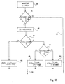
- Figure 2 is a simplified flowchart of a mode of implementation of a validation sequence for the presence of a transponder in the terminal field, applied to the state of standby of a read-write terminal.
- a transponder read-write terminal starts (block 20, ST), after an ignition, initialization and test phase, a watch procedure during which it waits for the establishment communication with a transponder.
- This procedure consists, essentially, of sending (block 21) periodically a interrogation sequence (REQ) for the transponder (s) possible in the terminal field.
- the reader monitors (block 22) the reception, by its receiver, of a response message (ACK) from a transponder entered in its field.
- the reader will loop on sending of a query 21.
- the reader When it receives an ACK response, it enters a verification mode that the transponder is correct a transponder intended for it, as well as in a mode possible anti-collision (block 23, INIT / COM) to individualize several transponders possibly present in the field.
- a verification mode that the transponder is correct a transponder intended for it, as well as in a mode possible anti-collision (block 23, INIT / COM) to individualize several transponders possibly present in the field.
- INIT / COM mode possible anti-collision
- the reader in response to a query request by a terminal, if several transponders are present in the field thereof, they can respond at the same time or with a time difference low enough to make the demodulation result by the unusable reader. This must then either select a transponder with which he wants to communicate, either assign different channels to different transponders.
- the terminal uses the results provided by its receiver.
- the values of these elements can also vary from a transponder to the other, provision is made according to the present invention to regulate the phase of the terminal's oscillating circuit with respect to a value reference.
- this phase regulation is performed by means of a loop whose response time is chosen so that the loop is slow enough so as not to hinder possible retromodulation from a transponder, and be fast enough before the speed of passage of a transponder in the terminal field.
- modulation frequencies by example, the frequency of the remote feed carrier of 13.56 MHz, and the retromodulation frequency of 847.5 kHz used in the data transmission from the transponder to the thick headed.
- phase control of the oscillating circuit of the terminal can be implemented using known means such as those described, for example, in the patent application European No. 0 857 981 already cited. Adaptation of the planned system by this document for the implementation of the invention, or of a another known phase control system, is within the range of the skilled person from the functional indications given in this description.
- the excitation voltage of the oscillating circuit is proportional by a coefficient constant at the voltage (VC1) across the capacitive element of terminal. Therefore, assess the apparent impedance of the circuit oscillating from the terminal amounts to assessing the relationship between the voltage across the capacitive element and the current in the oscillating circuit.
- the evaluation of the presence of a transponder carried out by the invention exclusively uses current information in the terminal oscillating circuit and voltage across the terminals this one, more precisely at the limits of its capacitive element (or information directly linked, by coefficients invariable and determined, at these magnitudes).
- the values known as "to empty ", current and voltage when no transponder is present in the terminal field are easily measurable on the read-write terminal side, for example, in a learning phase, for example, which follows the implementation of the terminal in its application site.
- Two embodiments of the invention corresponding to two corrective actions to undertake according to the type of demodulator of the read-write terminal.
- a first embodiment applied to a amplitude demodulation by the terminal will be described in relation with Figures 3A, 4A and 5A.
- FIG. 3A represents, schematically and simplified, a first embodiment of a read-write terminal according to the invention, equipped with a loop for regulating phase of the oscillating circuit and an amplitude demodulator.
- terminal 30 includes a circuit oscillating formed by an inductor or antenna L1, in series with a capacitive element 31 and a resistive element R1, between a terminal 32 output from an antenna amplifier or coupler 33 and a terminal 34 at a reference potential, (generally, ground).
- a measuring element 35 of the current in the oscillating circuit is interposed, for example, between the capacitive element 31 and the ground 34.
- This measurement element 35 is used, in particular, to deliver information of the current (I) intended for the operating means of the terminal side data, consisting for example of a microprocessor (not shown).
- the amplifier 33 receives a transmission signal E high frequency, from a modulator 36 (MOD1) which receives a reference frequency (OSC signal), for example, from a quartz oscillator (not shown).
- the modulator 36 receives, if necessary, a data signal Tx to be transmitted and, in the absence data transmission from the terminal, delivers the carrier high frequency (for example 13.56 MHz) suitable for remote supplying a transponder.
- the capacitive element 31 is a capacitive element variable and controllable by a CTRL signal.
- Phase regulation of the current is carried out in the antenna L1 with respect to a reference signal.
- This regulation is a high frequency signal regulation, that is to say of the carrier signal corresponding to signal E in the absence of data to be transmitted.
- This regulation is carried out in varying the capacity of the oscillating circuit of terminal 30 by so as to maintain the current in the antenna in phase relation constant with the reference signal which corresponds, for example, to the OSC signal supplied by the modulator oscillator.
- the regulation is slow enough not to take into account that the static phase variations in front of the subcarrier of retromodulation.
- the CTRL signal comes from a circuit 37 (COMP) whose role is to detect the phase deviation from the reference signal and modify the capacity accordingly of element 31.
- COMP circuit 37
- the phase measurement is made from a measurement of the current I in the circuit at by means of the current transformer 35 mounted in series with the element 31.
- This transformer generally consists of a primary winding 35 'between element 31 and earth, and of a secondary winding 35 "of which a first terminal is connected directly to earth 34 and a second terminal of which delivers a signal MES1 as a function of current I, sent to comparator 37 which consequently controls the capacitive element 31 by means of the signal CTRL.
- the signal MES1 is also sent, as previously indicated, to the microprocessor or analogous, to implement the validation method of the invention.
- a second measurement signal MES2 delivering a information on the voltage VC1 across the element capacitive 31, is also sent to the microprocessor. This signal is taken, for example, between the inductance L1 and the element 31.
- terminal 30 includes an amplitude demodulator 38 (DEMODA) receiving as input, for example, the voltage VC1 (or an image of the current) across the capacitive element 31 (more precisely, across the series association of this capacitive element 31 and intensity sensor 35), and outputting a signal Rx restoring a possible retromodulation of data received a transponder to the rest of the terminal's electronic circuits not shown.
- DEMODA amplitude demodulator 38
- FIG. 4A is a flow diagram of an implementation mode implementation of the validation method (block 24, FIG. 2) of the invention, applied to amplitude demodulation.
- the resistance R2 represents the equivalent resistance of all the circuits (micro
- the vacuum coefficient is zero insofar as the vacuum coupling is also zero.
- variable X2 is different from 0, i.e. its circuit oscillating is detuned even slightly. This is perfectly consistent with the fact that the transponder transmits data to destination of the terminal, i.e. it changes the charge that it constitutes on the terminal's oscillating circuit.
- the first case corresponds if no transponder is present in the field of the terminal.
- the correction made according to the invention to exit of a demodulation hole is preferably to force the value of the capacity C1 of the element 31 over a predetermined value during the learning phase.
- phase regulation is preferably carried out by a modification of the capacity of the oscillating circuit. Therefore, a variable capacitive element is provided for which the value, either to enslave the phase statically in the oscillating circuit, either to force the value of the capacitive element in order to shift the tuning of the circuit when we are in presence of a demodulation hole.
- the C1 capacity value is forced for example, by means of a COM signal delivered by the processor processing (not shown) to a circuit 39 for selecting the command to control element 31 between the CTRL signal delivered by circuit 37 and the forcing value.
- a COM signal delivered by the processor processing (not shown) to a circuit 39 for selecting the command to control element 31 between the CTRL signal delivered by circuit 37 and the forcing value.
- Practical realization of this function is within the reach of the skilled person.
- the phase regulator can be modified to be able to impose a different setpoint on it allowing the forced value of the capacity C1 is delivered by the signal CTRL.
- the capacity C1 of the element 31 of the oscillating circuit is forced (block 42) to a value C1 f equal to the empty value C1 that the latter had when empty.
- This value of the no-load capacity can easily be memorized in the learning phase where the no-load current and voltage have been measured.
- the initialization process ( Figure 2) continues (link 26) based on this new capacity value.
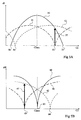
- FIG. 5A illustrates the first mode of implementation of the method of the invention by representing three examples of amplitudes variation of current I, available for the amplitude demodulator as a function of the C2 capacity of the transponder present in the terminal field. In other words, this illustrates the signal available to exploit a back modulation from a transponder using the demodulator amplitude.
- the variation of I corresponds, as a first approximation, the voltage variation dV across the element 31, and represents the signal to be detected by the amplitude demodulator 38. It is therefore a "dynamic" variation (at the rate of the retromodulation subcarrier, for example, 847.5 kHz).
- a first curve 50 drawn in solid lines corresponds to the ideal case where the imaginary part of the impedance X1 (formula 3) of the terminal's oscillating circuit is zero. This means that the terminal's oscillating circuit is perfectly tuned, including in its dynamic operation. This case is ideal insofar as the reader being provided with a phase loop, static with respect to the variations generated by the back modulation (for example, at 847 kHz), the apparent value X1 app is statically zero (formula 2). It will be remembered that the primary purpose of the static phase loop is to optimize the tuning as a function of the load of the transponder in order to obtain an optimal range of remote supply thereof.
- the shape 50 forms a kind of bell centered on the value C2 acc of the capacity of a transponder perfectly tuned on the remote supply carrier.
- the implementation of the correction provided by the invention corresponds to moving the operating point of the reader to the ideal curve (pace 50). This action is symbolized by a double arrow 57 at the point 53 taken as an example.
- the capacitive element 31 of variable capacity consists of a diode or a transistor, the junction capacity of which is varied by modifying the voltage applied to its terminals, it can be considered that this voltage control corresponds to the voltage VC1.
- this voltage control corresponds to the voltage VC1.
- it is possible to store, in a learning phase, only the value of the no-load capacity as well as the no-load current. Then, as soon as a demodulation hole is detected, the element C1 is polarized to an empty value VC1 which is calculated by the following formula: VC1 empty I empty ⁇ C1 empty .
- FIGS. 3B, 4B and 5B A second embodiment of the invention applied to a phase demodulation by the terminal will be described below in relationship with FIGS. 3B, 4B and 5B which are to be compared with Figures 3A, 4A and 5A which have just been described.
- FIG. 3B represents an embodiment of a terminal 30 according to the present invention applied to demodulation phase with it.
- the difference between the terminal of the figure 3B and that of FIG. 3A is mainly linked to the demodulator used.
- a demodulator of phase (DEMODP) delivers the Rx signal from demodulated data to from an assessment of the phase shift at the rate of the retromodulation emitted by a transponder.
- the comparator 37 of the phase control loop uses the same phase detector than the one used to demodulate the signal from the transponder. Consequently, the signal Rx is delivered by the comparator 37. It will be remembered, however, that the interpretation of the result detection is different.
- the receiver takes into account dynamic variations (at the frequency of the subcarrier) while that the phase regulator takes account of static variations.
- the phase regulator takes account of static variations.
- two phase detectors separate.
- the rest of terminal 30 is similar to the constitution exposed in relation to FIG. 3A applied to the amplitude demodulation.
- FIG. 4B illustrates, by a flowchart, the correction applied according to the invention to the value of the element terminal capacitive in the presence of a demodulation hole of phase.
- Blocks 40 and 41 are similar to those exposed in relationship to Figure 4A.
- force the value of capacity C1 to its value at vacuum would amount to forcing the tuning of the oscillating circuit of the terminal on the carrier frequency.
- FIG. 5B represents three examples of appearance of variation d ⁇ of the phase in the oscillating circuit of the terminal in function of the value taken by the capacity C2 of the circuit oscillating from the transponder.
- Figure 5B is close to the FIG. 5A applied to the amplitude modulation.
- a first curve 60 drawn in solid lines corresponds in the ideal case where the imaginary part of the impedance X1 (formula 3) the oscillating circuit of the terminal is zero. Like before, this corresponds to the ideal case of a perfect chord of the thick headed.
- the pace 60 increases in a hyperbolic fashion, symmetrically on either side of a minimum 65 at the value C2 acc of the capacity of a transponder perfectly tuned on the remote supply carrier and which, in phase demodulation, corresponds to a demodulation hole.
- the zero crossing 65 of the curve 60 representing the ideal case corresponds to a capacity value C2 included in tolerance and drift ranges.
- the invention proposes a new analysis of the behavior of the oscillating circuits of a terminal and a transponder to determine, always from calculated values in a learning phase and a comparison by compared to current values, the correction to be made.
- the invention plans to force a value of X1 of opposite sign and large enough to deviate from the "theoretical" or “ideal” agreement 65. This amounts to passing on another curve of which not only the minimum is separated from the current minimum through point 65, but whose impedance value apparent is also different. So we have to accept here a reduction in the remote supply of the transponder. We seeks, however, to ensure that this drop is minimal.
- a force value C1 f must be provided which can be easily determined by calculation from stored and measured values.
- X1 we can force the value of k to k max to put in the same conditions as those of a transponder with maximum coupling where we know that we are out of a demodulation hole
- the coefficient k max is, approximately but sufficiently, known for a given family of transponders for which the terminal in question is intended. It is generally between approximately 0.1 and 0.4.
- the dynamic phase shift d ⁇ can be measured, either on current I, or on voltage VC1 or similar. Consequently, the invention also applies to the case where other means than an intensity sensor are used to detect the phase shift. It depends on the type of receiver phase used.
- FIG. 6 represents, schematically and simplified, a third embodiment of the present invention applied to a read-write terminal 70 provided, for the demodulation of the signals coming from a retromodulation by a transponder, both of a phase demodulator (DEMODP) and an amplitude demodulator (DEMODA).
- DEMODP phase demodulator
- DEMODA amplitude demodulator
- the interpretation of the existence of a transponder in the terminal field is then used, not to modify the capacity of the variable element of the terminal's oscillating circuit, but to select the demodulator to use to extract the signal Rx .
- the demodulation holes do not have the same positions (in terms of the capacitance C2) depending on whether the terminal demodulates in amplitude or in phase.
- the demodulator of the opposite type is not "blind” insofar as the change of demodulator does not modify the imaginary part X1 app of the apparent impedance.
- changing the demodulator when one is in a hole, for example 53 or 54 amounts to placing oneself on the curve 61, respectively 62, for the same capacity value C2.
- Terminal 70 includes the same elements as those common to terminals 30 of Figures 3A and 3B with the exception of circuit 39. It further comprises an amplitude demodulator 38 connected as in Figure 3A and a phase demodulator, preferably similar to that of Figure 3B.
- a circuit 71 of selection receives the respective outputs 72 and 73 from the demodulators amplitude and phase and delivers the signal Rx to destination of the processing processor (not shown).
- the circuit 71 is controlled by a two-state COM signal from the processing processor and obtained, preferably, in a way similar to that of the embodiments described above.
- a priority demodulator that is to say selected, is determined in the absence of a demodulation hole.
- An advantage of the present invention is that by means of determination of easily measurable electrical quantities, the reliability of the operation of a electromagnetic transponder read-write terminal.
- Another advantage of the invention is that one intervenes than on the read-write terminal side. Therefore, the operation of the transponder present in the terminal field is not affected and the invention can be implemented with existing conventional transponders.
- Another advantage of the invention is that by choosing to intervene on the variable of adjustment of the static loop of phase regulation, structural modifications are minimized of the terminal.
- Another advantage of the present invention is that it makes the transponder system function insensitive to demodulation holes.
- Another advantage of the present invention is that the correction implemented does not harm the remote supply of the transponder.
- Another advantage of the present invention is that it does not require any adaptation according to the sensitivity of the demodulator. We can even consider that it adapts automatically to a variation of the demodulation threshold. Indeed, as the correction made by the invention is implemented from of the demodulation result, it is independent of the threshold of detection of the demodulator.
- the invention transposes in the case of a "capacitive" retromodulation which modifies the value of the capacitance C2 to the rhythm of the subcarrier.
- the holes demodulation are functions of resistance R2 and therefore vary depending on the consumption of the transponder circuits.
- the the detection principle described above is not changed in any way. We will simply adapt the correction on the terminal side.
Landscapes
- Engineering & Computer Science (AREA)
- Artificial Intelligence (AREA)
- Computer Vision & Pattern Recognition (AREA)
- Physics & Mathematics (AREA)
- General Physics & Mathematics (AREA)
- Theoretical Computer Science (AREA)
- Near-Field Transmission Systems (AREA)
- Radar Systems Or Details Thereof (AREA)
Abstract
L'invention concerne un procédé de commande d'une borne de génération d'un champ électromagnétique au moyen d'un signal d'excitation d'un circuit oscillant, pourvue de moyens de régulation de la phase du signal dans le circuit oscillant, consistant à comparer des valeurs courantes de grandeurs liées au courant dans le circuit oscillant et à la tension à ses bornes par rapport à des valeurs prédéterminées, afin de détecter (24) la présence d'un transpondeur dans le champ électromagnétique. <IMAGE>The invention relates to a method for controlling a terminal for generating an electromagnetic field by means of an excitation signal of an oscillating circuit, provided with means for regulating the phase of the signal in the oscillating circuit, comprising comparing current values of quantities linked to the current in the oscillating circuit and to the voltage at its terminals with respect to predetermined values, in order to detect (24) the presence of a transponder in the electromagnetic field. <IMAGE>
Description
La présente invention concerne des systèmes utilisant des transpondeurs électromagnétiques, c'est-à-dire des émetteurs-récepteurs (généralement mobiles) susceptibles d'être interrogés, sans contact et sans fil, par une unité (généralement fixe) dite borne de lecture et/ou d'écriture. Généralement, les transpondeurs extraient l'alimentation nécessaire aux circuits électroniques qu'ils comportent d'un champ haute fréquence rayonné par une antenne de la borne de lecture et d'écriture.The present invention relates to systems using electromagnetic transponders, i.e. transceivers (generally mobile) likely to be questioned, contactless and wireless, by a so-called (generally fixed) unit reading and / or writing terminal. Generally, transponders extract the power necessary for the circuits electronic they have a high frequency field radiated by an antenna from the read and write terminal.
La figure 1 représente, de façon très schématique et simplifiée, un exemple classique de système d'échange de données du type auquel se rapporte la présente invention entre une borne 1 de lecture-écriture et un transpondeur 10.FIG. 1 very schematically represents and simplified, a classic example of a data exchange system of the type to which the present invention relates between a terminal 1 read-write and a transponder 10.
Généralement, la borne 1 est essentiellement constituée d'un circuit oscillant série, formé d'une inductance L1 en série avec un condensateur C1 et une résistance R1, entre une borne 2 de sortie d'un amplificateur ou coupleur d'antenne 3 et une borne 4 à un potentiel de référence (généralement, la masse). L'amplificateur 3 reçoit un signal E de transmission haute fréquence, issu d'un modulateur 5 (MOD1) qui reçoit une fréquence de référence (signal OSC) par exemple, d'un oscillateur à quartz (non représenté). Le modulateur 5 reçoit, si besoin, un signal Tx de données à transmettre et, en l'absence de transmission de données depuis la borne, délivre la porteuse haute fréquence (par exemple, 13,56 MHz) propre à téléalimenter un transpondeur. En réception, la borne 1 utilise un démodulateur 6 (DEMOD1) qui sert à détecter une variation de charge engendrée par le transpondeur 10 sur le signal haute fréquence. Le démodulateur 6 prélève, par exemple, la tension aux bornes 7 et 4 du condensateur C1, et délivre un signal Rx de données reçues après démodulation.Generally, terminal 1 is essentially made up of a series oscillating circuit, formed of an inductance L1 in series with a capacitor C1 and a resistor R1, between a terminal 2 output of an antenna amplifier or coupler 3 and a terminal 4 to a reference potential (generally, the mass). The amplifier 3 receives a high frequency transmission signal E, from a modulator 5 (MOD1) which receives a reference frequency (OSC signal) for example, a quartz oscillator (not represented). The modulator 5 receives, if necessary, a signal Tx of data to be transmitted and, in the absence of data transmission from the terminal, delivers the high frequency carrier (for example, 13.56 MHz) suitable for remote powering a transponder. In reception, terminal 1 uses a demodulator 6 (DEMOD1) which is used to detect a load variation generated by the transponder 10 on the high frequency signal. The demodulator 6 takes, for example, the voltage at terminals 7 and 4 of capacitor C1, and delivers a Rx signal of data received after demodulation.
D'autres circuits non représentés équipent généralement une borne 1. Parmi ces circuits, on retrouve, entre autres et de façon non limitative, un circuit de commande et d'exploitation des données reçues basé, le plus souvent, sur un microprocesseur de traitement des commandes et des données. Ces circuits communiquent généralement avec différents circuits d'entrée/sortie (clavier, écran, moyen d'échange avec un serveur, etc.) et/ou de traitement non représenté. Les circuits de la borne de lecture-écriture tirent l'énergie nécessaire à leur fonctionnement d'un circuit d'alimentation (non représenté) raccordé, par exemple, au réseau de distribution électrique ou à des batteries.Other circuits not shown generally equip A terminal 1. Among these circuits, we find, among others and without limitation, a control and operating circuit data received based, more often than not, on a microprocessor processing orders and data. These circuits communicate usually with different input / output circuits (keyboard, screen, means of exchange with a server, etc.) and / or processing not shown. Read-write terminal circuits draw the energy necessary for their operation from a supply circuit (not shown) connected, for example, to the electrical distribution network or batteries.
Un transpondeur 10, destiné à coopérer avec une borne 1, comporte essentiellement un circuit oscillant parallèle formé d'une inductance L2 en parallèle avec un condensateur C2 entre deux bornes 11 et 12 d'entrée d'un circuit 13 de commande et de traitement. Les bornes 11 et 12 sont, en pratique, reliées à l'entrée d'un moyen de redressement (non représenté) dont des sorties constituent des bornes d'alimentation continue des circuits internes au transpondeur. Ces circuits comprennent généralement, essentiellement, un microprocesseur 14 (P) susceptible de communiquer avec d'autres éléments (par exemple, une mémoire) par des liaisons 15. Le transpondeur 10 comprend en outre un démodulateur 16 (DEMOD2) des signaux reçus de la borne 1 qui délivre un signal Rx' au circuit 14, et un modulateur 17 (MOD2) pour transmettre, à la borne, des informations Tx' qu'il reçoit du circuit 14.A transponder 10, intended to cooperate with a terminal 1, essentially comprises a parallel oscillating circuit formed inductance L2 in parallel with a capacitor C2 between two input terminals 11 and 12 of a circuit 13 for controlling and treatment. Terminals 11 and 12 are, in practice, connected to the entry of a rectifying means (not shown) including outputs constitute DC power supply terminals internal to the transponder. These circuits generally include, essentially, a microprocessor 14 (P) capable of communicating with other elements (for example, a memory) by connections 15. The transponder 10 further comprises a demodulator 16 (DEMOD2) signals received from terminal 1 which delivers a signal Rx 'at circuit 14, and a modulator 17 (MOD2) for transmitting, to the terminal, information Tx 'which it receives from circuit 14.
Les circuits oscillants de la borne et du transpondeur sont généralement accordés sur une même fréquence correspondant à la fréquence d'un signal d'excitation du circuit oscillant de la borne. Ce signal haute fréquence (par exemple 13,56 MHz) sert non seulement de porteuse de transmission mais également de porteuse de téléalimentation à destination du ou des transpondeurs se trouvant dans le champ de la borne. Quand un transpondeur 10 se trouve dans le champ d'une borne 1, une tension haute fréquence est engendrée aux bornes 11 et 12 de son circuit résonnant. Cette tension, après redressement et écrêtement éventuel, est destinée à fournir la tension d'alimentation des circuits électroniques 13 du transpondeur. Pour des raisons de clarté, les moyens de redressement, d'écrêtement et de fourniture d'alimentation n'ont pas été représentés en figure 1. On notera que, généralement, la démodulation (bloc 16) s'effectue en amont des moyens d'écrêtement pour préserver la modulation des données en amplitude sur la porteuse haute fréquence émise par la borne. Cette modulation d'amplitude s'effectue selon différentes techniques de codage afin de transmettre des données et/ou des commandes aux transpondeurs. En retour, la transmission de données Tx' du transpondeur vers une borne s'effectue généralement en modulant la charge constituée par le circuit résonnant L2, C2. C'est pourquoi le modulateur 17 a été représenté en parallèle sur ce circuit résonnant. La variation de charge s'effectue au rythme d'une sous porteuse, dite de rétromodulation, de fréquence (par exemple 847,5 kHz) inférieure à celle de la porteuse.Oscillating circuits of the terminal and the transponder are generally tuned on the same frequency corresponding to the frequency of an excitation signal of the oscillating circuit of the thick headed. This high frequency signal (for example 13.56 MHz) is used only transmission carrier but also carrier remote power supply to the transponder (s) found in the terminal field. When a 10 transponder finds in the field of a terminal 1, a high frequency voltage is generated at terminals 11 and 12 of its resonant circuit. This tension, after rectification and possible capping, is intended to supply the supply voltage of the electronic circuits 13 of the transponder. For reasons of clarity, the means of straightening, capping, and supplying power not shown in Figure 1. Note that, generally, the demodulation (block 16) takes place upstream of the clipping means to preserve the modulation of the amplitude data on the high frequency carrier transmitted by the terminal. This modulation amplitude is performed using different coding techniques in order to transmit data and / or commands to the transponders. In return, the Tx 'data transmission from the transponder towards a terminal is generally carried out by modulating the load constituted by the resonant circuit L2, C2. This is why the modulator 17 has been shown in parallel on this resonant circuit. The charge variation is carried out at the rate of a sub carrier, called retromodulation, of frequency (for example 847.5 kHz) lower than that of the carrier.
La variation de charge provenant d'un transpondeur peut alors être détectée par la borne sous la forme d'une variation d'amplitude ou d'une variation de phase au moyen, par exemple, d'une mesure de la tension aux bornes du condensateur C1 ou du courant dans le circuit oscillant à l'aide du démodulateur 6.The load variation from a transponder can then be detected by the terminal as a variation amplitude or phase variation using, for example, a measurement of the voltage across the capacitor C1 or the current in the oscillating circuit using the demodulator 6.
Un problème qui se pose dans les systèmes à transpondeur électromagnétique classiques est qu'il arrive qu'un transpondeur téléalimenté par une borne et émettant des données à destination de celle-ci ne soit pas détecté par la borne, c'est-à-dire que le démodulateur de la borne ne parvienne pas à détecter la présence d'une modulation de données. Ce phénomène est généralement désigné par l'expression "trou de démodulation". Pour un système donné, il s'agit d'une position relative d'une borne et d'un transpondeur à laquelle le démodulateur de la borne est "aveugle".A problem that arises in transponder systems classic electromagnetic is that sometimes a transponder remotely powered by a terminal and transmitting data to destination of it is not detected by the terminal, that is to say the terminal demodulator does not reach detect the presence of data modulation. This phenomenon is generally referred to as the "demodulation hole". For a given system, it is a relative position of a terminal and a transponder to which the terminal demodulator is "blind".
On notera que cette notion de trou de démodulation est différente de ce que l'on désigne par "trou de téléalimentation" où c'est le transpondeur qui ne parvient pas à être alimenté par le signal haute fréquence alors même qu'il est dans le champ électromagnétique de la borne. En effet, il existe une position relative entre un transpondeur et une borne à laquelle le couplage magnétique entre les circuits oscillants est tel que le transpondeur n'est pas alimenté, c'est-à-dire que la tension récupérée aux bornes 11 et 12 de son circuit oscillant est trop faible pour qu'il fonctionne. Dans un trou de démodulation, le transpondeur est correctement alimenté. Il détecte généralement correctement les données transmises par la borne en modulation d'amplitude. Il émet correctement des données à la borne en rétromodulation, par variation de la charge de son circuit oscillant. Toutefois, le démodulateur de la borne ne détecte pas cette rétromodulation.Note that this notion of demodulation hole is different from what we call "remote feeding hole" where it is the transponder which fails to be powered by the high frequency signal even while it is in the field electromagnetic terminal. Indeed, there is a position relative between a transponder and a terminal to which coupling magnetic between the oscillating circuits is such that the transponder is not supplied, i.e. the voltage recovered at terminals 11 and 12 of its oscillating circuit is too weak for it to work. In a demodulation hole, the transponder is correctly supplied. It generally detects correctly the data transmitted by the terminal in modulation amplitude. It correctly transmits data to the terminal in retromodulation, by variation of the load of its circuit oscillating. However, the terminal's demodulator does not detect this retromodulation.
Ce problème de trou de démodulation fait qu'une borne peut ne pas détecter un transpondeur présent dans son champ dans la mesure où cette détection fait classiquement appel au résultat du démodulateur de données côté borne. En particulier, lorsqu'elle est dans un état de veille en attente d'une transmission, une borne émet périodiquement des requêtes d'interrogation en modulant l'amplitude de la porteuse de téléalimentation. La borne surveille alors la sortie de son démodulateur qui lui indiquera la présence d'un transpondeur. En effet, quand un transpondeur se trouve "réveillé" par son entrée dans le champ d'une borne, celui-ci démodule le message d'interrogation transmis périodiquement par cette borne et y répond pour se faire identifier.This demodulation hole problem causes a terminal may not detect a transponder present in its field in the extent to which this detection conventionally uses the result of the terminal side data demodulator. In particular, when is in a standby state awaiting transmission, a terminal periodically issues interrogation requests in modulating the amplitude of the remote power carrier. Terminal then monitors the output of its receiver which will tell it the presence of a transponder. Indeed, when a transponder is finds "awakened" by its entry in the field of a terminal, this demodulates the interrogation message transmitted periodically by this terminal and responds to it to be identified.
Un inconvénient supplémentaire est que, comme le transpondeur a de son côté reçu des données de la borne, celui-ci se croít identifié par la borne ce qui n'est pas vrai. Les seules techniques actuelles pour isoler ce phénomène sont de multiplier les échanges d'informations pour valider la transmission, ce qui est coûteux en terme de durée de transmission.An additional disadvantage is that, like the transponder for its part received data from the terminal, it believes identified by the terminal which is not true. The only ones current techniques to isolate this phenomenon are to multiply exchanges of information to validate the transmission, which is expensive in terms of transmission time.
Différents systèmes à transpondeur du type auquel s'applique la présente invention sont décrits, par exemple, dans les brevets américains n° 4 963 887 et 5 550 536, ainsi que dans les demandes de brevets européens n° 0 722 094 et 0 857 981.Different transponder systems of the type to which applies the present invention are described, for example, in U.S. Patents 4,963,887 and 5,550,536, as well as in European patent applications Nos. 0 722 094 and 0 857 981.
Dans une borne de lecture/écriture pourvue d'un démodulateur d'amplitude, la tension de sortie du démodulateur s'annule, c'est-à-dire que l'on est en présence d'un trou de démodulation dans deux configurations de fréquence de la porteuse (13,56 MHz) qui, pour un coefficient de couplage donné entre les circuits oscillants de la borne et du transpondeur concerné, encadrent la fréquence de résonance propre du circuit oscillant L2-C2 du transpondeur. De manière idéale, cette fréquence médiane correspond à l'accord parfait de la borne et du transpondeur sur la fréquence de la porteuse de téléalimentation, où l'amplitude disponible pour la démodulation est maximale.In a read / write terminal provided with a demodulator amplitude, the output voltage of the demodulator is canceled, that is to say that one is in the presence of a hole of demodulation in two carrier frequency configurations (13.56 MHz) which, for a given coupling coefficient between the oscillating circuits of the terminal and the transponder concerned, frame the resonant frequency of the oscillating circuit L2-C2 of the transponder. Ideally, this median frequency corresponds to the perfect match between the terminal and the transponder on the frequency of the remote feed carrier, where the amplitude available for demodulation is maximum.
On cherche généralement à ce que les circuits oscillants de la borne et du transpondeur soient tous deux accordés sur la fréquence de la porteuse de téléalimentation de façon à maximiser l'énergie de téléalimentation reçue par le transpondeur. Toutefois, les tolérances de fabrication des condensateurs utilisés pour les circuits oscillants, en particulier pour le condensateur C2 du transpondeur qui est généralement intégré, sont généralement de l'ordre de 10 %. L'importance de ces tolérances de fabrication conduit à ce que l'accord parfait n'est pratiquement pas respecté et que l'on ne peut garantir qu'un transpondeur entrant dans le champ d'une borne ne se trouvera pas, dans une position de couplage donnée, dans un trou de démodulation.We generally try to ensure that the circuits of the terminal and the transponder are both tuned to the frequency of the remote power carrier so as to maximize the remote power energy received by the transponder. However, the manufacturing tolerances of capacitors used for oscillating circuits, in particular for the capacitor C2 of the transponder which is generally integrated, are generally around 10%. The importance of these manufacturing tolerances means that the perfect agreement is practically not respected and that one does not can guarantee that a transponder falling within the scope of a terminal will not be in a given coupling position, in a demodulation hole.
De plus, la position des trous de démodulation dans la réponse du démodulateur d'amplitude varie en fonction de la mutuelle inductance entre les circuits oscillants. Or, cette mutuelle inductance dépend de la distance qui sépare les antennes L1 et L2 de la borne et du transpondeur, donc de la position relative du transpondeur par rapport à la borne lors de la transmission.In addition, the position of the demodulation holes in the amplitude demodulator response varies depending on the mutual inductance between the oscillating circuits. Now, this mutual inductance depends on the distance between the antennas L1 and L2 of the terminal and the transponder, therefore of the position relative of the transponder to the terminal during transmission.
Dans une borne de lecture/écriture pourvue d'un démodulateur de phase, la tension de sortie du démodulateur s'annule, c'est-à-dire que l'on est en présence d'un trou de démodulation dans une configuration de fréquence qui, pour un coefficient de couplage donné entre les circuits oscillants de la borne et du transpondeur concerné, correspond à l'accord parfait de la borne et du transpondeur sur la fréquence de la porteuse de téléalimentation. Côté transpondeur, cette fréquence est alors la fréquence de résonance propre du circuit oscillant L2-C2 du transpondeur.In a read / write terminal provided with a demodulator phase, the output voltage of the demodulator is canceled, that is to say that we are in the presence of a demodulation hole in a frequency configuration which, for a coefficient of given coupling between the oscillating circuits of the terminal and the transponder concerned, corresponds to the perfect match of the terminal and the transponder on the frequency of the remote feed carrier. Transponder side, this frequency is then the frequency resonance of the L2-C2 oscillating circuit of the transponder.
On a déjà proposé de désaccorder à demeure les circuits oscillants de la borne et du transpondeur de façon à ce que ces deux circuits ne soient pas tous deux accordés sur la fréquence de la porteuse de téléalimentation. Toutefois, un inconvénient qui en découle est que cela nuit à la téléalimentation du transpondeur, et donc à la portée du système.We have already proposed to permanently detune the circuits oscillating of the terminal and the transponder so that these two circuits are not both tuned on frequency of the remote power carrier. However, a downside which results from this is that it harms the remote supply of the transponder, and therefore within the reach of the system.
De plus, l'importance des tolérances de fabrication des condensateurs conduit à devoir se décaler sensiblement de la fréquence de la porteuse si l'on veut diminuer les risques de trous de démodulation.In addition, the importance of manufacturing tolerances for capacitors leads to having to shift significantly from the carrier frequency if we want to reduce the risk of demodulation holes.
Ainsi, un inconvénient notable des systèmes classiques à démodulation de phase, est que l'on est contraint d'effectuer un compromis entre la téléalimentation et la capacité de démodulation de phase par la borne. De plus, ce compromis est délicat à réaliser, la position du trou dans la réponse du démodulateur de phase variant en fonction de la mutuelle inductance entre les circuits oscillants.Thus, a notable drawback of conventional systems phase demodulation, is that we are forced to perform a compromise between remote power supply and demodulation capacity phase through the terminal. In addition, this compromise is delicate to realize, the position of the hole in the response of the demodulator of phase varying according to the mutual inductance between the oscillating circuits.
Les problèmes combinés d'existence de trous de démodulation, et de la variation de la position de ces trous de démodulation par rapport à la distance entre les inductances, associés aux tolérances de fabrication des composants, rendent les systèmes classiques peu fiables. The combined problems of existence of demodulation holes, and the variation in the position of these holes demodulation with respect to the distance between the inductors, associated with the manufacturing tolerances of the components, make unreliable conventional systems.
La présente invention vise à pallier les inconvénients des systèmes classiques relatifs à la présence de trous de démodulation dans la réponse du démodulateur d'une borne de lecture-écriture.The present invention aims to overcome the drawbacks conventional systems relating to the presence of demodulation holes in the response of the demodulator of a read-write terminal.
Plus particulièrement, la présente invention vise à proposer un nouveau procédé de commande qui rende une borne de lecture-écriture insensible aux trous de démodulation des données qu'elle reçoit d'un transpondeur entré dans son champ.More particularly, the present invention aims to propose a new control method which makes a terminal read-write insensitive to data demodulation holes that it receives from a transponder entered in its field.
La présente invention vise également à proposer une nouvelle borne insensible aux trous de démodulation des données qu'elle reçoit d'un transpondeur entré dans son champ.The present invention also aims to provide a new terminal insensitive to data demodulation holes that it receives from a transponder entered in its field.
La présente invention vise également à proposer une solution n'entraínant aucune modification des transpondeurs et qui soit par conséquent compatible avec les transpondeurs existants.The present invention also aims to provide a solution resulting in no modification of the transponders and which is therefore compatible with existing transponders.
Pour atteindre ces objets, la présente invention prévoit un procédé de commande d'une borne de génération d'un champ électromagnétique au moyen d'un signal d'excitation d'un circuit oscillant, pourvue de moyens de régulation de la phase du signal dans le circuit oscillant, consistant à comparer des valeurs courantes de grandeurs liées au courant dans le circuit oscillant et à la tension à ses bornes par rapport à des valeurs prédéterminées, afin de détecter la présence d'un transpondeur dans le champ électromagnétique.To achieve these objects, the present invention provides a method for controlling a generation terminal of a field electromagnetic by means of a circuit excitation signal oscillating, provided with means for regulating the signal phase in the oscillating circuit, consisting in comparing values currents of quantities linked to the current in the oscillating circuit and the voltage across its terminals with respect to predetermined values, in order to detect the presence of a transponder in the electromagnetic field.
Selon un mode de réalisation de la présente invention, lesdites valeurs prédéterminées sont mesurées et mémorisées lors d'un fonctionnement à vide de la borne, alors qu'aucun transpondeur n'est présent dans son champ.According to an embodiment of the present invention, said predetermined values are measured and stored during no-load operation of the terminal, while no transponder is not present in its field.
Selon un mode de réalisation de la présente invention, ladite détection de présence est mise en oeuvre quand un démodulateur que comporte la borne ne détecte aucun signal émis par un transpondeur.According to an embodiment of the present invention, said presence detection is implemented when a demodulator that the terminal has does not detect any signal emitted by a transponder.
Selon un mode de réalisation de la présente invention, le procédé consiste, en cas de présence détectée d'un transpondeur, à désactiver la régulation de phase, et à forcer la partie imaginaire de l'impédance du circuit oscillant de la borne à une valeur prédéterminée.According to an embodiment of the present invention, the method consists, in the presence of a transponder detected, to deactivate the phase regulation, and to force the part imaginary of the impedance of the oscillating circuit from the terminal to a predetermined value.
Selon un mode de réalisation de la présente invention, le forçage de ladite partie imaginaire est effectué en forçant la valeur d'un élément capacitif variable du circuit oscillant.According to an embodiment of the present invention, the forcing of said imaginary part is carried out by forcing the value of a variable capacitive element of the oscillating circuit.
Selon un mode de réalisation de la présente invention, appliqué à une borne pourvue d'un démodulateur d'amplitude, la valeur prédéterminée de forçage de ladite partie imaginaire correspond à un fonctionnement à vide de la borne.According to an embodiment of the present invention, applied to a terminal provided with an amplitude demodulator, the predetermined forcing value of said imaginary part corresponds to an empty operation of the terminal.
Selon un mode de réalisation de la présente invention, appliqué à une borne pourvue d'un démodulateur de phase, la valeur prédéterminée de forçage de ladite partie imaginaire est fonction de la position de cette partie imaginaire par rapport à une valeur limite correspondant à un fonctionnement à vide de la borne.According to an embodiment of the present invention, applied to a terminal provided with a phase demodulator, the predetermined forcing value of said imaginary part is function of the position of this imaginary part with respect to a limit value corresponding to an idle operation of the thick headed.
Selon un mode de réalisation de la présente invention, le procédé consiste, en cas de présence détectée d'un transpondeur et en cas d'absence de détection de données par un démodulateur actif parmi un démodulateur d'amplitude et un démodulateur de phase que comporte la borne, à sélectionner l'autre démodulateur pour détecter les données.According to an embodiment of the present invention, the method consists, in the presence of a transponder detected and in the absence of data detection by a active demodulator among an amplitude demodulator and a demodulator phase of the terminal, select the other demodulator to detect data.
La présente invention prévoit également une borne de génération d'un champ électromagnétique propre à coopérer avec au moins un transpondeur lorsque ce dernier entre dans ce champ, et comportant des moyens pour mettre en oeuvre le procédé de l'invention.The present invention also provides a terminal generation of an electromagnetic field suitable for cooperating with minus a transponder when the latter enters this field, and comprising means for implementing the method of the invention.
Ces objets, caractéristiques et avantages, ainsi que
d'autres de la présente invention seront exposés en détail dans
la description suivante de modes de réalisation particuliers
faite à titre non-limitatif en relation avec les figures jointes
parmi lesquelles :
Les mêmes éléments ont été désignés par les mêmes références aux différentes figures. Pour des raisons de clarté, seuls les éléments d'une borne et d'un transpondeur et seules les étapes de procédé d'échange d'informations qui sont nécessaires à la compréhension de l'invention ont été illustrés aux figures et seront décrits par la suite. En particulier, les détails constitutifs des modulateurs et démodulateurs n'ont pas été détaillés et sont à la portée de l'homme du métier à partir des indications fonctionnelles données ci-après. En outre, l'invention sera exposée en relation avec des transpondeurs utilisant une rétromodulation dite "résistive" pour faire varier la charge qu'ils constituent sur le circuit oscillant de la borne (les capacités des circuits oscillants des transpondeurs étant fixes), mais on notera que l'invention s'applique plus généralement à tout type de rétromodulation, par exemple à une rétromodulation dite "capacitive".The same elements have been designated by the same references to the different figures. For reasons of clarity, only the elements of a terminal and a transponder and only the steps in the information exchange process that are necessary to the understanding of the invention have been illustrated in the figures and will be described later. In particular, the constituent details modulators and demodulators have not been detailed and are within the reach of the skilled person from the indications functional data given below. In addition, the invention will exposed in relation to transponders using retromodulation called "resistive" to vary the charge they constitute on the oscillating circuit of the terminal (the capacities oscillating circuits of the transponders being fixed), but note that the invention more generally applies to any type retromodulation, for example a so-called retromodulation "capacitive".
Une caractéristique de la présente invention est de prévoir une détermination directe de la présence d'un transpondeur dans le champ d'une borne de lecture-écriture, c'est-à-dire sans qu'il soit nécessaire d'interpréter des signaux démodulés de transmission de données émanant de ce transpondeur. Plus précisément, la présente invention prévoit, en cas d'absence d'un signal démodulé utilisable par la borne, de valider l'absence d'un transpondeur dans le champ de celle-ci par une autre détermination indépendante de l'existence d'une transmission de données.A feature of the present invention is provide for direct determination of the presence of a transponder in the field of a read-write terminal, i.e. without the need to interpret demodulated signals from transmission of data from this transponder. More precisely, the present invention provides, in the absence of a signal demodulated usable by the terminal, to validate the absence of a transponder within the scope thereof by another determination independent of the existence of data transmission.
Une autre caractéristique de la présente invention est de prévoir, en cas d'incohérence entre le résultat du démodulateur et de la détermination directe, une action correctrice permettant au démodulateur de la borne d'interpréter correctement les données reçues. Cette action correctrice s'effectue préférentiellement sur le circuit oscillant de la borne et, de préférence, sur l'élément capacitif de ce circuit.Another feature of the present invention is to provide, in case of inconsistency between the result of the receiver and direct determination, corrective action allowing the terminal demodulator to interpret correctly the data received. This corrective action is preferably carried out on the terminal's oscillating circuit and, from preferably on the capacitive element of this circuit.
La détermination de la présence ou de l'absence d'un transpondeur dans le champ de la borne s'effectue, selon l'invention, par une mesure du courant dans le circuit oscillant de la borne et de la tension aux bornes de son élément capacitif (ou de grandeurs directement liées au courant et à la tension), et en comparant les valeurs courantes obtenues à des valeurs mémorisées précédemment. Ces dernières correspondent, de préférence, à des valeurs mesurées dans une phase d'apprentissage où le lecteur est dans une configuration particulière. The determination of the presence or absence of a transponder in the terminal field is carried out, according to the invention, by measuring the current in the oscillating circuit of the terminal and the voltage across its capacitive element (or quantities directly related to current and voltage), and comparing the current values obtained with stored values previously. The latter preferably correspond to values measured in a learning phase where the reader is in a particular configuration.
Par la suite, l'action correctrice éventuelle peut faire appel à différents calculs et comparaisons, notamment, en fonction du type de démodulation (phase ou amplitude) utilisé par la borne.Thereafter, possible corrective action may use different calculations and comparisons, in particular, by depending on the type of demodulation (phase or amplitude) used by terminal.
La figure 2 est un organigramme simplifié d'un mode de mise en oeuvre d'une séquence de validation de la présence d'un transpondeur dans le champ de la borne, appliqué à l'état de veille d'une borne de lecture-écriture.Figure 2 is a simplified flowchart of a mode of implementation of a validation sequence for the presence of a transponder in the terminal field, applied to the state of standby of a read-write terminal.
Dès qu'elle est mise sous tension et en fonctionnement, une borne de lecture-écriture de transpondeur débute (bloc 20, ST), après une phase d'allumage, d'initialisation et de test, une procédure de veille pendant laquelle elle attend l'établissement d'une communication avec un transpondeur. Cette procédure consiste, essentiellement, à envoyer (bloc 21) périodiquement une séquence d'interrogation (REQ) à destination du ou des transpondeurs éventuels présents dans le champ de la borne. Après chaque envoi de requête d'interrogation 21, le lecteur surveille (bloc 22) la réception, par son démodulateur, d'un message de réponse (ACK) provenant d'un transpondeur entré dans son champ.As soon as it is powered up and in operation, a transponder read-write terminal starts (block 20, ST), after an ignition, initialization and test phase, a watch procedure during which it waits for the establishment communication with a transponder. This procedure consists, essentially, of sending (block 21) periodically a interrogation sequence (REQ) for the transponder (s) possible in the terminal field. After each sending of interrogation request 21, the reader monitors (block 22) the reception, by its receiver, of a response message (ACK) from a transponder entered in its field.
Dans un procédé classique (non représenté), en l'absence de réponse, le lecteur se met en boucle sur l'envoi d'une interrogation 21. Lorsqu'il reçoit une réponse ACK, il passe dans un mode de vérification que le transpondeur est bien un transpondeur qui lui est destiné, ainsi que dans un mode éventuel d'anti-collision (bloc 23, INIT/COM) pour individualiser plusieurs transpondeurs éventuellement présents dans le champ. En effet, en réponse à une requête d'interrogation par une borne, si plusieurs transpondeurs sont présents dans le champ de celle-ci, ils peuvent répondre en même temps ou avec un décalage temporel suffisamment faible pour rendre le résultat de la démodulation par le lecteur inexploitable. Celui-ci doit alors, soit sélectionner un transpondeur avec lequel il veut communiquer, soit attribuer différents canaux aux différents transpondeurs.In a conventional process (not shown), in if there is no response, the reader will loop on sending of a query 21. When it receives an ACK response, it enters a verification mode that the transponder is correct a transponder intended for it, as well as in a mode possible anti-collision (block 23, INIT / COM) to individualize several transponders possibly present in the field. In Indeed, in response to a query request by a terminal, if several transponders are present in the field thereof, they can respond at the same time or with a time difference low enough to make the demodulation result by the unusable reader. This must then either select a transponder with which he wants to communicate, either assign different channels to different transponders.
Une communication ne débute que quand le processus d'initialisation et d'anti-collision illustré à la figure 2 par le bloc 23 est terminé. Dès qu'un transpondeur donné a été correctement identifié, celui-ci est placé dans un état où il ne répond plus aux requêtes d'interrogation pour ne pas polluer la détection des autres transpondeurs éventuels.Communication only begins when the process initialization and anti-collision illustrated in Figure 2 by block 23 is finished. As soon as a given transponder has been correctly identified, it is placed in a state where it does not responds more to interrogation requests so as not to pollute the detection of other possible transponders.
Un processus d'initialisation et d'anti-collision du type décrit brièvement ci-dessus est parfaitement connu. On trouve, par exemple, des illustrations de procédés classiques dans les demandes de brevet français n° 2 760 280 et 2 773 627 considérées comme connues.An initialization and anti-collision process of the type briefly described above is well known. We find, for example, illustrations of classic processes in French patent applications Nos. 2,760,280 and 2,773,627 considered to be known.
Que ce soit pendant les procédures de veille ou pendant une communication, la borne exploite les résultats fournis par son démodulateur.Whether during standby procedures or during a communication, the terminal uses the results provided by its receiver.
Selon la présente invention, à chaque fois que le lecteur s'attend à obtenir un résultat de son démodulateur et que ce résultat est négatif (bloc 22), on met en oeuvre une procédure de validation propre à l'invention (bloc 24, VALID).According to the present invention, whenever the reader expects to get a result from its receiver and that it result is negative (block 22), we implement a validation specific to the invention (block 24, VALID).
Si la mise en oeuvre du procédé de l'invention valide l'absence de transpondeur dans le champ de la borne, on reprend l'envoi classique d'une requête d'interrogation (liaison 25). Par contre, si la vérification effectuée par l'invention infirme le résultat de démodulateur et indique qu'un transpondeur doit être présent dans le champ de la borne, on effectue une action correctrice sur son circuit oscillant avant de poursuivre l'initialisation de la communication (liaison 26).If the implementation of the method of the invention validates the absence of a transponder in the terminal field, we resume the classic sending of an interrogation request (link 25). Through against, if the verification carried out by the invention invalidates the demodulator result and indicates that a transponder should be present in the terminal field, a corrective action is carried out on its oscillating circuit before continuing with the initialization of communication (link 26).
Pour s'affranchir du problème de tolérance et de dérive des composants du circuit oscillant des transpondeurs, les valeurs de ces éléments pouvant de plus varier d'un transpondeur à l'autre, on prévoit selon la présente invention de réguler la phase du circuit oscillant de la borne par rapport à une valeur de référence. Selon l'invention, cette régulation de phase est effectuée au moyen d'une boucle dont le temps de réponse est choisi pour que la boucle soit suffisamment lente afin de ne pas gêner la rétromodulation éventuelle provenant d'un transpondeur, et soit suffisamment rapide devant la vitesse de passage d'un transpondeur dans le champ de la borne. On peut parler de régulation statique par rapport aux fréquences de modulation (par exemple, la fréquence de la porteuse de téléalimentation de 13,56 MHz, et la fréquence de rétromodulation de 847,5 kHz utilisée dans la transmission de données du transpondeur vers la borne).To get rid of the problem of tolerance and drift components of the oscillating circuit of the transponders, the values of these elements can also vary from a transponder to the other, provision is made according to the present invention to regulate the phase of the terminal's oscillating circuit with respect to a value reference. According to the invention, this phase regulation is performed by means of a loop whose response time is chosen so that the loop is slow enough so as not to hinder possible retromodulation from a transponder, and be fast enough before the speed of passage of a transponder in the terminal field. We can talk about regulation static with respect to modulation frequencies (by example, the frequency of the remote feed carrier of 13.56 MHz, and the retromodulation frequency of 847.5 kHz used in the data transmission from the transponder to the thick headed).
Un tel asservissement de phase du circuit oscillant de la borne peut être mis en oeuvre en utilisant des moyens connus tels que ceux décrits, par exemple, dans la demande de brevet Européen n° 0 857 981 déjà citée. L'adaptation du système prévu par ce document pour la mise en oeuvre de l'invention, ou d'un autre système d'asservissement de phase connu, est à la portée de l'homme du métier à partir des indications fonctionnelles données dans la présente description.Such a phase control of the oscillating circuit of the terminal can be implemented using known means such as those described, for example, in the patent application European No. 0 857 981 already cited. Adaptation of the planned system by this document for the implementation of the invention, or of a another known phase control system, is within the range of the skilled person from the functional indications given in this description.
Grâce au recours à une boucle de régulation de phase, on peut désormais exploiter des mesures de courant et de tension dans le circuit oscillant de la borne pour en déduire, selon l'invention, une information relative à la présence d'un ou plusieurs transpondeurs dans le champ.Thanks to the use of a phase regulation loop, we can now use current and voltage measurements in the terminal's oscillating circuit to deduce, according to the invention, information relating to the presence of one or several transponders in the field.
Le courant, désigné par I, dans le circuit oscillant
série de la borne (par exemple, mesuré par un transformateur
d'intensité) est lié à la tension (Vg) dite de générateur, excitant
le circuit oscillant, et à l'impédance apparente Z1app du
circuit oscillant par la relation suivante :
Or, en considérant que la résistance et l'inductance série du circuit oscillant de la borne ont des valeurs fixes et immuables, au moins pour une borne donnée, la tension d'excitation du circuit oscillant est proportionnelle par un coefficient constant à la tension (VC1) aux bornes de l'élément capacitif de la borne. Par conséquent, évaluer l'impédance apparente du circuit oscillant de la borne revient à évaluer le rapport entre la tension aux bornes de l'élément capacitif et le courant dans le circuit oscillant.Now, considering that the resistance and the inductance terminal oscillator circuit series have fixed values and immutable, at least for a given terminal, the excitation voltage of the oscillating circuit is proportional by a coefficient constant at the voltage (VC1) across the capacitive element of terminal. Therefore, assess the apparent impedance of the circuit oscillating from the terminal amounts to assessing the relationship between the voltage across the capacitive element and the current in the oscillating circuit.
L'évaluation de la présence d'un transpondeur effectuée par l'invention utilise exclusivement les informations de courant dans le circuit oscillant de la borne et de tension aux bornes de celui-ci, plus précisément aux bornes de son élément capacitif (ou des informations directement liées, par des coefficients invariables et déterminés, à ces grandeurs).The evaluation of the presence of a transponder carried out by the invention exclusively uses current information in the terminal oscillating circuit and voltage across the terminals this one, more precisely at the limits of its capacitive element (or information directly linked, by coefficients invariable and determined, at these magnitudes).
Selon l'invention, on utilise les valeurs, dites "à vide", du courant et de la tension quand aucun transpondeur n'est présent dans le champ de la borne. Ces grandeurs électriques sont aisément mesurables côté borne de lecture-écriture, par exemple, dans une phase d'apprentissage, par exemple, qui suit l'implantation de la borne dans son site d'application.According to the invention, the values known as "to empty ", current and voltage when no transponder is present in the terminal field. These electrical quantities are easily measurable on the read-write terminal side, for example, in a learning phase, for example, which follows the implementation of the terminal in its application site.
Par la suite, en évaluant le rapport courant (ou une information liée) entre la tension aux bornes de l'élément capacitif et le courant dans le circuit oscillant, on peut en déduire la présence d'un transpondeur dans le champ.Subsequently, by evaluating the current ratio (or a related information) between the voltage across the capacitive element and the current in the oscillating circuit, we can deduce the presence of a transponder in the field.
On décrira ci-après deux modes de réalisation de l'invention correspondants à deux actions correctrices à entreprendre selon le type de démodulateur de la borne de lecture-écriture. Un premier mode de réalisation appliqué à une démodulation d'amplitude par la borne sera décrit en relation avec les figures 3A, 4A et 5A.Two embodiments of the invention corresponding to two corrective actions to undertake according to the type of demodulator of the read-write terminal. A first embodiment applied to a amplitude demodulation by the terminal will be described in relation with Figures 3A, 4A and 5A.
La figure 3A représente, de façon schématique et simplifiée, un premier mode de réalisation d'une borne de lecture-écriture selon l'invention, équipée d'une boucle de régulation de phase du circuit oscillant et d'un démodulateur d'amplitude.FIG. 3A represents, schematically and simplified, a first embodiment of a read-write terminal according to the invention, equipped with a loop for regulating phase of the oscillating circuit and an amplitude demodulator.
De façon classique, la borne 30 comporte un circuit oscillant formé d'une inductance ou antenne L1, en série avec un élément capacitif 31 et un élément résistif R1, entre une borne 32 de sortie d'un amplificateur ou coupleur d'antenne 33 et une borne 34 à un potentiel de référence, (généralement, la masse). Un élément de mesure 35 du courant dans le circuit oscillant est intercalé, par exemple, entre l'élément capacitif 31 et la masse 34. Cet élément de mesure 35 sert, notamment, à délivrer l'information du courant (I) à destination des moyens d'exploitation des données côté borne, constitués, par exemple, d'un microprocesseur (non représenté). L'amplificateur 33 reçoit un signal E de transmission haute fréquence, issu d'un modulateur 36 (MOD1) qui reçoit une fréquence de référence (signal OSC), par exemple, d'un oscillateur à quartz (non représenté). Le modulateur 36 reçoit, si besoin, un signal Tx de données à transmettre et, en l'absence de transmission de données depuis la borne, délivre la porteuse haute fréquence (par exemple 13,56 MHz) propre à téléalimenter un transpondeur. L'élément capacitif 31 est un élément à capacité variable et commandable par un signal CTRL.Typically, terminal 30 includes a circuit oscillating formed by an inductor or antenna L1, in series with a capacitive element 31 and a resistive element R1, between a terminal 32 output from an antenna amplifier or coupler 33 and a terminal 34 at a reference potential, (generally, ground). A measuring element 35 of the current in the oscillating circuit is interposed, for example, between the capacitive element 31 and the ground 34. This measurement element 35 is used, in particular, to deliver information of the current (I) intended for the operating means of the terminal side data, consisting for example of a microprocessor (not shown). The amplifier 33 receives a transmission signal E high frequency, from a modulator 36 (MOD1) which receives a reference frequency (OSC signal), for example, from a quartz oscillator (not shown). The modulator 36 receives, if necessary, a data signal Tx to be transmitted and, in the absence data transmission from the terminal, delivers the carrier high frequency (for example 13.56 MHz) suitable for remote supplying a transponder. The capacitive element 31 is a capacitive element variable and controllable by a CTRL signal.
On réalise une régulation de phase du courant dans l'antenne L1 par rapport à un signal de référence. Cette régulation est une régulation du signal haute fréquence, c'est-à-dire du signal de la porteuse correspondant au signal E en l'absence de données à transmettre. Cette régulation est effectuée en faisant varier la capacité du circuit oscillant de la borne 30 de façon à maintenir le courant dans l'antenne en relation de phase constante avec le signal de référence qui correspond, par exemple, au signal OSC fourni par l'oscillateur du modulateur. Toutefois, la régulation est suffisamment lente pour ne prendre en compte que les variations de phase statiques devant la sous porteuse de rétromodulation. Le signal CTRL est issu d'un circuit 37 (COMP) dont le rôle est de détecter l'écart de phase par rapport au signal de référence et de modifier, en conséquence, la capacité de l'élément 31. Dans le présent exemple, la mesure de phase est effectuée à partir d'une mesure du courant I dans le circuit au moyen du transformateur d'intensité 35 monté en série avec l'élément 31. Ce transformateur est généralement constitué d'un enroulement primaire 35' entre l'élément 31 et la masse, et d'un enroulement secondaire 35" dont une première borne est reliée directement à la masse 34 et dont une deuxième borne délivre un signal MES1 fonction du courant I, envoyé au comparateur 37 qui asservit en conséquence l'élément capacitif 31 au moyen du signal CTRL.Phase regulation of the current is carried out in the antenna L1 with respect to a reference signal. This regulation is a high frequency signal regulation, that is to say of the carrier signal corresponding to signal E in the absence of data to be transmitted. This regulation is carried out in varying the capacity of the oscillating circuit of terminal 30 by so as to maintain the current in the antenna in phase relation constant with the reference signal which corresponds, for example, to the OSC signal supplied by the modulator oscillator. However, the regulation is slow enough not to take into account that the static phase variations in front of the subcarrier of retromodulation. The CTRL signal comes from a circuit 37 (COMP) whose role is to detect the phase deviation from the reference signal and modify the capacity accordingly of element 31. In this example, the phase measurement is made from a measurement of the current I in the circuit at by means of the current transformer 35 mounted in series with the element 31. This transformer generally consists of a primary winding 35 'between element 31 and earth, and of a secondary winding 35 "of which a first terminal is connected directly to earth 34 and a second terminal of which delivers a signal MES1 as a function of current I, sent to comparator 37 which consequently controls the capacitive element 31 by means of the signal CTRL.
Selon l'invention, le signal MES1 est également envoyé, comme cela a été indiqué précédemment, au microprocesseur ou analogue, pour mettre en oeuvre le procédé de validation de l'invention. Un deuxième signal de mesure MES2, délivrant une information relative à la tension VC1 aux bornes de l'élément capacitif 31, est également envoyé au microprocesseur. Ce signal est prélevé, par exemple, entre l'inductance L1 et l'élément 31.According to the invention, the signal MES1 is also sent, as previously indicated, to the microprocessor or analogous, to implement the validation method of the invention. A second measurement signal MES2, delivering a information on the voltage VC1 across the element capacitive 31, is also sent to the microprocessor. This signal is taken, for example, between the inductance L1 and the element 31.
Dans le mode de réalisation illustré par la figure 3A, la borne 30 comporte un démodulateur d'amplitude 38 (DEMODA) recevant en entrée, par exemple, la tension VC1 (ou une image du courant) aux bornes de l'élément capacitif 31 (plus précisément, aux bornes de l'association en série de cet élément capacitif 31 et du capteur d'intensité 35), et délivrant en sortie un signal Rx restituant une rétromodulation éventuelle de données reçues d'un transpondeur au reste des circuits électroniques de la borne non représentés.In the embodiment illustrated by FIG. 3A, terminal 30 includes an amplitude demodulator 38 (DEMODA) receiving as input, for example, the voltage VC1 (or an image of the current) across the capacitive element 31 (more precisely, across the series association of this capacitive element 31 and intensity sensor 35), and outputting a signal Rx restoring a possible retromodulation of data received a transponder to the rest of the terminal's electronic circuits not shown.
La figure 4A est un organigramme d'un mode de mise en oeuvre du procédé de validation (bloc 24, figure 2) de l'invention, appliqué à une démodulation d'amplitude.FIG. 4A is a flow diagram of an implementation mode implementation of the validation method (block 24, FIG. 2) of the invention, applied to amplitude demodulation.
Comme cela a déjà été indiqué précédemment, on commence par mesurer (bloc 40) le courant I et la tension VC1 dans le circuit oscillant. Puis, on compare (bloc 41) le rapport de la tension VC1 sur le courant I aux mêmes grandeurs mais mesurées à vide (VC1vide et Ivide) dans une phase d'apprentissage. Si les deux rapports sont identiques, cela signifie qu'aucun transpondeur n'est présent dans le champ de la borne et le procédé de validation en délivre l'information (liaison 25). Par contre, si les deux rapports sont différents, cela signifie que le démodulateur se trouve dans un trou de démodulation alors même qu'un transpondeur est présent dans le champ de la borne.As already indicated above, we begin by measuring (block 40) the current I and the voltage VC1 in the oscillating circuit. Then, we compare (block 41) the ratio of the voltage VC1 on the current I to the same quantities but measured when empty (VC1 empty and I empty ) in a learning phase. If the two reports are identical, this means that no transponder is present in the terminal field and the validation process delivers the information (link 25). On the other hand, if the two ratios are different, it means that the demodulator is in a demodulation hole even though a transponder is present in the field of the terminal.
En effet, la partie imaginaire X1app de l'impédance
apparente Z1app du circuit oscillant de la borne peut s'exprimer
sous la forme :
Grâce à la régulation de phase, la partie imaginaire
X1app est nulle. Par conséquent :
A partir de ces relations, on peut exprimer la différence
entre les valeurs courante et à vide de la façon
suivante :
Or, le coefficient avide est nul dans la mesure où le
couplage à vide est également nul. De plus, la tension VC1 aux
bornes de l'élément 31 (en négligeant l'influence du transformateur
d'intensité 35) peut s'écrire I/ωC1. Il en découle que la
formule (7) ci-dessus peut s'écrire :
Si l'expression 8 ci-dessus est différente de zéro, cela signifie non seulement qu'un transpondeur est présent dans le champ de la borne mais également que, pour ce transpondeur, la variable X2 est différente de 0, c'est-à-dire que son circuit oscillant est désaccordé même légèrement. Cela est parfaitement cohérent avec le fait que le transpondeur émet des données à destination de la borne, c'est-à-dire qu'il modifie la charge qu'il constitue sur le circuit oscillant de la borne.If expression 8 above is other than zero, it not only means that a transponder is present in the field of the terminal but also that, for this transponder, the variable X2 is different from 0, i.e. its circuit oscillating is detuned even slightly. This is perfectly consistent with the fact that the transponder transmits data to destination of the terminal, i.e. it changes the charge that it constitutes on the terminal's oscillating circuit.
En d'autres termes, on peut considérer que la formule ci-dessus ne s'annule que dans deux cas. Le premier cas correspond au cas où aucun transpondeur n'est présent dans le champ de la borne. Le second cas est celui où le condensateur C2 du circuit oscillant du transpondeur est parfaitement accordé sur la porteuse de téléalimentation. Dans ce cas, X2 = 0.In other words, we can consider that the formula above is only canceled in two cases. The first case corresponds if no transponder is present in the field of the terminal. The second case is where the capacitor C2 of the oscillating circuit of the transponder is perfectly tuned on the remote power carrier. In this case, X2 = 0.
En pratique, les dispersions technologiques et dérives en fonctionnement du transpondeur conduisent à des variations de plus ou moins 10 % de la capacité du condensateur C2 par rapport à une valeur d'accord C2acc. De plus, on ne peut généralement pas intervenir sur le transpondeur pour corriger ces variations. C'est notamment pourquoi la boucle de régulation de phase permet d'optimiser la téléalimentation du transpondeur en compensant ces éventuelles dérives par une modification de l'accord côté borne de lecture-écriture.In practice, the technological dispersions and drifts in operation of the transponder lead to variations of plus or minus 10% of the capacity of the capacitor C2 with respect to a tuning value C2 acc . In addition, one cannot generally intervene on the transponder to correct these variations. This is in particular why the phase regulation loop makes it possible to optimize the remote supply of the transponder by compensating for any possible drifts by modifying the agreement on the read-write terminal side.
La correction effectuée selon l'invention pour sortir d'un trou de démodulation consiste, de préférence, à forcer la valeur de la capacité C1 de l'élément 31 sur une valeur prédéterminée lors de la phase d'apprentissage. Ce choix est lié au fait que la régulation de phase s'effectue de façon préférée par une modification de la capacité du circuit oscillant. Par conséquent, on prévoit un élément capacitif variable dont on peut ajuster la valeur, soit pour asservir la phase de façon statique dans le circuit oscillant, soit pour forcer la valeur de l'élément capacitif afin de décaler l'accord du circuit quand on est en présence d'un trou de démodulation.The correction made according to the invention to exit of a demodulation hole is preferably to force the value of the capacity C1 of the element 31 over a predetermined value during the learning phase. This choice is linked to the fact that phase regulation is preferably carried out by a modification of the capacity of the oscillating circuit. Therefore, a variable capacitive element is provided for which the value, either to enslave the phase statically in the oscillating circuit, either to force the value of the capacitive element in order to shift the tuning of the circuit when we are in presence of a demodulation hole.
Le forçage de la valeur de la capacité C1 s'effectue par exemple, au moyen d'un signal COM délivré par le processeur de traitement (non représenté) à un circuit 39 de sélection de la consigne de commande de l'élément 31 entre le signal CTRL délivré par circuit 37 et la valeur de forçage. La réalisation pratique de cette fonction est à la portée de l'homme du métier. On pourra, par exemple, prévoir que le signal COM véhiculant la consigne de capacité C1 prédéterminée est toujours prioritaire par rapport au signal CTRL véhiculant la consigne asservie, ou prévoir un signal de commande supplémentaire (non représenté) pour sélectionner une des deux entrées du circuit 39. En variante, on peut modifier le régulateur de phase pour pouvoir lui imposer une valeur de consigne différente permettant que la valeur forcée de la capacité C1 soit délivrée par le signal CTRL.The C1 capacity value is forced for example, by means of a COM signal delivered by the processor processing (not shown) to a circuit 39 for selecting the command to control element 31 between the CTRL signal delivered by circuit 37 and the forcing value. Practical realization of this function is within the reach of the skilled person. We could, for example, provide that the COM signal carrying the preset C1 capacity setpoint always takes priority relative to the CTRL signal conveying the slave setpoint, or provide an additional control signal (not shown) to select one of the two inputs of circuit 39. In variant, the phase regulator can be modified to be able to impose a different setpoint on it allowing the forced value of the capacity C1 is delivered by the signal CTRL.
On notera qu'en forçant la valeur de la capacité, la phase dans le circuit oscillant n'est alors plus régulée. Toutefois, cette correction de l'invention n'intervient que dans des cas bien particuliers où le démodulateur est "aveugle". La valeur de régulation de la capacité est, bien entendu, retrouvée dès que cette situation disparaít, par exemple, dès que la communication avec le transpondeur concerné se termine.Note that by forcing the value of the capacity, the phase in the oscillating circuit is then no longer regulated. However, this correction of the invention only occurs in very special cases where the receiver is "blind". The value of capacity regulation is, of course, found as soon as this situation disappears, for example, as soon as the communication with the concerned transponder ends.
Dans le mode de réalisation des figures 3A, 4A et 5A, on force (bloc 42) la capacité C1 de l'élément 31 du circuit oscillant sur une valeur C1f égale à la valeur C1vide que celui-ci avait à vide. Cette valeur de la capacité à vide peut aisément être mémorisée dans la phase d'apprentissage où on a mesuré les courant et tension à vide. Le processus d'initialisation (figure 2) se poursuit (liaison 26) sur la base de cette nouvelle valeur de capacité.In the embodiment of FIGS. 3A, 4A and 5A, the capacity C1 of the element 31 of the oscillating circuit is forced (block 42) to a value C1 f equal to the empty value C1 that the latter had when empty. This value of the no-load capacity can easily be memorized in the learning phase where the no-load current and voltage have been measured. The initialization process (Figure 2) continues (link 26) based on this new capacity value.
La figure 5A illustre le premier mode de mise en oeuvre du procédé de l'invention en représentant trois exemples d'amplitudes de variation dI du courant I, disponibles pour le démodulateur d'amplitude en fonction de la capacité C2 du transpondeur présent dans le champ de la borne. En d'autres termes, cela illustre le signal disponible pour exploiter une rétromodulation provenant d'un transpondeur au moyen du démodulateur d'amplitude.FIG. 5A illustrates the first mode of implementation of the method of the invention by representing three examples of amplitudes variation of current I, available for the amplitude demodulator as a function of the C2 capacity of the transponder present in the terminal field. In other words, this illustrates the signal available to exploit a back modulation from a transponder using the demodulator amplitude.
La variation dI correspond, en première approximation, à la variation de tension dV aux bornes de l'élément 31, et représente le signal que doit détecter le démodulateur d'amplitude 38. Il s'agit donc d'une variation "dynamique" (au rythme de la sous porteuse de rétromodulation, par exemple, 847,5 kHz). The variation of I corresponds, as a first approximation, the voltage variation dV across the element 31, and represents the signal to be detected by the amplitude demodulator 38. It is therefore a "dynamic" variation (at the rate of the retromodulation subcarrier, for example, 847.5 kHz).
Une première courbe 50 tracée en trait plein correspond au cas idéal où la partie imaginaire de l'impédance X1 (formule 3) du circuit oscillant de la borne est nulle. Cela signifie que le circuit oscillant de la borne est parfaitement accordé, y compris dans son fonctionnement dynamique. Ce cas est idéal dans la mesure où le lecteur étant pourvu d'une boucle de phase, statique par rapport aux variations générées par la rétromodulation (par exemple, à 847 kHz), la valeur apparente X1app est statiquement nulle (formule 2). On se souviendra que le but premier de la boucle de phase statique est d'optimiser l'accord en fonction de la charge du transpondeur afin d'obtenir une portée optimale de téléalimentation de celui-ci. L'allure 50 forme une sorte de cloche centrée sur la valeur C2acc de la capacité d'un transpondeur parfaitement accordé sur la porteuse de téléalimentation.A first curve 50 drawn in solid lines corresponds to the ideal case where the imaginary part of the impedance X1 (formula 3) of the terminal's oscillating circuit is zero. This means that the terminal's oscillating circuit is perfectly tuned, including in its dynamic operation. This case is ideal insofar as the reader being provided with a phase loop, static with respect to the variations generated by the back modulation (for example, at 847 kHz), the apparent value X1 app is statically zero (formula 2). It will be remembered that the primary purpose of the static phase loop is to optimize the tuning as a function of the load of the transponder in order to obtain an optimal range of remote supply thereof. The shape 50 forms a kind of bell centered on the value C2 acc of the capacity of a transponder perfectly tuned on the remote supply carrier.
Par rapport à ce cas idéal, on peut définir deux types de courbes respectivement 51 en traits mixtes et 52 en pointillés correspondant à deux cas réels où la partie imaginaire X1 du circuit oscillant de la borne est respectivement positive ou négative. Le cas où la partie imaginaire X1 est positive signifie que la valeur de la capacité C1 de l'élément 31 est supérieure à la valeur C1vide. A l'inverse, le cas où la partie imaginaire X1 est négative correspond à une valeur de C1 inférieure à C1vide. Dans chacune de ces courbes 51 et 52, on voit apparaítre des points respectivement 53 et 54 dans lesquels la variation du courant dI est nulle. Ces points correspondent à des trous de démodulation. On notera que, sur la courbe 50 correspondant au cas idéal, on dispose également de deux passages par zéro 55 et 56, c'est-à-dire de deux trous de démodulation. Toutefois, ces points 55 et 56 correspondent, en pratique, à des valeurs de capacité C2 sortant des plages de tolérance et de dérive. Les trous 55 et 56 encadrent les points 53 et 54.Compared to this ideal case, we can define two types of curves respectively 51 in dashed lines and 52 in dotted lines corresponding to two real cases where the imaginary part X1 of the terminal's oscillating circuit is respectively positive or negative. The case where the imaginary part X1 is positive means that the value of the capacity C1 of the element 31 is greater than the empty value C1. Conversely, the case where the imaginary part X1 is negative corresponds to a value of C1 less than empty C1. In each of these curves 51 and 52, we see appear points respectively 53 and 54 in which the variation of the current dI is zero. These points correspond to demodulation holes. It will be noted that, on the curve 50 corresponding to the ideal case, there are also two zero crossings 55 and 56, that is to say two demodulation holes. However, these points 55 and 56 correspond, in practice, to capacitance values C2 outside the tolerance and drift ranges. Holes 55 and 56 frame points 53 and 54.
La mise en oeuvre de la correction prévue par l'invention correspond à déplacer le point de fonctionnement du lecteur jusqu'à la courbe idéale (allure 50). Cette action est symbolisée par une double flèche 57 au niveau du point 53 pris pour exemple. Quand on identifie un trou de démodulation, on force la valeur de la capacité C1 à sa valeur à vide. On fait alors sortir la borne du trou de démodulation, et le démodulateur de celle-ci dispose alors de suffisamment d'amplitude de signal pour lire le message envoyé par le transpondeur.The implementation of the correction provided by the invention corresponds to moving the operating point of the reader to the ideal curve (pace 50). This action is symbolized by a double arrow 57 at the point 53 taken as an example. When we identify a demodulation hole, we force the value of the capacity C1 at its no-load value. We then take out the terminal the demodulation hole, and the demodulator thereof has then enough signal amplitude to read the message sent by the transponder.
Selon un mode de réalisation particulier, où l'élément
capacitif 31 de capacité variable est constitué d'une diode ou
d'un transistor dont on fait varier la capacité de jonction en
modifiant la tension appliquée à ses bornes, on peut considérer
que cette tension de commande correspond à la tension VC1. Dans
ce cas, il est possible de ne stocker, dans une phase d'apprentissage,
que la valeur de la capacité à vide ainsi que le courant à
vide. Puis, dès que l'on détecte un trou de démodulation, on
polarise l'élément C1 à une valeur VC1vide que l'on calcule par
la formule suivante :
Un deuxième mode de réalisation de l'invention appliqué à une démodulation de phase par la borne sera décrit ci-après en relation avec les figures 3B, 4B et 5B qui sont à rapprocher des figures 3A, 4A et 5A qui viennent d'être décrites.A second embodiment of the invention applied to a phase demodulation by the terminal will be described below in relationship with FIGS. 3B, 4B and 5B which are to be compared with Figures 3A, 4A and 5A which have just been described.
La figure 3B représente un mode de réalisation d'une borne 30 selon la présente invention appliquée à une démodulation de phase par celle-ci. La différence entre la borne de la figure 3B et celle de la figure 3A est principalement liée au démodulateur utilisé. Dans le cas de la figure 3B un démodulateur de phase (DEMODP) délivre le signal Rx de données démodulées à partir d'une évaluation du déphasage au rythme de la rétromodulation émise par un transpondeur. Selon un mode de réalisation préféré tel qu'illustré par la figure 3B, le comparateur 37 de la boucle de régulation de phase utilise le même détecteur de phase que celui qui sert à démoduler le signal provenant du transpondeur. Par conséquent, le signal Rx est délivré par le comparateur 37. On se souviendra cependant que l'interprétation du résultat de détection est différente. Le démodulateur tient compte des variations dynamiques (à la fréquence de la sous porteuse) tandis que le régulateur de phase tient compte des variations statiques. En variante, on pourra bien sûr utiliser deux détecteurs de phase distincts. Le reste de la borne 30 est similaire à la constitution exposée en relation avec la figure 3A appliquée à la démodulation d'amplitude.FIG. 3B represents an embodiment of a terminal 30 according to the present invention applied to demodulation phase with it. The difference between the terminal of the figure 3B and that of FIG. 3A is mainly linked to the demodulator used. In the case of FIG. 3B a demodulator of phase (DEMODP) delivers the Rx signal from demodulated data to from an assessment of the phase shift at the rate of the retromodulation emitted by a transponder. According to one embodiment preferred as illustrated in FIG. 3B, the comparator 37 of the phase control loop uses the same phase detector than the one used to demodulate the signal from the transponder. Consequently, the signal Rx is delivered by the comparator 37. It will be remembered, however, that the interpretation of the result detection is different. The receiver takes into account dynamic variations (at the frequency of the subcarrier) while that the phase regulator takes account of static variations. As a variant, it is of course possible to use two phase detectors separate. The rest of terminal 30 is similar to the constitution exposed in relation to FIG. 3A applied to the amplitude demodulation.
La figure 4B illustre, par un organigramme, la correction appliquée selon l'invention à la valeur de l'élément capacitif de la borne en présence d'un trou de démodulation de phase. Les blocs 40 et 41 sont similaires à ceux exposés en relation avec la figure 4A. Toutefois, dans le cas d'un démodulateur de phase, forcer la valeur de la capacité C1 sur sa valeur à vide reviendrait à forcer l'accord du circuit oscillant de la borne sur la fréquence de la porteuse. Or, on risque alors de se rapprocher du trou de démodulation centré sur l'accord parfait des circuits oscillants de la borne et du transpondeur.FIG. 4B illustrates, by a flowchart, the correction applied according to the invention to the value of the element terminal capacitive in the presence of a demodulation hole of phase. Blocks 40 and 41 are similar to those exposed in relationship to Figure 4A. However, in the case of a demodulator phase, force the value of capacity C1 to its value at vacuum would amount to forcing the tuning of the oscillating circuit of the terminal on the carrier frequency. However, there is a risk of move closer to the demodulation hole centered on the perfect chord oscillating circuits of the terminal and the transponder.
La figure 5B représente trois exemples d'allure de variation dϕ de la phase dans le circuit oscillant de la borne en fonction de la valeur prise par la capacité C2 du circuit oscillant du transpondeur. La figure 5B est à rapprocher de la figure 5A appliquée à la modulation d'amplitude.FIG. 5B represents three examples of appearance of variation dϕ of the phase in the oscillating circuit of the terminal in function of the value taken by the capacity C2 of the circuit oscillating from the transponder. Figure 5B is close to the FIG. 5A applied to the amplitude modulation.
Une première courbe 60 tracée en trait plein correspond au cas idéal où la partie imaginaire de l'impédance X1 (formule 3) du circuit oscillant de la borne est nulle. Comme précédemment, cela correspond au cas idéal d'un accord parfait de la borne.A first curve 60 drawn in solid lines corresponds in the ideal case where the imaginary part of the impedance X1 (formula 3) the oscillating circuit of the terminal is zero. Like before, this corresponds to the ideal case of a perfect chord of the thick headed.
L'allure 60 croít de façon hyperbolique, symétriquement de part et d'autre d'un minimum 65 à la valeur C2acc de la capacité d'un transpondeur parfaitement accordé sur la porteuse de téléalimentation et qui, en démodulation de phase, correspond à un trou de démodulation.The pace 60 increases in a hyperbolic fashion, symmetrically on either side of a minimum 65 at the value C2 acc of the capacity of a transponder perfectly tuned on the remote supply carrier and which, in phase demodulation, corresponds to a demodulation hole.
Par rapport à ce cas idéal, on peut définir deux types de courbes respectivement 61 en traits mixtes et 62 en pointillés correspondant à deux cas réels où la partie imaginaire du circuit oscillant de la borne est respectivement positive ou négative. Dans chacune de ces courbes 61 et 62, on voit apparaítre des points, respectivement 63 et 64, dans lesquels la variation de phase dϕ est nulle. Ces points correspondent à des trous de démodulation et encadrent le point 65. On notera que les courbes 61 et 62 présentent, chacune, un deuxième minimum, de l'autre côté du point 65 par rapport à leurs premiers minimums respectifs 63 et 64. Ces deuxièmes minima se trouvent cependant hors des plages de tolérance et de dérive des composants des transpondeurs. Par conséquent, on les considère impossibles en pratique. Dans l'exemple représenté, on a considéré des positions symétriques des minima 63 et 64 par rapport au minimum 65. Cela montre que les courbes 61 et 62 se croisent pour une valeur de la capacité C2 qui correspond à la valeur d'accord C2acc.Compared to this ideal case, we can define two types of curves respectively 61 in dashed lines and 62 in dotted lines corresponding to two real cases where the imaginary part of the terminal's oscillating circuit is respectively positive or negative. In each of these curves 61 and 62, we see appear points, respectively 63 and 64, in which the phase variation dϕ is zero. These points correspond to demodulation holes and surround the point 65. It will be noted that the curves 61 and 62 each have a second minimum, on the other side of the point 65 with respect to their respective first minimums 63 and 64. These second minima are however outside the tolerance and drift ranges of the transponder components. Therefore, they are considered impossible in practice. In the example shown, we have considered symmetrical positions of the minima 63 and 64 with respect to the minimum 65. This shows that the curves 61 and 62 intersect for a value of the capacitor C2 which corresponds to the tuning value C2 acc .
On notera que, à la différence de la démodulation d'amplitude, le passage par zéro 65 de la courbe 60 représentant le cas idéal, correspond à une valeur de capacité C2 incluse dans les plages de tolérance et de dérive.Note that, unlike demodulation amplitude, the zero crossing 65 of the curve 60 representing the ideal case corresponds to a capacity value C2 included in tolerance and drift ranges.
Trois trous 63, 64 et 65 de démodulation sont donc susceptibles d'être présents dans la réponse du démodulateur de phase. Selon l'invention, comme il n'est pas souhaitable de passer sur la courbe idéale, la correction à apporter diffère selon le trou de démodulation que l'on cherche à éviter. Par conséquent, quand le test du bloc 41 donne une réponse négative, on doit encore déterminer de quel trou de démodulation il s'agit. Pour ce faire, l'invention propose une nouvelle analyse du comportement des circuits oscillants d'une borne et d'un transpondeur pour déterminer, toujours à partir de valeurs calculées dans une phase d'apprentissage et d'une comparaison par rapport à des valeurs courantes, la correction à effectuer.Three demodulation holes 63, 64 and 65 are therefore likely to be present in the response of the receiver phase. According to the invention, since it is not desirable to pass on the ideal curve, the correction to be made differs depending on the demodulation hole that we are trying to avoid. Through Consequently, when the test of block 41 gives a negative response, we still have to determine which demodulation hole it is. To do this, the invention proposes a new analysis of the behavior of the oscillating circuits of a terminal and a transponder to determine, always from calculated values in a learning phase and a comparison by compared to current values, the correction to be made.
On gardera en mémoire que, pour ne pas affecter la téléalimentation du transpondeur, la correction doit, si possible, ne pas introduire de désaccord statique du circuit oscillant de la borne. En effet, on cherche à préserver l'effet bénéfique de la boucle de régulation de phase sur la téléalimentation du transpondeur. Pour maintenir la téléalimentation sans intervenir sur les composants du circuit oscillant du transpondeur, il faut que l'amplitude de la partie imaginaire X1 de l'impédance du circuit oscillant de la borne ne soit pas affectée par la correction. Cela revient à maintenir le module de la partie imaginaire X1.Keep in mind that, in order not to affect the remote supply of the transponder, the correction must, if possible, do not introduce static circuit variance oscillating from the terminal. We are trying to preserve the effect beneficial phase control loop on remote power supply of the transponder. To maintain remote power without work on the components of the oscillating circuit of the transponder, the amplitude of the imaginary part X1 of the terminal's oscillating circuit impedance is not affected by correction. This amounts to maintaining the module of the imaginary part X1.
A partir de l'illustration de la figure 5B, on prévoit selon l'invention de passer sur la courbe symétrique par rapport au point 65, c'est-à-dire sur la courbe représentant la partie imaginaire de signe opposé mais de même module. Cet effet est illustré, en figure 5B, par une flèche 67 illustrant la sortie du trou 63 de la courbe 61 en se décalant sur la courbe 62.From the illustration in FIG. 5B, we predict according to the invention to pass on the symmetrical curve with respect to at point 65, i.e. on the curve representing the part imaginary of opposite sign but of the same module. This effect is illustrated, in FIG. 5B, by an arrow 67 illustrating the outlet of the hole 63 of curve 61 by shifting onto curve 62.
A partir de la relation 3 indiquée ci-dessus, cela
revient à choisir, pour la capacité C1, la valeur de forçage C1f
suivante :
Or la valeur courante de X1 (avant correction) est connue,
soit parce que cette valeur est disponible au niveau du circuit
de régulation de phase 37, soit à partir de la formule suivante :
Dans l'exemple de la figure 4B, on prévoit de calculer (bloc 44) la partie imaginaire X1 à partir de la relation 11 ci-dessus. On notera que toutes les grandeurs nécessaires à ce calcul sont connues ou mesurables (bloc 40, figure 4B).In the example of Figure 4B, we plan to calculate (block 44) the imaginary part X1 from the relation 11 above. It will be noted that all the quantities necessary for this calculations are known or measurable (block 40, Figure 4B).
Toutefois, si le minimum 63 est proche du minimum 65, la correction prévue ci-dessus n'est pas suffisante car l'amplitude du signal utile restera insuffisante sur la courbe symétrique. Dans ce cas, l'invention prévoit de forcer une valeur de X1 de signe opposé et suffisamment grande pour s'écarter du trou d'accord "théorique" ou "idéal" 65. Cela revient à passer sur une autre courbe dont non seulement le minimum est séparé du minimum courant par le point 65, mais dont la valeur de l'impédance apparente est également différente. On doit donc accepter ici une diminution de la téléalimentation du transpondeur. On cherche cependant à ce que cette baisse soit minimale.However, if the minimum 63 is close to the minimum 65, the correction provided above is not sufficient because the amplitude useful signal will remain insufficient on the curve symmetrical. In this case, the invention plans to force a value of X1 of opposite sign and large enough to deviate from the "theoretical" or "ideal" agreement 65. This amounts to passing on another curve of which not only the minimum is separated from the current minimum through point 65, but whose impedance value apparent is also different. So we have to accept here a reduction in the remote supply of the transponder. We seeks, however, to ensure that this drop is minimal.
On peut montrer que le trou de démodulation tend vers la valeur C2acc lorsque la partie imaginaire X1 tend vers une valeur X1 = k2 · ω · L1, avec k compris entre 0 et kmax, où kmax représente le coefficient de couplage maximal entre les circuits oscillants de la borne et du transpondeur, c'est-à-dire le coefficient de couplage entre ces deux circuits quand leurs antennes L1 et L2 respectives sont dans une relation de proximité maximale.We can show that the demodulation hole tends towards the value C2 acc when the imaginary part X1 tends towards a value X1 = k 2 · ω · L1, with k between 0 and k max , where k max represents the maximum coupling coefficient between the oscillating circuits of the terminal and the transponder, that is to say the coupling coefficient between these two circuits when their respective antennas L1 and L2 are in a relationship of maximum proximity.
Comme ω · L1 est un invariant, seule la valeur de k influe sur celle de X1.Since ω · L1 is an invariant, only the value of k influences that of X1.
De plus, comme toutes les adaptations prévues par l'invention sont destinées à être effectuées en temps réel et automatiquement, on doit prévoir une valeur C1f de forçage aisément déterminable par calcul à partir de valeurs mémorisées et mesurées. Afin de disposer d'une valeur suffisante de X1, on peut forcer la valeur de k à kmax pour se mettre dans les mêmes conditions que celles d'un transpondeur au couplage maximal où l'on sait qu'on est hors d'un trou de démodulationIn addition, as all the adaptations provided for by the invention are intended to be carried out in real time and automatically, a force value C1 f must be provided which can be easily determined by calculation from stored and measured values. In order to have a sufficient value of X1, we can force the value of k to k max to put in the same conditions as those of a transponder with maximum coupling where we know that we are out of a demodulation hole
Par conséquent, on prévoit de prédéterminer, dans la
phase d'apprentissage, une valeur limite X1lim de la partie
imaginaire de l'impédance du circuit oscillant de la borne en
deçà de laquelle il ne faut pas descendre (en module). Cette
valeur est donnée par la relation suivante :
Le coefficient kmax est, de façon approximative mais suffisante, connu pour une famille de transpondeurs donnée à laquelle est destinée la borne considérée. Il est généralement compris entre environ 0,1 et 0,4.The coefficient k max is, approximately but sufficiently, known for a given family of transponders for which the terminal in question is intended. It is generally between approximately 0.1 and 0.4.
Comme l'illustre la figure 4B, après avoir calculé la partie imaginaire courante X1 de l'impédance du circuit oscillant de la borne, on compare (bloc 45) son module au module de la valeur limite X1lim. As illustrated in FIG. 4B, after having calculated the current imaginary part X1 of the impedance of the terminal's oscillating circuit, its module is compared (block 45) to the module of the limit value X1 lim .
Si le module courant est supérieur ou égal au module limite, on peut procéder de la façon indiquée ci-dessus et on applique (bloc 46) la valeur de forçage de la relation 10 ci-dessus.If the current module is greater than or equal to the module limit, we can proceed as indicated above and we applies (block 46) the forcing value of relation 10 above.
Si le module courant est inférieur au module limite, on cherche à déterminer de quel côté on se trouve par rapport à la valeur à vide. On compare donc les rapports des tension VC1 et courant I mesurés et à vide (bloc 47). Cela revient à déterminer si on est en présence d'une partie imaginaire X1 positive ou négative.If the current module is less than the limit module, we trying to determine which side we are on in relation to the empty value. We therefore compare the voltage ratios VC1 and current I measured and no load (block 47). This amounts to determining if we are in the presence of an imaginary part X1 positive or negative.
Si le rapport courant est supérieur au rapport à vide,
on applique (bloc 48) la valeur de forçage suivante :
Si le rapport courant est inférieur au rapport à vide,
on applique (bloc 49) la valeur de forçage suivante :
Une fois la capacité de l'élément 31 forcée, le processus d'initialisation (figure 2) se poursuit (liaison 26) sur la base de cette nouvelle valeur de capacité.Once the capacity of element 31 is forced, the process initialization (Figure 2) continues (link 26) on the basis of this new capacity value.
En appliquant l'exemple de valeurs généralement constatées où kmax est compris entre 0,1 et 0,4, l'application des relations 13 et 14 conduit à choisir, dans le premier cas, une valeur C1f comprise entre, environ, 0,8 et 0,9 fois la valeur C1vide et, dans le second cas, une valeur C1f comprise entre, environ, 1,1 et 1,2 fois la valeur C1vide.By applying the example of generally observed values where k max is between 0.1 and 0.4, the application of relations 13 and 14 leads to choosing, in the first case, a value C1 f between, approximately, 0 , 8 and 0.9 times the empty C1 value and, in the second case, a C1 f value between, approximately, 1.1 and 1.2 times the empty C1 value.
On notera que le déphasage dynamique dϕ peut être mesuré, soit sur le courant I, soit sur la tension VC1 ou analogue. Par conséquent, l'invention s'applique également au cas où d'autres moyens qu'un capteur d'intensité sont utilisés pour détecter le déphasage. Cela dépend du type de démodulateur de phase utilisé.It will be noted that the dynamic phase shift dϕ can be measured, either on current I, or on voltage VC1 or similar. Consequently, the invention also applies to the case where other means than an intensity sensor are used to detect the phase shift. It depends on the type of receiver phase used.
La figure 6 représente, de façon schématique et simplifiée, un troisième mode de réalisation de la présente invention appliqué à une borne 70 de lecture-écriture pourvue, pour la démodulation des signaux issus d'une rétromodulation par un transpondeur, à la fois d'un démodulateur de phase (DEMODP) et d'un démodulateur d'amplitude (DEMODA). L'interprétation de l'existence d'un transpondeur dans le champ de la borne sert alors, non pas à modifier la capacité de l'élément variable du circuit oscillant de la borne, mais à sélectionner le démodulateur à utiliser pour extraire le signal Rx. En effet, comme il ressort de l'exposé ci-dessus des figures 5A et 5B, les trous de démodulation n'ont pas les mêmes positions (en valeur de la capacité C2) selon que la borne démodule en amplitude ou en phase. De plus, en présence d'un trou de démodulation d'amplitude (respectivement de phase), on est sûr que le démodulateur de type opposé n'est pas "aveugle" dans la mesure où le changement de démodulateur ne modifie pas la partie imaginaire X1app de l'impédance apparente. Par exemple, à partir des figures 5A et 5B, changer de démodulateur quand on est dans un trou, par exemple 53 ou 54, revient à se placer sur la courbe 61, respectivement 62, pour une même valeur de capacité C2.FIG. 6 represents, schematically and simplified, a third embodiment of the present invention applied to a read-write terminal 70 provided, for the demodulation of the signals coming from a retromodulation by a transponder, both of a phase demodulator (DEMODP) and an amplitude demodulator (DEMODA). The interpretation of the existence of a transponder in the terminal field is then used, not to modify the capacity of the variable element of the terminal's oscillating circuit, but to select the demodulator to use to extract the signal Rx . Indeed, as is clear from the above description of FIGS. 5A and 5B, the demodulation holes do not have the same positions (in terms of the capacitance C2) depending on whether the terminal demodulates in amplitude or in phase. In addition, in the presence of an amplitude (respectively phase) demodulation hole, it is certain that the demodulator of the opposite type is not "blind" insofar as the change of demodulator does not modify the imaginary part X1 app of the apparent impedance. For example, from FIGS. 5A and 5B, changing the demodulator when one is in a hole, for example 53 or 54, amounts to placing oneself on the curve 61, respectively 62, for the same capacity value C2.
La borne 70 comprend les mêmes éléments que ceux communs aux bornes 30 des figures 3A et 3B à l'exception du circuit 39. Elle comporte en outre un démodulateur d'amplitude 38 raccordé comme en figure 3A et un démodulateur de phase, de préférence, similaire à celui de la figure 3B. Un circuit 71 de sélection reçoit les sorties respectives 72 et 73 des démodulateurs d'amplitude et de phase et délivre le signal Rx à destination du processeur de traitement (non représenté). Le circuit 71 est commandé par un signal COM à deux états, issu du processeur de traitement et obtenu, de préférence, d'une façon similaire à celle des modes de réalisation décrits précédemment. On détermine un démodulateur prioritaire, c'est-à-dire sélectionné en l'absence de trou de démodulation. On met alors en oeuvre un procédé de validation simplifié consistant, par rapport aux organigrammes des figures 4A et 4B, à détecter la présence d'un trou de démodulation. Dans l'affirmative, le signal COM commute pour entraíner la sélection de la sortie de l'autre démodulateur. En variante, le circuit de sélection peut être placé en amont des démodulateurs.Terminal 70 includes the same elements as those common to terminals 30 of Figures 3A and 3B with the exception of circuit 39. It further comprises an amplitude demodulator 38 connected as in Figure 3A and a phase demodulator, preferably similar to that of Figure 3B. A circuit 71 of selection receives the respective outputs 72 and 73 from the demodulators amplitude and phase and delivers the signal Rx to destination of the processing processor (not shown). The circuit 71 is controlled by a two-state COM signal from the processing processor and obtained, preferably, in a way similar to that of the embodiments described above. A priority demodulator, that is to say selected, is determined in the absence of a demodulation hole. We then put in implements a simplified validation process consisting, compared in the flowcharts of FIGS. 4A and 4B, to detect the presence a demodulation hole. If so, the COM signal switches to cause the output of the other demodulator. As a variant, the selection circuit can be placed upstream of the demodulators.
Un avantage de la présente invention est qu'au moyen d'une détermination de grandeurs électriques aisément mesurables, on améliore considérablement la fiabilité du fonctionnement d'une borne de lecture-écriture de transpondeurs électromagnétiques.An advantage of the present invention is that by means of determination of easily measurable electrical quantities, the reliability of the operation of a electromagnetic transponder read-write terminal.
Un autre avantage de l'invention est que l'on intervient que côté borne de lecture-écriture. Par conséquent, le fonctionnement du transpondeur présent dans le champ de la borne n'en est pas affecté et l'invention peut être mise en oeuvre avec des transpondeurs classiques existants.Another advantage of the invention is that one intervenes than on the read-write terminal side. Therefore, the operation of the transponder present in the terminal field is not affected and the invention can be implemented with existing conventional transponders.
Un autre avantage de l'invention est qu'en choisissant d'intervenir sur la grandeur de réglage de la boucle statique de régulation de phase, on minimise les modifications structurelles de la borne.Another advantage of the invention is that by choosing to intervene on the variable of adjustment of the static loop of phase regulation, structural modifications are minimized of the terminal.
Un autre avantage de la présente invention est qu'elle rend le fonctionnement du système à transpondeur, insensible aux trous de démodulation.Another advantage of the present invention is that it makes the transponder system function insensitive to demodulation holes.
Un autre avantage de la présente invention est que la correction mise en oeuvre ne nuit pas à la téléalimentation du transpondeur.Another advantage of the present invention is that the correction implemented does not harm the remote supply of the transponder.
Un autre avantage de la présente invention est qu'elle ne nécessite aucune adaptation en fonction de la sensibilité du démodulateur. On peut même considérer qu'elle s'adapte automatiquement à une variation du seuil de démodulation. En effet, comme la correction opérée par l'invention est mise en oeuvre à partir du résultat de démodulation, elle est indépendante du seuil de détection du démodulateur.Another advantage of the present invention is that it does not require any adaptation according to the sensitivity of the demodulator. We can even consider that it adapts automatically to a variation of the demodulation threshold. Indeed, as the correction made by the invention is implemented from of the demodulation result, it is independent of the threshold of detection of the demodulator.
Bien entendu, la présente invention est susceptible de diverses variantes et modifications qui apparaítront à l'homme de l'art. En particulier, la mise en oeuvre pratique du procédé de validation de l'invention au moyen des constituants classiques d'une borne de lecture-écriture est à la portée de l'homme du métier à partir des indications fonctionnelles données ci-dessus et de l'application considérée.Of course, the present invention is capable of various variants and modifications which will appear to the man of art. In particular, the practical implementation of the method of validation of the invention using conventional constituents of a read-write terminal is within the reach of the man of the profession based on the functional indications given above and the application in question.
De plus, bien que l'on ait fait référence dans la description qui précède à la présence d'un transpondeur avec lequel la borne doit communiquer, l'invention s'applique également au cas où plusieurs transpondeurs doivent communiquer avec une même borne. De façon simplifiée, on peut alors prévoir de forcer la valeur de la capacité C1 dès qu'un des transpondeurs a été identifié comme posant un problème de trou de démodulation. On considère alors que l'atténuation du signal utile qui peut en découler pour les autres transpondeurs est supportable. Toutefois, dans un mode de réalisation préféré, on tient compte du fait que la valeur forcée pour un transpondeur présente un risque, même faible, de placer un autre transpondeur dans un trou de démodulation. On prévoit alors d'individualiser les valeurs des capacités de l'élément 31 de la borne aux différents transpondeurs. Cela est possible quand les communications de plusieurs transpondeurs avec une même borne sont séparées dans des canaux temporels. On peut alors, soit mémoriser les valeurs de capacité C1 lors de la détection des transpondeurs et imposer une de ces valeurs à chaque changement de canal (donc de transpondeur), soit prévoir les étapes de validation (bloc 24, figure 2) à chaque début de transmission d'une séquence de données d'un transpondeur vers la borne. Un avantage de cette dernière solution est qu'elle prend alors en compte les éventuels déplacements d'un transpondeur en cours de communication. On notera qu'il est possible de mettre en oeuvre cette dernière solution dans le cas d'un seul transpondeur pour tirer profit de ce dernier avantage.In addition, although reference was made in the description which precedes the presence of a transponder with which the terminal must communicate, the invention also applies to case where several transponders must communicate with the same thick headed. In a simplified manner, it can then be planned to force the value of capacity C1 as soon as one of the transponders has been identified as posing a demodulation hole problem. We considers then that the attenuation of the useful signal which can follow for the other transponders is bearable. However, in a preferred embodiment, account is taken of makes the forced value for a transponder a risk, even weak, to place another transponder in a hole of demodulation. We then plan to individualize the values of capacities of element 31 of the terminal at the various transponders. This is possible when communications from multiple transponders with the same terminal are separated into channels temporal. We can then either store the capacity values C1 when detecting the transponders and impose one of these values at each change of channel (therefore of transponder), i.e. plan the validation steps (block 24, figure 2) each time start of transmission of a transponder data sequence towards the terminal. An advantage of this latter solution is that it then takes into account the possible displacements of a transponder during a call. Note that it is possible to implement the latter solution in the case of a single transponder to take advantage of this last advantage.
En outre, dans la description qui précède, on a considéré que la valeur de la capacité C2 était fixe, c'est-à-dire que la rétromodulation s'effectuait par variation de la résistance équivalente R2. Cependant, l'invention se transpose au cas d'une rétromodulation "capacitive" qui modifie la valeur de la capacité C2 au rythme de la sous porteuse. Dans ce cas, les trous de démodulation sont fonctions de la résistance R2 et varient donc en fonction de la consommation des circuits du transpondeur. Le principe de détection exposé ci-dessus n'est en rien modifié. On adaptera simplement la correction côté borne.In addition, in the above description, we have considered that the value of the capacity C2 was fixed, that is to say that retromodulation was effected by varying the resistance equivalent R2. However, the invention transposes in the case of a "capacitive" retromodulation which modifies the value of the capacitance C2 to the rhythm of the subcarrier. In this case, the holes demodulation are functions of resistance R2 and therefore vary depending on the consumption of the transponder circuits. The the detection principle described above is not changed in any way. We will simply adapt the correction on the terminal side.
Enfin, si la détermination à partir de la tension aux bornes de l'élément capacitif 31 constitue une solution particulièrement simple à mettre en oeuvre, on pourra tenir compte d'une tension équivalente prélevée en d'autres points, pourvu qu'elle soit liée à la tension aux bornes du circuit oscillant de la borne et soit sensible (dynamiquement) aux variations provoquées par la rétromodulation d'un transpondeur.Finally, if the determination from the voltage at terminals of the capacitive element 31 constitutes a particularly solution simple to implement, we can take into account a equivalent voltage taken from other points, provided that either related to the voltage across the oscillating circuit of the bound and be sensitive (dynamically) to the variations caused by the retromodulation of a transponder.
Claims (9)
Applications Claiming Priority (2)
| Application Number | Priority Date | Filing Date | Title |
|---|---|---|---|
| FR0006071A FR2808946A1 (en) | 2000-05-12 | 2000-05-12 | VALIDATION OF THE PRESENCE OF AN ELECTROMAGNETIC TRANSPONDER IN THE FIELD OF A READER |
| FR0006071 | 2000-05-12 |
Publications (2)
| Publication Number | Publication Date |
|---|---|
| EP1154366A1 true EP1154366A1 (en) | 2001-11-14 |
| EP1154366B1 EP1154366B1 (en) | 2011-03-30 |
Family
ID=8850152
Family Applications (1)
| Application Number | Title | Priority Date | Filing Date |
|---|---|---|---|
| EP01410049A Expired - Lifetime EP1154366B1 (en) | 2000-05-12 | 2001-05-11 | Presence validation of an electromagnetic transponder in the field of a reader |
Country Status (5)
| Country | Link |
|---|---|
| US (1) | US7049936B2 (en) |
| EP (1) | EP1154366B1 (en) |
| JP (1) | JP4715025B2 (en) |
| DE (1) | DE60144309D1 (en) |
| FR (1) | FR2808946A1 (en) |
Cited By (1)
| Publication number | Priority date | Publication date | Assignee | Title |
|---|---|---|---|---|
| WO2008050951A1 (en) | 2006-10-23 | 2008-05-02 | Lg Innotek Co., Ltd | Rf sensor system and method for operating the same |
Families Citing this family (25)
| Publication number | Priority date | Publication date | Assignee | Title |
|---|---|---|---|---|
| FR2796781A1 (en) * | 1999-07-20 | 2001-01-26 | St Microelectronics Sa | DIMENSIONING OF AN ELECTROMAGNETIC TRANSPONDER SYSTEM FOR HYPERPROXIMITY OPERATION |
| FR2808942B1 (en) * | 2000-05-12 | 2002-08-16 | St Microelectronics Sa | VALIDATION OF THE PRESENCE OF AN ELECTROMAGNETIC TRANSPONDER IN THE FIELD OF A PHASE DEMODULATION READER |
| CN100337245C (en) * | 2002-02-01 | 2007-09-12 | 皇家飞利浦电子股份有限公司 | Adapting coil voltage of a tag to field strength |
| FR2840742A1 (en) * | 2002-06-06 | 2003-12-12 | St Microelectronics Sa | ELECTROMAGNETIC TRANSPONDER READER |
| WO2005029721A1 (en) * | 2003-09-19 | 2005-03-31 | Brother Kogyo Kabushiki Kaisha | Radio tag reader/writer |
| EP1610257A1 (en) * | 2004-06-23 | 2005-12-28 | St Microelectronics S.A. | Impedance matching in reader of electromagnetic transponder |
| EP1739851B1 (en) * | 2004-07-29 | 2011-01-05 | Mitsubishi Electric Corporation | Radio communication control apparatus and radio communication system |
| DE102004062364A1 (en) * | 2004-12-13 | 2006-06-14 | Atmel Germany Gmbh | Method for wireless data transmission |
| US7826873B2 (en) * | 2006-06-08 | 2010-11-02 | Flextronics Ap, Llc | Contactless energy transmission converter |
| US8609978B2 (en) * | 2007-02-14 | 2013-12-17 | Flextronics Ap, Llc | Leadframe based photo voltaic electronic assembly |
| JP2009271775A (en) * | 2008-05-08 | 2009-11-19 | Toshiba Corp | Receiving apparatus |
| JP5282498B2 (en) * | 2008-09-12 | 2013-09-04 | ソニー株式会社 | Reader / Writer, Communication Method, and Program |
| FR2947075A1 (en) | 2009-06-19 | 2010-12-24 | St Microelectronics Rousset | RESISTIVE EVALUATION OF THE COUPLING FACTOR OF AN ELECTROMAGNETIC TRANSPONDER |
| FR2947074A1 (en) * | 2009-06-19 | 2010-12-24 | St Microelectronics Rousset | INDUCTIVE EVALUATION OF THE COUPLING FACTOR OF AN ELECTROMAGNETIC TRANSPONDER |
| FR2947073A1 (en) * | 2009-06-19 | 2010-12-24 | St Microelectronics Rousset | ENERGY MANAGEMENT IN AN ELECTROMAGNETIC TRANSPONDER |
| FR2947362A1 (en) | 2009-06-25 | 2010-12-31 | St Microelectronics Sas | AUTHENTICATION OF A TERMINAL BY AN ELECTROMAGNETIC TRANSPONDER |
| FR2947364A1 (en) * | 2009-06-25 | 2010-12-31 | St Microelectronics Sas | AUTHENTICATION OF A TERMINAL-ELECTROMAGNETIC TRANSPONDER COUPLE BY THE TERMINAL |
| US8362902B2 (en) * | 2009-07-24 | 2013-01-29 | Electronics And Telecommunications Research Institute | RFID reader and method for identifying RFID tag thereof and apparatus for analyzing reception power pattern |
| DE102010006230A1 (en) * | 2010-01-28 | 2011-08-18 | JUNGHANS Microtec GmbH, 78655 | Electronic circuit and method for determining the impedance |
| FR2960993A1 (en) * | 2010-06-03 | 2011-12-09 | St Microelectronics Rousset | EVALUATION OF THE COUPLING FACTOR OF AN ELECTROMAGNETIC TRANSPONDER WITH CAPACITIVE DISAGGREGATION |
| FR2976104B1 (en) | 2011-06-03 | 2013-11-15 | St Microelectronics Rousset | SECURING COMMUNICATION BETWEEN AN ELECTROMAGNETIC TRANSPONDER AND A TERMINAL |
| FR2976103B1 (en) | 2011-06-03 | 2013-05-17 | St Microelectronics Rousset | ASSISTING THE POSITIONING OF A TRANSPONDER |
| FR2976105B1 (en) | 2011-06-03 | 2013-05-17 | St Microelectronics Rousset | SECURING COMMUNICATION BY AN ELECTROMAGNETIC TRANSPONDER |
| FR2976102B1 (en) | 2011-06-03 | 2013-05-17 | St Microelectronics Rousset | ASSISTING THE POSITIONING OF A TRANSPONDER |
| EP2662800B1 (en) * | 2012-05-07 | 2014-11-05 | ST-Ericsson SA | NFC reader with constant magnetic field |
Citations (3)
| Publication number | Priority date | Publication date | Assignee | Title |
|---|---|---|---|---|
| EP0722094A1 (en) * | 1995-01-11 | 1996-07-17 | Sony Chemicals Corporation | Transmitter-receiver for non-contact IC card system |
| EP0857981A1 (en) * | 1997-02-05 | 1998-08-12 | EM Microelectronic-Marin SA | Base station of a remote interrogation system with a voltage and phase controlled oscillator |
| WO1999043096A1 (en) | 1998-02-19 | 1999-08-26 | Motorola Inc. | Data communications terminal and method of adjusting a power signal generated therefrom |
Family Cites Families (101)
| Publication number | Priority date | Publication date | Assignee | Title |
|---|---|---|---|---|
| GB579414A (en) | 1941-10-15 | 1946-08-02 | Standard Telephones Cables Ltd | Improvements in or relating to electric wave filters |
| US5202644A (en) | 1959-06-11 | 1993-04-13 | Ail Systems, Inc. | Receiver apparatus |
| US3618089A (en) | 1969-01-29 | 1971-11-02 | Moran Instr Corp | Range and time measure system |
| US4068232A (en) | 1976-02-12 | 1978-01-10 | Fairchild Industries, Inc. | Passive encoding microwave transponder |
| JPS53120295A (en) | 1977-03-30 | 1978-10-20 | Toshiba Corp | Subject discrimination device |
| DE2732543C3 (en) | 1977-07-19 | 1980-08-07 | Precitec Gesellschaft Fuer Praezisionstechnik Und Elektronik Mbh & Co Entwicklungs- Und Vertriebs-Kg, 7570 Baden-Baden | Device for detecting objects located in the area of an interface |
| DK146108C (en) | 1978-11-13 | 1983-11-21 | Medibit A S | PROCEDURE FOR TRANSFER INFORMATION AND APPLICATIONS FOR EXERCISING THE PROCEDURE |
| US4278977A (en) | 1979-05-04 | 1981-07-14 | Rca Corporation | Range determining system |
| US4258348A (en) | 1979-11-13 | 1981-03-24 | Stb Transformer Company | Current measuring transformer |
| US4928108A (en) | 1983-12-20 | 1990-05-22 | Bsh Electronics, Ltd. | Electrical signal separating device having isolating and matching circuitry for split passband matching |
| US4673932A (en) * | 1983-12-29 | 1987-06-16 | Revlon, Inc. | Rapid inventory data acquistion system |
| US4593412A (en) | 1984-05-21 | 1986-06-03 | Multi-Elmac Company | Integrated oscillator antenna for low power, low harmonic radiation |
| US4706050A (en) | 1984-09-22 | 1987-11-10 | Smiths Industries Public Limited Company | Microstrip devices |
| US4656472A (en) | 1985-01-23 | 1987-04-07 | Walton Charles A | Proximity identification system with power aided identifier |
| JPS61196603A (en) | 1985-02-26 | 1986-08-30 | Mitsubishi Electric Corp | Antenna |
| US4660192A (en) | 1985-04-11 | 1987-04-21 | Pomatto Sr Robert P | Simultaneous AM and FM transmitter and receiver |
| DE3707173A1 (en) | 1986-03-07 | 1987-09-10 | Iskra Sozd Elektro Indus | CIRCUIT ARRANGEMENT OF A READING DEVICE FOR ELECTROMAGNETIC IDENTIFICATION CARDS |
| GB2197107B (en) | 1986-11-03 | 1990-12-12 | Mars Inc | Data-storing devices |
| IL82025A (en) | 1987-03-27 | 1993-07-08 | Galil Electro Ltd | Electronic data communications system |
| US4802080A (en) | 1988-03-18 | 1989-01-31 | American Telephone And Telegraph Company, At&T Information Systems | Power transfer circuit including a sympathetic resonator |
| US5701121A (en) | 1988-04-11 | 1997-12-23 | Uniscan Ltd. | Transducer and interrogator device |
| JP2612190B2 (en) | 1988-08-31 | 1997-05-21 | 山武ハネウエル株式会社 | Full-duplex communication device consisting of answering device and interrogation device |
| US5055853A (en) | 1988-10-03 | 1991-10-08 | Garnier Robert C | Magnetic frill generator |
| EP0369622A3 (en) | 1988-11-09 | 1991-04-17 | Security Tag Systems, Inc. | Proximity reading of coded tag |
| US5305008A (en) | 1991-08-12 | 1994-04-19 | Integrated Silicon Design Pty. Ltd. | Transponder system |
| US5084699A (en) | 1989-05-26 | 1992-01-28 | Trovan Limited | Impedance matching coil assembly for an inductively coupled transponder |
| US5099227A (en) | 1989-07-18 | 1992-03-24 | Indala Corporation | Proximity detecting apparatus |
| US5126749A (en) | 1989-08-25 | 1992-06-30 | Kaltner George W | Individually fed multiloop antennas for electronic security systems |
| US5142292A (en) | 1991-08-05 | 1992-08-25 | Checkpoint Systems, Inc. | Coplanar multiple loop antenna for electronic article surveillance systems |
| US5235326A (en) | 1991-08-15 | 1993-08-10 | Avid Corporation | Multi-mode identification system |
| US5214409A (en) | 1991-12-03 | 1993-05-25 | Avid Corporation | Multi-memory electronic identification tag |
| SE469959B (en) | 1992-03-06 | 1993-10-11 | Electrolux Ab | Device for transmitting control commands in an AC or machine |
| JP3288478B2 (en) | 1992-04-29 | 2002-06-04 | テキサス インスツルメンツ インコーポレイテツド | Identification system for remote sensing of environmental conditions |
| US5452344A (en) | 1992-05-29 | 1995-09-19 | Datran Systems Corporation | Communication over power lines |
| NL9201270A (en) | 1992-07-15 | 1994-02-01 | Nedap Nv | ANTI-SHOP THEFT ANTENNA WITH ROTATING FIELD. |
| JP2747395B2 (en) | 1992-07-20 | 1998-05-06 | 三菱電機株式会社 | Non-contact IC card, non-contact IC card reader / writer, and data transmission method |
| NZ250219A (en) * | 1992-11-18 | 1997-05-26 | Csir | Identification of multiple transponders |
| JP3003826B2 (en) * | 1992-12-11 | 2000-01-31 | 三菱電機株式会社 | Clock recovery circuit |
| DE4327642C2 (en) | 1993-05-17 | 1998-09-24 | Anatoli Stobbe | Reader for a detection plate |
| US5451958A (en) | 1993-05-21 | 1995-09-19 | Texas Instruments Deutschland Gmbh | Dual standard RF-ID system |
| US5850416A (en) | 1993-06-30 | 1998-12-15 | Lucent Technologies, Inc. | Wireless transmitter-receiver information device |
| US5324315A (en) | 1993-08-12 | 1994-06-28 | Medtronic, Inc. | Closed-loop downlink telemetry and method for implantable medical device |
| US5541604A (en) | 1993-09-03 | 1996-07-30 | Texas Instruments Deutschland Gmbh | Transponders, Interrogators, systems and methods for elimination of interrogator synchronization requirement |
| NL9301650A (en) | 1993-09-24 | 1995-04-18 | Nedap Nv | Independent antenna system for detection systems. |
| EP0667537A3 (en) | 1993-10-04 | 1996-07-17 | Texas Instruments Deutschland | Positioning with RF-ID transponders. |
| US5521602A (en) | 1994-02-10 | 1996-05-28 | Racom Systems, Inc. | Communications system utilizing FSK/PSK modulation techniques |
| US5504485A (en) | 1994-07-21 | 1996-04-02 | Amtech Corporation | System for preventing reading of undesired RF signals |
| US5550536A (en) | 1994-08-17 | 1996-08-27 | Texas Instruments Deutschland Gmbh | Circuit frequency following technique transponder resonant |
| FR2724477B1 (en) | 1994-09-13 | 1997-01-10 | Gemplus Card Int | NON-CONTACT CARD MANUFACTURING PROCESS |
| JPH0962816A (en) | 1994-10-06 | 1997-03-07 | Mitsubishi Electric Corp | Non-contact ic card and non-contact ic card system including the same |
| JPH08123919A (en) | 1994-10-28 | 1996-05-17 | Mitsubishi Electric Corp | Noncontact ic card system and communication method thereof |
| US5691605A (en) | 1995-03-31 | 1997-11-25 | Philips Electronics North America | Electronic ballast with interface circuitry for multiple dimming inputs |
| US5604411A (en) | 1995-03-31 | 1997-02-18 | Philips Electronics North America Corporation | Electronic ballast having a triac dimming filter with preconditioner offset control |
| JPH095430A (en) | 1995-06-22 | 1997-01-10 | Fujitsu Ten Ltd | Antenna driving device for transponder |
| SE513690C2 (en) | 1995-08-16 | 2000-10-23 | Alfa Laval Agri Ab | Antenna system with transponder drive circuits |
| US6243013B1 (en) | 1999-01-08 | 2001-06-05 | Intermec Ip Corp. | Cascaded DC voltages of multiple antenna RF tag front-end circuits |
| JPH0981701A (en) | 1995-09-19 | 1997-03-28 | Toshiba Corp | Noncontact type information recording medium and noncontact type information transmitting method |
| JPH09218263A (en) | 1995-10-11 | 1997-08-19 | Texas Instr Inc <Ti> | Transponder system and operating method thereof |
| DE19541855C1 (en) | 1995-11-09 | 1997-02-20 | Siemens Ag | Theft protection system for motor vehicles |
| NL1001761C2 (en) | 1995-11-28 | 1997-05-30 | Ronald Barend Van Santbrink | System for contactless data exchange between a reading and writing unit and one or more information carriers. |
| SE506449C2 (en) | 1996-02-12 | 1997-12-15 | Rso Corp | Article Surveillance systems |
| AUPO055296A0 (en) | 1996-06-19 | 1996-07-11 | Integrated Silicon Design Pty Ltd | Enhanced range transponder system |
| US6362737B1 (en) * | 1998-06-02 | 2002-03-26 | Rf Code, Inc. | Object Identification system with adaptive transceivers and methods of operation |
| WO1998011496A1 (en) | 1996-09-13 | 1998-03-19 | Temic Telefunken Microelectronic Gmbh | Data transfer method for a scanning identification system |
| US6446049B1 (en) | 1996-10-25 | 2002-09-03 | Pole/Zero Corporation | Method and apparatus for transmitting a digital information signal and vending system incorporating same |
| WO1998020363A1 (en) | 1996-11-05 | 1998-05-14 | Philips Electronics N.V. | Contactless data transmission and receiving device with a synchronous demodulator |
| US6304169B1 (en) | 1997-01-02 | 2001-10-16 | C. W. Over Solutions, Inc. | Inductor-capacitor resonant circuits and improved methods of using same |
| TW376598B (en) | 1997-02-05 | 1999-12-11 | Em Microelectronic Marin Sa | Base station for a contactless interrogation system comprising a phase locked and voltage controlled oscillator |
| US5883582A (en) | 1997-02-07 | 1999-03-16 | Checkpoint Systems, Inc. | Anticollision protocol for reading multiple RFID tags |
| FR2760280B1 (en) | 1997-03-03 | 1999-05-21 | Innovatron Ind Sa | METHOD FOR MANAGING COLLISIONS IN A CONTACTLESS DATA EXCHANGE SYSTEM |
| US6208235B1 (en) | 1997-03-24 | 2001-03-27 | Checkpoint Systems, Inc. | Apparatus for magnetically decoupling an RFID tag |
| JP3916291B2 (en) | 1997-03-28 | 2007-05-16 | ローム株式会社 | Information communication equipment |
| JP3427668B2 (en) | 1997-04-01 | 2003-07-22 | 株式会社村田製作所 | Antenna device |
| JP3792002B2 (en) | 1997-04-17 | 2006-06-28 | ローム株式会社 | Data communication apparatus, data communication system, and data communication method |
| JPH1131913A (en) | 1997-05-15 | 1999-02-02 | Murata Mfg Co Ltd | Chip antenna and mobile communication device using the antenna |
| US6025780A (en) | 1997-07-25 | 2000-02-15 | Checkpoint Systems, Inc. | RFID tags which are virtually activated and/or deactivated and apparatus and methods of using same in an electronic security system |
| JPH1166248A (en) | 1997-08-12 | 1999-03-09 | Mitsubishi Electric Corp | Non-contact type ic card |
| US5986570A (en) | 1997-09-03 | 1999-11-16 | Micron Communications, Inc. | Method for resolving signal collisions between multiple RFID transponders in a field |
| JPH11177027A (en) | 1997-09-15 | 1999-07-02 | Microchip Technol Inc | Integrated-circuit semiconductor chip and single-sided package containing inductive coil and manufacture thereof |
| US6393045B1 (en) | 1997-09-26 | 2002-05-21 | Wherenet Corp. | Spread spectrum baseband modulation of magnetic fields for communications and proximity sensing |
| US6100788A (en) | 1997-12-29 | 2000-08-08 | Storage Technology Corporation | Multifunctional electromagnetic transponder device and method for performing same |
| US6281794B1 (en) | 1998-01-02 | 2001-08-28 | Intermec Ip Corp. | Radio frequency transponder with improved read distance |
| TW386617U (en) | 1998-02-23 | 2000-04-01 | Kye Systems Corp | High frequency wireless pointer apparatus |
| WO2000002236A2 (en) * | 1998-07-07 | 2000-01-13 | Memc Electronic Materials, Inc. | Radio frequency identification system and method for tracking silicon wafers |
| FR2781587B1 (en) | 1998-07-21 | 2000-09-08 | Dassault Electronique | ADVANCED READER FOR NON-CONTACT BADGES |
| US5955950A (en) | 1998-07-24 | 1999-09-21 | Checkpoint Systems, Inc. | Low noise signal generator for use with an RFID system |
| US6072383A (en) | 1998-11-04 | 2000-06-06 | Checkpoint Systems, Inc. | RFID tag having parallel resonant circuit for magnetically decoupling tag from its environment |
| US6424820B1 (en) | 1999-04-02 | 2002-07-23 | Interval Research Corporation | Inductively coupled wireless system and method |
| US6650226B1 (en) | 1999-04-07 | 2003-11-18 | Stmicroelectronics S.A. | Detection, by an electromagnetic transponder reader, of the distance separating it from a transponder |
| FR2792135B1 (en) | 1999-04-07 | 2001-11-02 | St Microelectronics Sa | VERY CLOSE COMPLAGE OPERATION OF AN ELECTROMAGNETIC TRANSPONDER SYSTEM |
| FR2792132B1 (en) | 1999-04-07 | 2001-11-02 | St Microelectronics Sa | READING TERMINAL OF AN ELECTROMAGNETIC TRANSPONDER OPERATING IN VERY CLOSE COUPLING |
| US6307468B1 (en) | 1999-07-20 | 2001-10-23 | Avid Identification Systems, Inc. | Impedance matching network and multidimensional electromagnetic field coil for a transponder interrogator |
| US6335665B1 (en) | 1999-09-28 | 2002-01-01 | Lucent Technologies Inc. | Adjustable phase and delay shift element |
| US6650227B1 (en) | 1999-12-08 | 2003-11-18 | Hid Corporation | Reader for a radio frequency identification system having automatic tuning capability |
| JP2001236474A (en) * | 1999-12-16 | 2001-08-31 | Takamisawa Cybernetics Co Ltd | Card reader/writer and its control method, and gate system |
| US6617962B1 (en) | 2000-01-06 | 2003-09-09 | Samsys Technologies Inc. | System for multi-standard RFID tags |
| FR2808941B1 (en) | 2000-05-12 | 2002-08-16 | St Microelectronics Sa | VALIDATION OF THE PRESENCE OF AN ELECTROMAGNETIC TRANSPONDER IN THE FIELD OF AN AMPLITUDE DEMODULATION READER |
| US6307517B1 (en) | 2000-06-13 | 2001-10-23 | Applied Wireless Identifications Group, Inc. | Metal compensated radio frequency identification reader |
| US6229443B1 (en) | 2000-06-23 | 2001-05-08 | Single Chip Systems | Apparatus and method for detuning of RFID tag to regulate voltage |
| DE10163633A1 (en) | 2001-12-21 | 2003-07-10 | Philips Intellectual Property | Current source circuit |
| FR2840742A1 (en) * | 2002-06-06 | 2003-12-12 | St Microelectronics Sa | ELECTROMAGNETIC TRANSPONDER READER |
-
2000
- 2000-05-12 FR FR0006071A patent/FR2808946A1/en active Pending
-
2001
- 2001-05-10 JP JP2001140159A patent/JP4715025B2/en not_active Expired - Lifetime
- 2001-05-11 EP EP01410049A patent/EP1154366B1/en not_active Expired - Lifetime
- 2001-05-11 US US09/853,891 patent/US7049936B2/en not_active Expired - Lifetime
- 2001-05-11 DE DE60144309T patent/DE60144309D1/en not_active Expired - Lifetime
Patent Citations (3)
| Publication number | Priority date | Publication date | Assignee | Title |
|---|---|---|---|---|
| EP0722094A1 (en) * | 1995-01-11 | 1996-07-17 | Sony Chemicals Corporation | Transmitter-receiver for non-contact IC card system |
| EP0857981A1 (en) * | 1997-02-05 | 1998-08-12 | EM Microelectronic-Marin SA | Base station of a remote interrogation system with a voltage and phase controlled oscillator |
| WO1999043096A1 (en) | 1998-02-19 | 1999-08-26 | Motorola Inc. | Data communications terminal and method of adjusting a power signal generated therefrom |
Cited By (4)
| Publication number | Priority date | Publication date | Assignee | Title |
|---|---|---|---|---|
| WO2008050951A1 (en) | 2006-10-23 | 2008-05-02 | Lg Innotek Co., Ltd | Rf sensor system and method for operating the same |
| EP2052352A1 (en) * | 2006-10-23 | 2009-04-29 | LG Innotek Co., Ltd. | Rf sensor system and method for operating the same |
| EP2052352A4 (en) * | 2006-10-23 | 2011-04-20 | Lg Innotek Co Ltd | Rf sensor system and method for operating the same |
| US8103222B2 (en) | 2006-10-23 | 2012-01-24 | Lg Innotek Co., Ltd. | RF sensor system and method for operating the same |
Also Published As
| Publication number | Publication date |
|---|---|
| JP4715025B2 (en) | 2011-07-06 |
| DE60144309D1 (en) | 2011-05-12 |
| FR2808946A1 (en) | 2001-11-16 |
| EP1154366B1 (en) | 2011-03-30 |
| US7049936B2 (en) | 2006-05-23 |
| JP2002033680A (en) | 2002-01-31 |
| US20020011922A1 (en) | 2002-01-31 |
Similar Documents
| Publication | Publication Date | Title |
|---|---|---|
| EP1154366B1 (en) | Presence validation of an electromagnetic transponder in the field of a reader | |
| EP1154367B1 (en) | Presence validation of an electomagnetic transponder in the field of a phase demodulation reader | |
| EP1164534B1 (en) | Validation of the presence of an electromagnetic transponder in the field of a reader with amplitude demodulation | |
| EP1043677B1 (en) | Reader for electromagnetic transponders which functions with very short distance coupling | |
| EP2267643B1 (en) | Resistive assessment of the coupling coefficient of an electromagnetic transponder | |
| EP1134690B1 (en) | Transmission power adaptation in a reader for electromagnetic transponders | |
| EP2267642B1 (en) | Inductive assessment of the coupling coefficient of an electromagnetic transponder | |
| EP2267644B1 (en) | Power management in an electromagnetic transponder | |
| EP2267647B1 (en) | Authentication of a terminal by an electromagnetic transponder | |
| EP2267645B1 (en) | Authentication of a terminal-electromagnetic transponder couple by the transponder | |
| EP2267635B1 (en) | Authentication of a terminal-electromagnetic transponder pair by the terminal | |
| FR2960993A1 (en) | EVALUATION OF THE COUPLING FACTOR OF AN ELECTROMAGNETIC TRANSPONDER WITH CAPACITIVE DISAGGREGATION | |
| EP2114019B1 (en) | Recharge of an active transponder | |
| EP1043679B1 (en) | Reader having means for determining the distance between the reader and a transponder | |
| WO2012164178A1 (en) | Transponder positioning assistance | |
| WO2012164179A1 (en) | Transponder positioning assistance | |
| EP1154368A1 (en) | Reader having means for determining the number of electromagnetic transponders in the field of the reader | |
| EP2715618B1 (en) | Making a communication secure through an electromagnetic transponder |
Legal Events
| Date | Code | Title | Description |
|---|---|---|---|
| PUAI | Public reference made under article 153(3) epc to a published international application that has entered the european phase |
Free format text: ORIGINAL CODE: 0009012 |
|
| AK | Designated contracting states |
Kind code of ref document: A1 Designated state(s): AT BE CH CY DE DK ES FI FR GB GR IE IT LI LU MC NL PT SE TR Kind code of ref document: A1 Designated state(s): DE FR GB IT |
|
| AX | Request for extension of the european patent |
Free format text: AL;LT;LV;MK;RO;SI |
|
| 17P | Request for examination filed |
Effective date: 20020506 |
|
| AKX | Designation fees paid |
Free format text: DE FR GB IT |
|
| 17Q | First examination report despatched |
Effective date: 20080915 |
|
| GRAP | Despatch of communication of intention to grant a patent |
Free format text: ORIGINAL CODE: EPIDOSNIGR1 |
|
| RIN1 | Information on inventor provided before grant (corrected) |
Inventor name: WUIDART, LUC |
|
| GRAS | Grant fee paid |
Free format text: ORIGINAL CODE: EPIDOSNIGR3 |
|
| GRAA | (expected) grant |
Free format text: ORIGINAL CODE: 0009210 |
|
| AK | Designated contracting states |
Kind code of ref document: B1 Designated state(s): DE FR GB IT |
|
| REG | Reference to a national code |
Ref country code: GB Ref legal event code: FG4D Free format text: NOT ENGLISH |
|
| REF | Corresponds to: |
Ref document number: 60144309 Country of ref document: DE Date of ref document: 20110512 Kind code of ref document: P |
|
| REG | Reference to a national code |
Ref country code: DE Ref legal event code: R096 Ref document number: 60144309 Country of ref document: DE Effective date: 20110512 |
|
| PLBE | No opposition filed within time limit |
Free format text: ORIGINAL CODE: 0009261 |
|
| STAA | Information on the status of an ep patent application or granted ep patent |
Free format text: STATUS: NO OPPOSITION FILED WITHIN TIME LIMIT |
|
| 26N | No opposition filed |
Effective date: 20120102 |
|
| REG | Reference to a national code |
Ref country code: DE Ref legal event code: R097 Ref document number: 60144309 Country of ref document: DE Effective date: 20120102 |
|
| PGFP | Annual fee paid to national office [announced via postgrant information from national office to epo] |
Ref country code: IT Payment date: 20120421 Year of fee payment: 12 |
|
| PGFP | Annual fee paid to national office [announced via postgrant information from national office to epo] |
Ref country code: GB Payment date: 20130424 Year of fee payment: 13 |
|
| PG25 | Lapsed in a contracting state [announced via postgrant information from national office to epo] |
Ref country code: IT Free format text: LAPSE BECAUSE OF NON-PAYMENT OF DUE FEES Effective date: 20130511 |
|
| GBPC | Gb: european patent ceased through non-payment of renewal fee |
Effective date: 20140511 |
|
| PG25 | Lapsed in a contracting state [announced via postgrant information from national office to epo] |
Ref country code: GB Free format text: LAPSE BECAUSE OF NON-PAYMENT OF DUE FEES Effective date: 20140511 |
|
| REG | Reference to a national code |
Ref country code: FR Ref legal event code: PLFP Year of fee payment: 16 |
|
| REG | Reference to a national code |
Ref country code: FR Ref legal event code: PLFP Year of fee payment: 17 |
|
| REG | Reference to a national code |
Ref country code: FR Ref legal event code: PLFP Year of fee payment: 18 |
|
| PGFP | Annual fee paid to national office [announced via postgrant information from national office to epo] |
Ref country code: FR Payment date: 20200422 Year of fee payment: 20 Ref country code: DE Payment date: 20200421 Year of fee payment: 20 |
|
| REG | Reference to a national code |
Ref country code: DE Ref legal event code: R071 Ref document number: 60144309 Country of ref document: DE |