EP2442571A2 - Illumination unit, projection type display unit, and direct view type display unit - Google Patents
Illumination unit, projection type display unit, and direct view type display unit Download PDFInfo
- Publication number
- EP2442571A2 EP2442571A2 EP20110008073 EP11008073A EP2442571A2 EP 2442571 A2 EP2442571 A2 EP 2442571A2 EP 20110008073 EP20110008073 EP 20110008073 EP 11008073 A EP11008073 A EP 11008073A EP 2442571 A2 EP2442571 A2 EP 2442571A2
- Authority
- EP
- European Patent Office
- Prior art keywords
- light
- traveling
- size
- fly
- angle conversion
- Prior art date
- Legal status (The legal status is an assumption and is not a legal conclusion. Google has not performed a legal analysis and makes no representation as to the accuracy of the status listed.)
- Withdrawn
Links
Images








Classifications
-
- G—PHYSICS
- G03—PHOTOGRAPHY; CINEMATOGRAPHY; ANALOGOUS TECHNIQUES USING WAVES OTHER THAN OPTICAL WAVES; ELECTROGRAPHY; HOLOGRAPHY
- G03B—APPARATUS OR ARRANGEMENTS FOR TAKING PHOTOGRAPHS OR FOR PROJECTING OR VIEWING THEM; APPARATUS OR ARRANGEMENTS EMPLOYING ANALOGOUS TECHNIQUES USING WAVES OTHER THAN OPTICAL WAVES; ACCESSORIES THEREFOR
- G03B21/00—Projectors or projection-type viewers; Accessories therefor
- G03B21/14—Details
- G03B21/20—Lamp housings
- G03B21/208—Homogenising, shaping of the illumination light
-
- F—MECHANICAL ENGINEERING; LIGHTING; HEATING; WEAPONS; BLASTING
- F21—LIGHTING
- F21K—NON-ELECTRIC LIGHT SOURCES USING LUMINESCENCE; LIGHT SOURCES USING ELECTROCHEMILUMINESCENCE; LIGHT SOURCES USING CHARGES OF COMBUSTIBLE MATERIAL; LIGHT SOURCES USING SEMICONDUCTOR DEVICES AS LIGHT-GENERATING ELEMENTS; LIGHT SOURCES NOT OTHERWISE PROVIDED FOR
- F21K9/00—Light sources using semiconductor devices as light-generating elements, e.g. using light-emitting diodes [LED] or lasers
- F21K9/60—Optical arrangements integrated in the light source, e.g. for improving the colour rendering index or the light extraction
-
- G—PHYSICS
- G02—OPTICS
- G02B—OPTICAL ELEMENTS, SYSTEMS OR APPARATUS
- G02B27/00—Optical systems or apparatus not provided for by any of the groups G02B1/00 - G02B26/00, G02B30/00
- G02B27/10—Beam splitting or combining systems
- G02B27/14—Beam splitting or combining systems operating by reflection only
- G02B27/141—Beam splitting or combining systems operating by reflection only using dichroic mirrors
-
- G—PHYSICS
- G02—OPTICS
- G02B—OPTICAL ELEMENTS, SYSTEMS OR APPARATUS
- G02B3/00—Simple or compound lenses
- G02B3/0006—Arrays
- G02B3/0037—Arrays characterized by the distribution or form of lenses
- G02B3/0056—Arrays characterized by the distribution or form of lenses arranged along two different directions in a plane, e.g. honeycomb arrangement of lenses
-
- G—PHYSICS
- G03—PHOTOGRAPHY; CINEMATOGRAPHY; ANALOGOUS TECHNIQUES USING WAVES OTHER THAN OPTICAL WAVES; ELECTROGRAPHY; HOLOGRAPHY
- G03B—APPARATUS OR ARRANGEMENTS FOR TAKING PHOTOGRAPHS OR FOR PROJECTING OR VIEWING THEM; APPARATUS OR ARRANGEMENTS EMPLOYING ANALOGOUS TECHNIQUES USING WAVES OTHER THAN OPTICAL WAVES; ACCESSORIES THEREFOR
- G03B21/00—Projectors or projection-type viewers; Accessories therefor
- G03B21/14—Details
-
- G—PHYSICS
- G03—PHOTOGRAPHY; CINEMATOGRAPHY; ANALOGOUS TECHNIQUES USING WAVES OTHER THAN OPTICAL WAVES; ELECTROGRAPHY; HOLOGRAPHY
- G03B—APPARATUS OR ARRANGEMENTS FOR TAKING PHOTOGRAPHS OR FOR PROJECTING OR VIEWING THEM; APPARATUS OR ARRANGEMENTS EMPLOYING ANALOGOUS TECHNIQUES USING WAVES OTHER THAN OPTICAL WAVES; ACCESSORIES THEREFOR
- G03B21/00—Projectors or projection-type viewers; Accessories therefor
- G03B21/14—Details
- G03B21/20—Lamp housings
- G03B21/2006—Lamp housings characterised by the light source
- G03B21/2033—LED or laser light sources
-
- H—ELECTRICITY
- H04—ELECTRIC COMMUNICATION TECHNIQUE
- H04N—PICTORIAL COMMUNICATION, e.g. TELEVISION
- H04N9/00—Details of colour television systems
- H04N9/12—Picture reproducers
- H04N9/31—Projection devices for colour picture display, e.g. using electronic spatial light modulators [ESLM]
- H04N9/3141—Constructional details thereof
- H04N9/315—Modulator illumination systems
- H04N9/3164—Modulator illumination systems using multiple light sources
Definitions
- This disclosure relates to an illumination unit using a solid-state light-emitting device such as a light-emitting diode (LED), and a projection type display unit and a direct view type display unit including the same.
- a solid-state light-emitting device such as a light-emitting diode (LED)
- a projection type display unit and a direct view type display unit including the same.
- a discharge lamp with high luminance is standard.
- the discharge lamp is relatively large in size and consumes larger power. Therefore, as a light source alternative to the discharge lamp, solid-state light-emitting devices such as a light-emitting diode (LED), a laser diode (LD), and an organic EL (OLED) has been attracted attention (for example, Japanese Unexamined Patent Application Publication No. 2008-134324 ).
- LED light-emitting diode
- LD laser diode
- OLED organic EL
- the above-described solid-state light-emitting device is used as a light source of a projector, it is considered that other main components included in the projector are also downsized to further downsize the projector itself.
- the other main components included in the projector are downsized, light use efficiency is likely to be lowered. Therefore, for example, even if light amount of a light source is increased by increasing the number of the above-described solid-state light-emitting devices, there is a possibility to raise an issue that desired luminance is not obtained due to the lowering of light use efficiency.
- An illumination unit includes one or more light sources each including a solid-state light-emitting device having a light emission region configured of one or more light-emission spots, one or more traveling-direction angle conversion device each converting a traveling-direction-angle of light entering from the solid-state light-emitting device, and an integrator including a first fly-eye lens having cells which receive light from the traveling-direction angle conversion device and a second fly-eye lens having cells which receive light from the first fly-eye lens.
- the integrator uniformalizes illumination distribution in a predetermined illumination area which is to be illuminated by light from the traveling-direction angle conversion device.
- An optical system configured with the traveling-direction angle conversion device and the first and second fly-eye lenses has an optical magnification which allows each of light source images to have a size not exceeding a size of the cell in the second fly-eye lens, the light source images being formed on the second fly-eye lens by the respective cells in the first fly-eye lens.
- a projection type display unit includes: an illumination optical system; a spatial modulation device modulating light from the illumination optical system based on an input picture signal to generate imaging light; and a projection optical system projecting the imaging light generated by the spatial modulation device.
- the illumination optical system included in the projection type display unit has the same components as those in the above-described illumination unit.
- a direct view type display unit includes: an illumination optical system; a spatial modulation device modulating light from the illumination optical system based on an input picture signal to generate imaging light; a projection optical system projecting the imaging light generated by the spatial modulation device; and a transmissive screen displaying the imaging light projected from the projection optical system.
- the illumination optical system included in the direct view type display unit has the same components as those in the above-described illumination unit.
- an optical magnification of an optical system configured with the traveling-direction angle conversion device and the first and second fly-eye lenses is set so that each light source image formed on the second fly-eye lens by each cell of the first fly-eye lens has a size not exceeding a size of one cell of the second fly-eye lens. Therefore, light entering the second fly-eye lens efficiently reaches the illumination area.
- a focal length of the traveling-direction angle conversion device and a focal length of each of the first and the second fly-eye lenses preferably satisfy the following expression.
- the focal length of the traveling-direction angle conversion device and the focal length of each of the first and second fly-eye lenses are preferably set with the aspect ratio taken into consideration.
- the traveling-direction angle conversion device has a focal length and a numerical aperture which allow light which enters thereto to have a beam size not exceeding a size of the traveling-direction angle conversion device.
- the focal length and the numerical aperture of the traveling-direction angle conversion device preferably satisfy the following expression.
- the focal length and the numerical aperture of the traveling-direction angle conversion device are preferably set with the aspect ratio taken into consideration.
- each of the light sources may be formed in a manner of a package including the solid-state light-emitting device therein, and each of the traveling-direction angle conversion devices may be arranged for each of the packages.
- the illumination unit preferably further includes a light path unifying device unifying light beams, which have passed through the respective traveling-direction angle conversion devices, into a single light path.
- each of the light sources may be formed in a manner of a package including the solid-state light-emitting device therein.
- the illumination unit preferably further includes a light path unifying device unifying light emitted from each solid-state light-emitting device, into a single light path.
- the light source in a case where one light source and one traveling-direction angle conversion device are provided, the light source may be formed in a manner of a package including the solid-state light-emitting device therein.
- the chip in the illumination unit, the projection type display unit, and the direct view type display unit according to the embodiment of the disclosure, the chip may be configured with a light emitting diode, an organic EL light-emitting device, or a laser diode.
- a ratio of a vertical magnification factor to a horizontal magnification factor of the traveling-direction angle conversion device may be equal to an inverse of the aspect ratio of each cell in the second fly-eye lenses.
- the illumination unit, the projection type display unit, and the direct view type display unit of the embodiment of the disclosure since one light source image is not formed over a plurality of cells, light use efficiency in the illumination unit may be improved.
- the illumination unit, the projection type display unit, and the direct view type display unit according to the embodiment of the disclosure in the case where each cell of the first and second fly-eye lenses has an aspect ratio other than 1, when the focal length of the traveling-direction angle conversion device and the focal length of each of the first and second fly-eye lenses are set with the aspect ratio taken into consideration, light use efficiency in the illumination unit may be further improved.
- the traveling-direction angle conversion device in a case where the traveling-direction angle conversion device has an aspect ratio other than 1, when the focal length and the numerical aperture of the traveling-direction angle conversion device are set with the aspect ratio taken into consideration, light use efficiency in the illumination unit may be further improved.
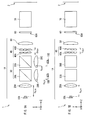
- FIGs. 1A and 1B are diagrams illustrating a schematic configuration of a projector according to a first embodiment of the disclosure.
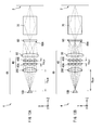
- FIGs. 2A and 2B are diagrams illustrating an example of light paths in the projector in FIGs. 1A and 1B .
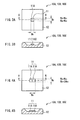
- FIGs. 3A and 3B are diagrams illustrating an example of a top surface configuration and a cross-sectional configuration of a light source in FIGs. 1A and 1B .
- FIGs. 4A and 4B are diagrams illustrating another example of the top surface configuration and the cross-sectional configuration of the light source in FIGs. 1A and 1B .
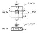
- FIGs. 5A and 5B are diagrams illustrating still another example of the top surface configuration and the cross-sectional configuration of the light source in FIGs. 1A and 1B .
- FIGs. 6A to 6C are diagrams illustrating an example of a light-emission spot of the light source in FIGs. 1A and 1B .
- FIGs. 7A and 7B are diagrams illustrating schematic configurations of fly-eye lenses in FIGs. 1A and 1B .
- FIG. 8 is a schematic diagram for describing a size of an illumination area in FIGs. 1A and 1B .
- FIG. 9 is a schematic diagram illustrating an example of light source images appearing in a fly-eye lens disposed backward in the projector in FIGs. 1A and 1B .
- FIGs. 10A and 10B are diagrams illustrating a schematic configuration of a projector according to a second embodiment of the disclosure.
- FIGs. 11A and 11B are diagrams illustrating an example of light paths in the projector in FIGs. 10A and 10B .
- FIGs. 12A and 12B are diagrams illustrating a schematic configuration of a projector according to a third embodiment of the disclosure.
- FIGs. 13A and 13B are diagrams illustrating an example of light paths in the projector in FIGs. 12A and 12B .
- FIGs. 14A and 14B are diagrams illustrating a schematic configuration of a projector according to a fourth embodiment of the disclosure.
- FIGs. 15A and 15B are diagrams illustrating an example of a cross-sectional configuration of a polarization splitter in FIGs. 14A and 14B .
- FIG. 16 is a diagram illustrating an example of a top surface configuration of a retardation plate array in FIGs. 14A and 14B .
- FIGs. 17A to 17C are diagrams illustrating an example of light paths in the projector in FIGs. 14A and 14B .
- FIG. 18 is a schematic diagram illustrating an example of light source images appearing in a fly-eye lens disposed backward in the projector in FIGs. 14A and 14B .
- FIG. 19 is a table illustrating designed values in examples according to the first to third embodiments.
- FIG. 20 is a table illustrating designed values in example according to the fourth embodiment.
- FIG. 21A is a diagram illustrating an example of a cross-sectional configuration of a modification of the light source according to each of the first to fourth embodiments
- FIG. 21B is a diagram illustrating a solid-state light-emitting device included in the light source of FIG. 21A , viewed from a light emission surface side.
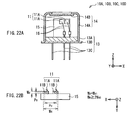
- FIG. 22A is a diagram illustrating another example of the cross-sectional configuration of the light source of FIG. 21A
- FIG. 22B is a diagram illustrating a solid-state light-emitting device included in the light source of FIG. 22A , viewed from a light emission surface side.
- FIG. 23A is a diagram illustrating still another example of the cross-sectional configuration of the light source of FIG. 21A
- FIG. 23B is a diagram illustrating a solid-state light-emitting device included in the light source of FIG. 23A , viewed from a light emission surface side.
- FIG. 24A is a diagram illustrating an example of a cross-sectional configuration of the light source of FIG. 21A , which is rotated by 90 degrees in XY plane
- FIG. 24B is a diagram illustrating a solid-state light-emitting device included in the light source of FIG. 24A , viewed from a light emission surface side.
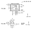
- FIG. 25A is a diagram illustrating an example of a cross-sectional configuration of the light source of FIG. 22A , which is rotated by 90 degrees in XY plane
- FIG. 25B is a diagram illustrating a solid-state light-emitting device included in the light source of FIG. 25A , viewed from a light emission surface side.
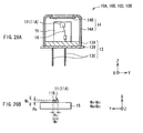
- FIG. 26A is a diagram illustrating an example of a cross-sectional configuration of the light source of FIG. 23A , which is rotated by 90 degrees in XY plane
- FIG. 26B is a diagram illustrating a solid-state light-emitting device included in the light source of FIG. 26A , viewed from a light emission surface side.
- FIG. 27 is a diagram illustrating a schematic configuration of a rear-projection display device using an illumination optical system according to any of the above-described embodiments.
- FIGs. 1A and 1B are diagrams illustrating a schematic configuration of a projector 1 according to a first embodiment of the disclosure.
- the projector 1 corresponds to a specific example of "a projection type display unit" in the disclosure.
- FIG. 1A illustrates a configuration example of the projector 1 viewed from above (from y-axis direction)
- FIG. 1B illustrates a configuration example of the projector 1 viewed from the side (from x-axis direction).
- FIGs. 2A and 2B are diagrams illustrating an example of light paths in the projector 1 of FIGs. 1A and 1B .
- FIG. 2A illustrates an example of light paths in the projector 1 viewed from above (from y-axis direction)
- FIG. 2B illustrates an example of light paths in the projector 1 viewed from the side (from x-axis direction).
- y-axis corresponds to a vertical direction
- x-axis corresponds to a horizontal direction
- y-axis may correspond to a horizontal direction
- x-axis may correspond to a vertical direction.
- the projector 1 includes, for example, an illumination optical system 1A, a spatial modulation device 60, and a projection optical system 70.
- the spatial modulation device 60 modulates light from the illumination optical system 1A based on an input picture signal to generate imaging light.
- the projection optical system 70 projects the imaging light generated by the spatial modulation device 60 onto a reflective screen 2.
- the illumination optical system 1A corresponds to a specific example of "an illumination unit”.
- the illumination optical system 1A supplies light flux illuminating an illumination area 60A (surface to be illuminated) of the spatial modulation device 60.
- any optical device may be provided in a region through which light of the illumination optical system 1A passes.
- a filter or the like for dimming light other than visible light of the light from the illumination optical system 1A may be provided.
- the illumination optical system 1A includes light sources 10A, 10B, and 10C, coupling lenses (traveling-direction angle conversion devices) 20A, 20B, and 20C, a light path unifying device 30, an integrator 40, and a condenser lens 50.
- the light path unifying device 30 unifies light beams from the light sources 10A, 10B and 10C, into a single light path, and is configured of, for example, two dichroic mirrors 30A and 30B.
- the integrator 40 equalizes illumination distribution of light in the illumination area 60A, and is configured of, for example, a pair of fly-eye lenses 40A and 40B.
- the coupling lens 20A, the light path unifying device 30, the integrator 40, and the condenser lens 50 are arranged in this order from the light source 10A side.
- An optical axis of the light source 10B is orthogonal to the optical axis of the light source 10A in the dichroic mirror 30A, and on the optical axis of the light source 10B, the coupling lens 20B and the dichroic mirror 30A are arranged in this order from the light source 10B side.
- An optical axis of the light source 10C is orthogonal to the optical axis of the light source 10A in the dichroic mirror 30B, and on the optical axis of the light source 10C, the coupling lens 20C and the dichroic mirror 30B are arranged in this order from the light source 10C side.
- FIGs. 1A and 1B although exemplified is a case where each components of the projector 1 (except for the light sources 10B and 10C, and the coupling lenses 20B and 20C) are arranged on a line parallel to z-axis, some components of the projector 1 may be arranged on a line not parallel to z-axis.
- the illumination optical system 1A may be arranged so that the optical axis of the illumination optical system 1A is along a direction orthogonal to z-axis by rotating the whole illumination optical system 1A by 90 degrees from a state of FIGs. 1A and 1B .
- an optical device for example, a mirror which directs light output from the illumination optical system 1A to the spatial modulation device 60 needs to be provided.
- the light source 10A, the coupling lens 20A, and the light path unifying device 30 may be arranged so that the optical axes of these components are along a direction orthogonal to z-axis by rotating these components by 90 degrees from the state of FIGs. 1A and 1B .
- an optical device for example, a mirror which directs light output from the light path unifying device 30 to the integrator 40 needs to be provided.
- the light sources 10A, 10B, and 10C each have a solid-state light-emitting device 11 and a package 12 supporting and covering the solid-state light-emitting device 11.
- the solid-state light-emitting device 11 emits light from a light emission region which is configured of one or more dot-like light-emission spots, or one or more non-dot-like light-emission spots.
- the solid-state light-emitting device 11 may be configured of a single chip 11A emitting light of a predetermined wavelength range, for example, as illustrated in FIGs.
- the solid-state light-emitting device 11 may be configured of a plurality of chips 11A emitting light of the same wavelength range or with different wavelength ranges, for example, as illustrated in FIGs. 4A and 4B and FIGs. 5A and 5B .
- the chips 11A are arranged in a lateral line, for example, as illustrated in FIGs. 4A and 4B , or are arranged in lateral and longitudinal directions, that is, in a lattice, for example, as illustrated in FIGs. 5A and 5B .
- the number of the chips 11A included in the solid-state light-emitting device 11 may be different for each of the light sources 10A, 10B, and 10C, or may be the same for all of the light sources 10A, 10B, and 10C.
- the size (W v *W H ) of the solid-state light-emitting device 11 is equal to the size (W v1 *W H1 ) of the single chip 11A, for example, as illustrated in FIG. 3A .
- the size of the solid-state light-emitting device 11 is equal to the size of the group, for example, as illustrated in FIG. 4A and FIG. 5A .
- the size (W v *W H ) of the solid-state light-emitting device 11 is W v )*2W H1 in the example of FIG. 4A .
- the size (W V *W H ) of the solid-state light-emitting device 11 is 2W V1 *2W H1 in the example of FIG. 5A .
- the chip 11A is configured with a light-emitting diode (LED), an organic EL light-emitting device (OLED), or a laser diode (LD). All chips 11A included in each of the light sources 10A, 10B, and 10C may be configured with LED, OLED, or LD. In addition, chips 11 A included in one or more of the light sources 10A, 10B, and 10C may be configured with LED, and chips 11A included in the other light source(s) may be configured with OLED. Moreover, chips 11A included in one or more of the light sources 10A, 10B, and 10C may be configured with LED, and chips 11A included in the other light source(s) may be configured with LD. Furthermore, chips 11 A included in one or more of the light sources 10A, 10B, and 10C may be configured with OLED, and chips 11A included in the other light source(s) may be configured with LD.
- the chips 11A included in each of the light sources 10A, 10B, and 10C each emit light of a wavelength range different for each of the light sources 10A, 10B, and 10C, for example.
- the chips 11A included in the light source 10A emit, for example, light with wavelength of approximately 400 nm to 500 nm (blue light).
- the chips 11A included in the light source 10B emit, for example, light with wavelength of approximately 500 nm to 600 nm (green light).
- the chips 11A included in the light source 10C emit, for example, light with wavelength of approximately 600 nm to 700 nm (red light).
- the chips 11A included in the light source 10A may emit light other than blue light (green light or red light).
- the chips 11A included in the light source 10B may emit light other than green light (blue light or red light).
- the chips 11A included in the light source 10C may emit light other than red light (green light or blue light).
- the chip 11A has a light-emission spot 11B with a size (P V1 *P H1 ) smaller than the size (W V1 *W H1 ) of the chip 11A.
- the light-emission spot 11B corresponds to a region (light emission region) from which the chip 11A emits light when a current is injected into the chip 11A to drive the chip 11A.
- the light-emission spot 11B has a non-dot-like shape (a planar shape), and in a case where the chip 11A is configured of LD, the light-emission spot 11B has a dot-like shape smaller than the light-emission spot 11B in the case of LED or OLED.
- the number of the light-emission spots 11 B is, for example, one as illustrated in FIG. 6A .
- the number of the light-emission spots 11B is equal to the number of the chips 11A, for example, as illustrated in FIGs. 6B and 6C .
- the size (P V *P H ) of the light emission region of the solid-state light-emitting device 11 is equal to the size (P V1 *P H1 ) of the light-emission spot 11B.
- the size (P V *P H ) of the light emission region as the solid-state light-emitting device 11 is equal to a size of an enclosure which encloses the light-emission spots 11B of all chips 11 A with a minimum inner area.
- the size (P V *P H ) of the light emission region is larger than P V1 *2P H1 but smaller than W V *W H in the example of FIG. 6B .
- the size (P V *P H ) of the light emission region is larger than 2P V1 *2P H1 but smaller than W V *W H in the example of FIG. 6C .
- the coupling lens 20A substantially parallelizes light emitted from the light source 10A, and converts a traveling-direction angle ( ⁇ H , ⁇ v ) of the light emitted from the light source 10A to be equal to or close to a traveling-direction angle of parallelized light.
- the coupling lens 20A is disposed on a position where light within the traveling-direction angle contained in the light emitted from the light source 10A enters the coupling lens 20A. As illustrated in FIGs.
- the coupling lens 20B substantially parallelizes light emitted from the light source 10B, and converts a traveling-direction angle ( ⁇ H , ⁇ v ) of the light emitted from the light source 10B to be equal to or close to a traveling-direction angle of parallelized light.
- the coupling lens 20B is disposed on a position allowing light within the traveling-direction angle of light emitted from the light source 10B to enter the coupling lens 20B. As illustrated in FIGs.
- the coupling lens 20C substantially parallelizes light emitted from the light source 10C, and converts a traveling-direction angle ( ⁇ H , ⁇ V ) of the light emitted from the light source 10C to be equal to or close to a traveling-direction angle of parallelized light.
- the coupling lens 20C is disposed on a position allowing light within the traveling-direction angle of light emitted from the light source 10C to enter the coupling lens 20C.
- the coupling lenses 20A, 20B, and 20C are arranged one to one for the light sources 10A, 10B, and 10C (for each package). Note that each of the coupling lenses 20A, 20B, and 20C may be configured of one or more lenses.
- the dichroic mirrors 30A and 30B each include a mirror with wavelength selectivity.
- the above-described mirror is configured by depositing a multilayer interference film.
- the dichroic mirror 30A allows light entering from the back side of the mirror (light entering from the light source 10A side) to pass therethrough to the front side of the mirror, and reflects light entering from the front side of the mirror (light entering from the light source 10B side) by the mirror.
- the dichroic mirror 30B allows light entering from the back side of the mirror (light of the light sources 10A and 10B entering from the dichroic mirror 30A side) to pass therethrough to the front side of the mirror, and reflects light entering from the front side of the mirror (light entering from the light source 10C side) by the mirror as illustrated in FIGs. 2A, and 2B , for example. Therefore, the light path unifying device 30 unifies individual light fluxes emitted from the light sources 10A, 10B, and 10C to generate a single light flux.
- Each of the cells 42 included in the fly-eye lens 40B is arranged to face each cell 41 of the fly-eye lens 40A.
- the fly-eye lens 40A is disposed on a focal position (or substantially on a focal position) of the fly-eye lens 40B, and the fly-eye lens 40B is disposed on a focal position (or substantially on a focal position) of the fly-eye lens 40A.
- light fluxes divided by the fly-eye lens 40A is each focused substantially on a lens surface of the image side of the fly-eye lens 40B, thereby forming secondary light source planes (light source images) on the focal point.
- the secondary light source planes are located on positions of a plane conjugate to an entrance pupil of the projection optical system 70.
- the secondary light source planes are, however, not necessarily located strictly on the positions of a plane conjugate to an entrance pupil of the projection optical system 70, and may be located within an acceptable region in design.
- the fly-eye lenses 40A and 40B may be integrally formed.
- Light fluxes emitted from the light sources 10A, 10B, and 10C generally show non-uniform intensity distribution on a plane perpendicular to the traveling direction of light fluxes. Therefore, if the light fluxes are directed as it is to the illumination area 60A (surface to be illuminated), illumination distribution in the illumination area 60A is non-uniform. However, as described above, when the light fluxes emitted from the light sources 10A, 10B, and 10C are divided into a plurality of light fluxes by the integrator 40 and then guided to the illumination area 60A in a superimposed manner, the illumination distribution in the illumination area 60A is allowed to be uniform.
- the condenser lens 50 collects light fluxes from multiple light sources formed by the integrator 40 to illuminate the illumination area 60A in a superimposed manner.
- the spatial modulation device 60 modulates light fluxes from the illumination optical system 1A two-dimensionally, based on a color image signal corresponding to wavelength component of each of the light sources 10A, 10B, and 10C, and thus generates imaging light.
- the spatial modulation device 60 is a transmissive device, and is configured of, for example, a transmissive liquid crystal panel.
- the spatial modulation device 60 may be configured of a reflective device such as a reflective liquid crystal panel and a digital micro mirror device. However, in such a case, light reflected by the spatial modulation device 60 needs to enter the projection optical system 70.
- the focal length of each of the coupling lenses 20A, 20B, and 20C, and the focal length of each of the fly-eye lenses 40A and 40B are set so that each light source image S formed on the fly-eye lens 40B by each cell 41 of the fly-eye lens 40A has a size not exceeding the size of one cell 42 of the fly-eye lens 40B.
- the relationship is schematically illustrated in FIG. 9 .
- FIG. 9 a case where each cell of the fly-eye lenses 40A and 40B has an aspect ratio other than 1 is illustrated. Incidentally, FIG. 9 will be described in detail later.
- P 1 is equal to a size of the light-emission spot 11B of the chip 11A.
- P 2 is equal to a size of the light-emission spot 11B of the chip 11A
- P 3 is equal to a size of the light-emission spot 11B of the chip 11A.
- P 1 is equal to a size of an enclosure which encloses the light-emission spots 11B of all chips 11A with a minimum inner area.
- P 2 is equal to a size of an enclosure which encloses the light-emission spots 11B of all chips 11A with a minimum inner area.
- P 3 is equal to a size of an enclosure which encloses the light-emission spots 11B of all chips 11A with a minimum inner area.
- f CL1 is a combined focal length of the lenses.
- f CL2 is a combined focal length of the lenses.
- f CL3 is a combined focal length of the lenses.
- W is equal to the size of the chip 11A.
- W is equal to the size of the single chip.
- each of the cells 41 and 42 of the fly-eye lenses 40A and 40B has an aspect ratio other than 1, it is preferable that the focal length of each of the coupling lenses 20A, 20B, and 20C and the focal length of each of the fly-eye lenses 40A and 40B satisfy the following six relational expressions.
- the ratio of horizontal focal length to vertical focal length of each of the coupling lenses 20A, 20B, and 20C (f CL1H /f CL1V , f CL2H /f CL2V , and f CL3H /f CL3V ) (anamorphic ratio) be equal to the inverse (h FEL2V /h FEL2H ) of the aspect ratio of the size of each cell 42 of the fly-eye lens 40B, and the illumination optical system 1A be an anamorphic optical system.
- FIG. 9 schematically illustrates the following expressions (7) to (12).
- a first direction or a direction corresponding thereto indicates the first direction in a case where the light sources 10A, 10B, and 10C and the coupling lenses 20A, 20B, and 20C are arranged on an optical axis of the integrator 40.
- a first direction or a direction corresponding thereto indicates the direction corresponding to the first direction because of layout of optical devices arranged on a light path from the light sources 10A, 10B, and 10C to the integrator 40, in a case where the light sources 10A, 10B, and 10C and the coupling lenses 20A, 20B, and 20C are arranged on a light path away from the optical axis of the integrator 40.
- a second direction or a direction corresponding thereto indicates the second direction in a case where the light sources 10A, 10B, and 10C and the coupling lenses 20A, 20B, and 20C are arranged on the optical axis of the integrator 40.
- a second direction or a direction corresponding thereto indicates the direction corresponding to the second direction because of the layout of the optical devices arranged on the light path from the light sources 10A, 10B, and 10C to the integrator 40, in the case where the light sources 10A, 10B, and 10C and the coupling lenses 20A, 20B, and 20C are arranged on a light path away from the optical axis of the integrator 40.
- P 1H is equal to a size in the first direction or a direction corresponding thereto, of the light-emission spot 11B of the chip 11A.
- P 2H is equal to a size in the first direction or a direction corresponding thereto, of the light-emission spot 11B of the chip 11A.
- P 3H is equal to a size in the first direction or a direction corresponding thereto, of the light-emission spot 11B of the chip 11A.
- P 1H is equal to a size in the first direction or a direction corresponding thereto, of an enclosure which encloses the light-emission spots 11B of all chips 11A with a minimum inner area.
- P 2H is equal to a size in the first direction or a direction corresponding thereto, of an enclosure which encloses the light-emission spots 11B of all chips 11A with a minimum inner area.
- P 3H is equal to a size in a first direction or a direction corresponding thereto, of an enclosure which encloses the light-emission spots 11B of all chips 11A with a minimum inner area.
- P 1V is equal to a size in the second direction or a direction corresponding thereto, of the light-emission spot 11B of the chip 11A.
- P 2V is equal to a size in the second direction or a direction corresponding thereto, of the light-emission spot 11B of the chip 11A.
- P 3V is equal to a size in the second direction or a direction corresponding thereto, of the light-emission spot 11B of the chip 11A.
- P 1V is equal to a size in the second direction or a direction corresponding thereto, of an enclosure which encloses the light-emission spots 11B of all chips 11A with a minimum inner area.
- P 2V is equal to a size in the second direction or a direction corresponding thereto, of an enclosure which encloses the light-emission spots 11B of all chips 11A with a minimum inner area.
- P 3V is equal to a size in the second direction or a direction corresponding thereto, of an enclosure which encloses the light-emission spots 11B of all chips 11A with a minimum inner area.
- the aspect ratio H/V of the illumination area 60A has a correlation with resolution of the spatial modulation device 60, and for example, when the resolution of the spatial modulation device 60 is VGA (640*480), the aspect ratio H/V is 640/480, and for example, when the resolution of the spatial modulation device 60 is WVGA (800*480), the aspect ratio H/V is 800/480.
- h FEL ⁇ 1 ⁇ H / h FEL ⁇ 1 ⁇ V H / V
- the focal length and the numerical aperture of each of the coupling lenses 20A, 20B, and 20C are set so that light entering the coupling lenses 20A, 20B, and 20C has a beam size not exceeding the size of the coupling lenses 20A, 20B, and 20C, respectively.
- the coupling lenses 20A, 20B, and 20C each have an aspect ratio other than 1, it is preferable that the focal length and the numerical aperture of each of the coupling lenses 20A, 20B, and 20C satisfy the following two relational expressions.
- the focal lengths F CL1 , f CL2 , and f CL3 of the coupling lenses 20A, 20B, and 20C and the focal length f FEL of each of the fly-eye lenses 40A and 40B are set so that each light source image S formed on the fly-eye lens 40B by each cell 41 of the fly-eye lens 40A has a size not exceeding the size of one cell 42 of the fly-eye lens 40B.
- the solid-state light-emitting device 11 I emits light from a light emission region configured of one or more dot-like light-emission spots, or one or more non-dot-like light-emission spots.
- the solid-state light-emitting device 11 is configured with, for example, one or more light-emitting diodes, one or more organic EL light-emitting devices, or one or more laser diodes. Therefore, even in a case where the fly-eye lens 40B is disposed on a focal position of the fly-eye lens 40A, each light source image S formed on the fly-eye lens 40B by each cell of the fly-eye lens 40A does not have a dot-like shape but has a certain size (see FIG. 9 ). However, in the embodiment, since one light source image S is not formed over a plurality of cells, light entering the fly-eye lens 40B reaches the illumination area efficiently. Accordingly, light use efficiency in the illumination optical system 1A may be improved.
- each cell of the fly-eye lenses 40A and 40B has an aspect ratio other than 1, when the focal lengths f CL1H, f CL2H , f CL3H , F CL1V , f CL2V , and f CL3V of the coupling lenses 20A, 20B, and 20C, and the focal lengths f FELH and f FELV of each of the fly-eye lenses 40A and 40B are set with the aspect ratio taken into consideration, light use efficiency in the illumination optical system 1A may be further improved.
- the coupling lenses 20A, 20B, and 20C each have an aspect ratio other than 1, when the focal lengths f CL1H , f CL2H , f CL3H, F CL1V, f CL2V , and f CL3V and the numbers of apertures NA 1H , NA 2H , NA 3H , NA 1V , NA 2V , and NA 3V of the coupling lenses 20A, 20B, and 20C are set with the aspect ratio taken into consideration, light use efficiency in the illumination optical system 1A may be further improved.
- the traveling-direction angles of the light sources 10A, 10B, and 10C are different from one another, when the focal lengths f CL1H , f CL2H , f CL3H , f CL1V , f CL2V , and f CL3V and the numbers of apertures NA 1H , NA 2H , NA 3 , NA 1V, NA 2V , and NA 3V of the coupling lenses 20A, 20B, and 20C are set with the traveling-direction angles taken into consideration, light use efficiency in the illumination optical system 1A may be further improved.
- FIGs. 10A and 10B illustrate a schematic configuration of a projector 3 according to a second embodiment of the disclosure.
- the projector 3 corresponds to a specific example of "a projection type display unit" in the disclosure.
- FIG. 10A illustrates a configuration example of the projector 3 viewed from above (from y-axis direction)
- FIG. 10B illustrates a configuration example of the projector 3 viewed from the side (x-axis direction).
- FIGs. 11A and 11B illustrate an example of light paths in the projector 3 of FIGs. 10A and 10B .
- FIG. 11A illustrates an example of the light paths of the projector 3 viewed from above (y-axis direction)
- FIG. 11B illustrates an example of the light paths of the projector 3 viewed from the side (x-axis direction).
- the projector 3 has a configuration different from the projector 1 having the illumination optical system 1A in that the projector 3 has an illumination optical system 3A. Accordingly, in the following description, different points from the projector 1 will be mainly described and the description of common points with the projector 1 will be appropriately omitted.
- the illumination optical system 3A includes a coupling lens 20D and a dichroic mirror 30C instead of the coupling lenses 20A, 20B, and 20C and the dichroic mirrors 30A and 30B in the illumination optical system 1A.
- the dichroic mirror 30C is disposed on a position where optical axes of the light sources 10A, 10B, and 10C intersect with one another.
- the coupling lens 20D is disposed on a light exit side of the dichroic mirror 30C and between the dichroic mirror 30C and the integrator 40.
- the dichroic mirror 30C includes two mirrors with wavelength selectivity. Note that the above-described mirrors are each configured by depositing multilayer interference film. The two mirrors are disposed to be orthogonal to each other so that the surfaces of the mirrors face the light exit side of the dichroic mirror 30C. As illustrated in FIGs. 11A and 11B , for example, the dichroic mirror 30C allows light (light entering from the light sources 10A and 10B side) entering from a back side of one of the mirrors (hereinafter, referred to as a mirror A for convenience) to pass therethrough to the front side of the mirror A, and reflects light entering from the front side of the mirror A (light entering from the light source 10C side) by the mirror A. In addition, as illustrated in FIGs.
- the dichroic mirror 30C allows light (light entering from the light sources 10A and 10C side) entering from a back side of the other mirror (hereinafter, referred to as a mirror B for convenience) to pass therethrough to the front side of the mirror B, and reflects light entering from the front side of the mirror B (light entering from the light source 10B side) by the mirror B. Therefore, the light path unifying device 30 unifies individual light fluxes emitted from the light sources 10A, 10B, and 10C to generate a single light flux.
- the coupling lens 20D substantially parallelizes light entering from the dichroic mirror 30C side, and converts a traveling-direction angle of the light entering from the dichroic mirror 30C to be equal to or close to a traveling-direction angle of parallelized light.
- the focal length f CL4 of the coupling lens 20D and the focal length f FEL of each of the fly-eye lenses 40A and 40B are set so that each light source image S formed on the fly-eye lens 40B by each cell of the fly-eye lens 40A has a size not exceeding the size of one cell of the fly-eye lens 40B. Therefore, as in the first embodiment, light use efficiency in the illumination optical system 3A may be improved.
- each cell of the fly-eye lenses 40A and 40B has an aspect ratio other than 1, when the focal lengths f CL4H and f CL4V of the coupling lens 20D and the focal lengths f FELH and f FELV of the fly-eye lenses 40A and 40B are set with the aspect ratio taken into consideration, light use efficiency in the illumination optical system 3A may be further improved.
- the coupling lens 20D has an aspect ratio other than 1, when the focal lengths f CL4H and f CL4V and the numerical aperture NA 4H and NA 4V of the coupling lens 20D are set with the aspect ratio taken into consideration, light use efficiency in the illumination optical system 3A may be further improved.
- focal lengths f CL1 , f CL2 , and f CL3 in the first embodiment are replaced by the focal length f CL4 of the coupling lens 20D in the second embodiment.
- focal lengths f CL1H , f CL2H , and f CL3H in the first embodiment are replaced by the focal length f CL4H in the first direction or a direction corresponding thereto, of the coupling lens 20D in the second embodiment.
- the focal lengths F CL1V , f CL2V , and f CL3V in the first embodiment are replaced by the focal length f CL4V in the second direction or a direction corresponding thereto, of the coupling lens 20D in the second embodiment.
- the beam sizes ⁇ CL1 , ⁇ CL2 , and ⁇ CL3 in the first embodiment are replaced by the beam size ⁇ PCL4 of light entering the coupling lens 20D in the second embodiment.
- the numbers of apertures NA 1 , NA 2 , and NA 3 in the first embodiment are replaced by the numerical aperture NA 4 of the coupling lens 20D in the second embodiment.
- the sizes h CL1 , h CL2 , and h CL3 in the first embodiment are replaced by a size h CL4 of the coupling lens 20D in the second embodiment.
- the beam sizes ⁇ CL1H , ⁇ CL2H , and ⁇ CL3H in the first embodiment are replaced by a beam size ⁇ CL4H in the first direction (for example, in the lateral direction) or a direction corresponding thereto, of light entering the coupling lens 20D in the second embodiment.
- the beam sizes ⁇ CL1V , ⁇ CL2V , and ⁇ CL3V in the first embodiment are replaced by a beam size ⁇ CL4V in the second direction (for example, in the longitudinal direction) or a direction corresponding thereto, of the light entering the coupling lens 20D in the second embodiment.
- the numerical apertures NA 1H , NA 2H , and NA 3H in the first embodiment are replaced by the numerical aperture NA 4H in the first direction or a direction corresponding thereto, of the coupling lens 20D in the second embodiment.
- the sizes h CL1H , h CL2H , and h CL3H in the first embodiment are replaced by a size h CL4H in the first direction or a direction corresponding thereto, of the coupling lens 20D in the second embodiment.
- the sizes h CL1V , h CL2V , and h CL3V in the first embodiment are replaced by a size h CL4V in the second direction or a direction corresponding thereto, of the coupling lens 20D in the second embodiment. Incidentally, these replacements are similarly performed in the subsequent embodiments.
- FIGs. 12A and 12B illustrate a schematic configuration of a projector 4 according to a third embodiment of the disclosure.
- the projector 4 corresponds to a specific example of "a projection type display unit" in the disclosure.
- FIG. 12A illustrates a configuration example of the projector 4 viewed from above (y-axis direction)
- FIG. 12B illustrates a configuration example of the projector 4 viewed from the side (x-axis direction).
- FIGs. 13A and 13B illustrate an example of light paths in the projector 4 of FIGs. 12A and 12B .
- FIG. 13A illustrates an example of the light paths of the projector 4 viewed from above (y-axis direction)
- FIG. 13B illustrates an example of the light paths of the projector 4 viewed from the side (x-axis direction).
- the projector 4 has a configuration different from the configuration of the projector 3 having the illumination optical system 3A in that the projector 4 includes an illumination optical system 4A. Therefore, in the following description, different points from the projector 3 will be mainly described and the description of common points to the projector 3 will be appropriately omitted.
- the illumination optical system 4A includes a light source 10D instead of the light sources 10A, 10B, and 10C, and the dichroic mirror 30C in the illumination optical system 3A.
- the light source 10D is arranged on the optical axis of the coupling lens 20D, and the illumination optical system 4A is configured to allow light emitted from the light source 10D to enter the coupling lens 20D directly.
- the light source 10D has, for example, the solid-state light-emitting device 11 and the package 12 which supports and covers the solid-state light-emitting device 11.
- the solid-state light-emitting device 11 included in the light source 10D emits light from a light emission region which is configured of one or more dot-like light-emission spots, or one or more non-dot-like light-emission spots.
- the solid-state light-emitting device 11 included in the light source 10D may be configured of, for example, a single chip 11A emitting light of a predetermined wavelength range, or a plurality of chips 11 A emitting light of the same wavelength range or different wavelength ranges.
- the solid-state light-emitting device 11 included in the light source 10D is configured of a plurality of chips 11A
- the chips 11A are arranged, for example, in lateral line, or in lateral and longitudinal directions, that is, in a lattice.
- the chip 11 A is configured of a light-emitting diode (LED), an organic EL light-emitting device (OLED), or a laser diode (LD).
- LED light-emitting diode
- OLED organic EL light-emitting device
- LD laser diode
- all chips 11A included in the light source 10D may be configured with one kind of LEDs, OLEDs, or LDs.
- some chips 11A may be configured with LEDs, and the other chips 11A may be configured with OLED.
- some chips 11A may be configured with LEDs, and the other chips 11A may be configured with LDs.
- some chips 11A may be configured with OLEDs
- the other chips 11A may be configured with LDs.
- some chips 11A may be configured with OLEDs
- the other chips 11 A may be configured with LDs.
- all chips 11 A included in the light source 10D may emit light of the same wavelength range or different wavelength ranges.
- all chips 11A may emit light with wavelength of approximately 400 nm to 500 nm (blue light), may emit light with wavelength of approximately 500 nm to 600 nm (green light), or may emit light with wavelength of approximately 600 nm to 700 nm (red light).
- the plurality of chips 11 A included in the light source 10D may be configured by combination of chips emitting light with wavelength of approximately 400 nm to 500 nm (blue light), chips emitting light with wavelength of approximately 500 nm to 600 nm (green light), and chips emitting light with wavelength of approximately 600 nm to 700 nm (red light).
- the focal length f CL4 of the coupling lens 20D and the focal length f FEL of each of the fly-eye lenses 40A and 40B are set so that each light source image S formed on the fly-eye lens 40B by each cell of the fly-eye lens 40A has a size not exceeding the size of one cell of the fly-eye lens 40B. Therefore, as in the second embodiment, light use efficiency in the illumination optical system 4A may be improved.
- each cell of the fly-eye lenses 40A and 40B has an aspect ratio other than 1, when the focal lengths f CL4H and f CL4V of the coupling lens 20D and the focal lengths f FELH and f FELV of the fly-eye lenses 40A and 40B are set with the aspect ratio taken into consideration, light use efficiency in the illumination optical system 4A may be further improved.
- the coupling lens 20D has an aspect ratio other than 1, when the focal lengths f CL4H and f CL4V and the numerical aperture NA 4H and NA 4V of the coupling lens 20D are set with the aspect ratio taken into consideration, light use efficiency in the illumination optical system 4A may be further improved.
- FIGs. 14A and 14B illustrate a schematic configuration of a projector 5 according to a fourth embodiment of the disclosure.
- the projector 5 corresponds to a specific example of "a projection type display unit" in the disclosure.
- FIG. 14A illustrates a configuration example of the projector 5 viewed from above (y-axis direction)
- FIG. 14B illustrates a configuration example of the projector 5 viewed from the side (x-axis direction).
- the projector 5 has a configuration different from that of the projector 4 having the illumination optical system 4A in that the projector 5 includes an illumination optical system 5A. Therefore, in the following description, different points from the projector 4 will be mainly described and the description of common points with the projector 4 will be appropriately omitted.
- the optical axes of the light source 10D and the coupling lens 20D are tilted to a direction intersecting the optical axis of the integrator 40.
- the optical axes of the light source 10D and the coupling lens 20D are preferably tilted to a lateral direction as illustrated in FIG. 14A .
- the optical axes of the light source 10D and the coupling lens 20D may be tilted to a longitudinal direction or may not be tilted.
- the illumination optical system 5A further includes a polarization splitter 80 and a retardation plate array 90.
- the polarization splitter 80 is disposed between the coupling lens 20D and the integrator 40
- the retardation plate array 90 is disposed between the integrator 40 and the condenser lens 50 (or the illumination area 60A).
- the fly-eye lens 40B is disposed a position which is closer to the fly-eye lens 40A relative to a position of the focal point of the fly-eye lens 40A
- the retardation plate array 90 is disposed on the focal point (or substantially on the focal point) of the fly-eye lens 40A.
- the polarization splitter 80 is an optical device with anisotropy to polarization of entering light, and splits (for example, diffracts) light entering from the coupling lens 20D side so that the traveling direction of S-polarization component is different from that of P-polarization component.
- the splitting direction of the polarization is preferably a lateral direction, however, may be a longitudinal direction.
- the polarization splitter 80 is preferably a polarization diffraction device having a concave-convex shape on one surface.
- the concave-convex shape is configured by arranging in parallel a plurality of strip-shaped convex sections with blade shape or step shape.
- the polarization splitter 80 may be a binary type polarization diffraction device, although not illustrated.
- the polarization splitter 80 allows light of S-polarization component contained in light entering from the coupling lens 20D side to pass therethrough so that an incident angle and an output angle of the light are equal to (or substantially equal to) each other. Moreover, the polarization splitter 80 allows light of P-polarization component contained in the light entering from the coupling lens 20D side to be diffracted and to pass therethrough so that the incident angle and the output angle of the light are different from each other. Note that the polarization splitter 80 may allow light of P-polarization component contained in the light entering from the coupling lens 20D side to pass therethrough so that the incident angle and the output angle of the light are equal to (or substantially equal to) each other, for example, in contradiction to the above-described example.
- the polarization splitter 80 may further allow light of S-polarization component contained in the light entering from the coupling lens 20D to be diffracted and to pass therethrough so that the incident angle and the output angle of the light are different from each other. It is preferable that the traveling direction of S-polarized light output from the polarization splitter 80 be opposite to and line symmetrical to the traveling direction of the P-polarized light output from the polarization splitter 80, in association with relationship with a normal (optical axis) of the polarization splitter 80.
- the retardation plate array 90 has first regions 90A and second regions 90B which have different phase differences.
- the first regions 90A are arranged in positions where either one of S- and P-polarization components, which are split by the polarization splitter 80, enters, and the first regions 90A allow light entering the first regions 90A to pass therethrough with maintaining the polarization direction.
- the second regions 90B are arranged in positions where polarization component different from the polarization component entering the first regions 90A of the S- and the P-polarization components, which are split by the polarization splitter 80, enters, and the second regions 90B convert light entering the second regions 90B into polarized light equivalent to polarized light of light entering the first regions 90A.
- the first regions 90A and the second regions 90B each have a strip shape extending in a direction orthogonal to a splitting (diffraction) direction by the polarization splitter 80, and are arranged alternately in a direction parallel to the splitting (diffraction) direction by the polarization splitter 80.
- each cell of the fly-eye lenses 40A and 40B has an aspect ratio other than 1
- both the first regions 90A and the second regions 90B preferably extend in a direction perpendicular to the longitudinal direction of the fly-eye lenses 40A and 40B.
- the total width ⁇ array of the first region 90A and the second region 90B which are adjacent to each other is, for example, equal to the width of one cell 42 of the fly-eye lens 40B.
- the total width A array thereof is, for example, equal to the width (h FEL2H ) in the lateral direction of the cell 42.
- the total width A array is, for example, equal to the width (h FEL2V ) in the longitudinal direction of the cell 42.
- the width H AWP1 of the first region 90A and the width h AWP2 of the second region 90B are equal to each other, for example.
- FIG. 17A schematically illustrates only light paths of S-polarization component or P-polarization component of the light having entered the polarization splitter 80
- FIG. 17B schematically illustrates only light paths of the polarization component different from the polarization component illustrated in FIG. 17A , contained in the light having entered the polarization splitter 80
- FIG. 17C schematically illustrates a state where the light paths are shared irrespective of the polarization component.
- light whose optical axis is tilted to a direction (for example, a lateral direction) parallel to an arrangement direction in the retardation plate array 90 enters the polarization splitter 80. Therefore, for example, as illustrated in FIGS. 17A and 17B , light of one of the polarization components contained in the light having entered the polarization splitter 80 is emitted in a direction parallel to an optical axis of incident light, and light of the other polarization component contained in the light having entered the polarization splitter 80 is emitted in a direction intersecting the optical axis of the incident light.
- a bisector of the optical axis of the light emitted in the direction parallel to the optical axis of the incident light and the optical axis of the light emitted in the direction intersecting the optical axis of the incident light is preferably parallel to (or substantially parallel to) a normal (z-axis) of the polarization splitter 80.
- Light emitted in the direction parallel to the optical axis of the incident light is divided into a plurality of fine light fluxes by the integrator 40 to enter the first regions 90A of the retardation plate array 90, for example, as illustrated in FIG. 17A .
- light emitted in the direction intersecting the optical axis of the incident light is divided into a plurality of fine light fluxes by the integrator 40 to enter, for example, the second regions 90B of the retardation plate array 90 as illustrated in FIG. 17B , for example.
- the light emitted in the direction parallel to the optical axis of the incident light may enter the second regions 90B of the retardation plate array 90 and the light emitted in the direction intersecting the optical axis of the incident light may enter the first regions 90A of the retardation plate array 90.
- one of the P-polarization light and S-polarization light is mainly emitted from the retardation plate array 90.
- the light emitted in the direction parallel to the optical axis of the incident light is divided into fine light fluxes by the fly-eye lens 40A, and then each of the divided light fluxes is focused substantially in the first regions 90A of the retardation plate array 90 to form secondary light source planes (light source images S A ) at this place (see FIG. 18 ).
- the light emitted in the direction intersecting the optical axis of the incident light is divided into fine light fluxes by the fly-eye lens 40A, and then each of the divided light fluxes is focused substantially in the second regions 90B of the retardation plate array 90 to form secondary light source planes (light source images S B ) at this place (see FIG. 18 ).
- the light source images configured of the light source images S A and S B correspond to the light source images S in the above-described embodiment.
- the focal length f CL4 of the coupling lens 20D and the focal length f FEL of each of the fly-eye lenses 40A and 40B are set so that each light source image S 1 and each light source image S 2 which is formed on the retardation plate array 90 by each cell 41 of the fly-eye lens 40A has a size not exceeding the size of one cell of the first region 90A and one cell of the second region 90B, respectively.
- P 4H is equal to a size in the first direction or a direction corresponding thereto, of the light-emission spot 11B of the chip 11A.
- P 4H is equal to a size in the first direction or a direction corresponding thereto, of an enclosure which encloses the light-emission spots 11B of the all chips 11A with a minimum inner area.
- f CL4H is the combined focal length in the first direction or a direction corresponding thereto, of the lenses.
- h H ⁇ 1 W 4 ⁇ H * f FEL / f CL ⁇ 4 ⁇ H ⁇ h AWP ⁇ 1
- h H ⁇ 2 W 4 ⁇ H * f FEL / f CL ⁇ 4 ⁇ H ⁇ h AWP ⁇ 2
- W 4H is a size in the first direction or a direction corresponding thereto, of the solid-state light-emitting device 11 included in the light source 10D.
- W 4H is equal to the size of the chip 11 A.
- W 4H is equal to the size of the single chip.
- the focal length f CL4 of the coupling lens 20D and the focal length f FEL of each of the fly-eye lenses 40A and 40B are set so that each light source image S 1 and each light source image S 2 formed on the retardation plate array 90 by each cell 41 of the fly-eye lens 40A has a size not exceeding the size of one cell of the first region 90A and one cell of the second region 90B, respectively. Accordingly, light use efficiency in the illumination optical system 5A may be improved.
- each cell of the fly-eye lenses 40A and 40B has an aspect ratio other than 1, when the focal lengths f CL4H and f CL4V of the coupling lens 20D and the focal lengths f FELH and f FELV of each of the fly-eye lenses 40A and 40B are set with the aspect ratio taken into consideration, light use efficiency in the illumination optical system 5A may be further improved.
- the coupling lens 20D has an aspect ratio other than 1, when the focal lengths f CL4H and f CL4V of the coupling lens 20D and the numbers of the apertures NA 4H and NA 4V are set with the aspect ratio taken into consideration, light use efficiency in the illumination optical system 5A may be further improved.
- the polarization splitter 80 is disposed in front of the integrator 40
- the retardation plate array 90 is disposed in the rear of the integrator 40, viewed from the light source 10D side, and light from the coupling lens 20D is allowed to enter the polarization splitter 80 in an oblique direction. Therefore, when a polarization plate is used on a light incident side or the like of the spatial modulation device 60, light emitted from the light source 10D is allowed to be converted into polarization light mainly containing polarization component parallel to a transmission axis of the polarization plate. As a result, light loss caused in the polarization plate, which is provided on the light incident side or the like of the spatial modulation device 60, may be decreased, and thus light use efficiency in the entire projector 5 may be substantially improved.
- FIG. 19 illustrates designed values of examples of the first to third embodiments
- FIG. 20 illustrates designed value of example of the fourth embodiment.
- Examples 1 to 3 in the figure correspond to the designed values common to the illumination optical systems 1A, 3A, and 4A
- example 4 in the figure corresponds to the designed values for the illumination optical system 5A.
- "Conditional Expressions" described at lowermost in FIG. 19 were obtained by substituting the designed values into the following expressions (27) to (29) and (31) to (33).
- f CL1H , f CL2H , f CL3H , and f CL4H were collectively described as f CLH for convenience, and F CL1V , f CL2V , f CL3V , and f CL4V were collectively described as f CLV for convenience.
- the numbers of the apertures NA 1H , NA 2H , NA 3H , and NA 4H were collectively described as NA H for convenience, and the numbers of the apertures NA 1V , NA 2V , NA 3V , and NA 4V were collectively described as NA V for convenience.
- any designed value may be used to set the focal lengths f CL1H , f CL2H , f CL3H , f CL4H , f CL1V , f CL2V , f CL3V , and fcL4v which satisfy the expressions (27) to (34), respectively.
- the chip 11 A may be an end-surface emission type element.
- the light sources 10A, 10B, 10C, and 10D each have a can-type structure in which a solid-state light-emitting device 11 configured of one or more end-surface emission type chips 11A is contained in an inner space enclosed by a stem 13 and a cap 14.
- the stem 13 configures, together with the cap 14, a package of the light source 10A, 10B, 10C, or 10D, and for example, includes a support substrate 13A supporting a sub mount 15, an outer frame substrate 13B disposed on the rear surface of the support substrate 13A, and a plurality of connection terminals 13C.
- the sub mount 15 is made of a material having conductivity and heat radiation property.
- the support substrate 13A and the outer frame substrate 13B are each configured by forming one or more insulation through-holes and one or more conductive through-holes on a substance having conductivity and heat radiation property.
- Each of the support substrate 13A and the outer frame substrate 13B has, for example, a disc-like shape, and are stacked so that central axes (not illustrated) of both substrates are coincident with each other.
- the outer frame substrate 13B has a diameter larger than that of the support substrate 13A.
- the outer edge of the outer frame substrate 13B is a circular flange projecting toward a radiation direction from the central axis thereof in a plane whose normal is the central axis of the outer frame substrate 13B.
- the flange has a function of defining a reference position for fitting the cap 14 in the support substrate 13A in manufacturing process.
- the plurality of connection terminals 13C penetrates at least the support substrate 13A.
- Terminals except for one or more terminals of the connection terminals 13C are electrically connected to electrodes (not illustrated) of the individual chips 11 A, respectively.
- the terminals ⁇ project long toward the outer frame substrate 13B side and project short toward the support substrate 13A side.
- terminals other than the above-described terminals ⁇ of the connection terminals 13C are electrically connected to the other electrodes (not illustrated) of all chips 11A.
- the terminals ⁇ project long toward the outer frame substrate 13B side and the end edges on the support substrate 13A side of the terminals ⁇ are embedded in the support substrate 13A.
- a portion projecting long toward the outer frame substrate 13B side corresponds to, for example, a portion embedded in the substrate or the like.
- a portion projecting short toward the support substrate 13A side corresponds to a portion electrically connected one-to-one to the chip 11A through a wire 16.
- a portion embedded in the support substrate 13A corresponds to, for example, a portion electrically connected to all chips 11A through the support substrate 13A and the sub mount 15.
- the terminals ⁇ are supported by the insulation through-holes provided in the support substrate 13A and the outer frame substrate 13B, and the through-hole insulates and separates the terminals ⁇ from the support substrate 13A and the outer frame substrate 13B. Moreover, the terminals ⁇ are insulated and separated from each other by the above-described insulation member. On the other hand, the terminals ⁇ are supported by the conductive through-holes provided in the support substrate 13A and the outer frame substrate 13B, and are electrically connected to the through-holes.
- the cap 14 seals the solid-state light-emitting device 11.
- the cap 14 has, for example, a cylindrical portion 14A provided with apertures on a top and a bottom thereof.
- the bottom of the cylindrical portion 14A is, for example, in contact with a side surface of the support substrate 13A, and the solid-state light-emitting device 11 is positioned in an inner space of the cylindrical portion 14A.
- the cap 14 has a light transmission window 14B arranged so as to cover the aperture on the top of the cylindrical portion 14A.
- the light transmission window 14B is disposed on a position facing to the light emission surface of the solid-state light-emitting device 11, and has a function of transmitting light output from the solid-state light-emitting device 11.
- the solid-state light-emitting device 11 emits light from the light emission region configured of one or more dot-like light-emission spots, or one or more non-dot-like light-emission spots.
- the solid-state light-emitting device 11 may be configured of, for example, a single chip 11A emitting light of a predetermined wavelength range, a plurality of chips 11A emitting light of the same wavelength range, or a plurality of chips 11 A emitting light of different wavelength ranges.
- the chips 11A are arranged in a lateral line as illustrated in FIGs. 21 A and 21B and FIGs.
- the number of the chips 11A included in the solid-state light-emitting device 11 may be different or the same in the light sources 10A, 10B, 10C, and 10D.
- the size (W V *W H ) of the solid-state light-emitting device 11 is equal to the size (W V1 *W H1 ) of the single chip 11A as illustrated in FIGs. 23B and 26B , for example.
- the size of the solid-state light-emitting device 11 is equal to the size of the group as illustrated in FIGs. 21B , 22B , 24B , and 25B , for example.
- the size (W V *W H ) of the solid-state light-emitting device 11 is larger than W V1 *3W H1 in the example of FIG. 21B , and is larger than W V1 *2W H1 in the example of FIG. 22B .
- the size (W V *W H ) of the solid-state light-emitting device 11 is larger than 3W V1 *W H1 in the example of FIG. 24B , and is larger than 2W V1 *W H1 in the example of the FIG. 25B .
- the chip 11A is configured with, for example, a laser diode (LD). All chips 11A included in the light sources 10A, 10B, 10C, and 10D may be configured with LDs. Moreover, chips 11A included in one or more of the light sources 10A, 10B, 10C, and 10D may be configured with LDs, and chips 11A included in other light sources may be configured with LEDs or OLEDs.
- LD laser diode
- each of the chips 11A includes the light-emission spot 11B having a size (P V1 *P H1 ) smaller than the size (W V *W H ) of the chip 11A.
- the light-emission spot 11B corresponds to a region (light emission region) in which light is emitted from the chip 11A when a current is injected into the chip 11A to drive the chip 11A.
- the light-emission spot 11B is a dot-like shape smaller than the light-emission spot of the LED or OLED.
- the number of the light-emission spot 11B is one as illustrated in FIGs. 23B and 26B , for example.
- the number of the light-emission spots 11B is equal to the number of the chips 11A as illustrated in FIGs. 21B , 22B , 24B , and 25B , for example.
- the size (P V *P H ) of the light emission region as the solid-state light-emitting device 11 is equal to the size (P V1 *P H1 ) of the light-emission spot 11B.
- the size (P V *P H ) of the light emission region as the solid-state light-emitting device 11 is equal to the size of an enclosure which encloses the light-emission spots 11B of all chips 11A with a minimum inner area.
- the size (P V *P H ) of the light emission region is larger than P V1 *3P H1 but smaller than W V *W H in the example of the FIG. 21B .
- the size (P V *P H ) of the light emission region is larger than P V1 *2P H1 but smaller than W V *W H .
- the size (P V *P H ) of the light emission region is larger than 3P V1 *P H1 but smaller than W V *W H in the example of FIG. 24B .
- the size (P V *P H ) of the light emission region is larger than 2P V1 *P H1 but smaller than W V *W H .
- the illumination optical systems 1A, 3A, 4A, and 5A each are configured to include infinite optical system allowing parallelized light to enter the fly-eye lens 40A
- the illumination optical systems 1A, 3A, 4A, and 5A each may be configured to include finite optical system allowing convergent light (or divergent light) to enter the fly-eye lens 40A.
- a traveling-direction angle conversion device having a function of focusing or dispersing light emitted from the light sources 10A to 10D may be disposed.
- an optical magnification of the optical system configured with the above-described traveling-direction angle conversion device and the fly-eye lenses 40A and 40B be set so that each light source image S formed on the fly-eye lens 40B by each cell 41 of the fly-eye lens 40A has a size not exceeding the size of one cell 42 of the fly-eye lens 40B.
- the optical magnification of the optical system configured with the above-described traveling-direction angle conversion device and the fly-eye lenses 40A and 40B satisfy the following relational expression.
- h P ⁇ m ⁇ h FEL ⁇ 2
- m is an optical magnification of the optical system configured with the above-described traveling-direction angle conversion device and the fly-eye lenses 40A and 40B.
- the illumination optical systems 1A, 3A, 4A, and 5A each are preferably an anamorphic optical system.
- the present technology is surely applicable to other display devices.
- the present technology is applicable to a rear-projection display device 6.
- the rear-projection display device 6 includes the projector 1, 3, 4, or 5 including the illumination optical system 1A, 3A, 4A, or 5A, respectively, and a transmissive screen 7 displaying imaging light projected from the projector 1, 3, 4, or 5 (projection optical system 70) as illustrated in FIG. 27 .
- the illumination optical system 1A, 3A, 4A, or 5A is used as the illumination optical system of the rear-projection display system 6 so that light use efficiency may be improved.
Landscapes
- Physics & Mathematics (AREA)
- General Physics & Mathematics (AREA)
- Optics & Photonics (AREA)
- Engineering & Computer Science (AREA)
- Multimedia (AREA)
- Signal Processing (AREA)
- Microelectronics & Electronic Packaging (AREA)
- General Engineering & Computer Science (AREA)
- Projection Apparatus (AREA)
- Non-Portable Lighting Devices Or Systems Thereof (AREA)
- Led Device Packages (AREA)
- Semiconductor Lasers (AREA)
Abstract
Description
- This disclosure relates to an illumination unit using a solid-state light-emitting device such as a light-emitting diode (LED), and a projection type display unit and a direct view type display unit including the same.
- In recent years, projectors projecting pictures onto a screen have been widely used in homes besides offices. The projector modulates light from a light source with use of a light valve to generate imaging light, and projects the imaging light onto a screen, thereby performing display. Nowadays, palm-sized ultra-compact projectors, mobile phones with a built-in ultra-compact projector, and the like are being introduced.
- Incidentally, as a light source used in a projector, a discharge lamp with high luminance is standard. The discharge lamp, however, is relatively large in size and consumes larger power. Therefore, as a light source alternative to the discharge lamp, solid-state light-emitting devices such as a light-emitting diode (LED), a laser diode (LD), and an organic EL (OLED) has been attracted attention (for example, Japanese Unexamined Patent Application Publication No.
2008-134324 - In a case where the above-described solid-state light-emitting device is used as a light source of a projector, it is considered that other main components included in the projector are also downsized to further downsize the projector itself. However, when the other main components included in the projector are downsized, light use efficiency is likely to be lowered. Therefore, for example, even if light amount of a light source is increased by increasing the number of the above-described solid-state light-emitting devices, there is a possibility to raise an issue that desired luminance is not obtained due to the lowering of light use efficiency.
- It is desirable to provide a small illumination unit with improved light use efficiency. In addition, it is desirable to provide a projection type display unit and a direct view type display unit using such a small illumination unit.
Various respective aspects and features of the invention are defined in the appended claims. - An illumination unit according to an embodiment of the disclosure includes one or more light sources each including a solid-state light-emitting device having a light emission region configured of one or more light-emission spots, one or more traveling-direction angle conversion device each converting a traveling-direction-angle of light entering from the solid-state light-emitting device, and an integrator including a first fly-eye lens having cells which receive light from the traveling-direction angle conversion device and a second fly-eye lens having cells which receive light from the first fly-eye lens. The integrator uniformalizes illumination distribution in a predetermined illumination area which is to be illuminated by light from the traveling-direction angle conversion device. An optical system configured with the traveling-direction angle conversion device and the first and second fly-eye lenses has an optical magnification which allows each of light source images to have a size not exceeding a size of the cell in the second fly-eye lens, the light source images being formed on the second fly-eye lens by the respective cells in the first fly-eye lens.
- A projection type display unit according to an embodiment of the disclosure includes: an illumination optical system; a spatial modulation device modulating light from the illumination optical system based on an input picture signal to generate imaging light; and a projection optical system projecting the imaging light generated by the spatial modulation device. The illumination optical system included in the projection type display unit has the same components as those in the above-described illumination unit.
- A direct view type display unit according to an embodiment of the disclosure includes: an illumination optical system; a spatial modulation device modulating light from the illumination optical system based on an input picture signal to generate imaging light; a projection optical system projecting the imaging light generated by the spatial modulation device; and a transmissive screen displaying the imaging light projected from the projection optical system. The illumination optical system included in the direct view type display unit has the same components as those in the above-described illumination unit.
- In the illumination unit, the projection type display unit, and the direct view type display unit according to the embodiment of the disclosure, an optical magnification of an optical system configured with the traveling-direction angle conversion device and the first and second fly-eye lenses is set so that each light source image formed on the second fly-eye lens by each cell of the first fly-eye lens has a size not exceeding a size of one cell of the second fly-eye lens. Therefore, light entering the second fly-eye lens efficiently reaches the illumination area.
- In the illumination unit, the projection type display unit, and the direct view type display unit according to the embodiment of the disclosure, in a case where the solid-state light-emitting device is configured of a single chip which emits light in a predetermined wavelength range or is configured of a plurality of chips which emit light in the same wavelength range or different wavelength ranges, the optical magnification of the optical system configured with the traveling-direction angle conversion device and the first and second fly-eye lenses preferably satisfies the following expression:

where h is a size of the light source image, - P is a size of the light emission region (the size is equal to a size of a light-emission spot of the chip when the solid-state light-emitting device is configured of one chip, and the size is equal to a size of an enclosure which encloses light-emission spots of all the chips with a minimum inner area when the solid-state light-emitting device is configured of a plurality of chips),
- m is an optical magnification of an optical system configured with the traveling-direction angle conversion device and the first and second fly-eye lenses, and
- hFEL2 is a size of the cell in the second fly-eye lens.
- In the illumination unit, the projection type display unit, and the direct view type display unit according to the embodiment of the disclosure, in a case where the traveling-direction angle conversion device converts a traveling-direction angle of light entering from the solid-state light-emitting device to be equal to or close to a traveling-direction angle of parallelized light, a focal length of the traveling-direction angle conversion device and a focal length of each of the first and the second fly-eye lenses preferably satisfy the following expression. At this time, in a case where each cell of the first and second fly-eye lenses has an aspect ratio other than 1, the focal length of the traveling-direction angle conversion device and the focal length of each of the first and second fly-eye lenses are preferably set with the aspect ratio taken into consideration.

where - fFEL is a focal length of each of the first and second fly-eye lenses, and
- fCL is a focal length of the traveling-direction angle conversion device.
- In the illumination unit, the projection type display unit, and the direct view type display unit according to the embodiment of the disclosure, the traveling-direction angle conversion device has a focal length and a numerical aperture which allow light which enters thereto to have a beam size not exceeding a size of the traveling-direction angle conversion device. In this case, the focal length and the numerical aperture of the traveling-direction angle conversion device preferably satisfy the following expression. At this time, in a case where the traveling-direction angle conversion device has an aspect ratio other than 1, the focal length and the numerical aperture of the traveling-direction angle conversion device are preferably set with the aspect ratio taken into consideration.

where - ϕCL is a beam size of light entering the traveling-direction angle conversion device,
- NA is the numerical aperture of the traveling-direction angle conversion device, and
- hCL is a size of the traveling-direction angle conversion device.
- In the illumination unit, the projection type display unit, and the direct view type display unit according to the embodiment of the disclosure, in a case where a plurality of light sources and a plurality of traveling-direction angle conversion devices are provided, each of the light sources may be formed in a manner of a package including the solid-state light-emitting device therein, and each of the traveling-direction angle conversion devices may be arranged for each of the packages. In this case, the illumination unit preferably further includes a light path unifying device unifying light beams, which have passed through the respective traveling-direction angle conversion devices, into a single light path. In addition, in the illumination unit, the projection type display unit, and the direct view type display unit according to the embodiment of the disclosure, in a case where a plurality of light sources and one traveling-direction angle conversion device are provided, each of the light sources may be formed in a manner of a package including the solid-state light-emitting device therein. In this case, the illumination unit preferably further includes a light path unifying device unifying light emitted from each solid-state light-emitting device, into a single light path. Moreover, in the illumination unit, the projection type display unit, and the direct view type display unit according to the embodiment of the disclosure, in a case where one light source and one traveling-direction angle conversion device are provided, the light source may be formed in a manner of a package including the solid-state light-emitting device therein. Furthermore, in the illumination unit, the projection type display unit, and the direct view type display unit according to the embodiment of the disclosure, the chip may be configured with a light emitting diode, an organic EL light-emitting device, or a laser diode. Moreover, in the illumination unit, the projection type display unit, and the direct view type display unit according to the embodiment of the disclosure, a ratio of a vertical magnification factor to a horizontal magnification factor of the traveling-direction angle conversion device may be equal to an inverse of the aspect ratio of each cell in the second fly-eye lenses.
- According to the illumination unit, the projection type display unit, and the direct view type display unit of the embodiment of the disclosure, since one light source image is not formed over a plurality of cells, light use efficiency in the illumination unit may be improved.
- In addition, in the illumination unit, the projection type display unit, and the direct view type display unit according to the embodiment of the disclosure, in the case where each cell of the first and second fly-eye lenses has an aspect ratio other than 1, when the focal length of the traveling-direction angle conversion device and the focal length of each of the first and second fly-eye lenses are set with the aspect ratio taken into consideration, light use efficiency in the illumination unit may be further improved. Moreover, in the illumination unit, the projection type display unit, and the direct view type display unit according to the embodiment of the disclosure, in a case where the traveling-direction angle conversion device has an aspect ratio other than 1, when the focal length and the numerical aperture of the traveling-direction angle conversion device are set with the aspect ratio taken into consideration, light use efficiency in the illumination unit may be further improved.
- It is to be understood that both the foregoing general description and the following detailed description are exemplary, and are intended to provide further explanation of the technology as claimed.
- The accompanying drawings are included to provide a further understanding of the disclosure, and are incorporated in and constitute a part of this specification. The drawings illustrate embodiments and, together with the specification, serve to explain the principles of the technology.
-
FIGs. 1A and 1B are diagrams illustrating a schematic configuration of a projector according to a first embodiment of the disclosure. -
FIGs. 2A and 2B are diagrams illustrating an example of light paths in the projector inFIGs. 1A and 1B . -
FIGs. 3A and 3B are diagrams illustrating an example of a top surface configuration and a cross-sectional configuration of a light source inFIGs. 1A and 1B . -
FIGs. 4A and 4B are diagrams illustrating another example of the top surface configuration and the cross-sectional configuration of the light source inFIGs. 1A and 1B . -
FIGs. 5A and 5B are diagrams illustrating still another example of the top surface configuration and the cross-sectional configuration of the light source inFIGs. 1A and 1B . -
FIGs. 6A to 6C are diagrams illustrating an example of a light-emission spot of the light source inFIGs. 1A and 1B . -
FIGs. 7A and 7B are diagrams illustrating schematic configurations of fly-eye lenses inFIGs. 1A and 1B . -
FIG. 8 is a schematic diagram for describing a size of an illumination area inFIGs. 1A and 1B . -
FIG. 9 is a schematic diagram illustrating an example of light source images appearing in a fly-eye lens disposed backward in the projector inFIGs. 1A and 1B . -
FIGs. 10A and 10B are diagrams illustrating a schematic configuration of a projector according to a second embodiment of the disclosure. -
FIGs. 11A and 11B are diagrams illustrating an example of light paths in the projector inFIGs. 10A and 10B . -
FIGs. 12A and 12B are diagrams illustrating a schematic configuration of a projector according to a third embodiment of the disclosure. -
FIGs. 13A and 13B are diagrams illustrating an example of light paths in the projector inFIGs. 12A and 12B . -
FIGs. 14A and 14B are diagrams illustrating a schematic configuration of a projector according to a fourth embodiment of the disclosure. -
FIGs. 15A and 15B are diagrams illustrating an example of a cross-sectional configuration of a polarization splitter inFIGs. 14A and 14B . -
FIG. 16 is a diagram illustrating an example of a top surface configuration of a retardation plate array inFIGs. 14A and 14B . -
FIGs. 17A to 17C are diagrams illustrating an example of light paths in the projector inFIGs. 14A and 14B . -
FIG. 18 is a schematic diagram illustrating an example of light source images appearing in a fly-eye lens disposed backward in the projector inFIGs. 14A and 14B . -
FIG. 19 is a table illustrating designed values in examples according to the first to third embodiments. -
FIG. 20 is a table illustrating designed values in example according to the fourth embodiment. -
FIG. 21A is a diagram illustrating an example of a cross-sectional configuration of a modification of the light source according to each of the first to fourth embodiments, andFIG. 21B is a diagram illustrating a solid-state light-emitting device included in the light source ofFIG. 21A , viewed from a light emission surface side. -
FIG. 22A is a diagram illustrating another example of the cross-sectional configuration of the light source ofFIG. 21A , andFIG. 22B is a diagram illustrating a solid-state light-emitting device included in the light source ofFIG. 22A , viewed from a light emission surface side. -
FIG. 23A is a diagram illustrating still another example of the cross-sectional configuration of the light source ofFIG. 21A , andFIG. 23B is a diagram illustrating a solid-state light-emitting device included in the light source ofFIG. 23A , viewed from a light emission surface side. -
FIG. 24A is a diagram illustrating an example of a cross-sectional configuration of the light source ofFIG. 21A , which is rotated by 90 degrees in XY plane, andFIG. 24B is a diagram illustrating a solid-state light-emitting device included in the light source ofFIG. 24A , viewed from a light emission surface side. -
FIG. 25A is a diagram illustrating an example of a cross-sectional configuration of the light source ofFIG. 22A , which is rotated by 90 degrees in XY plane, andFIG. 25B is a diagram illustrating a solid-state light-emitting device included in the light source ofFIG. 25A , viewed from a light emission surface side. -
FIG. 26A is a diagram illustrating an example of a cross-sectional configuration of the light source ofFIG. 23A , which is rotated by 90 degrees in XY plane, andFIG. 26B is a diagram illustrating a solid-state light-emitting device included in the light source ofFIG. 26A , viewed from a light emission surface side. -
FIG. 27 is a diagram illustrating a schematic configuration of a rear-projection display device using an illumination optical system according to any of the above-described embodiments. - Hereinafter, preferred embodiments of the technology will be described in detail with reference to drawings. Note that the description will be given in the following order.
- 1. First embodiment (
FIGs. 1A and 1B toFIG. 9 )
Example of unifying light beams from each light source into a single light path after parallelization of light with use of coupling lenses - 2. Second embodiment (
FIGs. 10A and 10B andFIGs. 11A and 11B )
Example of unifying light beams from each light source into a single light path before parallelization of light with use of coupling lenses - 3. Third embodiment (
FIGs. 12A and 12B andFIGs. 13A and 13B )
Example of emitting light of different wavelength ranges from a single package to eliminate unification of light paths - 4. Fourth embodiment (
FIGs. 14A and 14B toFIG. 18 )
Example in which a polarization splitter and a retardation plate array are provided - 5. Examples (
FIG. 19 and FIG. 20 ) - 6. Modifications (
FIGs. 21A and 21B toFIG. 27 ) -
FIGs. 1A and 1B are diagrams illustrating a schematic configuration of aprojector 1 according to a first embodiment of the disclosure. Note that theprojector 1 corresponds to a specific example of "a projection type display unit" in the disclosure.FIG. 1A illustrates a configuration example of theprojector 1 viewed from above (from y-axis direction), andFIG. 1B illustrates a configuration example of theprojector 1 viewed from the side (from x-axis direction).FIGs. 2A and 2B are diagrams illustrating an example of light paths in theprojector 1 ofFIGs. 1A and 1B .FIG. 2A illustrates an example of light paths in theprojector 1 viewed from above (from y-axis direction) andFIG. 2B illustrates an example of light paths in theprojector 1 viewed from the side (from x-axis direction). - Typically, y-axis corresponds to a vertical direction, and x-axis corresponds to a horizontal direction, however, y-axis may correspond to a horizontal direction and x-axis may correspond to a vertical direction. Note that in the following description, for convenience, the description will be given on the assumption that the y-axis corresponds to a vertical direction and x-axis corresponds to a horizontal direction. In addition, in the following description, it is assumed that "lateral direction" indicates x-axis direction and "longitudinal direction" indicates y-axis direction.
- The
projector 1 includes, for example, an illuminationoptical system 1A, aspatial modulation device 60, and a projectionoptical system 70. Thespatial modulation device 60 modulates light from the illuminationoptical system 1A based on an input picture signal to generate imaging light. The projectionoptical system 70 projects the imaging light generated by thespatial modulation device 60 onto areflective screen 2. Note that the illuminationoptical system 1A corresponds to a specific example of "an illumination unit". - The illumination
optical system 1A supplies light flux illuminating anillumination area 60A (surface to be illuminated) of thespatial modulation device 60. Note that, if necessary, any optical device may be provided in a region through which light of the illuminationoptical system 1A passes. For example, in a region though which light of the illuminationoptical system 1A passes, a filter or the like for dimming light other than visible light of the light from the illuminationoptical system 1A may be provided. - As illustrated in
FIGs. 1A and 1B , for example, the illuminationoptical system 1A includeslight sources unifying device 30, anintegrator 40, and acondenser lens 50. The light pathunifying device 30 unifies light beams from thelight sources dichroic mirrors integrator 40 equalizes illumination distribution of light in theillumination area 60A, and is configured of, for example, a pair of fly-eye lenses light source 10A, thecoupling lens 20A, the light pathunifying device 30, theintegrator 40, and thecondenser lens 50 are arranged in this order from thelight source 10A side. An optical axis of thelight source 10B is orthogonal to the optical axis of thelight source 10A in thedichroic mirror 30A, and on the optical axis of thelight source 10B, thecoupling lens 20B and thedichroic mirror 30A are arranged in this order from thelight source 10B side. An optical axis of thelight source 10C is orthogonal to the optical axis of thelight source 10A in thedichroic mirror 30B, and on the optical axis of thelight source 10C, thecoupling lens 20C and thedichroic mirror 30B are arranged in this order from thelight source 10C side. - Note that in
FIGs. 1A and 1B , although exemplified is a case where each components of the projector 1 (except for thelight sources coupling lenses projector 1 may be arranged on a line not parallel to z-axis. For example, although not illustrated, the illuminationoptical system 1A may be arranged so that the optical axis of the illuminationoptical system 1A is along a direction orthogonal to z-axis by rotating the whole illuminationoptical system 1A by 90 degrees from a state ofFIGs. 1A and 1B . However, in this case, an optical device (for example, a mirror) which directs light output from the illuminationoptical system 1A to thespatial modulation device 60 needs to be provided. Moreover, for example, thelight source 10A, thecoupling lens 20A, and the light pathunifying device 30 may be arranged so that the optical axes of these components are along a direction orthogonal to z-axis by rotating these components by 90 degrees from the state ofFIGs. 1A and 1B . However, also in this case, an optical device (for example, a mirror) which directs light output from the light pathunifying device 30 to theintegrator 40 needs to be provided. - As illustrated in
FIGs. 3A and 3B toFIGs. 5A and 5B , for example, thelight sources device 11 and apackage 12 supporting and covering the solid-state light-emittingdevice 11. The solid-state light-emittingdevice 11 emits light from a light emission region which is configured of one or more dot-like light-emission spots, or one or more non-dot-like light-emission spots. The solid-state light-emittingdevice 11 may be configured of asingle chip 11A emitting light of a predetermined wavelength range, for example, as illustrated inFIGs. 3A and 3B , or may be configured of a plurality ofchips 11A emitting light of the same wavelength range or with different wavelength ranges, for example, as illustrated inFIGs. 4A and 4B andFIGs. 5A and 5B . In a case where the solid-state light-emittingdevice 11 is configured of a plurality ofchips 11A, thechips 11A are arranged in a lateral line, for example, as illustrated inFIGs. 4A and 4B , or are arranged in lateral and longitudinal directions, that is, in a lattice, for example, as illustrated inFIGs. 5A and 5B . The number of thechips 11A included in the solid-state light-emittingdevice 11 may be different for each of thelight sources light sources - In a case where the solid-state light-emitting
device 11 is configured of asingle chip 11A, the size (Wv*WH) of the solid-state light-emittingdevice 11 is equal to the size (Wv1*WH1) of thesingle chip 11A, for example, as illustrated inFIG. 3A . On the other hand, in a case where the solid-state light-emittingdevice 11 is configured of a plurality ofchips 11A, when allchips 11A are regarded as one group, the size of the solid-state light-emittingdevice 11 is equal to the size of the group, for example, as illustrated inFIG. 4A andFIG. 5A . In a case where the plurality ofchips 11A are arranged in a lateral line, the size (Wv*WH) of the solid-state light-emittingdevice 11 is Wv)*2WH1 in the example ofFIG. 4A . Moreover, in a case where the plurality ofchips 11A are arranged in the lateral and longitudinal directions, that is, in a lattice, the size (WV*WH) of the solid-state light-emittingdevice 11 is 2WV1*2WH1 in the example ofFIG. 5A . - The
chip 11A is configured with a light-emitting diode (LED), an organic EL light-emitting device (OLED), or a laser diode (LD). Allchips 11A included in each of thelight sources light sources chips 11A included in the other light source(s) may be configured with OLED. Moreover,chips 11A included in one or more of thelight sources chips 11A included in the other light source(s) may be configured with LD. Furthermore, chips 11 A included in one or more of thelight sources chips 11A included in the other light source(s) may be configured with LD. - The
chips 11A included in each of thelight sources light sources chips 11A included in thelight source 10A emit, for example, light with wavelength of approximately 400 nm to 500 nm (blue light). Thechips 11A included in thelight source 10B emit, for example, light with wavelength of approximately 500 nm to 600 nm (green light). Thechips 11A included in thelight source 10C emit, for example, light with wavelength of approximately 600 nm to 700 nm (red light). Incidentally, thechips 11A included in thelight source 10A may emit light other than blue light (green light or red light). In addition, thechips 11A included in thelight source 10B may emit light other than green light (blue light or red light). Moreover, thechips 11A included in thelight source 10C may emit light other than red light (green light or blue light). - As illustrated in
FIGs. 3A and 3B toFIGs. 6A to 6C , for example, thechip 11A has a light-emission spot 11B with a size (PV1*PH1) smaller than the size (WV1*WH1) of thechip 11A. The light-emission spot 11B corresponds to a region (light emission region) from which thechip 11A emits light when a current is injected into thechip 11A to drive thechip 11A. In a case where thechip 11A is configured of LED or OLED, the light-emission spot 11B has a non-dot-like shape (a planar shape), and in a case where thechip 11A is configured of LD, the light-emission spot 11B has a dot-like shape smaller than the light-emission spot 11B in the case of LED or OLED. - In the case where the solid-state light-emitting
device 11 is configured of asingle chip 11 A, the number of the light-emission spots 11 B is, for example, one as illustrated inFIG. 6A . On the other hand, in the case where the solid-state light-emittingdevice 11 is configured of a plurality ofchips 11A, the number of the light-emission spots 11B is equal to the number of thechips 11A, for example, as illustrated inFIGs. 6B and 6C . Herein, in the case where the solid-state light-emittingdevice 11 is configured of asingle chip 11A, the size (PV*PH) of the light emission region of the solid-state light-emittingdevice 11 is equal to the size (PV1*PH1) of the light-emission spot 11B. On the other hand, in the case where the solid-state light-emittingdevice 11 is configured of a plurality ofchips 11A, the size (PV*PH) of the light emission region as the solid-state light-emittingdevice 11 is equal to a size of an enclosure which encloses the light-emission spots 11B of allchips 11 A with a minimum inner area. In the case where the plurality ofchips 11A are arranged in a lateral line, the size (PV*PH) of the light emission region is larger than PV1*2PH1 but smaller than WV*WH in the example ofFIG. 6B . In addition, in the case where the plurality ofchips 11A are arranged in lateral and longitudinal directions, i.e., in a lattice, the size (PV*PH) of the light emission region is larger than 2PV1*2PH1 but smaller than WV*WH in the example ofFIG. 6C . - As illustrated in
FIGs. 2A and 2B , for example, thecoupling lens 20A substantially parallelizes light emitted from thelight source 10A, and converts a traveling-direction angle (θH, θv) of the light emitted from thelight source 10A to be equal to or close to a traveling-direction angle of parallelized light. Thecoupling lens 20A is disposed on a position where light within the traveling-direction angle contained in the light emitted from thelight source 10A enters thecoupling lens 20A. As illustrated inFIGs. 2A and 2B , for example, thecoupling lens 20B substantially parallelizes light emitted from thelight source 10B, and converts a traveling-direction angle (θH, θv) of the light emitted from thelight source 10B to be equal to or close to a traveling-direction angle of parallelized light. Thecoupling lens 20B is disposed on a position allowing light within the traveling-direction angle of light emitted from thelight source 10B to enter thecoupling lens 20B. As illustrated inFIGs. 2A and 2B , for example, thecoupling lens 20C substantially parallelizes light emitted from thelight source 10C, and converts a traveling-direction angle (θH, θV) of the light emitted from thelight source 10C to be equal to or close to a traveling-direction angle of parallelized light. Thecoupling lens 20C is disposed on a position allowing light within the traveling-direction angle of light emitted from thelight source 10C to enter thecoupling lens 20C. In other words, thecoupling lenses light sources coupling lenses - The
dichroic mirrors FIGs. 2A and 2B , for example, thedichroic mirror 30A allows light entering from the back side of the mirror (light entering from thelight source 10A side) to pass therethrough to the front side of the mirror, and reflects light entering from the front side of the mirror (light entering from thelight source 10B side) by the mirror. On the other hand, thedichroic mirror 30B allows light entering from the back side of the mirror (light of thelight sources dichroic mirror 30A side) to pass therethrough to the front side of the mirror, and reflects light entering from the front side of the mirror (light entering from thelight source 10C side) by the mirror as illustrated inFIGs. 2A, and 2B , for example. Therefore, the light pathunifying device 30 unifies individual light fluxes emitted from thelight sources - Each of the fly-
eye lenses cells 42 included in the fly-eye lens 40B is arranged to face eachcell 41 of the fly-eye lens 40A. The fly-eye lens 40A is disposed on a focal position (or substantially on a focal position) of the fly-eye lens 40B, and the fly-eye lens 40B is disposed on a focal position (or substantially on a focal position) of the fly-eye lens 40A. Accordingly, in theintegrator 40, light fluxes divided by the fly-eye lens 40A is each focused substantially on a lens surface of the image side of the fly-eye lens 40B, thereby forming secondary light source planes (light source images) on the focal point. The secondary light source planes are located on positions of a plane conjugate to an entrance pupil of the projectionoptical system 70. The secondary light source planes are, however, not necessarily located strictly on the positions of a plane conjugate to an entrance pupil of the projectionoptical system 70, and may be located within an acceptable region in design. The fly-eye lenses - Light fluxes emitted from the
light sources illumination area 60A (surface to be illuminated), illumination distribution in theillumination area 60A is non-uniform. However, as described above, when the light fluxes emitted from thelight sources integrator 40 and then guided to theillumination area 60A in a superimposed manner, the illumination distribution in theillumination area 60A is allowed to be uniform. - The
condenser lens 50 collects light fluxes from multiple light sources formed by theintegrator 40 to illuminate theillumination area 60A in a superimposed manner. Thespatial modulation device 60 modulates light fluxes from the illuminationoptical system 1A two-dimensionally, based on a color image signal corresponding to wavelength component of each of thelight sources FIGs. 2A and 2B , for example, thespatial modulation device 60 is a transmissive device, and is configured of, for example, a transmissive liquid crystal panel. Incidentally, although not illustrated, thespatial modulation device 60 may be configured of a reflective device such as a reflective liquid crystal panel and a digital micro mirror device. However, in such a case, light reflected by thespatial modulation device 60 needs to enter the projectionoptical system 70. - Next, features of the
projector 1 of the embodiment will be described. - In the embodiment, the focal length of each of the
coupling lenses eye lenses eye lens 40B by eachcell 41 of the fly-eye lens 40A has a size not exceeding the size of onecell 42 of the fly-eye lens 40B. Following expressions represent the relationship. In addition, the relationship is schematically illustrated inFIG. 9 . InFIG. 9 , a case where each cell of the fly-eye lenses FIG. 9 will be described in detail later.


where - h1 is a size of the light source image S (a light source image S1) formed by light of the
light source 10A, - h2 is a size of the light source image S (a light source image S2) formed by light of the
light source 10B, - h3 is a size of the light source image S (a light source image S3) formed by light of the
light source 10C, - P1 is a size of a light emission region of the solid-state light-emitting
device 11 included in thelight source 10A, - P2 is a size of a light emission region of the solid-state light-emitting
device 11 included in thelight source 10B, - P3 is a size of a light emission region of the solid-state light-emitting
device 11 included in thelight source 10C, - fFEL is a focal length of each of the fly-
eye lenses - fCL1 is a focal length of the
coupling lens 20A, - fCL2 is a focal length of the
coupling lens 20B, - fCL3 is a focal length of the
coupling lens 20C, and - hFEL2 is a size of one
cell 42 of the fly-eye lens 40B. - Note that in the case where the solid-state light-emitting
device 11 included in thelight source 10A is configured of asingle chip 11A, P1 is equal to a size of the light-emission spot 11B of thechip 11A. Likewise, in the case where the solid-state light-emittingdevice 11 included in thelight source 10B is configured of asingle chip 11 A, P2 is equal to a size of the light-emission spot 11B of thechip 11A, and in the case where the solid-state light-emittingdevice 11 included in thelight source 10C is configured of asingle chip 11A, P3 is equal to a size of the light-emission spot 11B of thechip 11A. In the case where the solid-state light-emittingdevice 11 included in thelight source 10A is configured of a plurality ofchips 11A, P1 is equal to a size of an enclosure which encloses the light-emission spots 11B of allchips 11A with a minimum inner area. Likewise, in the case where the solid-state light-emittingdevice 11 included in thelight source 10B is configured of a plurality ofchips 11A, P2 is equal to a size of an enclosure which encloses the light-emission spots 11B of allchips 11A with a minimum inner area. In the case where the solid-state light-emittingdevice 11 included in thelight source 10C is configured of a plurality ofchips 11A, P3 is equal to a size of an enclosure which encloses the light-emission spots 11B of allchips 11A with a minimum inner area. In addition, in a case where thecoupling lens 20A is configured of a plurality of lenses, fCL1 is a combined focal length of the lenses. Likewise, in a case where thecoupling lens 20B is configured of a plurality of lenses, fCL2 is a combined focal length of the lenses. In a case where thecoupling lens 20C is configured of a plurality of lenses, fCL3 is a combined focal length of the lenses. - As expressions substantially equivalent to the above-described expressions (1) to (3), the following expressions (4) to (6) are cited. The expressions (4) to (6) are especially advantageous in the case where the size of the light emission region of the solid-state light-emitting
device 11 is substantially equal to the size of the solid-state light-emittingdevice 11.


where - W1 is a size of the solid-state light-emitting
device 11 included in thelight source 10A, - W2 is a size of the solid-state light-emitting
device 11 included in thelight source 10B, and - W3 is a size of the solid-state light-emitting
device 11 included in thelight source 10C. - Note that in the case where the solid-state light-emitting
device 11 is configured of asingle chip 11A, W is equal to the size of thechip 11A. In addition, in a case where the solid-state light-emittingdevice 11 is configured of a plurality ofchips 11A which are regarded as a single chip, W is equal to the size of the single chip. - Incidentally, in the embodiment, for example, as illustrated in
FIGs. 7A and 7B , in a case where each of thecells eye lenses coupling lenses eye lenses coupling lenses cell 42 of the fly-eye lens 40B, and the illuminationoptical system 1A be an anamorphic optical system. For example, when eachcell 42 of the fly-eye lens 40B is long in a first direction (for example, in a lateral direction), as thecoupling lenses FIG. 9 schematically illustrates the following expressions (7) to (12).


where - h1H is a size in a first direction (for example, in a lateral direction) of the light source image S (the light source image S1) formed by light of the
light source 10A, - h2H is a size in the first direction (for example, in the lateral direction) of the light source image S (the light source image S2) formed by light of the
light source 10B, - h3H is a size in the first direction (for example, in the lateral direction) of the light source image S (the light source image S3) formed by light of the
light source 10C, - h1V is a size in a second direction orthogonal to the first direction (for example, in a longitudinal direction), of the light source image S (the light source image S1) formed by light of the
light source 10A, - h2V is a size in the second direction orthogonal to the first direction (for example, in the longitudinal direction), of the light source image S (the light source image S2) formed by light of the
light source 10B, - h3V is a size in the second direction orthogonal to the first direction (for example, in the longitudinal direction), of the light source image S (the light source image S3) formed by light of the
light source 10C, - P1H is a size in the first direction or a direction corresponding thereto, of the light emission region of the solid-state light-emitting
device 11 included in thelight source 10A, - P2H is a size in the first direction or a direction corresponding thereto, of the light emission region of the solid-state light-emitting
device 11 included in thelight source 10B, - P3H is a size in the first direction or a direction corresponding thereto, of the light emission region of the solid-state light-emitting
device 11 included in thelight source 10C, - P1V is a size in the second direction or a direction corresponding thereto, of the light emission region of the solid-state light-emitting
device 11 included in thelight source 10A, - P2V is a size in the second direction or a direction corresponding thereto, of the light emission region of the solid-state light-emitting
device 11 included in thelight source 10B, - P3V is a size in the second direction or a direction corresponding thereto, of the light emission region of the solid-state light-emitting
device 11 included in thelight source 10C, - fFELH is a focal length in the first direction of each of the fly-
eye lenses - fFELV is a focal length in the second direction of each of the fly-
eye lenses - fCL1H is a focal length in the first direction or a direction corresponding thereto, of the
coupling lens 20A, - fCL2H is a focal length in the first direction or a direction corresponding thereto, of the
coupling lens 20B, - fCL3H is a focal length in the first direction or a direction corresponding thereto, of the
coupling lens 20C, - fCL1V is a focal length in the second direction or a direction corresponding thereto, of the
coupling lens 20A, - fCL2V is a focal length in the second direction or a direction corresponding thereto, of the
coupling lens 20B, - fCL3V is a focal length in the second direction or a direction corresponding thereto, of the
coupling lens 20C, - hFEL2H is a size in the first direction of one
cell 42 of the fly-eye lens 40B, and - hFEL2V is a size in the second direction of one
cell 42 of the fly-eye lens 40B. - Herein, "a first direction or a direction corresponding thereto" indicates the first direction in a case where the
light sources coupling lenses integrator 40. In addition, "a first direction or a direction corresponding thereto" indicates the direction corresponding to the first direction because of layout of optical devices arranged on a light path from thelight sources integrator 40, in a case where thelight sources coupling lenses integrator 40. - Moreover, "a second direction or a direction corresponding thereto" indicates the second direction in a case where the
light sources coupling lenses integrator 40. Furthermore, "a second direction or a direction corresponding thereto" indicates the direction corresponding to the second direction because of the layout of the optical devices arranged on the light path from thelight sources integrator 40, in the case where thelight sources coupling lenses integrator 40. - Note that in the case where the solid-state light-emitting
device 11 included in thelight source 10A is configured of asingle chip 11A, P1H is equal to a size in the first direction or a direction corresponding thereto, of the light-emission spot 11B of thechip 11A. Likewise, in the case where the solid-state light-emittingdevice 11 included in thelight source 10B is configured of asingle chip 11 A, P2H is equal to a size in the first direction or a direction corresponding thereto, of the light-emission spot 11B of thechip 11A. In the case where the solid-state light-emittingdevice 11 included in thelight source 10C is configured of asingle chip 11A, P3H is equal to a size in the first direction or a direction corresponding thereto, of the light-emission spot 11B of thechip 11A. In addition, in the case where the solid-state light-emittingdevice 11 included in thelight source 10A is configured of a plurality ofchips 11A, P1H is equal to a size in the first direction or a direction corresponding thereto, of an enclosure which encloses the light-emission spots 11B of allchips 11A with a minimum inner area. Likewise, in the case where the solid-state light-emittingdevice 11 included in thelight source 10B is configured of a plurality ofchips 11A, P2H is equal to a size in the first direction or a direction corresponding thereto, of an enclosure which encloses the light-emission spots 11B of allchips 11A with a minimum inner area. In the case where the solid-state light-emittingdevice 11 included in thelight source 10C is configured of a plurality ofchips 11A, P3H is equal to a size in a first direction or a direction corresponding thereto, of an enclosure which encloses the light-emission spots 11B of allchips 11A with a minimum inner area. On the other hand, in the case where the solid-state light-emittingdevice 11 included in thelight source 10A is configured of asingle chip 11A, P1V is equal to a size in the second direction or a direction corresponding thereto, of the light-emission spot 11B of thechip 11A. Likewise, in the case where the solid-state light-emittingdevice 11 included in thelight source 10B is configured of asingle chip 11A, P2V is equal to a size in the second direction or a direction corresponding thereto, of the light-emission spot 11B of thechip 11A. In the case where the solid-state light-emittingdevice 11 included in thelight source 10C is configured of asingle chip 11A, P3V is equal to a size in the second direction or a direction corresponding thereto, of the light-emission spot 11B of thechip 11A. Moreover, in the case where the solid-state light-emittingdevice 11 included in thelight source 10A is configured of a plurality ofchips 11A, P1V is equal to a size in the second direction or a direction corresponding thereto, of an enclosure which encloses the light-emission spots 11B of allchips 11A with a minimum inner area. Likewise, in the case where the solid-state light-emittingdevice 11 included in thelight source 10B is configured of a plurality ofchips 11 A, P2V is equal to a size in the second direction or a direction corresponding thereto, of an enclosure which encloses the light-emission spots 11B of allchips 11A with a minimum inner area. In the case where the solid-state light-emittingdevice 11 included in thelight source 10C is configured of a plurality ofchips 11A, P3V is equal to a size in the second direction or a direction corresponding thereto, of an enclosure which encloses the light-emission spots 11B of allchips 11A with a minimum inner area. - Moreover, in the embodiment, when each of the
cells eye lenses cell 41 of the fly-eye lens 40A and an aspect ratio of theillumination area 60A satisfy the following relational expression. In this case, the aspect ratio H/V of theillumination area 60A has a correlation with resolution of thespatial modulation device 60, and for example, when the resolution of thespatial modulation device 60 is VGA (640*480), the aspect ratio H/V is 640/480, and for example, when the resolution of thespatial modulation device 60 is WVGA (800*480), the aspect ratio H/V is 800/480.
where - hFEL1H is a size in the first direction of one cell of the fly-
eye lens 40A, - hFEL1V is a size in the second direction of one cell of the fly-
eye lens 40A, - H is a size in the first direction of the
illumination area 60A, and - V is a size in the second direction of the
illumination area 60A. - Moreover, in the embodiment, the focal length and the numerical aperture of each of the
coupling lenses coupling lenses coupling lenses 


where - ϕCL1 is a beam size of light entering the
coupling lens 20A, - ϕCL2 is a beam size of light entering the
coupling lens 20B, - ϕCL3 is a beam size of light entering the
coupling lens 20C, - NA1 is the numerical aperture of the
coupling lens 20A, - NA2 is the numerical aperture of the
coupling lens 20B, - NA3 is the numerical aperture of the
coupling lens 20C, - hCL1 is a size of the
coupling lens 20A, - hCL2 is a size of the
coupling lens 20B, and - hCL3 is a size of the
coupling lens 20C. - Incidentally, in the embodiment, when the
coupling lenses coupling lenses 



where - ϕCL1H is a beam size in the first direction (for example, in the lateral direction) or a direction corresponding thereto, of light entering the
coupling lens 20A, - ϕCL2H is a beam size in the first direction (for example, in the lateral direction) or a direction corresponding thereto, of light entering the
coupling lens 20B, - ϕCL3H is a beam size in the first direction (for example, in the lateral direction) or a direction corresponding thereto, of light entering the
coupling lens 20C, - ϕCL1V is a beam size in the second direction (for example, in the longitudinal direction) or a direction corresponding thereto, of light entering the
coupling lens 20A, - ϕCL2V is a beam size in the second direction (for example, in the longitudinal direction) or a direction corresponding thereto, of light entering the
coupling lens 20B, - ϕCL3V is a beam size in the second direction (for example, in the longitudinal direction) or a direction corresponding thereto, of light entering the
coupling lens 20C, - NA1H is the numerical aperture in the first direction or a direction corresponding thereto, of the
coupling lens 20A, - NA2H is the numerical aperture in the first direction or a direction corresponding thereto, of the
coupling lens 20B, - NA3H is the numerical aperture in the first direction or a direction corresponding thereto, of the
coupling lens 20C, - NA1V is the numerical aperture in the second direction or a direction corresponding thereto, of the
coupling lens 20A, - NA2V is the numerical aperture in the second direction or a direction corresponding thereto, of the
coupling lens 20B, - NA3V is the numerical aperture in the second direction or a direction corresponding thereto, of the
coupling lens 20C, - hCL1H is a size in the first direction or a direction corresponding thereto, of the
coupling lens 20A, - hCL2H is a size in the first direction or a direction corresponding thereto, of the
coupling lens 20B, - hCL3H is a size in the first direction or a direction corresponding thereto, of the
coupling lens 20C, - HCL1V is a size in the second direction or a direction corresponding thereto, of the
coupling lens 20A, - hCL2V is a size in the second direction or a direction corresponding thereto, of the
coupling lens 20B, and - hCL3V is a size in the second direction or a direction corresponding thereto, of the
coupling lens 20C. - Subsequently, functions and effects of the
projector 1 of the embodiment will be described. In the embodiment, the focal lengths FCL1, fCL2, and fCL3 of thecoupling lenses eye lenses eye lens 40B by eachcell 41 of the fly-eye lens 40A has a size not exceeding the size of onecell 42 of the fly-eye lens 40B. Herein, the solid-state light-emitting device 11 I emits light from a light emission region configured of one or more dot-like light-emission spots, or one or more non-dot-like light-emission spots. The solid-state light-emittingdevice 11 is configured with, for example, one or more light-emitting diodes, one or more organic EL light-emitting devices, or one or more laser diodes. Therefore, even in a case where the fly-eye lens 40B is disposed on a focal position of the fly-eye lens 40A, each light source image S formed on the fly-eye lens 40B by each cell of the fly-eye lens 40A does not have a dot-like shape but has a certain size (seeFIG. 9 ). However, in the embodiment, since one light source image S is not formed over a plurality of cells, light entering the fly-eye lens 40B reaches the illumination area efficiently. Accordingly, light use efficiency in the illuminationoptical system 1A may be improved. - In addition, in the embodiment, in the case where each cell of the fly-
eye lenses coupling lenses eye lenses optical system 1A may be further improved. In addition, in the embodiment, in the case where thecoupling lenses coupling lenses optical system 1A may be further improved. Moreover, in the embodiment, in a case where the traveling-direction angles of thelight sources coupling lenses optical system 1A may be further improved. -
FIGs. 10A and 10B illustrate a schematic configuration of aprojector 3 according to a second embodiment of the disclosure. Note that theprojector 3 corresponds to a specific example of "a projection type display unit" in the disclosure.FIG. 10A illustrates a configuration example of theprojector 3 viewed from above (from y-axis direction), andFIG. 10B illustrates a configuration example of theprojector 3 viewed from the side (x-axis direction).FIGs. 11A and 11B illustrate an example of light paths in theprojector 3 ofFIGs. 10A and 10B .FIG. 11A illustrates an example of the light paths of theprojector 3 viewed from above (y-axis direction), andFIG. 11B illustrates an example of the light paths of theprojector 3 viewed from the side (x-axis direction). - The
projector 3 has a configuration different from theprojector 1 having the illuminationoptical system 1A in that theprojector 3 has an illuminationoptical system 3A. Accordingly, in the following description, different points from theprojector 1 will be mainly described and the description of common points with theprojector 1 will be appropriately omitted. - The illumination
optical system 3A includes acoupling lens 20D and adichroic mirror 30C instead of thecoupling lenses dichroic mirrors optical system 1A. Thedichroic mirror 30C is disposed on a position where optical axes of thelight sources coupling lens 20D is disposed on a light exit side of thedichroic mirror 30C and between thedichroic mirror 30C and theintegrator 40. - The
dichroic mirror 30C includes two mirrors with wavelength selectivity. Note that the above-described mirrors are each configured by depositing multilayer interference film. The two mirrors are disposed to be orthogonal to each other so that the surfaces of the mirrors face the light exit side of thedichroic mirror 30C. As illustrated inFIGs. 11A and 11B , for example, thedichroic mirror 30C allows light (light entering from thelight sources light source 10C side) by the mirror A. In addition, as illustrated inFIGs. 11A and 11B , for example, thedichroic mirror 30C allows light (light entering from thelight sources light source 10B side) by the mirror B. Therefore, the light pathunifying device 30 unifies individual light fluxes emitted from thelight sources - As illustrated in
FIGs. 11A and 11B , for example, thecoupling lens 20D substantially parallelizes light entering from thedichroic mirror 30C side, and converts a traveling-direction angle of the light entering from thedichroic mirror 30C to be equal to or close to a traveling-direction angle of parallelized light. - Next, functions and effects of the
projector 3 of the embodiment will be described. In the embodiment, as in the first embodiment, the focal length fCL4 of thecoupling lens 20D and the focal length fFEL of each of the fly-eye lenses eye lens 40B by each cell of the fly-eye lens 40A has a size not exceeding the size of one cell of the fly-eye lens 40B. Therefore, as in the first embodiment, light use efficiency in the illuminationoptical system 3A may be improved. - In addition, in the embodiment, in the case where each cell of the fly-
eye lenses coupling lens 20D and the focal lengths fFELH and fFELV of the fly-eye lenses optical system 3A may be further improved. Moreover, in the embodiment, in a case where thecoupling lens 20D has an aspect ratio other than 1, when the focal lengths fCL4H and fCL4V and the numerical aperture NA4H and NA4V of thecoupling lens 20D are set with the aspect ratio taken into consideration, light use efficiency in the illuminationoptical system 3A may be further improved. - Note that the focal lengths fCL1, fCL2, and fCL3 in the first embodiment are replaced by the focal length fCL4 of the
coupling lens 20D in the second embodiment. Likewise, the focal lengths fCL1H, fCL2H, and fCL3H in the first embodiment are replaced by the focal length fCL4H in the first direction or a direction corresponding thereto, of thecoupling lens 20D in the second embodiment. The focal lengths FCL1V, fCL2V, and fCL3V in the first embodiment are replaced by the focal length fCL4V in the second direction or a direction corresponding thereto, of thecoupling lens 20D in the second embodiment. The beam sizes ϕCL1, ϕCL2, and ϕCL3 in the first embodiment are replaced by the beam size ϕPCL4 of light entering thecoupling lens 20D in the second embodiment. The numbers of apertures NA1, NA2, and NA3 in the first embodiment are replaced by the numerical aperture NA4 of thecoupling lens 20D in the second embodiment. The sizes hCL1, hCL2, and hCL3 in the first embodiment are replaced by a size hCL4 of thecoupling lens 20D in the second embodiment. The beam sizes ϕCL1H, ϕCL2H, and ϕCL3H in the first embodiment are replaced by a beam size ϕCL4H in the first direction (for example, in the lateral direction) or a direction corresponding thereto, of light entering thecoupling lens 20D in the second embodiment. The beam sizes ϕCL1V, ϕCL2V, and ϕCL3V in the first embodiment are replaced by a beam size ϕCL4V in the second direction (for example, in the longitudinal direction) or a direction corresponding thereto, of the light entering thecoupling lens 20D in the second embodiment. The numerical apertures NA1H, NA2H, and NA3H in the first embodiment are replaced by the numerical aperture NA4H in the first direction or a direction corresponding thereto, of thecoupling lens 20D in the second embodiment. The sizes hCL1H, hCL2H, and hCL3H in the first embodiment are replaced by a size hCL4H in the first direction or a direction corresponding thereto, of thecoupling lens 20D in the second embodiment. The sizes hCL1V, hCL2V, and hCL3V in the first embodiment are replaced by a size hCL4V in the second direction or a direction corresponding thereto, of thecoupling lens 20D in the second embodiment. Incidentally, these replacements are similarly performed in the subsequent embodiments. -
FIGs. 12A and 12B illustrate a schematic configuration of aprojector 4 according to a third embodiment of the disclosure. Note that theprojector 4 corresponds to a specific example of "a projection type display unit" in the disclosure.FIG. 12A illustrates a configuration example of theprojector 4 viewed from above (y-axis direction), andFIG. 12B illustrates a configuration example of theprojector 4 viewed from the side (x-axis direction).FIGs. 13A and 13B illustrate an example of light paths in theprojector 4 ofFIGs. 12A and 12B .FIG. 13A illustrates an example of the light paths of theprojector 4 viewed from above (y-axis direction), andFIG. 13B illustrates an example of the light paths of theprojector 4 viewed from the side (x-axis direction). - The
projector 4 has a configuration different from the configuration of theprojector 3 having the illuminationoptical system 3A in that theprojector 4 includes an illuminationoptical system 4A. Therefore, in the following description, different points from theprojector 3 will be mainly described and the description of common points to theprojector 3 will be appropriately omitted. - The illumination
optical system 4A includes alight source 10D instead of thelight sources dichroic mirror 30C in the illuminationoptical system 3A. Thelight source 10D is arranged on the optical axis of thecoupling lens 20D, and the illuminationoptical system 4A is configured to allow light emitted from thelight source 10D to enter thecoupling lens 20D directly. - The
light source 10D has, for example, the solid-state light-emittingdevice 11 and thepackage 12 which supports and covers the solid-state light-emittingdevice 11. The solid-state light-emittingdevice 11 included in thelight source 10D emits light from a light emission region which is configured of one or more dot-like light-emission spots, or one or more non-dot-like light-emission spots. The solid-state light-emittingdevice 11 included in thelight source 10D may be configured of, for example, asingle chip 11A emitting light of a predetermined wavelength range, or a plurality ofchips 11 A emitting light of the same wavelength range or different wavelength ranges. In a case where the solid-state light-emittingdevice 11 included in thelight source 10D is configured of a plurality ofchips 11A, thechips 11A are arranged, for example, in lateral line, or in lateral and longitudinal directions, that is, in a lattice. - The
chip 11 A is configured of a light-emitting diode (LED), an organic EL light-emitting device (OLED), or a laser diode (LD). In the case where thelight source 10D includes a plurality ofchips 11A, allchips 11A included in thelight source 10D may be configured with one kind of LEDs, OLEDs, or LDs. In the case where thelight source 10D includes a plurality ofchips 11A, somechips 11A may be configured with LEDs, and theother chips 11A may be configured with OLED. Moreover, in the case where thelight source 10D includes a plurality ofchips 11 A, somechips 11A may be configured with LEDs, and theother chips 11A may be configured with LDs. Furthermore, in the case where thelight source 10D includes a plurality ofchips 11A, somechips 11A may be configured with OLEDs, and theother chips 11 A may be configured with LDs. - In the case where the
light source 10D includes a plurality ofchips 11A, allchips 11 A included in thelight source 10D may emit light of the same wavelength range or different wavelength ranges. In the case where thelight source 10D includes a plurality ofchips 11A, allchips 11A may emit light with wavelength of approximately 400 nm to 500 nm (blue light), may emit light with wavelength of approximately 500 nm to 600 nm (green light), or may emit light with wavelength of approximately 600 nm to 700 nm (red light). In addition, in the case where thelight source 10D includes a plurality ofchips 11A, the plurality ofchips 11 A included in thelight source 10D may be configured by combination of chips emitting light with wavelength of approximately 400 nm to 500 nm (blue light), chips emitting light with wavelength of approximately 500 nm to 600 nm (green light), and chips emitting light with wavelength of approximately 600 nm to 700 nm (red light). - Next, functions and effects of the
projector 4 in the embodiment will be described. In the embodiment, as in the second embodiment, the focal length fCL4 of thecoupling lens 20D and the focal length fFEL of each of the fly-eye lenses eye lens 40B by each cell of the fly-eye lens 40A has a size not exceeding the size of one cell of the fly-eye lens 40B. Therefore, as in the second embodiment, light use efficiency in the illuminationoptical system 4A may be improved. - Moreover, in the embodiment, in a case where each cell of the fly-
eye lenses coupling lens 20D and the focal lengths fFELH and fFELV of the fly-eye lenses optical system 4A may be further improved. Furthermore, in the embodiment, in a case where thecoupling lens 20D has an aspect ratio other than 1, when the focal lengths fCL4H and fCL4V and the numerical aperture NA4H and NA4V of thecoupling lens 20D are set with the aspect ratio taken into consideration, light use efficiency in the illuminationoptical system 4A may be further improved. -
FIGs. 14A and 14B illustrate a schematic configuration of aprojector 5 according to a fourth embodiment of the disclosure. Note that theprojector 5 corresponds to a specific example of "a projection type display unit" in the disclosure.FIG. 14A illustrates a configuration example of theprojector 5 viewed from above (y-axis direction), andFIG. 14B illustrates a configuration example of theprojector 5 viewed from the side (x-axis direction). - The
projector 5 has a configuration different from that of theprojector 4 having the illuminationoptical system 4A in that theprojector 5 includes an illuminationoptical system 5A. Therefore, in the following description, different points from theprojector 4 will be mainly described and the description of common points with theprojector 4 will be appropriately omitted. - In the illumination
optical system 5A, the optical axes of thelight source 10D and thecoupling lens 20D are tilted to a direction intersecting the optical axis of theintegrator 40. The optical axes of thelight source 10D and thecoupling lens 20D are preferably tilted to a lateral direction as illustrated inFIG. 14A . Incidentally, although not illustrated, the optical axes of thelight source 10D and thecoupling lens 20D may be tilted to a longitudinal direction or may not be tilted. - The illumination
optical system 5A further includes apolarization splitter 80 and aretardation plate array 90. Thepolarization splitter 80 is disposed between thecoupling lens 20D and theintegrator 40, and theretardation plate array 90 is disposed between theintegrator 40 and the condenser lens 50 (or theillumination area 60A). In the embodiment, the fly-eye lens 40B is disposed a position which is closer to the fly-eye lens 40A relative to a position of the focal point of the fly-eye lens 40A, and theretardation plate array 90 is disposed on the focal point (or substantially on the focal point) of the fly-eye lens 40A. - The
polarization splitter 80 is an optical device with anisotropy to polarization of entering light, and splits (for example, diffracts) light entering from thecoupling lens 20D side so that the traveling direction of S-polarization component is different from that of P-polarization component. The splitting direction of the polarization is preferably a lateral direction, however, may be a longitudinal direction. As illustrated inFIGs. 15A and 15B , for example, thepolarization splitter 80 is preferably a polarization diffraction device having a concave-convex shape on one surface. The concave-convex shape is configured by arranging in parallel a plurality of strip-shaped convex sections with blade shape or step shape. Incidentally, thepolarization splitter 80 may be a binary type polarization diffraction device, although not illustrated. - The
polarization splitter 80 allows light of S-polarization component contained in light entering from thecoupling lens 20D side to pass therethrough so that an incident angle and an output angle of the light are equal to (or substantially equal to) each other. Moreover, thepolarization splitter 80 allows light of P-polarization component contained in the light entering from thecoupling lens 20D side to be diffracted and to pass therethrough so that the incident angle and the output angle of the light are different from each other. Note that thepolarization splitter 80 may allow light of P-polarization component contained in the light entering from thecoupling lens 20D side to pass therethrough so that the incident angle and the output angle of the light are equal to (or substantially equal to) each other, for example, in contradiction to the above-described example. In this case, thepolarization splitter 80 may further allow light of S-polarization component contained in the light entering from thecoupling lens 20D to be diffracted and to pass therethrough so that the incident angle and the output angle of the light are different from each other. It is preferable that the traveling direction of S-polarized light output from thepolarization splitter 80 be opposite to and line symmetrical to the traveling direction of the P-polarized light output from thepolarization splitter 80, in association with relationship with a normal (optical axis) of thepolarization splitter 80. - As illustrated in
FIG. 16 , for example, theretardation plate array 90 hasfirst regions 90A andsecond regions 90B which have different phase differences. Thefirst regions 90A are arranged in positions where either one of S- and P-polarization components, which are split by thepolarization splitter 80, enters, and thefirst regions 90A allow light entering thefirst regions 90A to pass therethrough with maintaining the polarization direction. On the other hand, thesecond regions 90B are arranged in positions where polarization component different from the polarization component entering thefirst regions 90A of the S- and the P-polarization components, which are split by thepolarization splitter 80, enters, and thesecond regions 90B convert light entering thesecond regions 90B into polarized light equivalent to polarized light of light entering thefirst regions 90A. Thefirst regions 90A and thesecond regions 90B each have a strip shape extending in a direction orthogonal to a splitting (diffraction) direction by thepolarization splitter 80, and are arranged alternately in a direction parallel to the splitting (diffraction) direction by thepolarization splitter 80. In a case where each cell of the fly-eye lenses first regions 90A and thesecond regions 90B preferably extend in a direction perpendicular to the longitudinal direction of the fly-eye lenses - The total width Λarray of the
first region 90A and thesecond region 90B which are adjacent to each other is, for example, equal to the width of onecell 42 of the fly-eye lens 40B. In a case where thefirst region 90A and thesecond region 90B are arranged in a lateral direction, for example, as illustrated inFIG. 16 , the total width Aarray thereof is, for example, equal to the width (hFEL2H) in the lateral direction of thecell 42. In a case where thefirst region 90A and thesecond region 90B are arranged in a longitudinal direction although not illustrated, the total width Aarray is, for example, equal to the width (hFEL2V) in the longitudinal direction of thecell 42. The width HAWP1 of thefirst region 90A and the width hAWP2 of thesecond region 90B are equal to each other, for example. - Incidentally, in the embodiment, for example, as illustrated in
FIGs. 17A to 17C , light from thecoupling lens 20D side enters thepolarization splitter 80 from an oblique direction. Note thatFIG. 17A schematically illustrates only light paths of S-polarization component or P-polarization component of the light having entered thepolarization splitter 80, andFIG. 17B schematically illustrates only light paths of the polarization component different from the polarization component illustrated inFIG. 17A , contained in the light having entered thepolarization splitter 80.FIG. 17C schematically illustrates a state where the light paths are shared irrespective of the polarization component. - For example, light whose optical axis is tilted to a direction (for example, a lateral direction) parallel to an arrangement direction in the
retardation plate array 90 enters thepolarization splitter 80. Therefore, for example, as illustrated inFIGS. 17A and 17B , light of one of the polarization components contained in the light having entered thepolarization splitter 80 is emitted in a direction parallel to an optical axis of incident light, and light of the other polarization component contained in the light having entered thepolarization splitter 80 is emitted in a direction intersecting the optical axis of the incident light. At this time, a bisector of the optical axis of the light emitted in the direction parallel to the optical axis of the incident light and the optical axis of the light emitted in the direction intersecting the optical axis of the incident light is preferably parallel to (or substantially parallel to) a normal (z-axis) of thepolarization splitter 80. - Light emitted in the direction parallel to the optical axis of the incident light is divided into a plurality of fine light fluxes by the
integrator 40 to enter thefirst regions 90A of theretardation plate array 90, for example, as illustrated inFIG. 17A . In addition, light emitted in the direction intersecting the optical axis of the incident light is divided into a plurality of fine light fluxes by theintegrator 40 to enter, for example, thesecond regions 90B of theretardation plate array 90 as illustrated inFIG. 17B , for example. Although not illustrated, the light emitted in the direction parallel to the optical axis of the incident light may enter thesecond regions 90B of theretardation plate array 90 and the light emitted in the direction intersecting the optical axis of the incident light may enter thefirst regions 90A of theretardation plate array 90. In either case, one of the P-polarization light and S-polarization light is mainly emitted from theretardation plate array 90. - The light emitted in the direction parallel to the optical axis of the incident light is divided into fine light fluxes by the fly-
eye lens 40A, and then each of the divided light fluxes is focused substantially in thefirst regions 90A of theretardation plate array 90 to form secondary light source planes (light source images SA) at this place (seeFIG. 18 ). Likewise, the light emitted in the direction intersecting the optical axis of the incident light is divided into fine light fluxes by the fly-eye lens 40A, and then each of the divided light fluxes is focused substantially in thesecond regions 90B of theretardation plate array 90 to form secondary light source planes (light source images SB) at this place (seeFIG. 18 ). Note that the light source images configured of the light source images SA and SB correspond to the light source images S in the above-described embodiment. - In the embodiment, the focal length fCL4 of the
coupling lens 20D and the focal length fFEL of each of the fly-eye lenses retardation plate array 90 by eachcell 41 of the fly-eye lens 40A has a size not exceeding the size of one cell of thefirst region 90A and one cell of thesecond region 90B, respectively. - Herein, in a case where both the
first region 90A and thesecond region 90B extend in the second direction, the above conditions are expressed by the following expressions (23) and (24). In addition, the above conditions are schematically illustrated inFIG. 18 .

where - hH1 is a size in the first direction or a direction corresponding thereto, of the light source image SA,
- hH2 is a size in the first direction or a direction corresponding thereto, of the light source image SB,
- P4H is a size in the first direction or a direction corresponding thereto, of the light emission region of the solid-state light-emitting
device 11 included in thelight source 10D, - fCL4H is a focal length in the first direction or a direction corresponding thereto, of the
coupling lens 20D, - HAWP1 is a size in the arrangement direction of the
first region 90A, and - hAWP2 is a size in the arrangement direction of the
second region 90B. - Incidentally, in a case where the solid-state light-emitting
device 11 is configured of asingle chip 11A, P4H is equal to a size in the first direction or a direction corresponding thereto, of the light-emission spot 11B of thechip 11A. In a case where the solid-state light-emittingdevice 11 is configured of a plurality ofchips 11A, P4H is equal to a size in the first direction or a direction corresponding thereto, of an enclosure which encloses the light-emission spots 11B of the allchips 11A with a minimum inner area. Moreover, in a case where thecoupling lens 20D is configured of a plurality of lenses, fCL4H is the combined focal length in the first direction or a direction corresponding thereto, of the lenses. - As expressions substantially equivalent to the above-described expressions (23) and (24), the following expressions (25) and (26) are cited. The expressions (25) and (26) are especially advantageous in a case where the size of the light emission region of the solid-state light-emitting
device 11 is substantially equal to the size of the solid-state light-emittingdevice 11.

where W4H is a size in the first direction or a direction corresponding thereto, of the solid-state light-emittingdevice 11 included in thelight source 10D. - Note that in the case where the solid-state light-emitting
device 11 is configured of asingle chip 11 A, W4H is equal to the size of thechip 11 A. In the case where the solid-state light-emittingdevice 11 is configured of a plurality ofchips 11A, when allchips 11A are regarded as a single chip, W4H is equal to the size of the single chip. - Subsequently, functions and effects of the
projector 5 of the embodiment will be described. In the embodiment, the focal length fCL4 of thecoupling lens 20D and the focal length fFEL of each of the fly-eye lenses retardation plate array 90 by eachcell 41 of the fly-eye lens 40A has a size not exceeding the size of one cell of thefirst region 90A and one cell of thesecond region 90B, respectively. Accordingly, light use efficiency in the illuminationoptical system 5A may be improved. - Moreover, in the embodiment, in the case where each cell of the fly-
eye lenses coupling lens 20D and the focal lengths fFELH and fFELV of each of the fly-eye lenses optical system 5A may be further improved. In addition, in the embodiment, in the case where thecoupling lens 20D has an aspect ratio other than 1, when the focal lengths fCL4H and fCL4V of thecoupling lens 20D and the numbers of the apertures NA4H and NA4V are set with the aspect ratio taken into consideration, light use efficiency in the illuminationoptical system 5A may be further improved. - Furthermore, in the embodiment, the
polarization splitter 80 is disposed in front of theintegrator 40, theretardation plate array 90 is disposed in the rear of theintegrator 40, viewed from thelight source 10D side, and light from thecoupling lens 20D is allowed to enter thepolarization splitter 80 in an oblique direction. Therefore, when a polarization plate is used on a light incident side or the like of thespatial modulation device 60, light emitted from thelight source 10D is allowed to be converted into polarization light mainly containing polarization component parallel to a transmission axis of the polarization plate. As a result, light loss caused in the polarization plate, which is provided on the light incident side or the like of thespatial modulation device 60, may be decreased, and thus light use efficiency in theentire projector 5 may be substantially improved. - Next, examples of the illumination
optical systems projectors FIG. 19 illustrates designed values of examples of the first to third embodiments, andFIG. 20 illustrates designed value of example of the fourth embodiment. Examples 1 to 3 in the figure correspond to the designed values common to the illuminationoptical systems optical system 5A. "Conditional Expressions" described at lowermost inFIG. 19 were obtained by substituting the designed values into the following expressions (27) to (29) and (31) to (33). The expressions (27) to (29) and (31) to (33) were obtained by combining the expressions (17) to (22) and expressions in which P1H, P2H, P3H, P1V, P2V, and P3V in the above-described expressions (7) to (12) were replaced by W1H, W2H, W3H, WIV3 W2V, and W3V, respectively. "Conditional Expressions" inFIG. 20 were obtained by substituting the designed values into the following expressions (30) and (34) which were obtained in a similar way. Note that inFIG. 19 and FIG. 20 , fCL1H, fCL2H, fCL3H, and fCL4H were collectively described as fCLH for convenience, and FCL1V, fCL2V, fCL3V, and fCL4V were collectively described as fCLV for convenience. In addition, inFIG. 19 and FIG. 20 , the numbers of the apertures NA1H, NA2H, NA3H, and NA4H were collectively described as NAH for convenience, and the numbers of the apertures NA1V, NA2V, NA3V, and NA4V were collectively described as NAV for convenience.


- It is understood from
FIG. 19 and FIG. 20 that any designed value may be used to set the focal lengths fCL1H, fCL2H, fCL3H, fCL4H, fCL1V, fCL2V, fCL3V, and fcL4v which satisfy the expressions (27) to (34), respectively. - As described above, although the disclosure has been described with referring to the several embodiments, the disclosure is not limited thereto, and various modifications may be made.
- For example, in the embodiment, as illustrated in
FIGs. 3A and 3B toFIGs. 6A and 6B , the case where thechip 11 A is a top emission type element has been described, however, thechip 11 A may be an end-surface emission type element. In this case, as illustrated inFIGs. 21A and 21B toFIGs. 26A and 26B , for example, thelight sources device 11 configured of one or more end-surfaceemission type chips 11A is contained in an inner space enclosed by astem 13 and acap 14. - The
stem 13 configures, together with thecap 14, a package of thelight source support substrate 13A supporting asub mount 15, anouter frame substrate 13B disposed on the rear surface of thesupport substrate 13A, and a plurality ofconnection terminals 13C. Thesub mount 15 is made of a material having conductivity and heat radiation property. Thesupport substrate 13A and theouter frame substrate 13B are each configured by forming one or more insulation through-holes and one or more conductive through-holes on a substance having conductivity and heat radiation property. Each of thesupport substrate 13A and theouter frame substrate 13B has, for example, a disc-like shape, and are stacked so that central axes (not illustrated) of both substrates are coincident with each other. Theouter frame substrate 13B has a diameter larger than that of thesupport substrate 13A. The outer edge of theouter frame substrate 13B is a circular flange projecting toward a radiation direction from the central axis thereof in a plane whose normal is the central axis of theouter frame substrate 13B. The flange has a function of defining a reference position for fitting thecap 14 in thesupport substrate 13A in manufacturing process. The plurality ofconnection terminals 13C penetrates at least thesupport substrate 13A. Terminals except for one or more terminals of theconnection terminals 13C (hereinafter, referred to as "terminal(s) α" for convenience) are electrically connected to electrodes (not illustrated) of theindividual chips 11 A, respectively. For example, the terminals α project long toward theouter frame substrate 13B side and project short toward thesupport substrate 13A side. Moreover, terminals other than the above-described terminals α of theconnection terminals 13C (hereinafter, referred to as "terminal(s) β" for convenience) are electrically connected to the other electrodes (not illustrated) of allchips 11A. For example, the terminals β project long toward theouter frame substrate 13B side and the end edges on thesupport substrate 13A side of the terminals β are embedded in thesupport substrate 13A. In eachconnection terminal 13C, a portion projecting long toward theouter frame substrate 13B side corresponds to, for example, a portion embedded in the substrate or the like. On the other hand, in eachconnection terminal 13C, a portion projecting short toward thesupport substrate 13A side corresponds to a portion electrically connected one-to-one to thechip 11A through awire 16. In eachconnection terminal 13C, a portion embedded in thesupport substrate 13A corresponds to, for example, a portion electrically connected to allchips 11A through thesupport substrate 13A and thesub mount 15. The terminals α are supported by the insulation through-holes provided in thesupport substrate 13A and theouter frame substrate 13B, and the through-hole insulates and separates the terminals α from thesupport substrate 13A and theouter frame substrate 13B. Moreover, the terminals α are insulated and separated from each other by the above-described insulation member. On the other hand, the terminals β are supported by the conductive through-holes provided in thesupport substrate 13A and theouter frame substrate 13B, and are electrically connected to the through-holes. - The
cap 14 seals the solid-state light-emittingdevice 11. Thecap 14 has, for example, acylindrical portion 14A provided with apertures on a top and a bottom thereof. The bottom of thecylindrical portion 14A is, for example, in contact with a side surface of thesupport substrate 13A, and the solid-state light-emittingdevice 11 is positioned in an inner space of thecylindrical portion 14A. Thecap 14 has alight transmission window 14B arranged so as to cover the aperture on the top of thecylindrical portion 14A. Thelight transmission window 14B is disposed on a position facing to the light emission surface of the solid-state light-emittingdevice 11, and has a function of transmitting light output from the solid-state light-emittingdevice 11. - In the modification, the solid-state light-emitting
device 11 emits light from the light emission region configured of one or more dot-like light-emission spots, or one or more non-dot-like light-emission spots. The solid-state light-emittingdevice 11 may be configured of, for example, asingle chip 11A emitting light of a predetermined wavelength range, a plurality ofchips 11A emitting light of the same wavelength range, or a plurality ofchips 11 A emitting light of different wavelength ranges. In the case where the solid-state light-emittingdevice 11 is configured of a plurality ofchips 11A, thechips 11A are arranged in a lateral line as illustrated inFIGs. 21 A and 21B andFIGs. 22A and 22B , for example, or are arranged in a longitudinal line as illustrated inFIGs. 24A and 24B and25A and 25B , for example. The number of thechips 11A included in the solid-state light-emittingdevice 11 may be different or the same in thelight sources - In the case where the solid-state light-emitting
device 11 is configured of asingle chip 11A, the size (WV*WH) of the solid-state light-emittingdevice 11 is equal to the size (WV1*WH1) of thesingle chip 11A as illustrated inFIGs. 23B and26B , for example. On the other hand, in the case where the solid-state light-emittingdevice 11 is configured of a plurality ofchips 11A, when allchips 11A are regarded as one group, the size of the solid-state light-emittingdevice 11 is equal to the size of the group as illustrated inFIGs. 21B ,22B ,24B , and25B , for example. In the case where the plurality ofchips 11 A are arranged in a lateral line, the size (WV*WH) of the solid-state light-emittingdevice 11 is larger than WV1*3WH1 in the example ofFIG. 21B , and is larger than WV1*2WH1 in the example ofFIG. 22B . In addition, in the case where the plurality ofchips 11A are arranged in a longitudinal line, the size (WV*WH) of the solid-state light-emittingdevice 11 is larger than 3WV1*WH1 in the example ofFIG. 24B , and is larger than 2WV1*WH1 in the example of theFIG. 25B . - The
chip 11A is configured with, for example, a laser diode (LD). Allchips 11A included in thelight sources chips 11A included in one or more of thelight sources chips 11A included in other light sources may be configured with LEDs or OLEDs. - As illustrated in
FIGs. 21 A and 21B toFIGs. 26A and 26B , for example, each of thechips 11A includes the light-emission spot 11B having a size (PV1*PH1) smaller than the size (WV*WH) of thechip 11A. The light-emission spot 11B corresponds to a region (light emission region) in which light is emitted from thechip 11A when a current is injected into thechip 11A to drive thechip 11A. In a case where thechip 11A is configured of LD, the light-emission spot 11B is a dot-like shape smaller than the light-emission spot of the LED or OLED. - In the case where the solid-state light-emitting
device 11 is configured of asingle chip 11A, the number of the light-emission spot 11B is one as illustrated inFIGs. 23B and26B , for example. On the other hand, in the case where the solid-state light-emittingdevice 11 is configured of a plurality ofchips 11A, the number of the light-emission spots 11B is equal to the number of thechips 11A as illustrated inFIGs. 21B ,22B ,24B , and25B , for example. In this case, in the case where the solid-state light-emittingdevice 11 is configured of asingle chip 11A, the size (PV*PH) of the light emission region as the solid-state light-emittingdevice 11 is equal to the size (PV1*PH1) of the light-emission spot 11B. On the other hand, in the case where the solid-state light-emittingdevice 11 is configured of a plurality ofchips 11A, the size (PV*PH) of the light emission region as the solid-state light-emittingdevice 11 is equal to the size of an enclosure which encloses the light-emission spots 11B of allchips 11A with a minimum inner area. In the case where a plurality ofchips 11A are arranged in a lateral line, the size (PV*PH) of the light emission region is larger than PV1*3PH1 but smaller than WV*WH in the example of theFIG. 21B . Likewise, in the example ofFIG. 22B , the size (PV*PH) of the light emission region is larger than PV1*2PH1 but smaller than WV*WH. Moreover, in the case where a plurality ofchips 11A are arranged in a longitudinal line, the size (PV*PH) of the light emission region is larger than 3PV1*PH1 but smaller than WV*WH in the example ofFIG. 24B . Likewise, in the example ofFIG. 25B , the size (PV*PH) of the light emission region is larger than 2PV1*PH1 but smaller than WV*WH. - Moreover, in the above-described embodiments and the modification, although the illumination
optical systems eye lens 40A, the illuminationoptical systems eye lens 40A. In this case, in the above-described embodiments and modification, in place of thecoupling lenses 20A to 20D, a traveling-direction angle conversion device having a function of focusing or dispersing light emitted from thelight sources 10A to 10D may be disposed. Incidentally, in this case, it is preferable that an optical magnification of the optical system configured with the above-described traveling-direction angle conversion device and the fly-eye lenses eye lens 40B by eachcell 41 of the fly-eye lens 40A has a size not exceeding the size of onecell 42 of the fly-eye lens 40B. Specifically, it is preferable that the optical magnification of the optical system configured with the above-described traveling-direction angle conversion device and the fly-eye lenses 
where m is an optical magnification of the optical system configured with the above-described traveling-direction angle conversion device and the fly-eye lenses - Moreover, in the modification, in a case where each of the
cells eye lenses optical systems - Furthermore, in the above-described embodiments and the modifications thereof, the case where the present technology is employed to a projection type display unit has been described, however, the present technology is surely applicable to other display devices. For example, as illustrated in
FIG. 27 , the present technology is applicable to a rear-projection display device 6. The rear-projection display device 6 includes theprojector optical system transmissive screen 7 displaying imaging light projected from theprojector FIG. 27 . In this way, the illuminationoptical system projection display system 6 so that light use efficiency may be improved. - The present application contains subject matter related to that disclosed in Japanese Priority Patent Application
JP 2010-229372 - It should be understood by those skilled in the art that various modifications, combinations, sub-combinations and alterations may occur depending on design requirements and other factors insofar as they are within the scope of the appended claims or the equivalents thereof.
Support for the claims and further embodiments are defined in the following itemized list: - 1. An illumination unit comprising:
- one or more light sources each including a solid-state light-emitting device having a light emission region configured of one or more light-emission spots;
- one or more traveling-direction angle conversion device each converting a traveling-direction-angle of light entering from the solid-state light-emitting device; and
- an integrator including a first fly-eye lens having cells which receive light from the traveling-direction angle conversion device and a second fly-eye lens having cells which receive light from the first fly-eye lens, the integrator uniformalizing illumination distribution in a predetermined illumination area which is to be illuminated by light from the traveling-direction angle conversion device,
- wherein an optical system configured with the traveling-direction angle conversion device and the first and second fly-eye lenses has an optical magnification which allows each of light source images to have a size not exceeding a size of the cell in the second fly-eye lens, the light source images being formed on the second fly-eye lens by the respective cells in the first fly-eye lens.
- 2. The illumination unit according to
item 1, wherein
the solid-state light-emitting device is configured of a single chip which emits light in a predetermined wavelength range or is configured of a plurality of chips which emit light in the same wavelength range or different wavelength ranges, and
the optical magnification of the optical system satisfies the following expression:
where h is the size of the light source image,
P is a size of the light emission region, the size being equal to a size of a light-emission spot of the chip when the solid-state light-emitting device is configured of one chip, and the size being equal to a size of an enclosure which encloses light-emission spots of all the chips with a minimum inner area when the solid-state light-emitting device is configured of a plurality of chips, m is the optical magnification of the optical system, and hFEL2 is the size of the cell in the second fly-eye lens. - 3. The illumination unit according to
item 2, wherein
the traveling-direction angle conversion device converts a traveling-direction angle of light entering from the solid-state light-emitting device to be equal to or close to a traveling-direction angle of parallelized light, and
a focal length fCL of the traveling-direction angle conversion device and a focal length fFEL of each of the first and the second fly-eye lenses satisfy the following expression:
- 4. The illumination unit according to
item 3, wherein
each cell of the first and second fly-eye lenses has an aspect ratio other than 1, and
the focal length of the traveling-direction angle conversion device and the focal length of each of the first and second fly-eye lenses satisfy the following expressions:

where hx is a size in a first direction of the light source image
hy is a size in a second direction orthogonal to the first direction, of the light source image,
Px is a size in the first direction or a direction corresponding thereto, of the light emission region (when the solid-state light-emitting device is configured of one chip, the size is equal to a size in the first direction or a direction corresponding thereto, of a light-emission spot of the chip, and when the solid-state light-emitting device is configured of a plurality of chips, the size is equal to a size in the first direction or a direction corresponding thereto, of an enclosure which encloses light-emission spots of all chips with a minimum inner area),
Py is a size in the second direction or a direction corresponding thereto, of the light emission region (when the solid-state light-emitting device is configured of one chip, the size is equal to a size in the second direction or a direction corresponding thereto, of a light-emission spot of the chip, and when the solid-state light-emitting device is configured of a plurality of chips, the size is equal to a size in the second direction or a direction corresponding thereto, of an enclosure which encloses light-emission spots of all the chips with a minimum inner area),
fFELx is a focal length in the first direction of the first and second fly-eye lenses,
fFELy is a focal length in the second direction of the first and second fly-eye lenses,
fCLx is a focal length in the first direction or a direction corresponding thereto, of the traveling-direction angle conversion device,
fCLy is a focal length in the second direction or a direction corresponding thereto, of the traveling-direction angle conversion device,
hFEL2x is a size in the first direction of the cell in the second fly-eye lens, and
hFEL2y is a size in the second direction of the cell in the second fly-eye lens. - 5. The illumination unit according to
item 1, wherein the traveling-direction angle conversion device has a focal length and a numerical aperture which allow light which enters thereto to have a beam size not exceeding a size of the traveling-direction angle conversion device. - 6. The illumination unit according to
item 5, wherein the focal length fCL and the numerical aperture NA of the traveling-direction angle conversion device satisfy the following expression:
where ϕCL is the beam size of the light entering the traveling-direction angle conversion device, and
hCL is the size of the traveling-direction angle conversion device. - 7. The illumination unit according to
item 6, wherein
the traveling-direction angle conversion device has an aspect ratio other than 1, and
the focal length and the numerical aperture of the traveling-direction angle conversion device satisfy the following expressions:

where ϕCLx, is a beam size in a first direction or a direction corresponding thereto, of the light entering the traveling-direction angle conversion device,
ϕ CLy is a beam size in a second direction or a direction corresponding thereto, of the light entering the traveling-direction angle conversion device,
NAx is a numerical aperture in the first direction or a direction corresponding thereto, of the traveling-direction angle conversion device,
NAy is a numerical aperture in the second direction or a direction corresponding thereto, of the traveling-direction angle conversion device,
hCLx is a size in the first direction or a direction corresponding thereto, of the traveling-direction angle conversion device, and
hCLy is a size in the second direction or a direction corresponding thereto, of the traveling-direction angle conversion device. - 8. The illumination unit according to
item 1, further comprising a light path unifying device, wherein
the illumination unit includes a plurality of light sources and a plurality of traveling-direction angle conversion devices,
each of the light sources is formed in a manner of a package including the solid-state light-emitting devices therein,
each of the traveling-direction angle conversion devices is arranged for each package, and
the light path unifying device unifies light beams, which have passed through the respective traveling-direction angle conversion devices, into a single light path. - 9. The illumination unit according to
item 1, further comprising a light path unifying device, wherein
the illumination unit includes a plurality of light sources and one traveling-direction angle conversion device,
each of the light sources is formed in a manner of a package including the solid-state light-emitting device therein,
the light path unifying device unifies light beams emitted from each of the solid-state light-emitting devices, into a single light path, and
the traveling-direction angle conversion device converts a traveling-direction angle of light emitted from the light path unifying device to be equal to or close to a traveling-direction angle of parallelized light. - 10. The illumination unit according to
item 1, wherein
the illumination unit includes one light source and one traveling-direction angle conversion device, and
the light source is formed in a manner of a package including the solid-state light-emitting device therein. - 11. The illumination unit according to
item 2, wherein the chip is a light-emitting diode, an organic EL light-emitting device, or a laser diode. - 12. The illumination unit according to
item 3, wherein a ratio of a horizontal magnification factor to a vertical magnification factor of the traveling-direction angle conversion device is equal to an inverse of the aspect ratio of each cell in the second fly-eye lens. - 13. The illumination unit according to
claim 1, wherein
the first fly-eye lens is disposed substantially in the focal position of the second fly-eye lens, and
the second fly-eye lens is disposed substantially in the focal position of the first fly-eye lens. - 14. The illumination unit according to
item 1, further comprising:- a polarization splitter provided between the traveling-direction angle conversion device and the integrator; and
- a phase-difference plate array provided between the integrator and the illumination area, wherein
- the polarization splitter splitting light, which enters from the traveling-direction angle conversion device, into S-polarization component and P-polarization component which travel in directions different from each other,
- the phase-difference plate array includes first regions and second regions, each of the first regions giving a phase difference different from that of each of the second regions,
- each of the first regions is disposed in a position where either one of the Sand P-polarization components split by the polarization splitter enters, and allows light entering the first region to transmit therethrough with maintaining the polarization direction, and
- each of the second regions is disposed in a position where the other of the Sand P-polarization components enters, and converts light, which enters the second region, into polarized light having the same polarization direction of the light which enters the first region.
- 15. The illumination unit according to
item 14, wherein the first regions and the second regions extend in a direction orthogonal to a splitting direction of the polarization splitter, and are alternately arranged in the splitting direction of the polarization splitter, each of the first regions having a strip shape, and each of the second regions also having a strip shape. - 16. The illumination unit according to
item 14, wherein
each of the cells in the first and second fly-eye lenses has an aspect ratio other than 1, and
the first regions and the second regions extend in a direction perpendicular to a longitudinal direction of the first and second fly-eye lenses, each of the first regions having a strip shape, and each of the second regions also having a strip shape. - 17. The illumination unit according to
item 14, wherein
the phase-difference plate array is disposed substantially on a focal point of the first fly-eye lens, and
the second fly-eye lens is disposed in a position which is closer to the first fly-eye lens relative to a position of the focal point of the first fly-eye lens. - 18. A projection type display unit comprising:
- an illumination optical system;
- a spatial modulation device modulating light from the illumination optical system based on an input picture signal to generate imaging light; and
- a projection optical system projecting the imaging light generated by the spatial modulation device, wherein
- the illumination optical system includes
- one or more light sources each including a solid-state light-emitting device having a light emission region configured of one or more light-emission spots,
- one or more traveling-direction angle conversion device each converting a traveling-direction-angle of light entering from the solid-state light-emitting device, and
- an integrator including a first fly-eye lens having cells which receive light from the traveling-direction angle conversion device and a second fly-eye lens having cells which receive light from the first fly-eye lens, the integrator uniformalizing illumination distribution in a predetermined illumination area which is to be illuminated by light from the traveling-direction angle conversion device,
- wherein an optical system configured with the traveling-direction angle conversion device and the first and second fly-eye lenses has an optical magnification which allows each of light source images to have a size not exceeding a size of the cell in the second fly-eye lens, the light source images being formed on the second fly-eye lens by the respective cells in the first fly-eye lens.
- 19. A direct view type display unit comprising:
- an illumination optical system;
- a spatial modulation device modulating light from the illumination optical system based on an input picture signal to generate imaging light;
- a projection optical system projecting the imaging light generated by the spatial modulation device; and
- a transmissive screen displaying the imaging light projected from the projection optical system, wherein
- the illumination optical system includes
- one or more light sources each including a solid-state light-emitting device having a light emission region configured of one or more light-emission spots,
- one or more traveling-direction angle conversion device each converting a traveling-direction-angle of light entering from the solid-state light-emitting device, and
- an integrator including a first fly-eye lens having cells which receive light from the traveling-direction angle conversion device and a second fly-eye lens having cells which receive light from the first fly-eye lens, the integrator uniformalizing illumination distribution in a predetermined illumination area which is to be illuminated by light from the traveling-direction angle conversion device,
- wherein an optical system configured with the traveling-direction angle conversion device and the first and second fly-eye lenses has an optical magnification which allows each of light source images to have a size not exceeding a size of the cell in the second fly-eye lens, the light source images being formed on the second fly-eye lens by the respective cells in the first fly-eye lens.
Claims (15)
- An illumination unit comprising:one or more light sources each including a solid-state light-emitting device having a light emission region configured of one or more light-emission spots;one or more traveling-direction angle conversion device each converting a traveling-direction-angle of light entering from the solid-state light-emitting device; andan integrator including a first fly-eye lens having cells which receive light from the traveling-direction angle conversion device and a second fly-eye lens having cells which receive light from the first fly-eye lens, the integrator uniformalizing illumination distribution in a predetermined illumination area which is to be illuminated by light from the traveling-direction angle conversion device,wherein an optical system configured with the traveling-direction angle conversion device and the first and second fly-eye lenses has an optical magnification which allows each of light source images to have a size not exceeding a size of the cell in the second fly-eye lens, the light source images being formed on the second fly-eye lens by the respective cells in the first fly-eye lens.
- The illumination unit according to claim 1, wherein
the solid-state light-emitting device is configured of a single chip which emits light in a predetermined wavelength range or is configured of a plurality of chips which emit light in the same wavelength range or different wavelength ranges, and
the optical magnification of the optical system satisfies the following expression:
where h is the size of the light source image,
P is a size of the light emission region, the size being equal to a size of a light-emission spot of the chip when the solid-state light-emitting device is configured of one chip, and the size being equal to a size of an enclosure which encloses light-emission spots of all the chips with a minimum inner area when the solid-state light-emitting device is configured of a plurality of chips,
m is the optical magnification of the optical system, and
hFEL2 is the size of the cell in the second fly-eye lens. - The illumination unit according to claim 2, wherein
the traveling-direction angle conversion device converts a traveling-direction angle of light entering from the solid-state light-emitting device to be equal to or close to a traveling-direction angle of parallelized light, and
a focal length fCL of the traveling-direction angle conversion device and a focal length fFEL of each of the first and the second fly-eye lenses satisfy the following expression:
- The illumination unit according to claim 3, wherein
each cell of the first and second fly-eye lenses has an aspect ratio other than 1, and
the focal length of the traveling-direction angle conversion device and the focal length of each of the first and second fly-eye lenses satisfy the following expressions:

where hx is a size in a first direction of the light source image
hy is a size in a second direction orthogonal to the first direction, of the light source image,
Px is a size in the first direction or a direction corresponding thereto, of the light emission region (when the solid-state light-emitting device is configured of one chip, the size is equal to a size in the first direction or a direction corresponding thereto, of a light-emission spot of the chip, and when the solid-state light-emitting device is configured of a plurality of chips, the size is equal to a size in the first direction or a direction corresponding thereto, of an enclosure which encloses light-emission spots of all chips with a minimum inner area),
Py is a size in the second direction or a direction corresponding thereto, of the light emission region (when the solid-state light-emitting device is configured of one chip, the size is equal to a size in the second direction or a direction corresponding thereto, of a light-emission spot of the chip, and when the solid-state light-emitting device is configured of a plurality of chips, the size is equal to a size in the second direction or a direction corresponding thereto, of an enclosure which encloses light-emission spots of all the chips with a minimum inner area),
fFELx is a focal length in the first direction of the first and second fly-eye lenses,
fFELy is a focal length in the second direction of the first and second fly-eye lenses,
fCLx is a focal length in the first direction or a direction corresponding thereto, of the traveling-direction angle conversion device,
fCLy is a focal length in the second direction or a direction corresponding thereto, of the traveling-direction angle conversion device,
hFEL2x is a size in the first direction of the cell in the second fly-eye lens, and hFEL2y is a size in the second direction of the cell in the second fly-eye lens. - The illumination unit according to claim 1, wherein the traveling-direction angle conversion device has a focal length and a numerical aperture which allow light which enters thereto to have a beam size not exceeding a size of the traveling-direction angle conversion device; and
wherein the focal length fCL and the numerical aperture NA of the traveling-direction angle conversion device satisfy the following expression:
where ϕCL is the beam size of the light entering the traveling-direction angle conversion device, and
hCL is the size of the traveling-direction angle conversion device. - The illumination unit according to claim 5, wherein
the traveling-direction angle conversion device has an aspect ratio other than 1, and
the focal length and the numerical aperture of the traveling-direction angle conversion device satisfy the following expressions:

where ϕCLx, is a beam size in a first direction or a direction corresponding thereto, of the light entering the traveling-direction angle conversion device,
ϕ CLy is a beam size in a second direction or a direction corresponding thereto, of the light entering the traveling-direction angle conversion device,
NAx is a numerical aperture in the first direction or a direction corresponding thereto, of the traveling-direction angle conversion device,
NAy is a numerical aperture in the second direction or a direction corresponding thereto, of the traveling-direction angle conversion device,
hCLx is a size in the first direction or a direction corresponding thereto, of the traveling-direction angle conversion device, and
hCLy is a size in the second direction or a direction corresponding thereto, of the traveling-direction angle conversion device. - The illumination unit according to claim 1, further comprising a light path unifying device, wherein
the illumination unit includes a plurality of light sources and a plurality of traveling-direction angle conversion devices,
each of the light sources is formed in a manner of a package including the solid-state light-emitting devices therein,
each of the traveling-direction angle conversion devices is arranged for each package, and
the light path unifying device unifies light beams, which have passed through the respective traveling-direction angle conversion devices, into a single light path. - The illumination unit according to claim 1, further comprising a light path unifying device, wherein
the illumination unit includes a plurality of light sources and one traveling-direction angle conversion device,
each of the light sources is formed in a manner of a package including the solid-state light-emitting device therein,
the light path unifying device unifies light beams emitted from each of the solid-state light-emitting devices, into a single light path, and
the traveling-direction angle conversion device converts a traveling-direction angle of light emitted from the light path unifying device to be equal to or close to a traveling-direction angle of parallelized light. - The illumination unit according to claim 1, wherein
the illumination unit includes one light source and one traveling-direction angle conversion device, and
the light source is formed in a manner of a package including the solid-state light-emitting device therein. - The illumination unit according to claim 3, wherein a ratio of a horizontal magnification factor to a vertical magnification factor of the traveling-direction angle conversion device is equal to an inverse of the aspect ratio of each cell in the second fly-eye lens.
- The illumination unit according to claim 1, wherein
the first fly-eye lens is disposed substantially in the focal position of the second fly-eye lens, and
the second fly-eye lens is disposed substantially in the focal position of the first fly-eye lens. - The illumination unit according to claim 1, further comprising:a polarization splitter provided between the traveling-direction angle conversion device and the integrator; anda phase-difference plate array provided between the integrator and the illumination area, whereinthe polarization splitter splitting light, which enters from the traveling-direction angle conversion device, into S-polarization component and P-polarization component which travel in directions different from each other,the phase-difference plate array includes first regions and second regions, each of the first regions giving a phase difference different from that of each of the second regions,each of the first regions is disposed in a position where either one of the Sand P-polarization components split by the polarization splitter enters, and allows light entering the first region to transmit therethrough with maintaining the polarization direction, andeach of the second regions is disposed in a position where the other of the Sand P-polarization components enters, and converts light, which enters the second region, into polarized light having the same polarization direction of the light which enters the first region.
- The illumination unit according to claim 12, wherein the first regions and the second regions extend in a direction orthogonal to a splitting direction of the polarization splitter, and are alternately arranged in the splitting direction of the polarization splitter, each of the first regions having a strip shape, and each of the second regions also having a strip shape.
- A projection type display unit comprising:an illumination optical system;a spatial modulation device modulating light from the illumination optical system based on an input picture signal to generate imaging light; anda projection optical system projecting the imaging light generated by the spatial modulation device, whereinthe illumination optical system includes the illumination unit according to any of claims 1 to 13.
- A direct view type display unit comprising:an illumination optical system;a spatial modulation device modulating light from the illumination optical system based on an input picture signal to generate imaging light;a projection optical system projecting the imaging light generated by the spatial modulation device; anda transmissive screen displaying the imaging light projected from the projection optical system, whereinthe illumination optical system includes the illumination unit according to any of claims 1 to 13.
Applications Claiming Priority (1)
| Application Number | Priority Date | Filing Date | Title |
|---|---|---|---|
| JP2010229372A JP5581958B2 (en) | 2010-10-12 | 2010-10-12 | Illumination device, projection display device, direct view display device |
Publications (2)
| Publication Number | Publication Date |
|---|---|
| EP2442571A2 true EP2442571A2 (en) | 2012-04-18 |
| EP2442571A3 EP2442571A3 (en) | 2013-07-03 |
Family
ID=44907702
Family Applications (1)
| Application Number | Title | Priority Date | Filing Date |
|---|---|---|---|
| EP20110008073 Withdrawn EP2442571A3 (en) | 2010-10-12 | 2011-10-05 | Illumination unit, projection type display unit, and direct view type display unit |
Country Status (4)
| Country | Link |
|---|---|
| US (2) | US9124816B2 (en) |
| EP (1) | EP2442571A3 (en) |
| JP (1) | JP5581958B2 (en) |
| CN (1) | CN102445831B (en) |
Families Citing this family (19)
| Publication number | Priority date | Publication date | Assignee | Title |
|---|---|---|---|---|
| CN101855902A (en) * | 2007-09-25 | 2010-10-06 | 以克斯普雷有限公司 | micro projector |
| JP5811807B2 (en) * | 2011-03-22 | 2015-11-11 | ソニー株式会社 | Illumination device, projection display device, direct view display device |
| CN102518964A (en) * | 2011-12-11 | 2012-06-27 | 深圳市光峰光电技术有限公司 | Light source and lighting device |
| JP2013228607A (en) * | 2012-04-26 | 2013-11-07 | Sony Corp | Display device and illumination device |
| JP5910324B2 (en) * | 2012-06-04 | 2016-04-27 | ソニー株式会社 | Illumination device, projection display device, and direct view display device |
| JPWO2014020728A1 (en) * | 2012-08-01 | 2016-07-11 | Necディスプレイソリューションズ株式会社 | Illumination optical system and projection display device |
| US9699424B2 (en) | 2013-01-15 | 2017-07-04 | Sony Corporation | Projection display unit and direct-view display unit |
| CN103968270B (en) * | 2013-01-31 | 2016-03-16 | 深圳市光峰光电技术有限公司 | A kind of LED light source system |
| JP6160144B2 (en) * | 2013-03-15 | 2017-07-12 | セイコーエプソン株式会社 | Lighting device and projector |
| CN103486474B (en) * | 2013-09-27 | 2016-05-18 | 中国科学院半导体研究所 | The indoor projection type illuminator that a kind of hot spot is adjustable |
| JP6318688B2 (en) * | 2014-02-20 | 2018-05-09 | セイコーエプソン株式会社 | Lighting device and projector |
| JP6565362B2 (en) * | 2015-06-18 | 2019-08-28 | セイコーエプソン株式会社 | Light source device and projector |
| WO2017158816A1 (en) * | 2016-03-18 | 2017-09-21 | Necディスプレイソリューションズ株式会社 | Light-emitting element, structure and method for cooling light-emitting element, and projection display device |
| JP6855916B2 (en) * | 2017-05-11 | 2021-04-07 | 日産自動車株式会社 | Light irradiation device |
| WO2019182073A1 (en) * | 2018-03-20 | 2019-09-26 | Agc株式会社 | Homogenizer, illumination optical system, and illumination device |
| US20220376132A1 (en) * | 2019-09-30 | 2022-11-24 | Kyocera Corporation | Method for manufacturing semiconductor element |
| CN112815272B (en) * | 2019-11-18 | 2023-10-10 | 深圳市绎立锐光科技开发有限公司 | Light source systems and lighting equipment |
| CN113238387A (en) * | 2021-05-07 | 2021-08-10 | 广景视睿科技(深圳)有限公司 | Compound eye lens module, lighting device and DLP ray apparatus module |
| CN117572028B (en) * | 2024-01-19 | 2024-04-30 | 合肥综合性国家科学中心能源研究院(安徽省能源实验室) | Adjustment method of terahertz near-field system laser light path |
Citations (2)
| Publication number | Priority date | Publication date | Assignee | Title |
|---|---|---|---|---|
| JP2008134324A (en) | 2006-11-27 | 2008-06-12 | Ricoh Co Ltd | Illumination optical system, display device, and projection display device |
| JP2010229372A (en) | 2009-03-30 | 2010-10-14 | Fujifilm Corp | Ink composition and inkjet recording method |
Family Cites Families (18)
| Publication number | Priority date | Publication date | Assignee | Title |
|---|---|---|---|---|
| JPS6083584A (en) * | 1983-10-13 | 1985-05-11 | Rikagaku Kenkyusho | Method for transferring substances into living cells |
| JP3633002B2 (en) * | 1994-05-09 | 2005-03-30 | 株式会社ニコン | Illumination optical apparatus, exposure apparatus, and exposure method |
| WO1996020422A1 (en) | 1994-12-28 | 1996-07-04 | Seiko Epson Corporation | Polarized lighting apparatus and projection type display device |
| US6220714B1 (en) * | 1997-09-22 | 2001-04-24 | Sony Corporation | Image display apparatus |
| JPH11260144A (en) * | 1998-03-12 | 1999-09-24 | Matsushita Electric Ind Co Ltd | Lens element, illumination optical device using the same, and projection display device |
| JP3642190B2 (en) * | 1998-07-08 | 2005-04-27 | セイコーエプソン株式会社 | Polarized illumination device and projection display device |
| JP2001343706A (en) * | 2000-05-31 | 2001-12-14 | Sony Corp | Video display device |
| JP2002072132A (en) | 2000-08-30 | 2002-03-12 | Dainippon Screen Mfg Co Ltd | Illuminating device |
| JP4211969B2 (en) * | 2002-11-07 | 2009-01-21 | フジノン株式会社 | Illumination optical system and projection display device using the same |
| KR20070062610A (en) | 2002-12-26 | 2007-06-15 | 산요덴키가부시키가이샤 | Lighting device |
| JP2004220015A (en) | 2002-12-26 | 2004-08-05 | Sanyo Electric Co Ltd | Illumination device and projection type video display device |
| JP2005164838A (en) | 2003-12-01 | 2005-06-23 | Canon Inc | Illumination optical system and projection display apparatus having the same |
| CN1554982A (en) * | 2003-12-25 | 2004-12-15 | 上海交通大学 | Multi-Light Source Illumination System for Projector |
| JP2005352205A (en) | 2004-06-10 | 2005-12-22 | Fujinon Corp | Lighting device |
| DE112006002099A5 (en) * | 2005-05-31 | 2008-05-21 | W.O.M. World Of Medicine Ag | Method and device for the optical characterization of tissue |
| TW200743223A (en) | 2006-05-01 | 2007-11-16 | Coretronic Corp | Light-emitting diode light source system |
| JP4893780B2 (en) * | 2009-05-28 | 2012-03-07 | セイコーエプソン株式会社 | LIGHTING DEVICE AND PROJECTOR HAVING THE SAME |
| JP2010186754A (en) | 2010-05-06 | 2010-08-26 | Necディスプレイソリューションズ株式会社 | Lighting system, and display |
-
2010
- 2010-10-12 JP JP2010229372A patent/JP5581958B2/en not_active Expired - Fee Related
-
2011
- 2011-09-27 US US13/246,217 patent/US9124816B2/en active Active
- 2011-09-30 CN CN201110300884.9A patent/CN102445831B/en not_active Expired - Fee Related
- 2011-10-05 EP EP20110008073 patent/EP2442571A3/en not_active Withdrawn
-
2015
- 2015-05-27 US US14/722,933 patent/US9946145B2/en not_active Expired - Fee Related
Patent Citations (2)
| Publication number | Priority date | Publication date | Assignee | Title |
|---|---|---|---|---|
| JP2008134324A (en) | 2006-11-27 | 2008-06-12 | Ricoh Co Ltd | Illumination optical system, display device, and projection display device |
| JP2010229372A (en) | 2009-03-30 | 2010-10-14 | Fujifilm Corp | Ink composition and inkjet recording method |
Also Published As
| Publication number | Publication date |
|---|---|
| US9124816B2 (en) | 2015-09-01 |
| US20150253655A1 (en) | 2015-09-10 |
| US9946145B2 (en) | 2018-04-17 |
| JP5581958B2 (en) | 2014-09-03 |
| EP2442571A3 (en) | 2013-07-03 |
| CN102445831B (en) | 2015-09-02 |
| CN102445831A (en) | 2012-05-09 |
| US20120086916A1 (en) | 2012-04-12 |
| JP2012083522A (en) | 2012-04-26 |
Similar Documents
| Publication | Publication Date | Title |
|---|---|---|
| US9124816B2 (en) | Illumination unit, projection type display unit, and direct view type display unit | |
| US8905554B2 (en) | Illumination unit having a plurality of light sources including a light source emitting two or more different wavelengths | |
| US8624799B2 (en) | Illumination unit, projection display unit, and direct view display unit | |
| US10168019B2 (en) | Illumination unit, projection display unit, and direct-view display unit | |
| EP3541069B1 (en) | Illumination unit | |
| JP5910324B2 (en) | Illumination device, projection display device, and direct view display device | |
| US20120242961A1 (en) | Illumination device, projection display, and direct-view display | |
| CN102707552A (en) | Illumination unit, projection display unit, and direct view display unit | |
| JP2012073496A (en) | Illumination device, projection type display device and direct-view display device | |
| JP2015007774A (en) | Lighting device, projection type display device, and direct-view display device | |
| JP2017003882A (en) | Light source device and image display device |
Legal Events
| Date | Code | Title | Description |
|---|---|---|---|
| PUAI | Public reference made under article 153(3) epc to a published international application that has entered the european phase |
Free format text: ORIGINAL CODE: 0009012 |
|
| 17P | Request for examination filed |
Effective date: 20111006 |
|
| AK | Designated contracting states |
Kind code of ref document: A2 Designated state(s): AL AT BE BG CH CY CZ DE DK EE ES FI FR GB GR HR HU IE IS IT LI LT LU LV MC MK MT NL NO PL PT RO RS SE SI SK SM TR |
|
| AX | Request for extension of the european patent |
Extension state: BA ME |
|
| RIN1 | Information on inventor provided before grant (corrected) |
Inventor name: OIWA, TATSUYA Inventor name: MIURA, KOJI Inventor name: TAKAHASHI, KAZUYUKI |
|
| PUAL | Search report despatched |
Free format text: ORIGINAL CODE: 0009013 |
|
| AK | Designated contracting states |
Kind code of ref document: A3 Designated state(s): AL AT BE BG CH CY CZ DE DK EE ES FI FR GB GR HR HU IE IS IT LI LT LU LV MC MK MT NL NO PL PT RO RS SE SI SK SM TR |
|
| AX | Request for extension of the european patent |
Extension state: BA ME |
|
| RIC1 | Information provided on ipc code assigned before grant |
Ipc: H04N 9/31 20060101AFI20130527BHEP Ipc: G03B 21/14 20060101ALI20130527BHEP Ipc: G03B 21/20 20060101ALI20130527BHEP |
|
| STAA | Information on the status of an ep patent application or granted ep patent |
Free format text: STATUS: THE APPLICATION IS DEEMED TO BE WITHDRAWN |
|
| 18D | Application deemed to be withdrawn |
Effective date: 20140104 |