JP5811807B2 - Illumination device, projection display device, direct view display device - Google Patents
Illumination device, projection display device, direct view display device Download PDFInfo
- Publication number
- JP5811807B2 JP5811807B2 JP2011258665A JP2011258665A JP5811807B2 JP 5811807 B2 JP5811807 B2 JP 5811807B2 JP 2011258665 A JP2011258665 A JP 2011258665A JP 2011258665 A JP2011258665 A JP 2011258665A JP 5811807 B2 JP5811807 B2 JP 5811807B2
- Authority
- JP
- Japan
- Prior art keywords
- light
- fly
- light source
- eye lens
- directivity angle
- Prior art date
- Legal status (The legal status is an assumption and is not a legal conclusion. Google has not performed a legal analysis and makes no representation as to the accuracy of the status listed.)
- Active
Links
Images


Classifications
-
- G—PHYSICS
- G02—OPTICS
- G02B—OPTICAL ELEMENTS, SYSTEMS OR APPARATUS
- G02B19/00—Condensers, e.g. light collectors or similar non-imaging optics
- G02B19/0033—Condensers, e.g. light collectors or similar non-imaging optics characterised by the use
- G02B19/0047—Condensers, e.g. light collectors or similar non-imaging optics characterised by the use for use with a light source
- G02B19/0061—Condensers, e.g. light collectors or similar non-imaging optics characterised by the use for use with a light source the light source comprising a LED
- G02B19/0066—Condensers, e.g. light collectors or similar non-imaging optics characterised by the use for use with a light source the light source comprising a LED in the form of an LED array
-
- G—PHYSICS
- G02—OPTICS
- G02B—OPTICAL ELEMENTS, SYSTEMS OR APPARATUS
- G02B19/00—Condensers, e.g. light collectors or similar non-imaging optics
- G02B19/0004—Condensers, e.g. light collectors or similar non-imaging optics characterised by the optical means employed
- G02B19/0028—Condensers, e.g. light collectors or similar non-imaging optics characterised by the optical means employed refractive and reflective surfaces, e.g. non-imaging catadioptric systems
-
- G—PHYSICS
- G02—OPTICS
- G02B—OPTICAL ELEMENTS, SYSTEMS OR APPARATUS
- G02B19/00—Condensers, e.g. light collectors or similar non-imaging optics
- G02B19/0033—Condensers, e.g. light collectors or similar non-imaging optics characterised by the use
- G02B19/0047—Condensers, e.g. light collectors or similar non-imaging optics characterised by the use for use with a light source
- G02B19/0061—Condensers, e.g. light collectors or similar non-imaging optics characterised by the use for use with a light source the light source comprising a LED
-
- G—PHYSICS
- G02—OPTICS
- G02B—OPTICAL ELEMENTS, SYSTEMS OR APPARATUS
- G02B27/00—Optical systems or apparatus not provided for by any of the groups G02B1/00 - G02B26/00, G02B30/00
- G02B27/09—Beam shaping, e.g. changing the cross-sectional area, not otherwise provided for
- G02B27/0938—Using specific optical elements
- G02B27/095—Refractive optical elements
- G02B27/0955—Lenses
- G02B27/0961—Lens arrays
-
- G—PHYSICS
- G02—OPTICS
- G02B—OPTICAL ELEMENTS, SYSTEMS OR APPARATUS
- G02B27/00—Optical systems or apparatus not provided for by any of the groups G02B1/00 - G02B26/00, G02B30/00
- G02B27/28—Optical systems or apparatus not provided for by any of the groups G02B1/00 - G02B26/00, G02B30/00 for polarising
- G02B27/283—Optical systems or apparatus not provided for by any of the groups G02B1/00 - G02B26/00, G02B30/00 for polarising used for beam splitting or combining
- G02B27/285—Optical systems or apparatus not provided for by any of the groups G02B1/00 - G02B26/00, G02B30/00 for polarising used for beam splitting or combining comprising arrays of elements, e.g. microprisms
-
- G—PHYSICS
- G02—OPTICS
- G02B—OPTICAL ELEMENTS, SYSTEMS OR APPARATUS
- G02B27/00—Optical systems or apparatus not provided for by any of the groups G02B1/00 - G02B26/00, G02B30/00
- G02B27/48—Laser speckle optics
-
- G—PHYSICS
- G03—PHOTOGRAPHY; CINEMATOGRAPHY; ANALOGOUS TECHNIQUES USING WAVES OTHER THAN OPTICAL WAVES; ELECTROGRAPHY; HOLOGRAPHY
- G03B—APPARATUS OR ARRANGEMENTS FOR TAKING PHOTOGRAPHS OR FOR PROJECTING OR VIEWING THEM; APPARATUS OR ARRANGEMENTS EMPLOYING ANALOGOUS TECHNIQUES USING WAVES OTHER THAN OPTICAL WAVES; ACCESSORIES THEREFOR
- G03B21/00—Projectors or projection-type viewers; Accessories therefor
- G03B21/14—Details
- G03B21/20—Lamp housings
- G03B21/2006—Lamp housings characterised by the light source
- G03B21/2033—LED or laser light sources
-
- G—PHYSICS
- G03—PHOTOGRAPHY; CINEMATOGRAPHY; ANALOGOUS TECHNIQUES USING WAVES OTHER THAN OPTICAL WAVES; ELECTROGRAPHY; HOLOGRAPHY
- G03B—APPARATUS OR ARRANGEMENTS FOR TAKING PHOTOGRAPHS OR FOR PROJECTING OR VIEWING THEM; APPARATUS OR ARRANGEMENTS EMPLOYING ANALOGOUS TECHNIQUES USING WAVES OTHER THAN OPTICAL WAVES; ACCESSORIES THEREFOR
- G03B21/00—Projectors or projection-type viewers; Accessories therefor
- G03B21/14—Details
- G03B21/20—Lamp housings
- G03B21/208—Homogenising, shaping of the illumination light
-
- H—ELECTRICITY
- H04—ELECTRIC COMMUNICATION TECHNIQUE
- H04N—PICTORIAL COMMUNICATION, e.g. TELEVISION
- H04N9/00—Details of colour television systems
- H04N9/12—Picture reproducers
- H04N9/31—Projection devices for colour picture display, e.g. using electronic spatial light modulators [ESLM]
- H04N9/3141—Constructional details thereof
- H04N9/315—Modulator illumination systems
- H04N9/3152—Modulator illumination systems for shaping the light beam
-
- H—ELECTRICITY
- H04—ELECTRIC COMMUNICATION TECHNIQUE
- H04N—PICTORIAL COMMUNICATION, e.g. TELEVISION
- H04N9/00—Details of colour television systems
- H04N9/12—Picture reproducers
- H04N9/31—Projection devices for colour picture display, e.g. using electronic spatial light modulators [ESLM]
- H04N9/3141—Constructional details thereof
- H04N9/315—Modulator illumination systems
- H04N9/3161—Modulator illumination systems using laser light sources
-
- H—ELECTRICITY
- H04—ELECTRIC COMMUNICATION TECHNIQUE
- H04N—PICTORIAL COMMUNICATION, e.g. TELEVISION
- H04N9/00—Details of colour television systems
- H04N9/12—Picture reproducers
- H04N9/31—Projection devices for colour picture display, e.g. using electronic spatial light modulators [ESLM]
- H04N9/3141—Constructional details thereof
- H04N9/3173—Constructional details thereof wherein the projection device is specially adapted for enhanced portability
Description
本技術は、レーザダイオード(LD)などの固体発光素子を用いた照明装置、ならびにそれを備えた投影型表示装置および直視型表示装置に関する。 The present technology relates to an illumination device that uses a solid-state light emitting element such as a laser diode (LD), and a projection display device and a direct view display device including the illumination device.
近年、オフィスだけでなく、家庭でも、スクリーンに映像を投影するプロジェクタが広く利用されている。プロジェクタは、光源からの光をライトバルブで変調することにより画像光を生成し、スクリーンに投射して表示を行うものである。最近では、手のひらサイズの超小型プロジェクタや、超小型プロジェクタ内蔵の携帯電話機などが普及し始めている(例えば特許文献1参照)。 In recent years, projectors that project images on a screen have been widely used not only in offices but also at home. The projector generates image light by modulating light from a light source with a light valve, and projects it onto a screen for display. Recently, palm-sized ultra-small projectors, mobile phones with built-in ultra-small projectors, and the like have begun to spread (see, for example, Patent Document 1).
ところで、プロジェクタに用いられる光源としては、高輝度の放電ランプが主流である。しかし、放電ランプでは、サイズが比較的大きく、消費電力も大きいことから、放電ランプに代わる光源として、近年では、発光ダイオード(LED)や、レーザダイオード(LD)、有機EL(OLED)などの固体発光素子が注目されている。これらの固体発光素子は、サイズや消費電力だけでなく、高信頼性という点でも、放電ランプよりも有利である。 By the way, as a light source used for a projector, a high-intensity discharge lamp is mainly used. However, since discharge lamps are relatively large in size and consume large power, solid light sources such as light-emitting diodes (LEDs), laser diodes (LDs), and organic ELs (OLEDs) have recently been used as light sources to replace discharge lamps. A light emitting element has attracted attention. These solid state light emitting devices are more advantageous than discharge lamps not only in size and power consumption, but also in terms of high reliability.
プロジェクタの光源としてレーザダイオードを用いた場合には、レーザ光がコヒーレントであるために、スクリーン上においてスペックルが表示画像に重畳される。スペックルは人間の眼には強度のランダムノイズとして認識され、表示画質の低下につながる。 When a laser diode is used as the light source of the projector, the speckle is superimposed on the display image on the screen because the laser light is coherent. Speckle is recognized by human eyes as intense random noise, leading to a reduction in display image quality.
そこで、特許文献2では、スペックルの発生を低減するために、スクリーンを微小振動させることが提案されている。一般に、人間の眼および脳は、約20〜50ms内の画像のちらつきは判別できない。つまり、その時間内の画像は眼の中で積分され、平均化される。したがって、この時間内に、スクリーン上において独立のスペックルパターンを多数重量させることにより、スペックルを人間の眼の中で気にならない程度に平均化することが可能である。しかし、この手法では、スクリーンを微小振動させる必要があるので、装置構成が大型化してしまうという問題があった。
Therefore,
また、特許文献3では、拡散素子を機械的に回転させることにより、スペックルパターンの位置をスクリーン上で高速に変位させ、スペックルノイズが人の眼に検知されないようにすることが提案されている。しかし、この手法では、拡散素子を用いて光を拡散させているので、光の利用効率が低下してしまうという問題があった。
本技術はかかる問題点に鑑みてなされたものであり、その第1の目的は、小型化および光の利用効率向上を図りつつ、スペックルの発生を低減することの可能な照明装置を提供することにある。また、第2の目的は、そのような照明装置を用いた投影型表示装置および直視型表示装置を提供することにある。 The present technology has been made in view of such problems, and a first object thereof is to provide an illumination device capable of reducing speckle generation while reducing the size and improving the light utilization efficiency. There is. A second object is to provide a projection display device and a direct view display device using such an illumination device.
本技術の照明装置は、単一もしくは複数の発光スポットからなる光射出領域から光を発する第1の固体発光素子を含む第1の光源を備えている。この照明装置は、また、第1の光源側から入射した光の指向角を変換する第1の指向角変換素子と、第1の指向角変換素子を透過した光が照明する所定の照明範囲における光の照度分布を均一化するインテグレータとを備えている。この照明装置は、さらに、第1の光源と第1の指向角変換素子との間、または第1の指向角変換素子とインテグレータとの間に、照明範囲における照明状態を時間的に変化させる第1の微小振動素子を備えている。ここで、第1の固体発光素子は、レーザダイオードを含んでいる。インテグレータは、第1の指向角変換素子側からの光が入射する第1のフライアイレンズと、第1のフライアイレンズ側からの光が入射する第2のフライアイレンズとにより構成されている。第1のフライアイレンズの各セルによって第2のフライアイレンズに形成される各光源像のサイズが第2のフライアイレンズの1セルのサイズを超えない大きさとなるように、第1の指向角変換素子と、第1および第2のフライアイレンズとからなる光学系の光学倍率、および第1の微小振動素子の形状が設定されている。さらに、各光源像が、第2のフライアイレンズの複数のセルにまたがって形成されることがないように、第1の微小振動素子の振動振幅により光源像が変位する量が設定されている。 The illuminating device of this technique is provided with the 1st light source containing the 1st solid light emitting element which emits light from the light emission area | region which consists of a single or several light emission spot. The illumination device also includes a first directivity angle conversion element that converts the directivity angle of light incident from the first light source side, and a predetermined illumination range in which light transmitted through the first directivity angle conversion element illuminates. And an integrator for uniformizing the illuminance distribution of light. The illumination device further includes a first unit that temporally changes an illumination state in the illumination range between the first light source and the first directivity angle conversion element or between the first directivity angle conversion element and the integrator. 1 micro-vibration element is provided. Here, the first solid state light emitting element includes a laser diode. The integrator is configured by a first fly-eye lens into which light from the first directivity conversion element side is incident and a second fly-eye lens into which light from the first fly-eye lens side is incident. . The first directivity is set so that the size of each light source image formed on each second fly-eye lens by each cell of the first fly-eye lens does not exceed the size of one cell of the second fly-eye lens. The optical magnification of the optical system composed of the angle conversion element and the first and second fly-eye lenses and the shape of the first micro-vibration element are set. Further, the amount by which the light source image is displaced by the vibration amplitude of the first micro vibrating element is set so that each light source image is not formed across a plurality of cells of the second fly-eye lens. .
本技術の投射型表示装置は、照明光学系と、入力された映像信号に基づいて照明光学系からの光を変調することにより、画像光を生成する空間変調素子と、空間変調素子で生成された画像光を投射する投影光学系とを備えたものである。この投射型表示装置に搭載された照明光学系は、上記の照明装置と同一の構成要素を有している。 The projection display device of the present technology is generated by an illumination optical system, a spatial modulation element that generates image light by modulating light from the illumination optical system based on an input video signal, and a spatial modulation element. A projection optical system for projecting image light. The illumination optical system mounted on this projection display device has the same components as the above illumination device.
本技術の直視型表示装置は、照明光学系と、入力された映像信号に基づいて照明光学系からの光を変調することにより、画像光を生成する空間変調素子と、空間変調素子で生成された画像光を投射する投影光学系と、投影光学系から投射された画像光を映し出す透過型スクリーンとを備えたものである。この直視型表示装置に搭載された照明光学系は、上記の照明装置と同一の構成要素を有している。 The direct-view display device of the present technology is generated by an illumination optical system, a spatial modulation element that generates image light by modulating light from the illumination optical system based on an input video signal, and a spatial modulation element A projection optical system for projecting the image light and a transmissive screen for projecting the image light projected from the projection optical system. The illumination optical system mounted on this direct-view display device has the same components as the above illumination device.
本技術の照明装置、投射型表示装置および直視型表示装置では、インテグレータを透過した光が照明する範囲における照明状態を時間的に変化させる第1の微小振動素子が、第1の光源とインテグレータとの間に設けられている。これにより、スペックルを人間の眼の中で気にならない程度に平均化することが可能となる。また、本技術では、第1のフライアイレンズの各セルによって第2のフライアイレンズに形成される各光源像のサイズが第2のフライアイレンズの1セルのサイズを超えない大きさとなるように、第1の指向角変換素子と、第1および第2のフライアイレンズとからなる光学系の光学倍率、および第1の微小振動素子の形状が設定されている。さらに、上記の各光源像が、第2のフライアイレンズの複数のセルにまたがって形成されることがないように、第1の微小振動素子の振動振幅により光源像が変位する量が設定されている。これにより、第2のフライアイレンズに入射した光が効率良く照明範囲にまで到達する。なお、第1の微小振動素子は照明範囲における照明状態を時間的に変化させることができる程度に振動するだけなので、第1の微小振動素子が照明装置の小型化を阻害することはない。 In the illumination device, the projection display device, and the direct-view display device of the present technology, the first micro vibrating element that temporally changes the illumination state in the range illuminated by the light transmitted through the integrator includes the first light source and the integrator. It is provided between. As a result, speckle can be averaged to such an extent that it does not matter in human eyes. Further, according to the present technology, the size of each light source image formed on the second fly-eye lens by each cell of the first fly-eye lens does not exceed the size of one cell of the second fly-eye lens. In addition, the optical magnification of the optical system composed of the first directivity angle conversion element and the first and second fly-eye lenses and the shape of the first micro-vibration element are set. Further, an amount of displacement of the light source image is set by the vibration amplitude of the first micro-vibration element so that each of the light source images is not formed across a plurality of cells of the second fly-eye lens. ing. Thereby, the light incident on the second fly's eye lens efficiently reaches the illumination range. Note that the first micro-vibration element only vibrates to such an extent that the illumination state in the illumination range can be temporally changed, so the first micro-vibration element does not hinder downsizing of the lighting device.
本技術において、第1の固体発光素子が、所定の波長帯の光を発する単一のチップ、または同一の波長帯もしくは互いに異なる波長帯の光を発する複数のチップからなっていてもよい。この場合に、第1の微小振動素子の振動振幅により光源像が変位する量が以下の関係式を満たすことが好ましい。
h+d≦hFEL2
h:光源像のサイズ
d:第1の微小振動素子の振動振幅により光源像が変位する量
hFEL2:第2のフライアイレンズの1セルのサイズ
In the present technology, the first solid-state light emitting element may include a single chip that emits light of a predetermined wavelength band, or a plurality of chips that emit light of the same wavelength band or different wavelength bands. In this case, it is preferable that the amount by which the light source image is displaced by the vibration amplitude of the first micro vibrating element satisfies the following relational expression.
h + d ≦ h FEL2
h: Size of light source image d: Amount of displacement of light source image due to vibration amplitude of first micro-vibration element h FEL2 : Size of one cell of second fly-eye lens
本技術において、第1および第2のフライアイレンズの各セルが1以外の縦横比を有していてもよい。この場合には、以下の式に示したように、その縦横比を考慮して、第1の微小振動素子の振動振幅により光源像が変位する量が設定されていることが好ましい。
hx+dx≦hFEL2x
hy+dy≦hFEL2y
hx:光源像の第1の方向(前記第1および第2のフライアイレンズの各セルの長手方向またはそれに対応する方向)のサイズ
hy:光源像の、第1の方向と直交する第2の方向(前記第1および第2のフライアイレンズの各セルの短手方向またはそれに対応する方向)のサイズ
hFEL2x:第2のフライアイレンズの1セルの第1の方向のサイズ
hFEL2y:第2のフライアイレンズの1セルの第2の方向のサイズ
dx:第1の微小振動素子の振動振幅により光源像が変位する量のうち、第1の方向の成分(dx≧0、ただしdy=0のときはdx>0)
dy:第1の微小振動素子の振動振幅により光源像が変位する量のうち、第2の方向の成分(dy≧0、ただしdx=0のときはdy>0)
In the present technology, each cell of the first and second fly-eye lenses may have an aspect ratio other than 1. In this case, as shown in the following equation, it is preferable that the amount by which the light source image is displaced by the vibration amplitude of the first minute vibration element is set in consideration of the aspect ratio.
h x + d x ≦ h FEL2x
h y + d y ≦ h FEL2y
h x : size of the first direction of the light source image (the longitudinal direction of each cell of the first and second fly-eye lenses or the direction corresponding thereto) h y : the first direction orthogonal to the first direction of the light source image Size in two directions (short direction of each cell of the first and second fly-eye lenses or a direction corresponding thereto) h FEL2x : size in the first direction of one cell of the second fly-eye lens h FEL2y : Size of second cell of second fly-eye lens in second direction d x : component of first direction among amounts of displacement of light source image due to vibration amplitude of first micro-vibration element (d x ≧ 0) However, when d y = 0, d x > 0)
d y : component in the second direction of the amount of displacement of the light source image due to the vibration amplitude of the first micro-vibration element (d y ≧ 0, where d y > 0 when d x = 0)
また、本技術において、単一もしくは複数の発光スポットからなる光射出領域から光を発する第2の固体発光素子を含む第2の光源がさらに設けられていてもよい。この場合に、第2の光源側から入射した光の指向角を変換する第2の指向角変換素子と、第1および第2の指向角変換素子を透過した光を合成し、その合成光をインテグレータに向けて出力する光路合成素子とがさらに設けられていてもよい。このとき、第1の微小振動素子は、光路合成素子とインテグレータとの間に配置されていることが好ましい。 In the present technology, a second light source including a second solid-state light emitting element that emits light from a light emission region including a single or a plurality of light emission spots may be further provided. In this case, the second directivity angle conversion element that converts the directivity angle of the light incident from the second light source side and the light transmitted through the first and second directivity angle conversion elements are combined, and the combined light is combined. An optical path synthesizing element that outputs to the integrator may be further provided. At this time, it is preferable that the first micro vibrating element is disposed between the optical path synthesis element and the integrator.
また、本技術において、第2の光源、第2の指向角変換素子および光路合成素子が設けられている場合に、第2の光源と第2の指向角変換素子との間、または第2の指向角変換素子と光路合成素子との間に、照明範囲における照明状態を時間的に変化させる第2の微小振動素子が設けられていてもよい。この場合に、第1の微小振動素子は、第1の光源と第1の指向角変換素子との間、または第1の指向角変換素子と光路合成素子との間に配置されていることが好ましい。さらに、第1のフライアイレンズの各セルによって第2のフライアイレンズに形成される各光源像のサイズが第2のフライアイレンズの1セルのサイズを超えない大きさとなるように、第2の指向角変換素子と、第1および第2のフライアイレンズとからなる光学系の光学倍率、および第2の微小振動素子の形状が設定されていることが好ましい。加えて、各光源像が、第2のフライアイレンズの複数のセルにまたがって形成されることがないように、第2の微小振動素子の形状と、第2の微小振動素子の振動振幅により光源像が変位する量が設定されていることが好ましい。 Further, in the present technology, when the second light source, the second directivity angle conversion element, and the optical path synthesis element are provided, the second light source and the second directivity angle conversion element or the second light source Between the directivity angle conversion element and the optical path synthesis element, a second micro-vibration element that changes the illumination state in the illumination range with time may be provided. In this case, the first micro-vibration element may be disposed between the first light source and the first directivity angle conversion element, or between the first directivity angle conversion element and the optical path synthesis element. preferable. Further, the second light source image is formed on the second fly-eye lens by each cell of the first fly-eye lens so that the size of each light source image does not exceed the size of one cell of the second fly-eye lens. It is preferable that the optical magnification of the optical system composed of the directivity angle conversion element and the first and second fly-eye lenses and the shape of the second micro-vibration element are set. In addition, according to the shape of the second micro-vibration element and the vibration amplitude of the second micro-vibration element, each light source image is not formed across a plurality of cells of the second fly-eye lens. The amount by which the light source image is displaced is preferably set.
また、本技術において、第1の指向角変換素子の焦点距離ならびに第1および第2のフライアイレンズの各セルが1以外の縦横比を有している場合に、第1の指向角変換素子の縦横の焦点距離の比と、第2のフライアイレンズの各セルの縦横比の逆数とが、互いに等しくなっていてもよい。 Further, in the present technology, the first directivity angle conversion element when the focal length of the first directivity angle conversion element and each cell of the first and second fly-eye lenses have an aspect ratio other than 1. The ratio of the vertical and horizontal focal lengths and the reciprocal of the aspect ratio of each cell of the second fly-eye lens may be equal to each other.
本技術の照明装置、投射型表示装置および直視型表示装置によれば、第1の微小振動素子を第1の光源の光路上に設けるとともに、第1の微小振動素子を振動させた状態でも、各光源像が複数のセルにまたがって形成されることがないようにしたので、小型化および光の利用効率向上を図りつつ、スペックルの発生を低減することができる。 According to the illumination device, the projection display device, and the direct view display device of the present technology, the first micro vibration element is provided on the optical path of the first light source, and the first micro vibration element is vibrated. Since each light source image is not formed across a plurality of cells, the generation of speckles can be reduced while reducing the size and improving the light utilization efficiency.
また、本技術の照明装置、投射型表示装置および直視型表示装置において、第1および第2のフライアイレンズの各セルが1以外の縦横比を有している場合に、その縦横比を考慮して、第1の微小振動素子の振動振幅により光源像が変位する量を設定するようにした場合には、光利用効率をさらに改善することができる。 In the illumination device, the projection display device, and the direct-view display device of the present technology, when each cell of the first and second fly-eye lenses has an aspect ratio other than 1, the aspect ratio is taken into consideration. Thus, when the amount of displacement of the light source image is set by the vibration amplitude of the first micro vibrating element, the light utilization efficiency can be further improved.
以下、発明を実施するための形態について、図面を参照して詳細に説明する。なお、説明は以下の順序で行う。
1.第1の実施の形態(図1〜図12)
各光源の光をカップリングレンズで平行光化したのちに合成する例
2.第2の実施の形態(図13〜図16)
各光源の光を合成した後にカップリングレンズで平行光化する例
3.第3の実施の形態(図17〜図19)
単一のパッケージから各波長帯の光を射出させ、光路の合成を不要とした例
4.第4の実施の形態(図20〜図25)
偏光分離素子および位相差板アレイを設けた例
5.実施例(図26、図27)
6.変形例(図28〜図37)
DESCRIPTION OF EMBODIMENTS Hereinafter, embodiments for carrying out the invention will be described in detail with reference to the drawings. The description will be given in the following order.
1. 1st Embodiment (FIGS. 1-12)
1. Example of combining light from each light source after collimating it with a coupling lens Second embodiment (FIGS. 13 to 16)
2. An example in which light from each light source is combined and converted into parallel light by a coupling lens. Third embodiment (FIGS. 17 to 19)
Example of emitting light in each wavelength band from a single package and eliminating the need for optical path synthesis. 4th Embodiment (FIGS. 20-25)
4. Example in which polarization separation element and phase difference plate array are provided Example (FIGS. 26 and 27)
6). Modification (FIGS. 28 to 37)
<1.第1の実施の形態>
[構成]
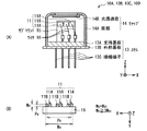
図1(A),(B)は、本技術の第1の実施の形態に係るプロジェクタ1の概略構成を表すものである。なお、プロジェクタ1が本技術の「投射型表示装置」の一具体例に相当する。図1(A)はプロジェクタ1を上から(y軸方向から)見たときの構成例を表し、図1(B)はプロジェクタ1を横から(x軸方向から)見たときの構成例を表す。図2(A),(B)は、図1のプロジェクタ1内の光路の一例を表すものである。図2(A)は、プロジェクタ1を上から(y軸方向から)見たときの光路の一例を表し、図2(B)はプロジェクタ1を横から(x軸方向から)見たときの光路の一例を表す。
<1. First Embodiment>
[Constitution]
1A and 1B show a schematic configuration of the
典型的には、y軸は垂直方向を向き、x軸は水平方向を向いているが、その逆に、y軸が水平方向を向き、x軸が垂直方向を向いていてもよい。なお、以下では、便宜的に、y軸は垂直方向を向き、x軸は水平方向を向いているものとして説明するものとする。また、以下において、「横方向」とはx軸方向を指しており、「縦方向」とはy軸方向を指しているものとする。 Typically, the y-axis faces the vertical direction and the x-axis faces the horizontal direction, but conversely, the y-axis may face the horizontal direction and the x-axis may face the vertical direction. In the following description, for the sake of convenience, the y-axis is oriented in the vertical direction and the x-axis is oriented in the horizontal direction. In the following description, it is assumed that “lateral direction” indicates the x-axis direction, and “vertical direction” indicates the y-axis direction.
プロジェクタ1は、例えば、照明光学系1A、空間変調素子60および投影光学系70を備えたものである。空間変調素子60は、入力された映像信号に基づいて照明光学系1Aからの光を変調することにより画像光を生成するものである。投影光学系70は、空間変調素子60で生成された画像光を反射型のスクリーン2に投射するものである。なお、照明光学系1Aが本技術の「照明装置」の一具体例に相当する。
The
照明光学系1Aは、空間変調素子60の照明範囲60A(被照射面)を照射する光束を供給するものである。なお、必要に応じて、照明光学系1Aの光が通過する領域上に、何らかの光学素子が設けられていてもよい。例えば、照明光学系1Aの光が通過する領域上に、照明光学系1Aからの光のうち可視光以外の光を減光するフィルタなどが設けられていてもよい。
The illumination
照明光学系1Aは、例えば、図1(A),(B)に示したように、光源10A,10B,10Cと、カップリングレンズ20A,20B,20Cと、光路合成素子30と、インテグレータ40と、コンデンサレンズ50と、微小振動素子100とを有している。なお、光源10Aが本技術の「第1の光源」の一具体例に相当し、光源10Bまたは光源10Cが本技術の「第2の光源」の一具体例に相当する。カップリングレンズ20Aが本技術の「第1の指向角変換素子」の一具体例に相当し、カップリングレンズ20Bまたはカップリングレンズ20Cが本技術の「第2の指向角変換素子」の一具体例に相当する。微小振動素子100が本技術の「第1の微小振動素子」の一具体例に相当する。
For example, as shown in FIGS. 1A and 1B, the illumination
光路合成素子30は、光源10A,10B,10Cからの光を合成するものであり、例えば、2つのダイクロイックミラー30A,30Bからなる。インテグレータ40は、照明範囲60Aにおける光の照度分布を均一化するものであり、例えば、一対のフライアイレンズ40A、40Bからなる。光源10Aの光軸上には、カップリングレンズ20Aと、光路合成素子30と、インテグレータ40と、コンデンサレンズ50とが光源10A側からこの順に配列されている。光源10Bの光軸は、光源10Aの光軸とダイクロイックミラー30Aにおいて直交しており、光源10Bの光軸上には、カップリングレンズ20Bおよびダイクロイックミラー30Aが光源10B側からこの順に配列されている。光源10Cの光軸は、光源10Aの光軸とダイクロイックミラー30Bにおいて直交しており、光源10Cの光軸上には、カップリングレンズ20Cおよびダイクロイックミラー30Bが光源10C側からこの順に配列されている。
The optical
なお、図1(A),(B)では、プロジェクタ1の各構成要素(光源10B,10C、カップリングレンズ20B,20Cを除く)がz軸と平行な線分上に配列されている場合が例示されているが、プロジェクタ1の各構成要素の一部がz軸と非平行な線分上に配列されていてもよい。例えば、図示しないが、照明光学系1A全体を図1(A),(B)の状態から90°回転させて照明光学系1Aの光軸がz軸と直交する方向を向くように照明光学系1Aがレイアウトされていてもよい。ただし、このようにした場合には、照明光学系1Aから出力された光を空間変調素子60に導く光学素子(例えばミラー)を設けることが必要である。また、例えば、光源10A、カップリングレンズ20Aおよび光路合成素子30を図1(A),(B)の状態から90°回転させて、これらの光軸をz軸と直交する方向を向くように光源10A、カップリングレンズ20Aおよび光路合成素子30がレイアウトされていてもよい。ただし、このようにした場合にも、光路合成素子30から出力された光をインテグレータ40に導く光学素子(例えばミラー)を設けることが必要である。
1A and 1B, each component of the projector 1 (except for the
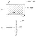
光源10A,10B,10Cは、それぞれ、例えば、図3(A),(B)〜図5(A),(B)に示したように、固体発光素子11と、固体発光素子11を支持するとともに覆うパッケージ12とを有している。固体発光素子11は、単一もしくは複数の点状、または単一もしくは複数の非点状の発光スポットからなる光射出領域から光を発するようになっている。固体発光素子11は、例えば、図3(A),(B)に示したように、所定の波長帯の光を発する単一のチップ11Aからなっていてもよいし、例えば、図4(A),(B)、図5(A),(B)に示したように、同一の波長帯もしくは互いに異なる波長帯の光を発する複数のチップ11Aからなっていてもよい。固体発光素子11が複数のチップ11Aからなる場合には、それらのチップ11Aは、例えば、図4(A),(B)に示したように、横方向に一列に配置されていたり、例えば、図5(A),(B)に示したように、横方向および縦方向に格子状に配置されていたりする。固体発光素子11に含まれるチップ11Aの数は、光源10A,10B,10Cごとに異なっていてもよいし、全ての光源10A,10B,10Cで互いに等しくなっていてもよい。
The
固体発光素子11が単一のチップ11Aからなる場合には、固体発光素子11としてのサイズ(WV×WH)は、例えば、図3(A)に示したように、単一のチップ11Aのサイズ(WV1×WH1)に等しい。一方、固体発光素子11が複数のチップ11Aからなる場合には、固体発光素子11としてのサイズは、例えば、図4(A),図5(A)に示したように、全てのチップ11Aをひとまとまりとしたときのサイズに等しい。複数のチップ11Aが横方向に一列に配置されている場合には、固体発光素子11としてのサイズ(WV×WH)は、図4(A)の例では、WV1×2WH1となる。また、複数のチップ11Aが、横方向および縦方向に格子状に配置されている場合には、固体発光素子11としてのサイズ(WV×WH)は、図5(A)の例では、2WV1×2WH1となる。
When the solid
チップ11Aは、発光ダイオード(LED)、有機EL発光素子(OLED)、またはレーザダイオード(LD)からなる。LEDおよびOLEDは無偏光の光であって、かつインコヒーレントな光を射出するものである。一方のLDは偏光光であって、かつコヒーレントな光(またはほぼコヒーレントな光)を射出するものである。
The
固体発光素子11が複数のチップ11Aからなる場合に、光源10A,10B,10Cのそれぞれに含まれるチップ11Aが全て、LDであってもよい。また、固体発光素子11が複数のチップ11Aからなる場合に、光源10A,10B,10Cのうち少なくとも1つの光源に含まれるチップ11AがLDであり、それ以外のチップ11AがLEDやOLEDであってもよい。
When the solid-state
固体発光素子11が複数のチップ11Aからなる場合に、固体発光素子11に含まれる各チップ11Aは、例えば、互いに同一の波長帯の光を発するようになっていてもよいし、互いに異なる波長帯の光を発するようになっていてもよい。各光源10A,10B,10Cに含まれるチップ11Aは、例えば、光源10A,10B,10Cごとに互いに異なる波長帯の光を発するようになっている。光源10Aに含まれるチップ11Aは、例えば、波長400nm〜500nm程度の波長の光(青色光)を発するものである。光源10Bに含まれるチップ11Aは、例えば、波長500nm〜600nm程度の波長の光(緑色光)を発するものである。光源10Cに含まれるチップ11Aは、例えば、波長600nm〜700nm程度の波長の光(赤色光)を発するものである。なお、光源10Aに含まれるチップ11Aが、青色光以外の光(緑色光または赤色光)を発するものであってもよい。また、光源10Bに含まれるチップ11Aが、緑色光以外の光(青色光または赤色光)を発するものであってもよい。また、光源10Cに含まれるチップ11Aが、赤色光以外の光(緑色光または青色光)を発するものであってもよい。
In the case where the solid
チップ11Aは、例えば、図3(A),(B)〜図6(A)〜(C)に示したように、チップ11Aサイズ(WV×WH)よりも小さなサイズ(PV1×PH1)の発光スポット11Bを有している。発光スポット11Bは、チップ11Aに電流を注入してチップ11Aを駆動したときにチップ11Aから光が発せられる領域(光射出領域)に相当する。チップ11AがLEDまたはOLEDである場合には、発光スポット11Bは非点状(面状)となるが、チップ11AがLDである場合には、発光スポット11BはLEDまたはOLEDの発光スポット11Bよりも小さな点状である。
The
固体発光素子11が単一のチップ11Aからなる場合には、発光スポット11Bの数は、例えば、図6(A)に示したように1つである。一方、固体発光素子11が複数のチップ11Aからなる場合には、発光スポット11Bの数は、例えば、図6(B),(C)に示したようにチップ11Aの数と等しい。ここで、固体発光素子11が単一のチップ11Aからなる場合には、固体発光素子11としての光射出領域のサイズ(PV×PH)は、発光スポット11Bのサイズ(PV1×PH1)に等しい。一方、固体発光素子11が複数のチップ11Aからなる場合には、固体発光素子11としての光射出領域のサイズ(PV×PH)は、最小面積で全てのチップ11Aの発光スポット11Bを囲ったときのその囲いのサイズに等しい。複数のチップ11Aが横方向に一列に配置されている場合には、光射出領域のサイズ(PV×PH)は、図6(B)の例では、PV1×2PH1よりも大きく、WV×WHよりも小さい。また、複数のチップ11Aが、横方向および縦方向に格子状に配置されている場合には、光射出領域のサイズ(PV×PH)は、図6(C)の例では、2PV1×2PH1よりも大きく、WV×WHよりも小さい。
When the solid
カップリングレンズ20Aは、例えば、図2(A),(B)に示したように、光源10Aから発せられた光を略平行光化するものであり、光源10Aから発せられた光の指向角(θH,θV)を、平行光の指向角と等しくなるように、またはそれに近づくように変換するものである。カップリングレンズ20Aは、光源10Aから発せられた光のうち指向角内の光が入射する位置に配置されている。カップリングレンズ20Bは、例えば、図2(A),(B)に示したように、光源10Bから発せられた光を略平行光化するものであり、光源10Bから発せられた光の指向角(θH,θV)を、平行光の指向角と等しくなるように、またはそれに近づくように変換するものである。カップリングレンズ20Bは、光源10Bから発せられた光のうち指向角内の光が入射する位置に配置されている。カップリングレンズ20Cは、例えば、図2(A),(B)に示したように、光源10Cから発せられた光を略平行光化するものであり、光源10Cから発せられた光の指向角(θH,θV)を、平行光の指向角と等しくなるように、またはそれに近づくように変換するものである。カップリングレンズ20Cは、光源10Cから発せられた光のうち指向角内の光が入射する位置に配置されている。つまり、カップリングレンズ20A,20B,20Cは、光源10A,10B,10Cごとに(パッケージごとに)1つずつ配置されている。なお、カップリングレンズ20A,20B,20Cは、それぞれ、単一のレンズによって構成されていてもよいし、複数のレンズによって構成されていてもよい。
For example, as shown in FIGS. 2A and 2B, the
ダイクロイックミラー30A,30Bは、波長選択性を持つ1枚のミラーを含むものである。なお、上記のミラーは、例えば、多層の干渉膜を蒸着して構成されたものである。ダイクロイックミラー30Aは、例えば、図2(A),(B)に示したように、ミラーの裏面側から入射した光(光源10A側から入射した光)をミラーの表面側に透過させるとともに、ミラーの表面側から入射した光(光源10B側から入射した光)をミラーで反射するようになっている。一方、ダイクロイックミラー30Bは、図2(A),(B)に示したように、ミラーの裏面側から入射した光(ダイクロイックミラー30A側から入射した光源10A,10Bの光)をミラーの表面側に透過させるとともに、ミラーの表面側から入射した光(光源10C側から入射した光)をミラーで反射するようになっている。従って、光路合成素子30は、光源10A,10B,10Cから発せられた個々の光束を単一の光束に合成するようになっている。
The
フライアイレンズ40A、40Bは、それぞれ、所定の配列状態(ここでは、縦×横=4×3のマトリクス状)に配置された複数のレンズ(セル)によって構成されたものである。フライアイレンズ40Bに含まれる複数のセル42は、フライアイレンズ40Aのセル41ごとに1つずつ対向して配置されている。フライアイレンズ40Aは、フライアイレンズ40Bの焦点位置(または略焦点位置)に配置されており、フライアイレンズ40Bは、フライアイレンズ40Aの焦点位置(または略焦点位置)に配置されている。従って、インテグレータ40は、フライアイレンズ40Aで分割形成された光束がフライアイレンズ40Bの像側のレンズ面近傍に焦点を結び、ここに2次光源面(光源像)を形成するようになっている。この2次光源面は投影光学系70の入射瞳と共役な面の位置に位置している。ただし、この2次光源面は、必ずしも厳密に投影光学系70の入射瞳と共役な面の位置に位置している必要はなく、設計上の許容範囲内に位置していればよい。フライアイレンズ40A、40Bは、一体に形成されたものであってもよい。
The fly-
一般に光源10A,10B,10Cから射出された光束は、その進行方向に垂直な面において不均一な強度分布をもっている。そのため、これら光束をそのまま照明範囲60A(被照射面)に導くと、照明範囲60Aでの照度分布が不均一になるが、上記のように光源10A,10B,10Cから射出された光束をインテグレータ40によって複数の光束に分割してそれぞれを照明範囲60Aに重畳的に導くようにすれば、照明範囲60A上の照度分布を均一にすることができる。
In general, light beams emitted from the
コンデンサレンズ50は、インテグレータ40により形成された多光源からの光束を集光して照明範囲60Aを重畳的に照明するものである。空間変調素子60は、光源10A,10B,10Cの各波長成分に対応した色画像信号に基づいて、照明光学系1Aからの光束を2次元的に変調し、これにより画像光を生成するものである。空間変調素子60は、例えば、図2(A),(B)に示したように、透過型の素子であり、例えば、透過型の液晶パネルによって構成されている。なお、図示しないが、空間変調素子60が反射型の素子、例えば、反射型の液晶パネルもしくはデジタルマイクロミラーデバイスによって構成されていてもよい。ただし、その場合には、空間変調素子60で反射された光が投影光学系70に入射するようになっていることが必要である。
The
微小振動素子100は、例えば、図1(A),(B)に示したように、光路合成素子30とインテグレータ40との間に配置されている。微小振動素子100は、照明範囲60Aにおける照明状態を時間的に変化させるものであり、例えば、図10に示したように、光学素子110と、光学素子110を微小振動させる駆動部120とを有している。光学素子110は、光源10A,10B,10C側から発せられた光が通過する領域に配置されている。駆動部120は、光路とは異なる箇所に配置されている。
For example, as shown in FIGS. 1A and 1B, the
光学素子110は、例えば、光射出側に傾斜面A1〜Anを有するプリズムアレイを含んで構成されている。プリズムアレイは、光源10A,10B,10C側から発せられた光を傾斜面A1〜Anごとに微小な光束L1〜Lnに分割するものである。
The optical element 110 is, for example, is configured to include a prism array having an inclined surface A 1 to A n on the light emission side. Prism array includes a
駆動部120は、光学素子110とインテグレータ40との相対位置を変位させるものである。駆動部120は、例えば、プリズムアレイの傾斜面A1〜Anの配列方向(図10の上下方向)に振動させることにより、光学素子110とインテグレータ40との相対位置を変位させるようになっている。これにより、インテグレータ40の入射面内において、光束L1〜Lnの入射位置が変化するので、照明領域60Aにおける照明状態を時間的に変化させることができる。なお、微小振動素子100による光束の走査は、連続周期的であってもよいし、離散的繰り返しであってもよい。いずれの場合であっても、照明領域60Aにおける照明状態を時間的に変化させることができる。また、光学素子110の傾斜面A1〜Anは、光束L1〜Lnのフライアイレンズ40Aへの入射角がフライアイレンズ40Aの許容角以内となるように構成されていることが好ましい。また、駆動部120は、光束L1〜Lnのフライアイレンズ40Aへの入射角がフライアイレンズ40Aの許容角以内となるように、微小振動素子100を振動させるようになっていることが好ましい。許容角とは、フライアイレンズ40B近傍に形成される各光源像がフライアイレンズ40Bに含まれる複数のセル42にまたがって形成されることのない、フライアイレンズ40Aへの入射角の最大値を指す。なお、許容角より大きな入射角で入射した光はフライアイレンズ40Aを透過しても照明範囲60Aを照明できないか、または、非常に低い効率でしか照明範囲60Aを照明できない。駆動部120は、小型化の容易な構成となっており、例えば、コイルおよび永久磁石(例えば、ネオジム(Nd)や鉄(Fe)、ホウ素(ボロン;B)等の材料からなる永久磁石)等を含んで構成されている。
The drive unit 120 is for displacing the relative position between the optical element 110 and the
次に、本実施の形態のプロジェクタ1の特徴部分について説明する。
Next, the characteristic part of the
(特徴部分その1)
本実施の形態では、フライアイレンズ40Aの各セル41によってフライアイレンズ40Bに形成される各光源像Sのサイズがフライアイレンズ40Bの1つのセル42のサイズを超えない大きさとなるように、カップリングレンズ20A,20B,20Cの焦点距離と、フライアイレンズ40A、40Bの焦点距離と、微小振動素子100の形状が設定されている。さらに、各光源像Sが、フライアイレンズ40Bの複数のセル42にまたがって形成されることがないように、微小振動素子100の振動振幅により光源像Sが変位する量が設定されている。
(Characteristic part 1)
In the present embodiment, the size of each light source image S formed on the fly-
これを式で表すと、以下のようになる。
h1+d1=P1×(fFEL/fCL1)+d1≦hFEL2…(1)
h2+d2=P2×(fFEL/fCL2)+d2≦hFEL2…(2)
h3+d3=P3×(fFEL/fCL3)+d3≦hFEL2…(3)
h1:光源10Aの光によって形成される光源像S(光源像S1)のサイズ
h2:光源10Bの光によって形成される光源像S(光源像S2)のサイズ
h3:光源10Cの光によって形成される光源像S(光源像S3)のサイズ
P1:光源10Aに含まれる固体発光素子11の光射出領域のサイズ
P2:光源10Bに含まれる固体発光素子11の光射出領域のサイズ
P3:光源10Cに含まれる固体発光素子11の光射出領域のサイズ
fFEL:フライアイレンズ40A,40Bの焦点距離
fCL1:カップリングレンズ20Aの焦点距離
fCL2:カップリングレンズ20Bの焦点距離
fCL3:カップリングレンズ20Cの焦点距離
hFEL2:フライアイレンズ40Bの1つのセル42のサイズ
d1:微小振動素子100の振動振幅により光源像S1が変位する量
d2:微小振動素子100の振動振幅により光源像S2が変位する量
d3:微小振動素子100の振動振幅により光源像S3が変位する量
This is expressed as follows.
h 1 + d 1 = P 1 × (f FEL / f CL1 ) + d 1 ≦ h FEL2 (1)
h 2 + d 2 = P 2 × (f FEL / f CL2 ) + d 2 ≦ h FEL2 (2)
h 3 + d 3 = P 3 × (f FEL / f CL3 ) + d 3 ≦ h FEL2 (3)
h 1 : size of light source image S (light source image S 1 ) formed by light from
なお、光源10Aに含まれる固体発光素子11が単一のチップ11Aからなる場合には、P1は、そのチップ11Aの発光スポット11Bのサイズに等しい。同様に、光源10Bに含まれる固体発光素子11が単一のチップ11Aからなる場合には、P2は、そのチップ11Aの発光スポット11Bのサイズに等しく、光源10Cに含まれる固体発光素子11が単一のチップ11Aからなる場合には、P3は、そのチップ11Aの発光スポット11Bのサイズに等しい。光源10Aに含まれる固体発光素子11が複数のチップ11Aからなる場合には、P1は、最小面積で全てのチップ11Aの発光スポット11Bを囲ったときのその囲いのサイズに等しい。同様に、光源10Bに含まれる固体発光素子11が複数のチップ11Aからなる場合には、P2は、最小面積で全てのチップ11Aの発光スポット11Bを囲ったときのその囲いのサイズに等しい。光源10Cに含まれる固体発光素子11が複数のチップ11Aからなる場合には、P3は、最小面積で全てのチップ11Aの発光スポット11Bを囲ったときのその囲いのサイズに等しい。また、カップリングレンズ20Aが複数のレンズによって構成されている場合には、fCL1は、各レンズの合成焦点距離とする。同様に、カップリングレンズ20Bが複数のレンズによって構成されている場合には、fCL2は、各レンズの合成焦点距離とする。カップリングレンズ20Cが複数のレンズによって構成されている場合には、fCL3は、各レンズの合成焦点距離とする。
In the case where the solid-state light-emitting
上記の式(1)〜(3)とおおよそ等価な式として、以下の式(4)〜(6)を挙げることができる。式(4)〜(6)は、固体発光素子11の光射出領域のサイズが固体発光素子11のサイズと概ね等しい場合に特に有益である。
h1+d1=W1×(fFEL/fCL1)+d1≦hFEL2…(4)
h2+d2=W2×(fFEL/fCL2)+d2≦hFEL2…(5)
h3+d3=W3×(fFEL/fCL3)+d3≦hFEL2…(6)
W1:光源10Aに含まれる固体発光素子11のサイズ
W2:光源10Bに含まれる固体発光素子11のサイズ
W3:光源10Cに含まれる固体発光素子11のサイズ
The following expressions (4) to (6) can be given as expressions approximately equivalent to the above expressions (1) to (3). Expressions (4) to (6) are particularly useful when the size of the light emission region of the solid state light emitting
h 1 + d 1 = W 1 × (f FEL / f CL1 ) + d 1 ≦ h FEL2 (4)
h 2 + d 2 = W 2 × (f FEL / f CL2 ) + d 2 ≦ h FEL2 (5)
h 3 + d 3 = W 3 × (f FEL / f CL3 ) + d 3 ≦ h FEL2 (6)
W 1 : Size of the solid state
なお、固体発光素子11が単一のチップ11Aからなる場合には、Wは、そのチップ11Aのサイズに等しい。また、固体発光素子11が複数のチップ11Aからなる場合には、Wは、全てのチップ11Aを単一のチップとしてみたときの、そのチップのサイズに等しい。
In the case where the solid
ところで、本実施の形態において、例えば、図7(A),(B)に示したように、フライアイレンズ40A,40Bの各セル41,42が1以外の縦横比(アスペクト比)を有している場合には、カップリングレンズ20A,20B,20Cの焦点距離と、フライアイレンズ40A、40Bの焦点距離とが以下の6つの関係式を満たしていることが好ましい。このとき、微小振動素子100は、フライアイレンズ40A,40Bの各セル41,42の長手方向および短手方向のうち少なくとも長手方向に振幅成分を有する振動をするようになっていることが好ましい。さらに、カップリングレンズ20A,20B,20Cの縦横の焦点距離の比(fCL1H/fCL1V,fCL2H/fCL2V,fCL3H/fCL3V)(アナモフィック比)と、フライアイレンズ40Bの各セル42のサイズの縦横比の逆数(hFEL2V/hFEL2H)とを互いに等しくし、照明光学系1Aをアナモフィック光学系とすることがより好ましい。例えば、フライアイレンズ40Bの各セル42が第1の方向(例えば横方向)に長い形状となっている場合には、カップリングレンズ20A,20B,20Cとして、焦点距離fCL1V,fCL2V,fCL3Vが焦点距離fCL1H,fCL2H,fCL3Hよりも長いものを用いる。以下の式(7)〜(12)を模式的に表すと、図9(A)〜(C)のようになる。ここで、図9(A)は、微小振動素子100の振動により光源像S(光源像S1,S2,S3)が第1の方向(例えば横方向)またはそれに対応する方向に振動している様子を表したものである。図9(B)は、微小振動素子100の振動により光源像S(光源像S1,S2,S3)が第2の方向(例えば縦方向)またはそれに対応する方向に振動している様子を表したものである。図9(C)は、微小振動素子100の振動により光源像S(光源像S1,S2,S3)が第1の方向および第2の方向を含む面内で振動している様子を表したものである。
h1H+d1H=P1H×(fFELH/fCL1H)+d1H≦hFEL2H…(7)
h2H+d2H=P2H×(fFELH/fCL2H)+d2H≦hFEL2H…(8)
h3H+d3H=P3H×(fFELH/fCL3H)+d3H≦hFEL2H…(9)
h1V+d1V=P1V×(fFELV/fCL1V)+d1V≦hFEL2V…(10)
h2V+d2V=P2V×(fFELV/fCL2V)+d2V≦hFEL2V…(11)
h3V+d3V=P3V×(fFELV/fCL3V)+d3V≦hFEL2V…(12)
h1H:光源10Aの光によって形成される光源像S(光源像S1)の第1の方向(例えば横方向)のサイズ
h2H:光源10Bの光によって形成される光源像S(光源像S2)の第1の方向(例えば横方向)のサイズ
h3H:光源10Cの光によって形成される光源像S(光源像S3)の第1の方向(例えば横方向)のサイズ
h1V:光源10Aの光によって形成される光源像S(光源像S1)の、第1の方向と直交する第2の方向(例えば縦方向)のサイズ
h2V:光源10Bの光によって形成される光源像S(光源像S2)の、第1の方向と直交する第2の方向(例えば縦方向)のサイズ
h3V:光源10Cの光によって形成される光源像S(光源像S3)の、第1の方向と直交する第2の方向(例えば縦方向)のサイズ
P1H:光源10Aに含まれる固体発光素子11の光射出領域の、第1の方向またはそれに対応する方向のサイズ
P2H:光源10Bに含まれる固体発光素子11の光射出領域の、第1の方向またはそれに対応する方向のサイズ
P3H:光源10Cに含まれる固体発光素子11の光射出領域の、第1の方向またはそれに対応する方向のサイズ
P1V:光源10Aに含まれる固体発光素子11の光射出領域の、第2の方向またはそれに対応する方向のサイズ
P2V:光源10Bに含まれる固体発光素子11の光射出領域の、第2の方向またはそれに対応する方向のサイズ
P3V:光源10Cに含まれる固体発光素子11の光射出領域の、第2の方向またはそれに対応する方向のサイズ
fFELH:フライアイレンズ40A,40Bの第1の方向の焦点距離
fFELV:フライアイレンズ40A,40Bの第2の方向の焦点距離
fCL1H:カップリングレンズ20Aの、第1の方向またはそれに対応する方向の焦点距離
fCL2H:カップリングレンズ20Bの、第1の方向またはそれに対応する方向の焦点距離
fCL3H:カップリングレンズ20Cの、第1の方向またはそれに対応する方向の焦点距離
fCL1V:カップリングレンズ20Aの、第2の方向またはそれに対応する方向の焦点距離
fCL2V:カップリングレンズ20Bの、第2の方向またはそれに対応する方向の焦点距離
fCL3V:カップリングレンズ20Cの、第2の方向またはそれに対応する方向の焦点距離
hFEL2H:フライアイレンズ40Bの1つのセル42の第1の方向のサイズ
hFEL2V:フライアイレンズ40Bの1つのセル42の第2の方向のサイズ
d1H:微小振動素子100の振動振幅により光源像S1が変位する量のうち、第1の方向またはそれに対応する方向の成分(d1H≧0、ただしd1V=0のときはd1H>0)
d2H:微小振動素子100の振動振幅により光源像S2が変位する量のうち、第1の方向またはそれに対応する方向の成分(d2H≧0、ただしd2V=0のときはd2H>0)
d3H:微小振動素子100の振動振幅により光源像S3が変位する量のうち、第1の方向またはそれに対応する方向の成分(d3H≧0、ただしd3V=0のときはd3H>0)
d1V:微小振動素子100の振動振幅により光源像S1が変位する量のうち、第2の方向またはそれに対応する方向の成分(d1V≧0、ただしd1H=0のときはd1V>0)
d2V:微小振動素子100の振動振幅により光源像S2が変位する量のうち、第2の方向またはそれに対応する方向の成分(d2V≧0、ただしd2H=0のときはd2V>0)
d3V:微小振動素子100の振動振幅により光源像S3が変位する量のうち、第2の方向またはそれに対応する方向の成分(d3V≧0、ただしd3H=0のときはd3V>0)
By the way, in this embodiment, for example, as shown in FIGS. 7A and 7B, the
h 1H + d 1H = P 1H × (f FELH / f CL1H ) + d 1H ≦ h FEL2H (7)
h 2H + d 2H = P 2H × (f FELH / f CL2H ) + d 2H ≦ h FEL2H (8)
h 3H + d 3H = P 3H × (f FELH / f CL3H ) + d 3H ≦ h FEL2H (9)
h 1V + d 1V = P 1V × (f FELV / f CL1V) + d 1V ≦ h FEL2V ... (10)
h 2V + d 2V = P 2V × (f FELV / f CL2V ) + d 2V ≦ h FEL2V (11)
h 3V + d 3V = P 3V × (f FELV / f CL3V) + d 3V ≦ h FEL2V ... (12)
h 1H : Size of light source image S (light source image S 1 ) formed in the first direction (for example, in the horizontal direction) formed by light from light source 10A h 2H : Light source image S (light source image S formed by light from light source 10B) 2 ) size in the first direction (for example, lateral direction) h 3H : size in the first direction (for example, lateral direction) of the light source image S (light source image S 3 ) formed by the light of the light source 10C h 1V : light source Size h 2V of light source image S (light source image S 1 ) formed by light of 10A in a second direction (eg, vertical direction) orthogonal to the first direction: light source image S formed by light of light source 10B Size of (light source image S 2 ) in a second direction (for example, vertical direction) orthogonal to the first direction h 3V : first of light source image S (light source image S 3 ) formed by light from light source 10C Size P 1H in the second direction (eg, the vertical direction) orthogonal to the direction of the light source 10A The size of the light emission region of the solid light emitting element 11 included in the first direction or the direction corresponding thereto P 2H : the first direction of the light emission region of the solid light emitting element 11 included in the light source 10B or corresponding to it. Direction size P 3H : Size of light emission area of solid-state light emitting element 11 included in light source 10C in the first direction or a direction corresponding thereto P 1V : Size of light emission area of solid-state light emitting element 11 included in light source 10A Size P 2V in the second direction or a direction corresponding thereto P 2V : Size in the second direction or a direction corresponding thereto in the light emission region of the solid-state light emitting element 11 included in the light source 10B P 3V : Solid light emission included in the light source 10C light emission region of the element 11, the second direction or in the corresponding direction size f FELH: the fly-eye lens 40A, the first direction 40B focal length f FELV: fly Irenzu 40A, 40B in the second direction focal length f CL1H: a coupling lens 20A, a first direction or in the corresponding direction of the focal length f CL2H: a coupling lens 20B, corresponding to a first direction or Focal length of direction f CL3H : Focal length of coupling lens 20C in the first direction or a direction corresponding thereto f CL1V : Focal length of coupling lens 20A in the second direction or a direction corresponding thereto f CL2V : Cup Focal length of ring lens 20B in the second direction or a direction corresponding thereto f CL3V : Focal length of coupling lens 20C in the second direction or a direction corresponding thereto h FEL2H : One cell 42 of fly-eye lens 40B H FEL2V : Size of one cell 42 of the fly-eye lens 40B in the second direction d 1H : Of the amount of displacement of the light source image S 1 due to the vibration amplitude of the micro-vibration element 100, the component in the first direction or the corresponding direction (d 1H ≧ 0, where d 1H > 0 when d 1V = 0. )
d 2H: Of the amount of the light source images S 2 is displaced by the vibration amplitude of the
d 3H: Of the amount of the light source images S 3 is displaced by the vibration amplitude of the
d 1V: Of the amount of the light source images S 1 is displaced by the vibration amplitude of the
d 2V: Of the amount of the light source images S 2 is displaced by the vibration amplitude of the
d 3V: Of the amount of the light source images S 3 is displaced by the vibration amplitude of the
ここで、「第1の方向またはそれに対応する方向」は、光源10A,10B,10C、カップリングレンズ20A,20B,20Cがインテグレータ40の光軸上に配置されている場合には第1の方向を指している。また、「第1の方向またはそれに対応する方向」は、光源10A,10B,10C、カップリングレンズ20A,20B,20Cがインテグレータ40の光軸から外れた光路上に配置されている場合には、光源10A,10B,10Cからインテグレータ40までの光路上に配置された光学素子のレイアウトの関係から第1の方向に対応する方向を指している。
Here, the “first direction or the direction corresponding thereto” is the first direction when the
また、「第2の方向またはそれに対応する方向」は、光源10A,10B,10C、カップリングレンズ20A,20B,20Cがインテグレータ40の光軸上に配置されている場合には第2の方向を指している。また、「第2の方向またはそれに対応する方向」は、光源10A,10B,10C、カップリングレンズ20A,20B,20Cがインテグレータ40の光軸から外れた光路上に配置されている場合には、光源10A,10B,10Cからインテグレータ40までの光路上に配置された光学素子のレイアウトの関係から第2の方向に対応する方向を指している。
The “second direction or a direction corresponding to the second direction” is the second direction when the
なお、光源10Aに含まれる固体発光素子11が単一のチップ11Aからなる場合には、P1Hは、そのチップ11Aの発光スポット11Bの第1の方向またはそれに対応する方向のサイズに等しい。同様に、光源10Bに含まれる固体発光素子11が単一のチップ11Aからなる場合には、P2Hは、そのチップ11Aの発光スポット11Bの第1の方向またはそれに対応する方向のサイズに等しい。光源10Cに含まれる固体発光素子11が単一のチップ11Aからなる場合には、P3Hは、そのチップ11Aの発光スポット11Bの第1の方向またはそれに対応する方向のサイズに等しい。また、光源10Aに含まれる固体発光素子11が複数のチップ11Aからなる場合には、P1Hは、最小面積で全てのチップ11Aの発光スポット11Bを囲ったときのその囲いの、第1の方向またはそれに対応する方向のサイズに等しい。同様に、光源10Bに含まれる固体発光素子11が複数のチップ11Aからなる場合には、P2Hは、最小面積で全てのチップ11Aの発光スポット11Bを囲ったときのその囲いの、第1の方向またはそれに対応する方向のサイズに等しい。光源10Cに含まれる固体発光素子11が複数のチップ11Aからなる場合には、P3Hは、最小面積で全てのチップ11Aの発光スポット11Bを囲ったときのその囲いの、第1の方向またはそれに対応する方向のサイズに等しい。一方、光源10Aに含まれる固体発光素子11が単一のチップ11Aからなる場合には、P1Vは、そのチップ11Aの発光スポット11Bの第2の方向またはそれに対応する方向のサイズに等しい。同様に、光源10Bに含まれる固体発光素子11が単一のチップ11Aからなる場合には、P2Vは、そのチップ11Aの発光スポット11Bの第2の方向またはそれに対応する方向のサイズに等しい。光源10Cに含まれる固体発光素子11が単一のチップ11Aからなる場合には、P3Vは、そのチップ11Aの発光スポット11Bの第2の方向またはそれに対応する方向のサイズに等しい。また、光源10Aに含まれる固体発光素子11が複数のチップ11Aからなる場合には、P1Vは、最小面積で全てのチップ11Aの発光スポット11Bを囲ったときのその囲いの、第2の方向またはそれに対応する方向のサイズに等しい。同様に、光源10Bに含まれる固体発光素子11が複数のチップ11Aからなる場合には、P2Vは、最小面積で全てのチップ11Aの発光スポット11Bを囲ったときのその囲いの、第2の方向またはそれに対応する方向のサイズに等しい。光源10Cに含まれる固体発光素子11が複数のチップ11Aからなる場合には、P3Vは、最小面積で全てのチップ11Aの発光スポット11Bを囲ったときのその囲いの、第2の方向またはそれに対応する方向のサイズに等しい。
When the solid
また、本実施の形態において、フライアイレンズ40A,40Bの各セル41,42が1以外の縦横比を有している場合には、フライアイレンズ40Aの各セル41のサイズの縦横比と、照明範囲60Aの縦横比とが以下の関係式を満たしていることが好ましい。ここで、照明範囲60Aの縦横比H/V(図8)は、空間変調素子60の解像度と相関を有しており、例えば、空間変調素子60の解像度がVGA(640×480)である場合には640/480となっており、例えば、空間変調素子60の解像度がWVGA(800×480)である場合には800/480となっている。
hFEL1H/hFEL1V=H/V…(13)
hFEL1H:フライアイレンズ40Aの1セルの第1の方向のサイズ
hFEL1V:フライアイレンズ40Aの1セルの第2の方向のサイズ
H:照明範囲60Aの第1の方向のサイズ
V:照明範囲60Aの第2の方向のサイズ
In the present embodiment, when the
h FEL1H / h FEL1V = H / V (13)
h FEL1H : size in the first direction of one cell of the fly-
(特徴部分その2)
また、本実施の形態では、カップリングレンズ20A,20B,20Cに入射する光のビームサイズが20A,20B,20Cのサイズを超えない大きさとなるように、カップリングレンズ20A,20B,20Cの焦点距離および開口数が設定されている。これを式で表すと、以下のようになる。
φCL1=2×fCL1×NA1≦hCL1…(14)
φCL2=2×fCL2×NA2≦hCL2…(15)
φCL3=2×fCL3×NA3≦hCL3…(16)
φCL1:カップリングレンズ20Aに入射する光のビームサイズ
φCL2:カップリングレンズ20Bに入射する光のビームサイズ
φCL3:カップリングレンズ20Cに入射する光のビームサイズ
NA1:カップリングレンズ20Aの開口数
NA2:カップリングレンズ20Bの開口数
NA3:カップリングレンズ20Cの開口数
hCL1:カップリングレンズ20Aのサイズ
hCL2:カップリングレンズ20Bのサイズ
hCL3:カップリングレンズ20Cのサイズ
(Characteristic part 2)
In the present embodiment, the focal points of the
φ CL1 = 2 × f CL1 × NA 1 ≦ h CL1 (14)
φ CL2 = 2 × f CL2 × NA 2 ≦ h CL2 (15)
φ CL3 = 2 × f CL3 × NA 3 ≦ h CL3 (16)
φ CL1 : beam size of light incident on the
ところで、本実施の形態において、カップリングレンズ20A,20B,20Cが1以外の縦横比(アスペクト比)を有している場合には、カップリングレンズ20A,20B,20Cの焦点距離および開口数が以下の6つの関係式を満たしていることが好ましい。
φCL1H=2×fCL1H×NA1H≦hCL1H…(17)
φCL2H=2×fCL2H×NA2H≦hCL2H…(18)
φCL3H=2×fCL3H×NA3H≦hCL3H…(19)
φCL1V=2×fCL1V×NA1V≦hCL1V…(20)
φCL2V=2×fCL2V×NA2V≦hCL2V…(21)
φCL3V=2×fCL3V×NA3V≦hCL3V…(22)
φCL1H:カップリングレンズ20Aに入射する光の、第3の方向(カップリングレンズ20Aの短手方向またはそれに対応する方向)のビームサイズ
φCL2H:カップリングレンズ20Bに入射する光の、第5の方向(カップリングレンズ20Bの短手方向またはそれに対応する方向)のビームサイズ
φCL3H:カップリングレンズ20Cに入射する光の、第7の方向(カップリングレンズ20Cの短手方向またはそれに対応する方向)のビームサイズ
φCL1V:カップリングレンズ20Aに入射する光の、第3の方向と直交する第4の方向(カップリングレンズ20Aの長手方向またはそれに対応する方向)のビームサイズ
φCL2V:カップリングレンズ20Bに入射する光の、第5の方向と直交する第6の方向(カップリングレンズ20Bの長手方向またはそれに対応する方向)のビームサイズ
φCL3V:カップリングレンズ20Cに入射する光の、第7の方向と直交する第8の方向(カップリングレンズ20Cの長手方向またはそれに対応する方向)のビームサイズ
NA1H:カップリングレンズ20Aの、第3の方向の開口数
NA2H:カップリングレンズ20Bの、第5の方向の開口数
NA3H:カップリングレンズ20Cの、第7の方向の開口数
NA1V:カップリングレンズ20Aの、第4の方向の開口数
NA2V:カップリングレンズ20Bの、第6の方向の開口数
NA3V:カップリングレンズ20Cの、第8の方向の開口数
hCL1H:カップリングレンズ20Aの、第3の方向のサイズ
hCL2H:カップリングレンズ20Bの、第5の方向のサイズ
hCL3H:カップリングレンズ20Cの、第7の方向のサイズ
hCL1V:カップリングレンズ20Aの、第4の方向のサイズ
hCL2V:カップリングレンズ20Bの、第6の方向のサイズ
hCL3V:カップリングレンズ20Cの、第8の方向のサイズ
In the present embodiment, when the
φ CL1H = 2 × f CL1H × NA 1H ≦ h CL1H (17)
φ CL2H = 2 × f CL2H × NA 2H ≦ h CL2H (18)
φ CL3H = 2 × f CL3H × NA 3H ≦ h CL3H (19)
φ CL1V = 2 × f CL1V × NA 1V ≦ h CL1V (20)
φ CL2V = 2 × f CL2V × NA 2V ≦ h CL2V (21)
φ CL3V = 2 × f CL3V × NA 3V ≦ h CL3V (22)
φ CL1H : Beam size of the light incident on the
なお、第3の方向が、第1の方向(例えば横方向)またはそれに対応する方向であることが好ましい。第4の方向が、第2の方向(例えば縦方向)またはそれに対応する方向であることが好ましい。第5の方向が、第1の方向(例えば横方向)またはそれに対応する方向であることが好ましい。第6の方向が、第2の方向(例えば縦方向)またはそれに対応する方向であることが好ましい。第7の方向が、第1の方向(例えば横方向)またはそれに対応する方向であることが好ましい。第8の方向が、第2の方向(例えば縦方向)またはそれに対応する方向であることが好ましい。 The third direction is preferably the first direction (for example, the lateral direction) or a direction corresponding thereto. It is preferable that the fourth direction is a second direction (for example, a vertical direction) or a direction corresponding thereto. The fifth direction is preferably the first direction (for example, the lateral direction) or a direction corresponding thereto. The sixth direction is preferably the second direction (for example, the vertical direction) or a direction corresponding thereto. The seventh direction is preferably the first direction (for example, the lateral direction) or a direction corresponding thereto. It is preferable that the eighth direction is the second direction (for example, the vertical direction) or a direction corresponding to the second direction.
[作用・効果]
次に、本実施の形態のプロジェクタ1の作用・効果について説明する。本実施の形態では、インテグレータ40を透過した光が照明する照明範囲60Aにおける照明状態を時間的に変化させる微小振動素子100が、光路合成素子30とインテグレータ40との間に設けられている。これにより、スペックルを人間の眼の中で気にならない程度に平均化することが可能となる。また、本実施の形態では、フライアイレンズ40Aの各セル41によってフライアイレンズ40Bに形成される各光源像Sのサイズがフライアイレンズ40Bの1つのセル42のサイズを超えない大きさとなるように、カップリングレンズ20A,20B,20Cの焦点距離fCL1,fCL2,fCL3と、フライアイレンズ40A,40Bの焦点距離fFELと、微小振動素子100の形状が設定されている。さらに、各光源像Sが、フライアイレンズ40Bの複数のセル42にまたがって形成されることがないように、微小振動素子100の振動振幅により光源像Sが変位する量が設定されている。これにより、フライアイレンズ40Bに入射した光が効率良く照明範囲60Aにまで到達する。なお、微小振動素子100は照明範囲60Aにおける照明状態を時間的に変化させることができる程度に振動するだけなので、微小振動素子100が照明光学系1Aの小型化を阻害することはない。以上のことから、本実施の形態では、小型化および光の利用効率向上を図りつつ、スペックルの発生を低減することができる。
[Action / Effect]
Next, functions and effects of the
また、本実施の形態において、フライアイレンズ40A,40Bの各セルが1以外の縦横比を有している場合に、その縦横比を考慮して、カップリングレンズ20A,20B,20Cの焦点距離fCL1H,fCL2H,fCL3H,fCL1V,fCL2V,fCL3Vと、フライアイレンズ40A,40Bの焦点距離fFELH,fFELVとを設定するようにした場合には、照明光学系1Aにおける光利用効率をさらに改善することができる。また、本実施の形態において、カップリングレンズ20A,20B,20Cが1以外の縦横比を有している場合に、その縦横比を考慮して、カップリングレンズ20A,20B,20Cの焦点距離fCL1H,fCL2H,fCL3H,fCL1V,fCL2V,fCL3Vおよび開口数NA1H,NA2H,NA3H,NA1V,NA2V,NA3Vを設定するようにした場合には、照明光学系1Aにおける光利用効率をさらに改善することができる。また、本実施の形態において、光源10A,10B,10Cの指向角がそれぞれ異なる場合に、それぞれの指向角を考慮して、カップリングレンズ20A,20B,20Cの焦点距離fCL1H,fCL2H,fCL3H,fCL1V,fCL2V,fCL3Vおよび開口数NA1H,NA2H,NA3H,NA1V,NA2V,NA3Vをそれぞれ設定するようにした場合には、照明光学系1Aにおける光利用効率をさらに改善することができる。
Further, in the present embodiment, when each cell of the fly-
上記実施の形態において、LDからなるチップ11Aが光源10Aだけに含まれており、それ以外の光源(光源10B,10C)には含まれていない場合には、例えば、図11に示したように、微小振動素子100が光源10Aとカップリングレンズ20Aとの間に設けられていてもよい。また、例えば、図12に示したように、微小振動素子100がカップリングレンズ20Aと光路合成素子30との間に設けられていてもよい。また、上記実施の形態において、LDからなるチップ11Aが光源10A,10Bだけに含まれており、それ以外の光源(光源10C)には含まれていない場合には、図示しないが、微小振動素子100が光源10Aとカップリングレンズ20Aとの間に設けられるとともに、光源10Bとカップリングレンズ20Bとの間に設けられていてもよい。このとき、光源10Aとカップリングレンズ20Aとの間に設けられた微小振動素子100が本技術の「第1の微小振動素子」の一具体例に相当し、光源10Bとカップリングレンズ20Bとの間に設けられた微小振動素子100が本技術の「第2の微小振動素子」の一具体例に相当する。また、上記実施の形態において、LDからなるチップ11Aが光源10A,10B,10Cの全てに含まれている場合に、図示しないが、微小振動素子100が、光源10Aとカップリングレンズ20Aとの間、光源10Bとカップリングレンズ20Bとの間、さらに光源10Cとカップリングレンズ20Cとの間に設けられていてもよい。このとき、光源10Aとカップリングレンズ20Aとの間に設けられた微小振動素子100が本技術の「第1の微小振動素子」の一具体例に相当する。また、光源10Bとカップリングレンズ20Bとの間に設けられた微小振動素子100、または光源10Cとカップリングレンズ20Cとの間に設けられた微小振動素子100が本技術の「第2の微小振動素子」の一具体例に相当する。なお、本技術の「第2の微小振動素子」の一具体例に相当する微小振動素子100の構成は、光源10Aとカップリングレンズ20Aとの間に設けられた微小振動素子100の構成と同様である。
In the above embodiment, when the
<2.第2の実施の形態>
[構成]
図13(A),(B)は、本技術の第2の実施の形態に係るプロジェクタ3の概略構成を表すものである。なお、プロジェクタ3が本技術の「投射型表示装置」の一具体例に相当する。図13(A)はプロジェクタ3を上から(y軸方向から)見たときの構成例を表し、図13(B)はプロジェクタ3を横から(x軸方向から)見たときの構成例を表す。図14(A),(B)は、図13のプロジェクタ3内の光路の一例を表すものである。図14(A)は、プロジェクタ3を上から(y軸方向から)見たときの光路の一例を表し、図14(B)はプロジェクタ3を横から(x軸方向から)見たときの光路の一例を表す。
<2. Second Embodiment>
[Constitution]
13A and 13B show a schematic configuration of the
プロジェクタ3は、照明光学系3Aを備えている点で、照明光学系1Aを備えたプロジェクタ1の構成と相違する。そこで、以下では、プロジェクタ1との相違点について主に説明、プロジェクタ1との共通点についての説明を適宜省略するものとする。
The
照明光学系3Aでは、照明光学系1Aのカップリングレンズ20A,20B,20Cと、ダイクロイックミラー30A,30Bとが省略され、その代わりに、カップリングレンズ20Dと、ダイクロイックミラー30Cとが設けられている。ダイクロイックミラー30Cは、光源10A,10B,10Cのそれぞれの光軸が互いに交差する箇所に配置されている。カップリングレンズ20Dは、ダイクロイックミラー30Cの光射出側に配置されており、ダイクロイックミラー30Cとインテグレータ40との間に配置されている。微小振動素子100は、カップリングレンズ20Dとインテグレータ40との間に配置されている。
In the illumination
ダイクロイックミラー30Cは、波長選択性を持つ2枚のミラーを含むものである。なお、上記のミラーは、例えば、多層の干渉膜を蒸着して構成されたものである。2枚のミラーは互いに直交して配置されており、ミラーの表面がダイクロイックミラー30Cの光射出側を向くように配置されている。ダイクロイックミラー30Cは、例えば、図14(A)に示したように、一方のミラー(以下、便宜的にミラーAと称する)の裏面側から入射した光(光源10A,10B側から入射した光)をミラーAの表面側に透過させるとともに、ミラーAの表面側から入射した光(光源10C側から入射した光)をミラーAで反射するようになっている。また、ダイクロイックミラー30Cは、例えば、図14(A)に示したように、他方のミラー(以下、便宜的にミラーBと称する)の裏面側から入射した光(光源10A,10C側から入射した光)をミラーBの表面側に透過させるとともに、ミラーBの表面側から入射した光(光源10B側から入射した光)をミラーBで反射するようになっている。従って、光路合成素子30は、光源10A,10B,10Cから発せられた個々の光束を単一の光束に合成するようになっている。
The
カップリングレンズ20Dは、例えば、図14(A),(B)に示したように、ダイクロイックミラー30C側から入射してきた光を略平行光化するものであり、ダイクロイックミラー30C側から入射してきた光の指向角を、平行光の指向角と等しくなるように、またはそれに近づくように変換するものである。
For example, as illustrated in FIGS. 14A and 14B, the coupling lens 20 </ b> D converts light incident from the
[作用・効果]
次に、本実施の形態のプロジェクタ3の作用・効果について説明する。本実施の形態では、インテグレータ40を透過した光が照明する照明範囲60Aにおける照明状態を時間的に変化させる微小振動素子100が、カップリングレンズ20Dとインテグレータ40との間に設けられている。これにより、スペックルを人間の眼の中で気にならない程度に平均化することが可能となる。また、本実施の形態では、フライアイレンズ40Aの各セル41によってフライアイレンズ40Bに形成される各光源像Sのサイズがフライアイレンズ40Bの1つのセル42のサイズを超えない大きさとなるように、カップリングレンズ20Dの焦点距離fCL4と、フライアイレンズ40A,40Bの焦点距離fFELと、微小振動素子100の形状が設定されている。さらに、各光源像Sが、フライアイレンズ40Bの複数のセル42にまたがって形成されることがないように、微小振動素子100の振動振幅により光源像Sが変位する量が設定されている。これにより、フライアイレンズ40Bに入射した光が効率良く照明範囲60Aにまで到達する。なお、微小振動素子100は照明範囲60Aにおける照明状態を時間的に変化させることができる程度に振動するだけなので、微小振動素子100が照明光学系3Aの小型化を阻害することはない。以上のことから、本実施の形態では、小型化および光の利用効率向上を図りつつ、スペックルの発生を低減することができる。
[Action / Effect]
Next, operations and effects of the
また、本実施の形態において、フライアイレンズ40A,40Bの各セルが1以外の縦横比を有している場合に、その縦横比を考慮して、カップリングレンズ20Dの焦点距離fCL4H,fCL4Vと、フライアイレンズ40A,40Bの焦点距離fFELH,fFELVとを設定するようにした場合には、照明光学系3Aにおける光利用効率をさらに改善することができる。また、本実施の形態において、カップリングレンズ20Dが1以外の縦横比を有している場合に、その縦横比を考慮して、カップリングレンズ20Dの焦点距離fCL4H,fCL4Vおよび開口数NA4H,NA4Vを設定するようにした場合には、照明光学系3Aにおける光利用効率をさらに改善することができる。
In the present embodiment, when each cell of the fly-
なお、本実施の形態では、第1の実施の形態のfCL1,fCL2,fCL3が、カップリングレンズ20Dの焦点距離fCL4となる。同様に、第1の実施の形態のfCL1H,fCL2H,fCL3Hが、カップリングレンズ20Dの、第1の方向またはそれに対応する方向の焦点距離fCL4Hとなる。第1の実施の形態のfCL1V,fCL2V,fCL3Vが、カップリングレンズ20Dの、第2の方向またはそれに対応する方向の焦点距離fCL4Vとなる。第1の実施の形態のφCL1,φCL2,φCL3が、カップリングレンズ20Dに入射する光のビームサイズφCL4となる。第1の実施の形態のNA1,NA2,NA3,が、カップリングレンズ20Dの開口数NA4となる。第1の実施の形態のhCL1,hCL2,hCL3が、カップリングレンズ20DのサイズhCL4となる。第1の実施の形態のφCL1H,φCL2H,φCL3Hが、カップリングレンズ20Dに入射する光の、第1の方向(例えば横方向)またはそれに対応する方向のビームサイズφCL4Hとなる。第1の実施の形態のφCL1V,φCL2V,φCL3Vが、カップリングレンズ20Dに入射する光の、第2の方向(例えば縦方向)またはそれに対応する方向のビームサイズφCL4Vとなる。第1の実施の形態のNA1H,NA2H,NA3Hが、カップリングレンズ20Dの、第1の方向またはそれに対応する方向の開口数NA4Hとなる。第1の実施の形態のNA1V,NA2V,NA3Vが、カップリングレンズ20Dの、第2の方向またはそれに対応する方向の開口数NA4Vとなる。第1の実施の形態のhCL1H,hCL2H,hCL3Hが、カップリングレンズ20Dの、第1の方向またはそれに対応する方向のサイズhCL4Hとなる。第1の実施の形態のhCL1V,hCL2V,hCL3Vが、カップリングレンズ20Dの、第2の方向またはそれに対応する方向のサイズhCL4Vとなる。なお、これらの読み替えは、以降の各実施の形態においても同様に行われる。
In the present embodiment, f CL1 , f CL2 , and f CL3 in the first embodiment are the focal length f CL4 of the
上記第2の実施の形態において、微小振動素子100が、例えば、図15に示したように、光路合成素子30(ダイクロイックミラー30C)とカップリングレンズ20Dとの間に設けられていてもよい。
In the second embodiment, the
また、上記第2の実施の形態において、LDからなるチップ11Aが光源10Aだけに含まれており、それ以外の光源(光源10B,10C)には含まれていない場合には、例えば、図16に示したように、微小振動素子100が光源10Aと光路合成素子30(ダイクロイックミラー30C)との間に設けられていてもよい。
In the second embodiment, when the
<3.第3の実施の形態>
[構成]
図17(A),(B)は、本技術の第3の実施の形態に係るプロジェクタ4の概略構成を表すものである。なお、プロジェクタ4が本技術の「投射型表示装置」の一具体例に相当する。図17(A)はプロジェクタ4を上から(y軸方向から)見たときの構成例を表し、図17(B)はプロジェクタ4を横から(x軸方向から)見たときの構成例を表す。図18(A),(B)は、図17のプロジェクタ4内の光路の一例を表すものである。図18(A)は、プロジェクタ4を上から(y軸方向から)見たときの光路の一例を表し、図18(B)はプロジェクタ4を横から(x軸方向から)見たときの光路の一例を表す。
<3. Third Embodiment>
[Constitution]
17A and 17B show a schematic configuration of the
プロジェクタ4は、照明光学系4Aを備えている点で、照明光学系3Aを備えたプロジェクタ3の構成と相違する。そこで、以下では、プロジェクタ3との相違点について主に説明、プロジェクタ3との共通点についての説明を適宜省略するものとする。
The
照明光学系4Aでは、照明光学系3Aの光源10A,10B,10Cと、ダイクロイックミラー30Cとが省略され、その代わりに、光源10Dが設けられている。光源10Dは、カップリングレンズ20Dの光軸上に配置されており、照明光学系4Aは、光源10Dから発せられた光が直接、カップリングレンズ20Dに入射するように構成されている。微小振動素子100は、光源10Dとカップリングレンズ20Dとの間に配置されている。
In the illumination
光源10Dは、例えば、固体発光素子11と、固体発光素子11を支持するとともに覆うパッケージ12とを有している。光源10Dに含まれる固体発光素子11は、単一もしくは複数の点状、または単一もしくは複数の非点状の発光スポットからなる光射出領域から光を発するようになっている。光源10Dに含まれる固体発光素子11は、例えば、所定の波長帯の光を発する単一のチップ11Aからなっていてもよいし、例えば、同一の波長帯もしくは互いに異なる波長帯の光を発する複数のチップ11Aからなっていてもよい。光源10Dに含まれる固体発光素子11が複数のチップ11Aからなる場合には、それらのチップ11Aは、例えば、横方向に一列に配置されていたり、例えば、横方向および縦方向に格子状に配置されていたりする。
The
チップ11Aは、発光ダイオード(LED)、有機EL発光素子(OLED)、またはレーザダイオード(LD)からなる。光源10Dに複数のチップ11Aが含まれている場合に、光源10Dに含まれるチップ11Aが全て、LDであってもよい。光源10Dに複数のチップ11Aが含まれている場合に、一部のチップ11AがLDであり、他のチップ11AがLEDやOLEDであってもよい。
The
光源10Dに複数のチップ11Aが含まれている場合に、光源10Dに含まれるチップ11Aが全て、互いに等しい波長帯の光を発するようになっていてもよいし、互いに異なる波長帯の光を発するようになっていてもよい。光源10Dに複数のチップ11Aが含まれている場合に、全てのチップ11Aが、波長400nm〜500nm程度の波長の光(青色光)を発するもので構成されていてもよいし、波長500nm〜600nm程度の波長の光(緑色光)を発するもので構成されていてもよいし、波長600nm〜700nm程度の波長の光(赤色光)を発するもので構成されていてもよい。また、光源10Dに複数のチップ11Aが含まれている場合に、光源10Dに含まれる複数のチップ11Aが、例えば、波長400nm〜500nm程度の波長の光(青色光)を発するものと、波長500nm〜600nm程度の波長の光(緑色光)を発するものと、例えば、波長600nm〜700nm程度の波長の光(赤色光)を発するものとで構成されていてもよい。
When the light source 10D includes a plurality of
[作用・効果]
次に、本実施の形態のプロジェクタ4の作用・効果について説明する。本実施の形態では、インテグレータ40を透過した光が照明する照明範囲60Aにおける照明状態を時間的に変化させる微小振動素子100が、光源10Dとカップリングレンズ20Dとの間に設けられている。これにより、スペックルを人間の眼の中で気にならない程度に平均化することが可能となる。また、本実施の形態では、フライアイレンズ40Aの各セル41によってフライアイレンズ40Bに形成される各光源像Sのサイズがフライアイレンズ40Bの1つのセル42のサイズを超えない大きさとなるように、カップリングレンズ20Dの焦点距離fCL4と、フライアイレンズ40A,40Bの焦点距離fFELと、微小振動素子100の形状が設定されている。さらに、各光源像Sが、フライアイレンズ40Bの複数のセル42にまたがって形成されることがないように、微小振動素子100の振動振幅により光源像Sが変位する量が設定されている。これにより、フライアイレンズ40Bに入射した光が効率良く照明範囲60Aにまで到達する。なお、微小振動素子100は照明範囲60Aにおける照明状態を時間的に変化させることができる程度に振動するだけなので、微小振動素子100が照明光学系4Aの小型化を阻害することはない。以上のことから、本実施の形態では、小型化および光の利用効率向上を図りつつ、スペックルの発生を低減することができる。
[Action / Effect]
Next, functions and effects of the
また、本実施の形態において、フライアイレンズ40A,40Bの各セルが1以外の縦横比を有している場合に、その縦横比を考慮して、カップリングレンズ20Dの焦点距離fCL4H,fCL4Vと、フライアイレンズ40A,40Bの焦点距離fFELH,fFELVとを設定するようにした場合には、照明光学系4Aにおける光利用効率をさらに改善することができる。また、本実施の形態において、カップリングレンズ20Dが1以外の縦横比を有している場合に、その縦横比を考慮して、カップリングレンズ20Dの焦点距離fCL4H,fCL4Vおよび開口数NA4H,NA4Vを設定するようにした場合には、照明光学系4Aにおける光利用効率をさらに改善することができる。
In the present embodiment, when each cell of the fly-
上記第3の実施の形態において、微小振動素子100が、例えば、図19に示したように、カップリングレンズ20Dとインテグレータ40との間に設けられていてもよい。
In the third embodiment, the micro vibrating
<4.第4の実施の形態>
[構成]
図20(A),(B)は、本技術の第4の実施の形態に係るプロジェクタ5の概略構成を表すものである。なお、プロジェクタ5が本技術の「投射型表示装置」の一具体例に相当する。図20(A)はプロジェクタ5を上から(y軸方向から)見たときの構成例を表し、図20(B)はプロジェクタ5を横から(x軸方向から)見たときの構成例を表す。
<4. Fourth Embodiment>
[Constitution]
20A and 20B show a schematic configuration of the
プロジェクタ5は、照明光学系5Aを備えている点で、照明光学系4Aを備えたプロジェクタ4の構成と相違する。そこで、以下では、プロジェクタ4との相違点について主に説明、プロジェクタ4との共通点についての説明を適宜省略するものとする。
The
照明光学系5Aでは、照明光学系4Aの光源10Dおよびカップリングレンズ20Dの光軸がインテグレータ40の光軸と交差する方向に傾けられている。光源10Dおよびカップリングレンズ20Dの光軸は、図20(A)に示したように、横方向に傾いていることが好ましい。なお、光源10Dおよびカップリングレンズ20Dの光軸が、図示しないが、縦方向に傾いていてもよいし、傾いていない構成となっていてもよい。
In the illumination
照明光学系5Aは、さらに、偏光分離素子80と、位相差板アレイ90とを備えている。偏光分離素子80は、カップリングレンズ20Dとインテグレータ40との間に設けられており、位相差板アレイ90は、インテグレータ40とコンデンサレンズ50(または照明範囲60A)との間に設けられている。本実施の形態では、フライアイレンズ40Bは、フライアイレンズ40Aの焦点位置の手前に配置されており、位相差板アレイ90が、フライアイレンズ40Aの焦点位置(または略焦点位置)に配置されている。なお、微小振動素子100は、光源10Dとカップリングレンズ20Dとの間に配置されている。
The illumination
偏光分離素子80は、入射する光の偏光に対して異方性を有する光学素子であり、カップリングレンズ20D側から入射する光を、S偏光成分とP偏光成分との進行方向が異なるように分離(例えば回折)するものである。偏光の分離方向は、横方向となっていることが好ましいが、縦方向となっていてもよい。偏光分離素子80は、例えば、図21(A),(B)に示したように、一方の表面に、ブレーズ状またはステップ状の複数の帯状の凸部が並列配置された凹凸形状を有する偏光回折素子であることが好ましい。なお、偏光分離素子80は、図示しないが、バイナリ型の偏光回折素子であってもよい。なお、図21において、n0は、偏光分離素子80の屈折率であり、n1は、偏光分離素子80の光出射側の表面に接する領域の屈折率である。PAは、偏光分離素子80の凸部のピッチであり、θは、偏光分離素子80の光出射側の表面から出射される光の回折角である。λは入射光の波長である。
The
偏光分離素子80は、例えば、カップリングレンズ20D側から入射した光に含まれるS偏光成分の光を、入射角と射出角とが互いに等しく(またはほぼ等しく)なるように透過させるようになっている。さらに、偏光分離素子80は、例えば、カップリングレンズ20D側から入射した光に含まれるP偏光成分の光を、入射角と射出角とが互いに異なるように回折透過させるようになっている。なお、偏光分離素子80は、上記の例とは逆に、例えば、カップリングレンズ20D側から入射した光に含まれるP偏光成分の光を、入射角と射出角とが互いに等しく(またはほぼ等しく)なるように透過させるようになっていてもよい。この場合に、偏光分離素子80は、さらに、例えば、カップリングレンズ20D側から入射した光に含まれるS偏光成分の光を、入射角と射出角とが互いに異なるように回折透過させるようになっていてもよい。偏光分離素子80から射出されたS偏光の進行方向と、偏光分離素子80から射出されたP偏光の進行方向とは、偏光分離素子80の法線(光軸)との関係で互いに反対方向を向いており、偏光分離素子80の法線(光軸)との関係で互いに線対称となる方向を向いていることが好ましい。
For example, the
位相差板アレイ90は、例えば、図22に示したように、位相差の互いに異なる第1領域90Aおよび第2領域90Bを有している。第1領域90Aは、偏光分離素子80で分離されたS偏光成分およびP偏光成分のいずれか一方の偏光成分が入射する位置に配置されており、第1領域90Aへの入射光を、偏光方向を維持したまま透過するようになっている。一方、第2領域90Bは、偏光分離素子80で分離されたS偏光成分およびP偏光成分のうち第1領域90Aに入射する偏光成分とは異なる偏光成分が入射する位置に配置されており、第2領域90Bへの入射光を、第1領域90Aに入射する光の偏光と等しい偏光の光に変換するようになっている。第1領域90Aおよび第2領域90Bは、ともに、偏光分離素子80における分離(回折)方向と直交する方向に延在する帯状の形状となっており、かつ偏光分離素子80における分離(回折)方向と平行な方向に交互に配置されている。ここで、フライアイレンズ40A,40Bの各セルが1以外の縦横比(アスペクト比)を有している場合には、第1領域90Aおよび第2領域90Bはともに、フライアイレンズ40A,40Bの長手方向と垂直な方向に延在していることが好ましい。
For example, as illustrated in FIG. 22, the phase
互いに隣り合う第1領域90Aおよび第2領域90Bの合計の幅Λarrayは、例えば、フライアイレンズ40Bの1つのセル42の幅と等しくなっている。第1領域90Aおよび第2領域90Bが、例えば、図22に示したように、横方向に配列されている場合には、幅Λarrayは、例えば、セル42の横方向の幅(hFEL2H)と等しくなっている。第1領域90Aおよび第2領域90Bが、図示しないが、縦方向に配列されている場合には、幅Λarrayは、例えば、セル42の縦方向の幅(hFEL2V)と等しくなっている。第1領域90Aの幅hAWP1と、第2領域90Bの幅hAWP2とは、例えば、互いに等しくなっている。
The total width Λ array of the
ところで、本実施の形態では、例えば、図23(A)〜(C)に示したように、偏光分離素子80には、カップリングレンズ20D側からの光が斜め方向から入射するようになっている。なお、図23(A)は、偏光分離素子80に入射した光のうちS偏光成分またはP偏光成分の光路だけを模式的に表したものであり、図23(B)は、偏光分離素子80に入射した光のうち図23(A)に示した偏光成分とは異なる偏光成分の光路だけを模式的に表したものである。図23(C)は、偏光成分によらず光路が共通となっている様子を模式的に表したものである。
By the way, in the present embodiment, for example, as shown in FIGS. 23A to 23C, light from the coupling lens 20 </ b> D side enters the
例えば、偏光分離素子80には、位相差板アレイ90内の配列方向と平行な方向(例えば横方向)に光軸が傾いた光が偏光分離素子80に入射するようになっている。そのため、例えば、図23(A),(B)に示したように、偏光分離素子80に入射した光のうち一方の偏光成分の光が、入射光の光軸と平行な方向に射出され、偏光分離素子80に入射した光のうち他方の偏光成分の光が、入射光の光軸と交差する方向に射出される。このとき、入射光の光軸と平行な方向に射出された光の光軸と、入射光の光軸と交差する方向に射出された光の光軸との二等分線が、偏光分離素子80の法線(z軸)と平行(またはほぼ平行)となっていることが好ましい。
For example, light having an optical axis inclined in a direction (for example, a horizontal direction) parallel to the arrangement direction in the phase
入射光の光軸と平行な方向に射出された光は、インテグレータ40で複数の微小光束となり、例えば、図23(A)に示したように、位相差板アレイ90の第1領域90Aに入射するようになっている。また、入射光の光軸と交差する方向に射出された光は、例えば、図23(B)に示したように、インテグレータ40で複数の微小光束となり、例えば、位相差板アレイ90の第2領域90Bに入射するようになっている。なお、図示しないが、入射光の光軸と平行な方向に射出された光が、位相差板アレイ90の第2領域90Bに入射するとともに、入射光の光軸と交差する方向に射出された光が、位相差板アレイ90の第1領域90Aに入射するようになっていてもよい。いずれにしても、位相差板アレイ90からは、P偏光およびS偏光のいずれか一方の偏光光が主として射出されるようになっている。
The light emitted in the direction parallel to the optical axis of the incident light becomes a plurality of minute light beams by the
入射光の光軸と平行な方向に射出された光は、フライアイレンズ40Aで微小光束に分割され、分割された各光束が位相差板アレイ90の第1領域90Aの近傍に焦点を結び、ここに2次光源面(光源像SA)を形成する(図24参照)。同様に、入射光の光軸と交差する方向に射出された光は、フライアイレンズ40Aで微小光束に分割され、分割された各光束が位相差板アレイ90の第2領域90Bの近傍に焦点を結び、ここに2次光源面(光源像SB)を形成する(図24参照)。
The light emitted in the direction parallel to the optical axis of the incident light is divided into minute light beams by the fly-
本実施の形態では、フライアイレンズ40Aの各セル41によって位相差板アレイ90に形成される各光源像SA、各光源像SBのサイズが第1領域90A、第2領域90Bの1セルのサイズを超えない大きさとなるように、カップリングレンズ20Dの焦点距離fCL4と、フライアイレンズ40A,40Bの焦点距離fFELと、微小振動素子100の形状が設定されている。さらに、光源像SAおよび光源像SBが、第1領域90A、第2領域90Bにまたがって形成されることがないように、微小振動素子100の振動振幅により光源像SA,SBが変位する量が設定されている。
In this embodiment, the light source images S A, the size of each light source image S B is the
微小振動素子100は、第1領域90A,第2領域90Bの長手方向および短手方向のうち少なくとも一方の方向に振幅成分を有する振動をするようになっている。微小振動素子100による光束の走査の方向は、例えば、位相差板アレイ90の配列方向(つまり、第1領域90A,第2領域90Bの短手方向)またはその方向と対応する方向となっている。微小振動素子100による光束の走査の方向は、位相差板アレイ90の配列方向と直交する方向(つまり、第1領域90A,第2領域90Bの長手方向)またはその方向と対応する方向であってもよい。
The micro vibrating
ここで、微小振動素子100による光束の走査の方向が、位相差板アレイ90の配列方向またはその方向と対応する方向となっている場合には、光源像SA,SBの変位量が以下の式(23),(24)を満たしていることが好ましい。式(23),(24)を模式的に表すと図24のようになる。ここで、図24は、微小振動素子100の振動により光源像SA,SBが第1の方向(例えば横方向)またはそれに対応する方向に振動している様子を表したものである。
hH1+dH1=P4H×(fFEL/fCL4H)+dH1≦hAWP1…(23)
hH2+dH2=P4H×(fFEL/fCL4H)+dH2≦hAWP2…(24)
hH1:光源像SAの、第1の方向またはそれに対応する方向のサイズ
hH2:光源像SBの、第1の方向またはそれに対応する方向のサイズ
P4H:光源10Dに含まれる固体発光素子11の光射出領域の、第1の方向またはそれに対応する方向のサイズ
fCL4H:カップリングレンズ20Dの、第1の方向またはそれに対応する方向の焦点距離
hAWP1:第1領域90Aの配列方向のサイズ
hAWP2:第2領域90Bの配列方向のサイズ
dH1:微小振動素子100の振動振幅により光源像SAが変位する量
dH2:微小振動素子100の振動振幅により光源像SBが変位する量
Here, when the scanning direction of the light beam by the
h H1 + d H1 = P 4H × (f FEL / f CL4H ) + d H1 ≦ h AWP1 (23)
h H2 + d H2 = P 4H × (f FEL / f CL4H ) + d H2 ≦ h AWP2 (24)
h H1 : size of the light source image S A in the first direction or the direction corresponding thereto h H2 : size of the light source image S B in the first direction or direction corresponding thereto P 4H : solid state light emission included in the light source 10D Size of light emitting area of
なお、固体発光素子11が単一のチップ11Aからなる場合には、P4Hは、そのチップ11Aの発光スポット11Bの、第1の方向またはそれに対応する方向のサイズに等しい。固体発光素子11が複数のチップ11Aからなる場合には、P4Hは、最小面積で全てのチップ11Aの発光スポット11Bを囲ったときのその囲いの、第1の方向またはそれに対応する方向のサイズに等しい。また、カップリングレンズ20Dが、複数のレンズによって構成されている場合には、fCL4Hは、各レンズの、第1の方向またはそれに対応する方向の合成焦点距離とする。
In the case where the solid
上記の式(23),(24)とおおよそ等価な式として、以下の式(25),(26)を挙げることができる。式(25),(26)は、固体発光素子11の光射出領域のサイズが固体発光素子11のサイズと概ね等しい場合に特に有益である。
hH1+dH1=W4H×(fFEL/fCL4H)+dH1≦hAWP1…(25)
hH2+dH2=W4H×(fFEL/fCL4H)+dH2≦hAWP2…(26)
W4H:光源10Dに含まれる固体発光素子11の、第1の方向またはそれに対応する方向のサイズ
The following expressions (25) and (26) can be given as expressions approximately equivalent to the above expressions (23) and (24). Expressions (25) and (26) are particularly useful when the size of the light emission region of the solid state light emitting
h H1 + d H1 = W 4H × (f FEL / f CL4H ) + d H1 ≦ h AWP1 (25)
h H2 + d H2 = W 4H × (f FEL / f CL4H ) + d H2 ≦ h AWP2 (26)
W 4H : Size of the solid-state
なお、固体発光素子11が単一のチップ11Aからなる場合には、W4Hは、そのチップ11Aのサイズに等しい。また、固体発光素子11が複数のチップ11Aからなる場合には、W4Hは、全てのチップ11Aを単一のチップとしてみたときの、そのチップのサイズに等しい。
In the case where the solid
[作用・効果]
次に、本実施の形態のプロジェクタ5の作用・効果について説明する。本実施の形態では、インテグレータ40を透過した光が照明する照明範囲60Aにおける照明状態を時間的に変化させる微小振動素子100が、光源10Dとカップリングレンズ20Dとの間に設けられている。これにより、スペックルを人間の眼の中で気にならない程度に平均化することが可能となる。また、本実施の形態では、フライアイレンズ40Aの各セル41によって位相差板アレイ90に形成される各光源像SA、各光源像SBのサイズが第1領域90A、第2領域90Bの1セルのサイズを超えない大きさとなるように、カップリングレンズ20Dの焦点距離fCL4と、フライアイレンズ40A,40Bの焦点距離fFELと、微小振動素子100の形状が設定されている。さらに、光源像SAおよび光源像SBが、第1領域90A、第2領域90Bにまたがって形成されることがないように、微小振動素子100の振動振幅により光源像SA,SBが変位する量が設定されている。これにより、位相差板アレイ90に入射した光が効率良く照明範囲60Aにまで到達する。なお、微小振動素子100は照明範囲60Aにおける照明状態を時間的に変化させることができる程度に振動するだけなので、微小振動素子100が照明光学系5Aの小型化を阻害することはない。以上のことから、本実施の形態では、小型化および光の利用効率向上を図りつつ、スペックルの発生を低減することができる。
[Action / Effect]
Next, operations and effects of the
また、本実施の形態において、フライアイレンズ40A,40Bの各セルが1以外の縦横比を有している場合に、その縦横比を考慮して、カップリングレンズ20Dの焦点距離fCL4H,fCL4Vと、フライアイレンズ40A,40Bの焦点距離fFELH,fFELVとを設定するようにした場合には、照明光学系5Aにおける光利用効率をさらに改善することができる。また、本実施の形態において、カップリングレンズ20Dが1以外の縦横比を有している場合に、その縦横比を考慮して、カップリングレンズ20Dの焦点距離fCL4H,fCL4Vおよび開口数NA4H,NA4Vを設定するようにした場合には、照明光学系5Aにおける光利用効率をさらに改善することができる。
In the present embodiment, when each cell of the fly-
また、本実施の形態では、偏光分離素子80をインテグレータ40の手前に配置し、位相差板アレイ90をインテグレータ40の後ろに配置した上で、カップリングレンズ20Dからの光を偏光分離素子80に斜めに入射させるようにした。これにより、空間変調素子60の光入射側などに偏光板が用いられている場合に、光源10Dから射出された光を、上記の偏光板の透過軸と平行な偏光成分を主として含む偏光光に変換することができる。その結果、空間変調素子60の光入射側などに設けられた偏光板で生じる光のロスを小さくすることができるので、プロジェクタ5全体の光利用効率を大幅に改善することができる。
In the present embodiment, the
上記第4の実施の形態において、微小振動素子100が、例えば、図25に示したように、カップリングレンズ20Dとインテグレータ40との間に設けられていてもよい。
In the fourth embodiment, the
<5.実施例>
次に、上記各実施の形態のプロジェクタ1,3,4,5に用いられる照明光学系1A,3A,4A,5Aの実施例について説明する。図26は、第1ないし第3の実施の形態の実施例の設計値を表したものであり、図27は、第4の実施の形態の実施例の設計値を表したものである。図中の実施例1〜3は、照明光学系1A,3A,4Aに共通の設計値であり、図中の実施例4は、照明光学系5Aの設計値である。図26の一番下に記載の「条件式」とは、上述の式(7)〜(12)においてP1H,P2H,P3H,P1V,P2V,P3VをW1H,W2H,W3H,W1V,W2V,W3Vに置き換えたものと、上述の式(17)〜(22)とを以下の式(27)〜(29),(31)〜(33)にまとめたものに、設計値を代入することにより得られたものである。図27の「条件式」も同様の方法で以下の式(30),(34)にまとめたものに、設計値を代入することにより得られたものである。なお、図26、図27では、fCL1H,fCL2H,fCL3H,fCL4Hを便宜的にfCLHと記載し、fCL1V,fCL2V,fCL3V,fCL4Vを便宜的にfCLVと記載した。また、図26、図27では、開口数NA1H,NA2H,NA3H,NA4Hを便宜的にNAHと記載し、開口数NA1V,NA2V,NA3V,NA4Vを便宜的にNAVと記載した。
(w1H/hFEL2H)×fFELH≦fCL1H≦hCL1H/(2×NA1H)…(27)
(w2H/hFEL2H)×fFELH≦fCL2H≦hCL2H/(2×NA2H)…(28)
(w3H/hFEL2H)×fFELH≦fCL3H≦hCL3H/(2×NA3H)…(29)
(w4H/hFEL2H)×fFELH≦fCL4H≦hCL4H/(2×NA4H)…(30)
(w1V/hFEL2V)×fFELV≦fCL1V≦hCL1V/(2×NA1V)…(31)
(w2V/hFEL2V)×fFELV≦fCL2V≦hCL2V/(2×NA2V)…(32)
(w3V/hFEL2V)×fFELV≦fCL3V≦hCL3V/(2×NA3V)…(33)
(w4V/hFEL2V)×fFELV≦fCL4V≦hCL4V/(2×NA4V)…(34)
<5. Example>
Next, examples of the illumination
(W 1H / h FEL2H ) × f FELH ≦ f CL1H ≦ h CL1H / (2 × NA 1H ) (27)
(W 2H / h FEL2H ) × f FELH ≦ f CL2H ≦ h CL2H / (2 × NA 2H ) (28)
(W 3H / h FEL2H ) × f FELH ≦ f CL3H ≦ h CL3H / (2 × NA 3H ) (29)
(W 4H / h FEL2H ) × f FELH ≦ f CL4H ≦ h CL4H / (2 × NA 4H ) (30)
(W 1V / h FEL2V ) × f FELV ≦ f CL1V ≦ h CL1V / (2 × NA 1V ) (31)
(W 2V / h FEL2V ) × f FELV ≦ f CL2V ≦ h CL2V / (2 × NA 2V ) (32)
(W 3V / h FEL2V ) × f FELV ≦ f CL3V ≦ h CL3V / (2 × NA 3V ) (33)
(W 4V / h FEL2V ) × f FELV ≦ f CL4V ≦ h CL4V / (2 × NA 4V ) (34)
図26、図27から、いずれの設計値においても、式(27)〜(34)を満たす焦点距離fCL1H,fCL2H,fCL3H,fCL4H,fCL1V,fCL2V,fCL3V,fCL4Vに設定することができることがわかる。 26 and 27, the focal lengths f CL1H , f CL2H , f CL3H , f CL4H , f CL1V , f CL2V , f CL3V , and f CL4V satisfying the equations (27) to (34) are obtained . It can be seen that it can be set.
<6.変形例>
以上、複数の実施の形態を挙げて本技術を説明したが、本技術は各実施の形態に限定されるものではなく、種々の変形が可能である。
<6. Modification>
Although the present technology has been described with reference to a plurality of embodiments, the present technology is not limited to the embodiments, and various modifications can be made.
(変形例1)
例えば、上記実施の形態では、図3(A),(B)〜図6(A),(B)に示したように、チップ11Aが上面発光型の素子となっている場合が例示されていたが、端面発光型の素子であってもよい。その場合には、光源10A,10B,10C,10Dは、それぞれ、例えば、図28(A),(B)〜図33(A),(B)に示したように、ステム13とキャップ14とによって囲まれた内部空間に、1または複数の端面発光型のチップ11Aからなる固体発光素子11が収容されたキャンタイプの形態となっている。
(Modification 1)
For example, in the above-described embodiment, as shown in FIGS. 3A and 3B to FIGS. 6A and 6B, the case where the
ステム13は、キャップ14とともに光源10A,10B,10C,10Dのパッケージを構成するものであり、例えば、サブマウント15を支持する支持基板13Aと、支持基板13Aの裏面に配置された外枠基板13Bと、複数の接続端子13Cとを有している。サブマウント15は導電性および放熱性を有する材料からなる。支持基板13Aおよび外枠基板13Bは、それぞれ、導電性および放熱性を有する基材に、1または複数の絶縁性のスルーホールと、1または複数の導電性のスルーホールとが形成されたものである。支持基板13Aおよび外枠基板13Bは、例えば、円板形状となっており、双方の中心軸(図示せず)が互いに重なり合うように積層されている。外枠基板13Bの直径は、支持基板13Aの直径よりも大きくなっている。外枠基板13Bの外縁は、外枠基板13Bの中心軸を法線とする面内において外枠基板13Bの中心軸から放射方向に張り出した環状のフランジとなっている。フランジは、製造過程においてキャップ14を支持基板13Aに嵌合させるときの基準位置を規定する役割を有している。複数の接続端子13Cは、少なくとも支持基板13Aを貫通している。複数の接続端子13Cのうち少なくとも1つの端子を除いた端子(以下、便宜的に「端子α」とする。)は、個々のチップ11Aの電極(図示せず)に1つずつ電気的に接続されている。端子αは、例えば、外枠基板13B側に長く突出しており、かつ支持基板13A側に短く突出している。また、複数の接続端子13Cのうち上記の端子α以外の端子(以下、便宜的に「端子β」とする。)は、全てのチップ11Aの他の電極(図示せず)に電気的に接続されている。端子βは、例えば、外枠基板13B側に長く突出しており、端子βの支持基板13A側の端縁は、例えば、支持基板13A内に埋め込まれている。各接続端子13Cのうち外枠基板13B側に長く突出している部分が、例えば基板などに嵌め込まれる部分に相当する。一方、複数の接続端子13Cのうち支持基板13A側に短く突出している部分が、ワイヤ16を介して個々のチップ11Aと1つずつ電気的に接続される部分に相当する。複数の接続端子13Cのうち支持基板13A内に埋め込まれている部分が、例えば、支持基板13Aおよびサブマウント15を介して全てのチップ11Aと電気的に接続される部分に相当する。端子αは、支持基板13Aおよび外枠基板13Bに設けられた絶縁性のスルーホールによって支持されており、そのスルーホールによって支持基板13Aおよび外枠基板13Bから絶縁分離されている。さらに、個々の端子αは、上記の絶縁部材によって互いに絶縁分離されている。一方、端子βは、支持基板13Aおよび外枠基板13Bに設けられた導電性のスルーホールによって支持されており、そのスルーホールと電気的に接続されている。
The
キャップ14は、固体発光素子11を封止するものである。キャップ14は、例えば、上端および下端に開口が設けられた筒部14Aを有している。筒部14Aの下端が、例えば、支持基板13Aの側面に接しており、筒部14Aの内部空間に、固体発光素子11が位置している。キャップ14は、筒部14Aの上端側の開口を塞ぐようにして配置された光透過窓14Bを有している。光透過窓14Bは、固体発光素子11の光射出面と対向する位置に配置されており、固体発光素子11から出力された光を透過する機能を有している。
The
本変形例において、固体発光素子11は、単一もしくは複数の点状、または単一もしくは複数の非点状の発光スポットからなる光射出領域から光を発するようになっている。固体発光素子11は、例えば、所定の波長帯の光を発する単一のチップ11Aからなっていてもよいし、同一の波長帯の光を発する複数のチップ11Aからなっていてもよいし、互いに異なる波長帯の光を発する複数のチップ11Aからなっていてもよい。固体発光素子11が複数のチップ11Aからなる場合には、それらのチップ11Aは、例えば、図28(A),(B)、図29(A),(B)に示したように、横方向に一列に配置されていたり、例えば、図31(A),(B)、図32(A),(B)に示したように、縦方向に一列に配置されていたりする。固体発光素子11に含まれるチップ11Aの数は、光源10A,10B,10C,10Dごとに異なっていてもよいし、全ての光源10A,10B,10C,10Dで互いに等しくなっていてもよい。
In this modification, the solid-state
固体発光素子11が単一のチップ11Aからなる場合には、固体発光素子11としてのサイズ(WV×WH)は、例えば、図30(B)、図33(B)に示したように、単一のチップ11Aのサイズ(WV1×WH1)に等しい。一方、固体発光素子11が複数のチップ11Aからなる場合には、固体発光素子11としてのサイズは、例えば、図28(B),図29(B),図31(B),図32(B)に示したように、全てのチップ11Aをひとまとまりとしたときのサイズに等しい。複数のチップ11Aが横方向に一列に配置されている場合には、固体発光素子11としてのサイズ(WV×WH)は、図28(B)の例では、WV1×3WH1より大きく、図29(B)の例では、WV1×2WH1より大きい。また、複数のチップ11Aが縦方向に一列に配置されている場合には、固体発光素子11としてのサイズ(WV×WH)は、図31(B)の例では、3WV1×WH1より大きく、図32(B)の例では、2WV1×WH1より大きい。
When the solid
チップ11Aは、例えば、レーザダイオード(LD)からなる。光源10A,10B,10C,10Dのそれぞれに含まれるチップ11Aが全て、LDによって構成されていてもよい。また、光源10A,10B,10C,10Dのうち少なくとも1つの光源に含まれるチップ11Aが、LDによって構成され、それ以外のチップ11Aが、LEDまたはOLEDによって構成されていてもよい。
The
チップ11Aは、例えば、図28(A),(B)〜図33(A),(B)に示したように、チップ11Aサイズ(WV×WH)よりも小さなサイズ(PV1×PH1)の発光スポット11Bを有している。発光スポット11Bは、チップ11Aに電流を注入してチップ11Aを駆動したときにチップ11Aから光が発せられる領域(光射出領域)に相当する。チップ11AがLDからなる場合には、発光スポット11BはLEDまたはOLEDの発光スポットよりも小さな点状となっている。
The
固体発光素子11が単一のチップ11Aからなる場合には、発光スポット11Bの数は、例えば、図30(B)、図33(B)に示したように1つである。一方、固体発光素子11が複数のチップ11Aからなる場合には、発光スポット11Bの数は、例えば、図28(B),図29(B),図31(B)、図32(B)に示したようにチップ11Aの数と等しい。ここで、固体発光素子11が単一のチップ11Aからなる場合には、固体発光素子11としての光射出領域のサイズ(PV×PH)は、発光スポット11Bのサイズ(PV1×PH1)に等しい。一方、固体発光素子11が複数のチップ11Aからなる場合には、固体発光素子11としての光射出領域のサイズ(PV×PH)は、最小面積で全てのチップ11Aの発光スポット11Bを囲ったときのその囲いのサイズに等しい。複数のチップ11Aが横方向に一列に配置されている場合には、光射出領域のサイズ(PV×PH)は、図28(B)の例では、PV1×3PH1よりも大きく、WV×WHよりも小さい。同様に、図29(B)の例では、光射出領域のサイズ(PV×PH)は、PV1×2PH1よりも大きく、WV×WHよりも小さい。また、複数のチップ11Aが縦方向に一列に配置されている場合には、光射出領域のサイズ(PV×PH)は、図31(B)の例では、3PV1×PH1よりも大きく、WV×WHよりも小さい。同様に、図32(B)の例では、光射出領域のサイズ(PV×PH)は、2PV1×PH1よりも大きく、WV×WHよりも小さい。
When the solid
(変形例2)
また、上記実施の形態およびその変形例では、照明光学系1A,3A,4A,5Aが、平行光をフライアイレンズ40Aに入射させる無限光学系を含んで構成されていたが、収束光(または発散光)をフライアイレンズ40Aに入射させる有限光学系を含んで構成されていてもよい。この場合には、上記実施の形態およびその変形例において、カップリングレンズ20A〜20Dの代わりに、光源10A〜10Dから発せられた光を収束するか、または発散する機能を有する指向角変換素子を配置すればよい。ただし、この場合には、フライアイレンズ40Aの各セル41によってフライアイレンズ40Bに形成される各光源像Sのサイズがフライアイレンズ40Bの1つのセル42のサイズを超えない大きさとなるように、上記の指向角変換素子と、フライアイレンズ40A,40Bとからなる光学系の光学倍率、および微小振動素子100の形状が設定されていることが好ましい。この場合、光源像Sのサイズは、以下の式を満たしていることが好ましい。
h=P×m
h:光源像Sのサイズ
P:光源10A〜10Dに含まれる固体発光素子11の発光スポット11Bのサイズ
m:上記の指向角変換素子と、フライアイレンズ40A,40Bとからなる光学系の光学倍率
さらに、各光源像Sが、フライアイレンズ40Bの複数のセル42にまたがって形成されることがないように、微小振動素子100の振動振幅により光源像Sが変位する量が設定されていることが好ましい。
(Modification 2)
In the above-described embodiment and its modifications, the illumination
h = P × m
h: Size of the light source image S P: Size of the
また、本変形例においても、フライアイレンズ40A,40Bの各セル41,42が1以外の縦横比(アスペクト比)を有している場合には、照明光学系1A,3A,4A,5Aが、アナモフィック光学系となっていることが好ましい。
Also in this modification, when each
(変形例3)
また、上記実施の形態およびその変形例では、本技術を、投射型表示装置に適用した場合について説明されていたが、他の表示装置に適用することももちろん可能である。例えば、図34に示したように、本技術を、リアプロジェクション表示装置6に適用することが可能である。リアプロジェクション表示装置6は、図34に示したように、照明光学系1A,3A,4A,5Aを含むプロジェクタ1,3,4,5と、プロジェクタ1,3,4,5(投影光学系70)から投射された画像光を映し出す透過型スクリーン7とを備えている。このように、リアプロジェクション表示装置6の照明光学系として、照明光学系1A,3A,4A,5Aを用いることにより、光利用効率を改善することができる。
(Modification 3)
Moreover, although the case where this technique was applied to the projection type display apparatus was demonstrated in the said embodiment and its modification, of course, it is also possible to apply to another display apparatus. For example, as shown in FIG. 34, the present technology can be applied to the rear
(変形例4)
また、上記実施の形態およびその変形例では、微小振動素子100は、光学素子110と、光学素子110を微小振動させる駆動部120とを有していたが、それらの代わりに、例えば、入射光の一部を収束させると共に入射光の一部を発散させるパワー素子と、そのパワー素子を微小振動させる駆動部とを有していてもよい。
(Modification 4)
In the above-described embodiment and its modification, the
本変形例において、駆動部は、パワー素子とインテグレータ40との相対位置を変位させるものである。駆動部は、例えば、パワー素子の面内の一の方向に振動させることにより、パワー素子とインテグレータ40との相対位置を変位させるようになっている。これにより、インテグレータ40の入射面内において、収束光の入射位置と、発散光の入射位置が変化するので、照明領域60Aにおける照明状態を時間的に変化させることができる。なお、駆動部による光束の走査は、連続周期的であってもよいし、離散的繰り返しであってもよい。いずれの場合であっても、照明領域60Aにおける照明状態を時間的に変化させることができる。駆動部は、パワー素子から出射された光のフライアイレンズ40Aへの入射角がフライアイレンズ40Aの許容角以内となるように、パワー素子を制御することが好ましい。
In this modification, the drive unit is for displacing the relative position between the power element and the
図35(A)は、上記パワー素子の一例を表す平面構成図である。図35(B)は、図35(A)のA−A矢視方向の断面構成図である。図36は、図35(B)において一点鎖線で囲んだ部分の拡大図であり、図37は、図36のパワー素子をインテグレータ40と共に表す断面構成図である。 FIG. 35A is a plan configuration diagram illustrating an example of the power element. FIG. 35B is a cross-sectional configuration diagram in the direction of arrows AA in FIG. FIG. 36 is an enlarged view of a portion surrounded by an alternate long and short dash line in FIG. 35B, and FIG. 37 is a cross-sectional configuration diagram showing the power element of FIG.
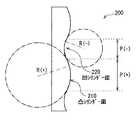
図35(A)に記載のパワー素子200は、凸シリンダー面210(第1光学面)と凹シリンダー面220(第2光学面)が交互に配列された凹凸面200Aをインテグレータ40側に有しており、さらに、平坦面200Bをインテグレータ40とは反対側に有している。凸シリンダー面210および凹シリンダー面220は、横方向と45度の角度で交差する方向に延在しており、さらに、これらの延在方向と直交する方向に交互に配列されている。凸シリンダー面210は、曲率半径R(+)の凸状曲面であり、平坦面200B側から入射した光を収束光束に変換するようになっている。凹シリンダー面220は、曲率半径R(−)の凹状曲面であり、平坦面200B側から入射した光を発散光束に変換するようになっている。凸シリンダー面210の曲率半径R(+)は、凹シリンダー面220の曲率半径R(−)よりも大きくなっている。さらに、凸シリンダー面210の幅P(+)(配列方向の幅)は、凹シリンダー面220の幅P(−)(配列方向の幅)よりも広くなっている。
The
ここで、図37中のF(+)は、凸シリンダー面210の焦点距離である。また、F(−)は、凹シリンダー面220の焦点距離である。θ(+)は、収束光束を構成する光線の進行方向と、インテグレータ40の光軸とのなす角度の最大値である。θ(−)は、発散光束を構成する光線の進行方向と、インテグレータ40の光軸とのなす角度の最大値である。LPは、凸シリンダー面210収束光束幅と、凹シリンダー面220の発散光束幅が互いに等しくなる箇所を含む面と、パワー素子200との距離である。Pは、凸シリンダー面210収束光束幅と、凹シリンダー面220の発散光束幅が互いに等しくなる箇所における両光束の幅である。Lは、パワー素子200とインテグレータ40との距離であり、具体的には、各凸シリンダー面210の頂部を含む面と、フライアイレンズ40Aの各セル41の頂部を含む面との距離である。なお、パワー素子200の各パラメータの値の一例を以下の表1に示す。

(変形例5)
また、上記実施の形態およびその変形例では、微小振動素子100は、光学素子110と、光学素子110を微小振動させる駆動部120とを有していたが、それらの代わりに、回折効果を利用した回折分岐素子と、回折分岐素子を微小振動させる駆動部とを有していてもよい。回折分岐素子は、入射光を回折させることにより複数の回折次数の光束に分岐して、各々異なる角度で射出させるものである。ただし、回折分岐素子は、当該回折分岐素子から出射された光のフライアイレンズ40Aへの入射角が、フライアイレンズ40Aの許容角以内となるように構成されていることが好ましい。また、駆動部は、回折分岐素子から出射された光のフライアイレンズ40Aへの入射角がフライアイレンズ40Aの許容角以内となるように、回折分岐素子を振動させることが好ましい。
(Modification 5)
In the above-described embodiment and its modification, the
(変形例6)
また、上記実施の形態およびその変形例では、微小振動素子100は、光学素子110と、光学素子110を微小振動させる駆動部120とを有していたが、それらの代わりに、拡散板と、拡散板を微小振動させる駆動部とを有していてもよい。ただし、拡散板は、当該拡散板から出射された光のフライアイレンズ40Aへの入射角が、フライアイレンズ40Aの許容角以内となるように構成されていることが好ましい。また、駆動部は、拡散板から出射された光のフライアイレンズ40Aへの入射角がフライアイレンズ40Aの許容角以内となるように、拡散板を振動させることが好ましい。
(Modification 6)
In the above-described embodiment and its modification, the
また、例えば、本技術は以下のような構成を取ることができる。
(1)
単一もしくは複数の発光スポットからなる光射出領域から光を発する第1の固体発光素子を含む第1の光源と、
前記第1の光源側から入射した光の指向角を変換する第1の指向角変換素子と、
前記第1の指向角変換素子を透過した光が照明する所定の照明範囲における光の照度分布を均一化するインテグレータと、
前記第1の光源と前記第1の指向角変換素子との間、または前記第1の指向角変換素子と前記インテグレータとの間に配置され、かつ前記照明範囲における照明状態を時間的に変化させる第1の微小振動素子と
を備え、
前記第1の固体発光素子は、レーザダイオードを含み、
前記インテグレータは、前記第1の指向角変換素子側からの光が入射する第1のフライアイレンズと、前記第1のフライアイレンズ側からの光が入射する第2のフライアイレンズとからなり、
前記第1のフライアイレンズの各セルによって前記第2のフライアイレンズに形成される各光源像のサイズが前記第2のフライアイレンズの1セルのサイズを超えない大きさとなるように、前記第1の指向角変換素子と、前記第1および第2のフライアイレンズとからなる光学系の光学倍率、および第1の微小振動素子の形状が設定され、
各光源像が、前記第2のフライアイレンズの複数のセルにまたがって形成されることがないように、第1の微小振動素子の振動振幅により前記光源像が変位する量が設定されている
照明装置。
(2)
前記第1の固体発光素子は、所定の波長帯の光を発する単一のチップ、または同一の波長帯もしくは互いに異なる波長帯の光を発する複数のチップからなり、
前記第1の微小振動素子の振動振幅により前記光源像が変位する量が以下の関係式を満たす
(1)に記載の照明装置。
h+d≦hFEL2
h:前記光源像のサイズ
d:前記第1の微小振動素子の振動により光源像が変位する量
hFEL2:前記第2のフライアイレンズの1セルのサイズ
(3)
前記第1および第2のフライアイレンズの各セルが1以外の縦横比を有しており、
前記第1の微小振動素子の振動振幅により前記光源像が変位する量が以下の関係式を満たす
(2)に記載の照明装置。
hx+dx≦hFEL2x
hy+dy≦hFEL2y
hx:前記光源像の第1の方向(前記第1および第2のフライアイレンズの各セルの長手方向またはそれに対応する方向)のサイズ
hy:前記光源像の、第1の方向と直交する第2の方向(前記第1および第2のフライアイレンズの各セルの短手方向またはそれに対応する方向)のサイズ
hFEL2x:前記第2のフライアイレンズの1セルの第1の方向のサイズ
hFEL2y:前記第2のフライアイレンズの1セルの第2の方向のサイズ
dx:前記第1の微小振動素子の振動振幅により光源像が変位する量のうち、第1の方向の成分(dx≧0、ただしdy=0のときはdx>0)
dy:前記第1の微小振動素子の振動振幅により光源像が変位する量のうち、第2の方向の成分(dy≧0、ただしdx=0のときはdy>0)
(4)
単一もしくは複数の発光スポットからなる光射出領域から光を発する第2の固体発光素子を含む第2の光源と、
前記第2の光源側から入射した光の指向角を変換する第2の指向角変換素子と、
前記第1および第2の指向角変換素子を透過した光を合成し、その合成光を前記インテグレータに向けて出力する光路合成素子と
をさらに備え、
前記第2の固体発光素子は、レーザダイオードを含み、
前記第1の微小振動素子は、前記光路合成素子と前記インテグレータとの間に配置されている
(1)ないし(3)のいずれか1つに記載の照明装置。
(5)
前記第1の微小振動素子が、前記第1の光源と前記第1の指向角変換素子との間、または前記第1の指向角変換素子と前記光路合成素子との間に配置され、
当該照明装置は、前記第2の光源と前記第2の指向角変換素子との間、または前記第2の指向角変換素子と前記光路合成素子との間に配置され、かつ前記照明範囲における照明状態を時間的に変化させる第2の微小振動素子をさらに備え、
各光源像が、前記第2のフライアイレンズの複数のセルにまたがって形成されることがないように、前記第2の微小振動素子の形状と、前記第2の微小振動素子の振動振幅により前記光源像が変位する量が設定されている
(4)に記載の照明装置。
(6)
前記第1の指向角変換素子の焦点距離が1以外の縦横比を有し、
前記第1および第2のフライアイレンズの各セルが1以外の縦横比を有し、
前記第1の指向角変換素子の縦横の焦点距離の比と、前記第2のフライアイレンズの各セルの縦横比の逆数とが、互いに等しくなっている
(1)ないし(5)のいずれか1つに記載の照明装置。
(7)
前記第1のフライアイレンズは、前記第2のフライアイレンズの略焦点位置に配置されており、
前記第2のフライアイレンズは、前記第1のフライアイレンズの略焦点位置に配置されている
(1)ないし(6)のいずれか1つに記載の照明装置。
(8)
前記第1の指向角変換素子と前記インテグレータとの間に設けられた偏光分離素子と、
前記インテグレータと前記照明範囲との間に設けられた位相差板アレイと
を備え、
前記第1の微小振動素子は、前記第1の光源と前記第1の指向角変換素子との間、または前記第1の指向角変換素子と前記偏光分離素子との間に配置されており、
前記偏光分離素子は、前記第1の指向角変換素子側から入射する光を、S偏光成分とP偏光成分との進行方向が異なるように分離し、
前記位相差板アレイは、位相差の互いに異なる第1領域および第2領域を有し、
前記第1領域は、前記偏光分離素子で分離されたS偏光成分およびP偏光成分のいずれか一方の偏光成分が入射する位置に配置されており、当該第1領域への入射光を、偏光方向を維持したまま透過し、
前記第2領域は、前記偏光分離素子で分離されたS偏光成分およびP偏光成分のうち前記第1領域に入射する偏光成分とは異なる偏光成分が入射する位置に配置されており、当該第2領域への入射光を、前記第1領域に入射する光の偏光と等しい偏光の光に変換する
(1)ないし(7)のいずれか1つに記載の照明装置。
(9)
前記第1領域および前記第2領域はともに、前記偏光分離素子における分離方向と直交する方向に延在する帯状の形状となっており、かつ前記偏光分離素子における分離方向と平行な方向に交互に配置されている
(8)に記載の照明装置。
(10)
前記第1および第2のフライアイレンズの各セルが1以外の縦横比を有し、
前記第1領域および前記第2領域はともに、前記第1および第2のフライアイレンズの長手方向と垂直な方向に延在する帯状の形状となっている
(8)に記載の照明装置。
(11)
前記位相差板アレイは、前記第1のフライアイレンズの略焦点位置に配置されており、
前記第2のフライアイレンズは、前記第1のフライアイレンズの焦点位置よりも手前に配置されている
(8)に記載の照明装置。
(12)
照明光学系と、
入力された映像信号に基づいて前記照明光学系からの光を変調することにより、画像光を生成する空間変調素子と、
前記空間変調素子で生成された画像光を投射する投影光学系と、
を備え、
前記照明光学系は、
レーザダイオードを含む第1の光源と、
前記第1の光源側から入射した光の指向角を変換する第1の指向角変換素子と、
前記第1の指向角変換素子を透過した光が照明する所定の照明範囲における光の照度分布を均一化するインテグレータと、
前記第1の光源と前記第1の指向角変換素子との間、または前記第1の指向角変換素子と前記インテグレータとの間に配置され、かつ前記照明範囲における照明状態を時間的に変化させる第1の微小振動素子と
を備え、
前記インテグレータは、前記第1の指向角変換素子側からの光が入射する第1のフライアイレンズと、前記第1のフライアイレンズ側からの光が入射する第2のフライアイレンズとからなり、
前記第1のフライアイレンズの各セルによって前記第2のフライアイレンズに形成される各光源像のサイズが前記第2のフライアイレンズの1セルのサイズを超えない大きさとなるように、前記第1の指向角変換素子と、前記第1および第2のフライアイレンズとからなる光学系の光学倍率と、前記第1の微小振動素子の形状と、前記第1の微小振動素子の振動振幅により前記光源像が変位する量とが設定されている
投射型表示装置。
(13)
照明光学系と、
入力された映像信号に基づいて前記照明光学系からの光を変調することにより、画像光を生成する空間変調素子と、
前記空間変調素子で生成された画像光を投射する投影光学系と、
前記投影光学系から投射された画像光を映し出す透過型スクリーンと
を備え、
前記照明光学系は、
レーザダイオードを含む第1の光源と、
前記第1の光源側から入射した光の指向角を変換する第1の指向角変換素子と、
前記第1の指向角変換素子を透過した光が照明する所定の照明範囲における光の照度分布を均一化するインテグレータと、
前記第1の光源と前記第1の指向角変換素子との間、または前記第1の指向角変換素子と前記インテグレータとの間に配置され、かつ前記照明範囲における照明状態を時間的に変化させる第1の微小振動素子と
を備え、
前記インテグレータは、前記第1の指向角変換素子側からの光が入射する第1のフライアイレンズと、前記第1のフライアイレンズ側からの光が入射する第2のフライアイレンズとからなり、
前記第1のフライアイレンズの各セルによって前記第2のフライアイレンズに形成される各光源像のサイズが前記第2のフライアイレンズの1セルのサイズを超えない大きさとなるように、前記第1の指向角変換素子と、前記第1および第2のフライアイレンズとからなる光学系の光学倍率と、前記第1の微小振動素子の振動振幅により前記光源像が変位する量とが設定されている
直視型表示装置。
For example, this technique can take the following composition.
(1)
A first light source including a first solid-state light-emitting element that emits light from a light emission region composed of a single or a plurality of light-emitting spots;
A first directivity angle conversion element that converts the directivity angle of light incident from the first light source side;
An integrator for equalizing an illuminance distribution of light in a predetermined illumination range illuminated by light transmitted through the first directivity angle conversion element;
It is arranged between the first light source and the first directivity angle conversion element or between the first directivity angle conversion element and the integrator, and changes the illumination state in the illumination range with time. A first micro vibration element,
The first solid state light emitting device includes a laser diode,
The integrator includes a first fly-eye lens into which light from the first directivity angle conversion element side enters and a second fly-eye lens into which light from the first fly-eye lens side enters. ,
The size of each light source image formed on the second fly-eye lens by each cell of the first fly-eye lens is not larger than the size of one cell of the second fly-eye lens. The optical magnification of the optical system composed of the first directivity angle conversion element and the first and second fly-eye lenses, and the shape of the first micro-vibration element are set,
The amount by which the light source image is displaced by the vibration amplitude of the first micro vibrating element is set so that each light source image is not formed across a plurality of cells of the second fly-eye lens. Lighting device.
(2)
The first solid state light emitting device comprises a single chip that emits light of a predetermined wavelength band, or a plurality of chips that emit light of the same wavelength band or different wavelength bands,
The lighting device according to (1), wherein an amount of displacement of the light source image by a vibration amplitude of the first micro vibrating element satisfies the following relational expression.
h + d ≦ h FEL2
h: Size of the light source image d: Amount of displacement of the light source image due to vibration of the first micro vibrating element h FEL2 : Size of one cell of the second fly-eye lens (3)
Each cell of the first and second fly's eye lenses has an aspect ratio other than 1,
The lighting device according to (2), wherein an amount of displacement of the light source image by a vibration amplitude of the first micro vibrating element satisfies the following relational expression.
h x + d x ≦ h FEL2x
h y + d y ≦ h FEL2y
h x : size of the first direction of the light source image (longitudinal direction of each cell of the first and second fly-eye lenses or a direction corresponding thereto) h y : orthogonal to the first direction of the light source image Size of the second direction (the short direction of each cell of the first and second fly-eye lenses or the direction corresponding thereto) h FEL2x : the first direction of one cell of the second fly-eye lens Size h FEL2y : Size in the second direction of one cell of the second fly-eye lens d x : Component in the first direction out of the amount of displacement of the light source image due to the vibration amplitude of the first micro vibrating element (D x ≧ 0, but d x > 0 when d y = 0)
d y : component in the second direction of the amount of displacement of the light source image due to the vibration amplitude of the first micro-vibration element (d y ≧ 0, but d y > 0 when d x = 0)
(4)
A second light source including a second solid-state light emitting element that emits light from a light emission region composed of a single or a plurality of light emitting spots;
A second directivity angle conversion element for converting the directivity angle of light incident from the second light source side;
An optical path combining element that combines light transmitted through the first and second directivity angle conversion elements and outputs the combined light to the integrator;
The second solid state light emitting device includes a laser diode,
The lighting device according to any one of (1) to (3), wherein the first micro vibrating element is disposed between the optical path combining element and the integrator.
(5)
The first micro-vibration element is disposed between the first light source and the first directivity angle conversion element or between the first directivity angle conversion element and the optical path synthesis element;
The illumination device is disposed between the second light source and the second directivity angle conversion element, or between the second directivity angle conversion element and the optical path synthesis element, and illumination in the illumination range A second micro-vibration element that changes the state over time;
The shape of the second micro-vibration element and the vibration amplitude of the second micro-vibration element are set so that each light source image is not formed across a plurality of cells of the second fly-eye lens. The amount by which the light source image is displaced is set.
(6)
The focal length of the first directivity conversion element has an aspect ratio other than 1;
Each cell of the first and second fly's eye lenses has an aspect ratio other than 1,
The ratio of the vertical and horizontal focal lengths of the first directivity conversion element and the reciprocal of the aspect ratio of each cell of the second fly's eye lens are equal to each other (1) to (5) The lighting device according to one.
(7)
The first fly-eye lens is disposed at a substantially focal position of the second fly-eye lens,
The lighting device according to any one of (1) to (6), wherein the second fly-eye lens is disposed at a substantially focal position of the first fly-eye lens.
(8)
A polarization separation element provided between the first directivity angle conversion element and the integrator;
A phase difference plate array provided between the integrator and the illumination range,
The first micro-vibration element is disposed between the first light source and the first directivity angle conversion element, or between the first directivity angle conversion element and the polarization separation element,
The polarization separation element separates the light incident from the first directivity angle conversion element side so that the traveling directions of the S-polarized component and the P-polarized component are different,
The phase difference plate array has a first region and a second region having different phase differences,
The first region is arranged at a position where one of the S-polarized component and the P-polarized component separated by the polarization separation element is incident, and the incident light to the first region is changed in the polarization direction. While maintaining
The second region is disposed at a position where a polarization component different from a polarization component incident on the first region is incident among the S polarization component and the P polarization component separated by the polarization separation element. The illumination device according to any one of (1) to (7), wherein light incident on the region is converted into light having a polarization equal to that of light incident on the first region.
(9)
Both the first region and the second region have a band shape extending in a direction orthogonal to the separation direction in the polarization separation element, and alternately in a direction parallel to the separation direction in the polarization separation element. It is arrange | positioned. The illuminating device as described in (8).
(10)
Each cell of the first and second fly's eye lenses has an aspect ratio other than 1,
Both said 1st area | region and said 2nd area | region are the strip | belt-shaped shape extended in the direction perpendicular | vertical to the longitudinal direction of said 1st and 2nd fly eye lens.
(11)
The phase difference plate array is disposed at a substantially focal position of the first fly-eye lens,
The lighting apparatus according to (8), wherein the second fly-eye lens is disposed in front of a focal position of the first fly-eye lens.
(12)
Illumination optics,
A spatial modulation element that generates image light by modulating light from the illumination optical system based on an input video signal;
A projection optical system that projects image light generated by the spatial modulation element;
With
The illumination optical system includes:
A first light source including a laser diode;
A first directivity angle conversion element that converts the directivity angle of light incident from the first light source side;
An integrator for equalizing an illuminance distribution of light in a predetermined illumination range illuminated by light transmitted through the first directivity angle conversion element;
It is arranged between the first light source and the first directivity angle conversion element or between the first directivity angle conversion element and the integrator, and changes the illumination state in the illumination range with time. A first micro vibration element,
The integrator includes a first fly-eye lens into which light from the first directivity angle conversion element side enters and a second fly-eye lens into which light from the first fly-eye lens side enters. ,
The size of each light source image formed on the second fly-eye lens by each cell of the first fly-eye lens is not larger than the size of one cell of the second fly-eye lens. The optical magnification of the optical system composed of the first directivity angle conversion element and the first and second fly-eye lenses, the shape of the first micro-vibration element, and the vibration amplitude of the first micro-vibration element The amount by which the light source image is displaced is set by the projection type display device.
(13)
Illumination optics,
A spatial modulation element that generates image light by modulating light from the illumination optical system based on an input video signal;
A projection optical system that projects image light generated by the spatial modulation element;
A transmissive screen that projects the image light projected from the projection optical system,
The illumination optical system includes:
A first light source including a laser diode;
A first directivity angle conversion element that converts the directivity angle of light incident from the first light source side;
An integrator for equalizing an illuminance distribution of light in a predetermined illumination range illuminated by light transmitted through the first directivity angle conversion element;
It is arranged between the first light source and the first directivity angle conversion element or between the first directivity angle conversion element and the integrator, and changes the illumination state in the illumination range with time. A first micro vibration element,
The integrator includes a first fly-eye lens into which light from the first directivity angle conversion element side enters and a second fly-eye lens into which light from the first fly-eye lens side enters. ,
The size of each light source image formed on the second fly-eye lens by each cell of the first fly-eye lens is not larger than the size of one cell of the second fly-eye lens. The optical magnification of the optical system composed of the first directivity angle conversion element, the first and second fly-eye lenses, and the amount by which the light source image is displaced by the vibration amplitude of the first minute vibration element are set. Direct view type display device.
1,3,4,5…プロジェクタ、1A,3A,4A,5A…照明光学系、2…スクリーン、6…リアプロジェクション表示装置、7…透過型スクリーン、10A,10B,10C、10D…光源、11…固体発光素子、11A…チップ、11B…発光スポット、12…パッケージ、13…ステム、13A…支持基板、13B…外枠基板、13C…接続端子、14…キャップ、14A…筒部、14B…光透過部、15…サブマウント、16…ワイヤ、20A,20B,20C,20D…カップリングレンズ、30…光路合成素子、30A,30B,30C…ダイクロイックミラー、40…インテグレータ、40A,40B…フライアイレンズ、41,42…セル、50…コンデンサレンズ、60…空間変調素子、60A…照明範囲、70…投影光学系、80…偏光分離素子、90…位相差板アレイ、90A…第1領域、90B…第2領域、100…微小振動素子、200…パワー素子。
DESCRIPTION OF
Claims (13)
前記第1の光源側から入射した光の指向角を変換する第1の指向角変換素子と、
前記第1の指向角変換素子を透過した光が照明する所定の照明範囲における光の照度分布を均一化するインテグレータと、
前記第1の光源と前記第1の指向角変換素子との間、または前記第1の指向角変換素子と前記インテグレータとの間に配置され、かつ前記照明範囲における照明状態を時間的に変化させる第1の微小振動素子と
を備え、
前記第1の固体発光素子は、レーザダイオードを含み、
前記インテグレータは、前記第1の指向角変換素子側からの光が入射する第1のフライアイレンズと、前記第1のフライアイレンズ側からの光が入射する第2のフライアイレンズとからなり、
前記第1のフライアイレンズの各セルによって前記第2のフライアイレンズに形成される各光源像のサイズが前記第2のフライアイレンズの1セルのサイズを超えない大きさとなるように、前記第1の指向角変換素子と、前記第1および第2のフライアイレンズとからなる光学系の光学倍率、および第1の微小振動素子の形状が設定され、
各光源像が、前記第2のフライアイレンズの複数のセルにまたがって形成されることがないように、第1の微小振動素子の振動振幅により前記光源像が変位する量が設定されている
照明装置。 A first light source including a first solid-state light-emitting element that emits light from a light emission region composed of a single or a plurality of light-emitting spots;
A first directivity angle conversion element that converts the directivity angle of light incident from the first light source side;
An integrator for equalizing an illuminance distribution of light in a predetermined illumination range illuminated by light transmitted through the first directivity angle conversion element;
It is arranged between the first light source and the first directivity angle conversion element or between the first directivity angle conversion element and the integrator, and changes the illumination state in the illumination range with time. A first micro vibration element,
The first solid state light emitting device includes a laser diode,
The integrator includes a first fly-eye lens into which light from the first directivity angle conversion element side enters and a second fly-eye lens into which light from the first fly-eye lens side enters. ,
The size of each light source image formed on the second fly-eye lens by each cell of the first fly-eye lens is not larger than the size of one cell of the second fly-eye lens. The optical magnification of the optical system composed of the first directivity angle conversion element and the first and second fly-eye lenses, and the shape of the first micro-vibration element are set,
The amount by which the light source image is displaced by the vibration amplitude of the first micro vibrating element is set so that each light source image is not formed across a plurality of cells of the second fly-eye lens. Lighting device.
前記第1の微小振動素子の振動振幅により前記光源像が変位する量が以下の関係式を満たす
請求項1に記載の照明装置。
h+d≦hFEL2
h:前記光源像のサイズ
d:前記第1の微小振動素子の振動により光源像が変位する量
hFEL2:前記第2のフライアイレンズの1セルのサイズ The first solid state light emitting device comprises a single chip that emits light of a predetermined wavelength band, or a plurality of chips that emit light of the same wavelength band or different wavelength bands,
The lighting device according to claim 1, wherein an amount of displacement of the light source image by a vibration amplitude of the first micro vibrating element satisfies the following relational expression.
h + d ≦ h FEL2
h: Size of the light source image d: Amount of displacement of the light source image due to vibration of the first micro vibrating element h FEL2 : Size of one cell of the second fly-eye lens
前記第1の微小振動素子の振動振幅により前記光源像が変位する量が以下の関係式を満たす
請求項2に記載の照明装置。
hx+dx≦hFEL2x
hy+dy≦hFEL2y
hx:前記光源像の第1の方向(前記第1および第2のフライアイレンズの各セルの長手方向またはそれに対応する方向)のサイズ
hy:前記光源像の、第1の方向と直交する第2の方向(前記第1および第2のフライアイレンズの各セルの短手方向またはそれに対応する方向)のサイズ
hFEL2x:前記第2のフライアイレンズの1セルの第1の方向のサイズ
hFEL2y:前記第2のフライアイレンズの1セルの第2の方向のサイズ
dx:前記第1の微小振動素子の振動振幅により光源像が変位する量のうち、第1の方向の成分(dx≧0、ただしdy=0のときはdx>0)
dy:前記第1の微小振動素子の振動振幅により光源像が変位する量のうち、第2の方向の成分(dy≧0、ただしdx=0のときはdy>0) Each cell of the first and second fly's eye lenses has an aspect ratio other than 1,
The lighting device according to claim 2, wherein an amount of displacement of the light source image by a vibration amplitude of the first micro vibrating element satisfies the following relational expression.
h x + d x ≦ h FEL2x
h y + d y ≦ h FEL2y
h x : size of the first direction of the light source image (longitudinal direction of each cell of the first and second fly-eye lenses or a direction corresponding thereto) h y : orthogonal to the first direction of the light source image Size of the second direction (the short direction of each cell of the first and second fly-eye lenses or the direction corresponding thereto) h FEL2x : the first direction of one cell of the second fly-eye lens Size h FEL2y : Size in the second direction of one cell of the second fly-eye lens d x : Component in the first direction out of the amount of displacement of the light source image due to the vibration amplitude of the first micro vibrating element (D x ≧ 0, but d x > 0 when d y = 0)
d y : component in the second direction of the amount of displacement of the light source image due to the vibration amplitude of the first micro-vibration element (d y ≧ 0, but d y > 0 when d x = 0)
前記第2の光源側から入射した光の指向角を変換する第2の指向角変換素子と、
前記第1および第2の指向角変換素子を透過した光を合成し、その合成光を前記インテグレータに向けて出力する光路合成素子と
をさらに備え、
前記第2の固体発光素子は、レーザダイオードを含み、
前記第1の微小振動素子は、前記光路合成素子と前記インテグレータとの間に配置されている
請求項1ないし請求項3のいずれか一項に記載の照明装置。 A second light source including a second solid-state light emitting element that emits light from a light emission region composed of a single or a plurality of light emitting spots;
A second directivity angle conversion element for converting the directivity angle of light incident from the second light source side;
An optical path combining element that combines light transmitted through the first and second directivity angle conversion elements and outputs the combined light to the integrator;
The second solid state light emitting device includes a laser diode,
The lighting device according to any one of claims 1 to 3, wherein the first micro vibrating element is disposed between the optical path combining element and the integrator.
当該照明装置は、前記第2の光源と前記第2の指向角変換素子との間、または前記第2の指向角変換素子と前記光路合成素子との間に配置され、かつ前記照明範囲における照明状態を時間的に変化させる第2の微小振動素子をさらに備え、
各光源像が、前記第2のフライアイレンズの複数のセルにまたがって形成されることがないように、前記第2の微小振動素子の形状と、前記第2の微小振動素子の振動振幅により前記光源像が変位する量が設定されている
請求項4に記載の照明装置。 The first micro-vibration element is disposed between the first light source and the first directivity angle conversion element or between the first directivity angle conversion element and the optical path synthesis element;
The illumination device is disposed between the second light source and the second directivity angle conversion element, or between the second directivity angle conversion element and the optical path synthesis element, and illumination in the illumination range A second micro-vibration element that changes the state over time;
The shape of the second micro-vibration element and the vibration amplitude of the second micro-vibration element are set so that each light source image is not formed across a plurality of cells of the second fly-eye lens. The illumination device according to claim 4, wherein an amount of displacement of the light source image is set.
前記第1および第2のフライアイレンズの各セルが1以外の縦横比を有し、
前記第1の指向角変換素子の縦横の焦点距離の比と、前記第2のフライアイレンズの各セルの縦横比の逆数とが、互いに等しくなっている
請求項1ないし請求項5のいずれか一項に記載の照明装置。 The focal length of the first directivity conversion element has an aspect ratio other than 1;
Each cell of the first and second fly's eye lenses has an aspect ratio other than 1,
The ratio of the longitudinal and lateral focal lengths of the first directivity angle conversion element and the reciprocal of the aspect ratio of each cell of the second fly's eye lens are equal to each other . The lighting device according to one item .
前記第2のフライアイレンズは、前記第1のフライアイレンズの略焦点位置に配置されている
請求項1ないし請求項6のいずれか一項に記載の照明装置。 The first fly-eye lens is disposed at a substantially focal position of the second fly-eye lens,
The lighting device according to any one of claims 1 to 6, wherein the second fly-eye lens is disposed at a substantially focal position of the first fly-eye lens.
前記インテグレータと前記照明範囲との間に設けられた位相差板アレイと
を備え、
前記第1の微小振動素子は、前記第1の光源と前記第1の指向角変換素子との間、または前記第1の指向角変換素子と前記偏光分離素子との間に配置されており、
前記偏光分離素子は、前記第1の指向角変換素子側から入射する光を、S偏光成分とP偏光成分との進行方向が異なるように分離し、
前記位相差板アレイは、位相差の互いに異なる第1領域および第2領域を有し、
前記第1領域は、前記偏光分離素子で分離されたS偏光成分およびP偏光成分のいずれか一方の偏光成分が入射する位置に配置されており、当該第1領域への入射光を、偏光方向を維持したまま透過し、
前記第2領域は、前記偏光分離素子で分離されたS偏光成分およびP偏光成分のうち前記第1領域に入射する偏光成分とは異なる偏光成分が入射する位置に配置されており、当該第2領域への入射光を、前記第1領域に入射する光の偏光と等しい偏光の光に変換する
請求項1ないし請求項7のいずれか一項に記載の照明装置。 A polarization separation element provided between the first directivity angle conversion element and the integrator;
A phase difference plate array provided between the integrator and the illumination range,
The first micro-vibration element is disposed between the first light source and the first directivity angle conversion element, or between the first directivity angle conversion element and the polarization separation element,
The polarization separation element separates the light incident from the first directivity angle conversion element side so that the traveling directions of the S-polarized component and the P-polarized component are different,
The phase difference plate array has a first region and a second region having different phase differences,
The first region is arranged at a position where one of the S-polarized component and the P-polarized component separated by the polarization separation element is incident, and the incident light to the first region is changed in the polarization direction. While maintaining
The second region is disposed at a position where a polarization component different from a polarization component incident on the first region is incident among the S polarization component and the P polarization component separated by the polarization separation element. The illumination device according to any one of claims 1 to 7 , wherein incident light to the region is converted into light having a polarization equal to that of light incident on the first region.
請求項8に記載の照明装置。 Both the first region and the second region have a band shape extending in a direction orthogonal to the separation direction in the polarization separation element, and alternately in a direction parallel to the separation direction in the polarization separation element. The lighting device according to claim 8, wherein the lighting device is arranged.
前記第1領域および前記第2領域はともに、前記第1および第2のフライアイレンズの長手方向と垂直な方向に延在する帯状の形状となっている
請求項8に記載の照明装置。 Each cell of the first and second fly's eye lenses has an aspect ratio other than 1,
The lighting device according to claim 8, wherein both the first region and the second region have a belt-like shape extending in a direction perpendicular to a longitudinal direction of the first and second fly-eye lenses.
前記第2のフライアイレンズは、前記第1のフライアイレンズの焦点位置よりも手前に配置されている
請求項8に記載の照明装置。 The phase difference plate array is disposed at a substantially focal position of the first fly-eye lens,
The lighting device according to claim 8, wherein the second fly-eye lens is disposed in front of a focal position of the first fly-eye lens.
入力された映像信号に基づいて前記照明光学系からの光を変調することにより、画像光を生成する空間変調素子と、
前記空間変調素子で生成された画像光を投射する投影光学系と、
を備え、
前記照明光学系は、
レーザダイオードを含む第1の光源と、
前記第1の光源側から入射した光の指向角を変換する第1の指向角変換素子と、
前記第1の指向角変換素子を透過した光が照明する所定の照明範囲における光の照度分布を均一化するインテグレータと、
前記第1の光源と前記第1の指向角変換素子との間、または前記第1の指向角変換素子と前記インテグレータとの間に配置され、かつ前記照明範囲における照明状態を時間的に変化させる第1の微小振動素子と
を備え、
前記インテグレータは、前記第1の指向角変換素子側からの光が入射する第1のフライアイレンズと、前記第1のフライアイレンズ側からの光が入射する第2のフライアイレンズとからなり、
前記第1のフライアイレンズの各セルによって前記第2のフライアイレンズに形成される各光源像のサイズが前記第2のフライアイレンズの1セルのサイズを超えない大きさとなるように、前記第1の指向角変換素子と、前記第1および第2のフライアイレンズとからなる光学系の光学倍率と、前記第1の微小振動素子の形状と、前記第1の微小振動素子の振動振幅により前記光源像が変位する量とが設定されている
投射型表示装置。 Illumination optics,
A spatial modulation element that generates image light by modulating light from the illumination optical system based on an input video signal;
A projection optical system that projects image light generated by the spatial modulation element;
With
The illumination optical system includes:
A first light source including a laser diode;
A first directivity angle conversion element that converts the directivity angle of light incident from the first light source side;
An integrator for equalizing an illuminance distribution of light in a predetermined illumination range illuminated by light transmitted through the first directivity angle conversion element;
It is arranged between the first light source and the first directivity angle conversion element or between the first directivity angle conversion element and the integrator, and changes the illumination state in the illumination range with time. A first micro vibration element,
The integrator includes a first fly-eye lens into which light from the first directivity angle conversion element side enters and a second fly-eye lens into which light from the first fly-eye lens side enters. ,
The size of each light source image formed on the second fly-eye lens by each cell of the first fly-eye lens is not larger than the size of one cell of the second fly-eye lens. The optical magnification of the optical system composed of the first directivity angle conversion element and the first and second fly-eye lenses, the shape of the first micro-vibration element, and the vibration amplitude of the first micro-vibration element The amount by which the light source image is displaced is set by the projection type display device.
入力された映像信号に基づいて前記照明光学系からの光を変調することにより、画像光を生成する空間変調素子と、
前記空間変調素子で生成された画像光を投射する投影光学系と、
前記投影光学系から投射された画像光を映し出す透過型スクリーンと
を備え、
前記照明光学系は、
レーザダイオードを含む第1の光源と、
前記第1の光源側から入射した光の指向角を変換する第1の指向角変換素子と、
前記第1の指向角変換素子を透過した光が照明する所定の照明範囲における光の照度分布を均一化するインテグレータと、
前記第1の光源と前記第1の指向角変換素子との間、または前記第1の指向角変換素子と前記インテグレータとの間に配置され、かつ前記照明範囲における照明状態を時間的に変化させる第1の微小振動素子と
を備え、
前記インテグレータは、前記第1の指向角変換素子側からの光が入射する第1のフライアイレンズと、前記第1のフライアイレンズ側からの光が入射する第2のフライアイレンズとからなり、
前記第1のフライアイレンズの各セルによって前記第2のフライアイレンズに形成される各光源像のサイズが前記第2のフライアイレンズの1セルのサイズを超えない大きさとなるように、前記第1の指向角変換素子と、前記第1および第2のフライアイレンズとからなる光学系の光学倍率と、前記第1の微小振動素子の形状と、前記第1の微小振動素子の振動振幅により前記光源像が変位する量とが設定されている
直視型表示装置。 Illumination optics,
A spatial modulation element that generates image light by modulating light from the illumination optical system based on an input video signal;
A projection optical system that projects image light generated by the spatial modulation element;
A transmissive screen that projects the image light projected from the projection optical system,
The illumination optical system includes:
A first light source including a laser diode;
A first directivity angle conversion element that converts the directivity angle of light incident from the first light source side;
An integrator for equalizing an illuminance distribution of light in a predetermined illumination range illuminated by light transmitted through the first directivity angle conversion element;
It is arranged between the first light source and the first directivity angle conversion element or between the first directivity angle conversion element and the integrator, and changes the illumination state in the illumination range with time. A first micro vibration element,
The integrator includes a first fly-eye lens into which light from the first directivity angle conversion element side enters and a second fly-eye lens into which light from the first fly-eye lens side enters. ,
The size of each light source image formed on the second fly-eye lens by each cell of the first fly-eye lens is not larger than the size of one cell of the second fly-eye lens. The optical magnification of the optical system composed of the first directivity angle conversion element and the first and second fly-eye lenses, the shape of the first micro-vibration element, and the vibration amplitude of the first micro-vibration element The amount by which the light source image is displaced is set by the direct view type display device.
Priority Applications (3)
| Application Number | Priority Date | Filing Date | Title |
|---|---|---|---|
| JP2011258665A JP5811807B2 (en) | 2011-03-22 | 2011-11-28 | Illumination device, projection display device, direct view display device |
| CN201210059089.XA CN102692801B (en) | 2011-03-22 | 2012-03-07 | Illuminator, projection type display and direct viewing type display |
| US13/414,797 US8616706B2 (en) | 2011-03-22 | 2012-03-08 | Illumination device, projection display, and direct-view display |
Applications Claiming Priority (3)
| Application Number | Priority Date | Filing Date | Title |
|---|---|---|---|
| JP2011062923 | 2011-03-22 | ||
| JP2011062923 | 2011-03-22 | ||
| JP2011258665A JP5811807B2 (en) | 2011-03-22 | 2011-11-28 | Illumination device, projection display device, direct view display device |
Publications (3)
| Publication Number | Publication Date |
|---|---|
| JP2012212099A JP2012212099A (en) | 2012-11-01 |
| JP2012212099A5 JP2012212099A5 (en) | 2014-12-04 |
| JP5811807B2 true JP5811807B2 (en) | 2015-11-11 |
Family
ID=46858360
Family Applications (1)
| Application Number | Title | Priority Date | Filing Date |
|---|---|---|---|
| JP2011258665A Active JP5811807B2 (en) | 2011-03-22 | 2011-11-28 | Illumination device, projection display device, direct view display device |
Country Status (3)
| Country | Link |
|---|---|
| US (1) | US8616706B2 (en) |
| JP (1) | JP5811807B2 (en) |
| CN (1) | CN102692801B (en) |
Families Citing this family (13)
| Publication number | Priority date | Publication date | Assignee | Title |
|---|---|---|---|---|
| JP5773661B2 (en) * | 2011-01-20 | 2015-09-02 | 株式会社ニューフレアテクノロジー | Illumination device, pattern inspection device, and method of forming illumination light |
| CN104871043B (en) | 2012-12-28 | 2017-09-26 | 旭硝子株式会社 | The manufacture method of optical element, projection arrangement and optical element |
| JP6136258B2 (en) * | 2012-12-28 | 2017-05-31 | 旭硝子株式会社 | Projection device |
| JP2014153636A (en) * | 2013-02-13 | 2014-08-25 | Canon Inc | Illumination optical system and image projection apparatus |
| EP3042312B1 (en) * | 2013-09-03 | 2021-06-09 | Seeing Machines Limited | Low power eye tracking system and method |
| JP6252298B2 (en) * | 2014-03-27 | 2017-12-27 | 大日本印刷株式会社 | Lighting device |
| KR101858973B1 (en) * | 2015-04-30 | 2018-05-17 | 에스케이텔레콤 주식회사 | Speckle reducing apparatus |
| JP6880694B2 (en) * | 2016-12-13 | 2021-06-02 | セイコーエプソン株式会社 | Lighting equipment and projectors |
| CN110579928A (en) * | 2018-06-08 | 2019-12-17 | 中强光电股份有限公司 | Projection device and head-mounted display device |
| KR101919735B1 (en) | 2018-07-16 | 2018-11-16 | (주)카네비컴 | A optical system capable of adjusting a beam angle, a Lidar sensor and adjustable emitting angle method |
| CN111258159B (en) * | 2018-11-30 | 2022-07-12 | 中强光电股份有限公司 | Illumination system and projection device |
| CN112815272B (en) * | 2019-11-18 | 2023-10-10 | 深圳市绎立锐光科技开发有限公司 | Light source system and light emitting device |
| CN113253557B (en) * | 2021-04-30 | 2022-08-02 | 电子科技大学 | Projector system based on Fresnel lens |
Family Cites Families (22)
| Publication number | Priority date | Publication date | Assignee | Title |
|---|---|---|---|---|
| JPS5565940A (en) | 1978-11-13 | 1980-05-17 | Matsushita Electric Ind Co Ltd | Laser image display device |
| US5313479A (en) | 1992-07-29 | 1994-05-17 | Texas Instruments Incorporated | Speckle-free display system using coherent light |
| DE69532691T2 (en) * | 1994-12-28 | 2005-02-10 | Seiko Epson Corp. | Polarization illumination device and projector using the same |
| CN1244277A (en) * | 1997-09-22 | 2000-02-09 | 索尼公司 | Image display |
| JPH11260144A (en) * | 1998-03-12 | 1999-09-24 | Matsushita Electric Ind Co Ltd | Lens element, illumination optical system and projection-type display unit using the same |
| JP2001343706A (en) * | 2000-05-31 | 2001-12-14 | Sony Corp | Video display device |
| JP5463613B2 (en) | 2006-11-27 | 2014-04-09 | 株式会社リコー | Illumination optical system, display device, and projection display device |
| WO2008114502A1 (en) * | 2007-03-19 | 2008-09-25 | Panasonic Corporation | Laser illuminating device and image display device |
| TWM324785U (en) * | 2007-04-16 | 2008-01-01 | Young Optics Inc | Illumination system |
| US20100245773A1 (en) * | 2007-08-29 | 2010-09-30 | Shinichi Arita | Image display apparatus |
| CN101825832B (en) * | 2009-03-06 | 2012-08-22 | 上海三鑫科技发展有限公司 | Laser optical engine |
| EP2600473B1 (en) * | 2010-07-30 | 2019-01-09 | Sony Corporation | Light source unit, illumination device, and display device |
| JP5195991B2 (en) * | 2010-10-04 | 2013-05-15 | ソニー株式会社 | Illumination device and display device |
| JP5581958B2 (en) * | 2010-10-12 | 2014-09-03 | ソニー株式会社 | Illumination device, projection display device, direct view display device |
| JP2012088451A (en) * | 2010-10-18 | 2012-05-10 | Sony Corp | Lighting device and display device |
| JP2012113223A (en) * | 2010-11-26 | 2012-06-14 | Sony Corp | Illuminating device, projection type display device, and direct-view type display device |
| JP5633695B2 (en) * | 2010-11-29 | 2014-12-03 | ソニー株式会社 | Illumination device, projection display device, and direct view display device |
| JP5648556B2 (en) * | 2011-03-28 | 2015-01-07 | ソニー株式会社 | Illumination device, projection display device, and direct view display device |
| CN202008573U (en) * | 2011-03-31 | 2011-10-12 | 上海三鑫科技发展有限公司 | laser projection optics with double compound eye lens |
| JP2012226292A (en) * | 2011-04-04 | 2012-11-15 | Sony Corp | Luminaire and display device |
| JP5978612B2 (en) * | 2011-07-13 | 2016-08-24 | ソニー株式会社 | Illumination device and display device |
| JP2013092745A (en) * | 2011-10-07 | 2013-05-16 | Sony Corp | Projection display |
-
2011
- 2011-11-28 JP JP2011258665A patent/JP5811807B2/en active Active
-
2012
- 2012-03-07 CN CN201210059089.XA patent/CN102692801B/en not_active Expired - Fee Related
- 2012-03-08 US US13/414,797 patent/US8616706B2/en active Active
Also Published As
| Publication number | Publication date |
|---|---|
| CN102692801A (en) | 2012-09-26 |
| US20120242961A1 (en) | 2012-09-27 |
| CN102692801B (en) | 2016-08-03 |
| US8616706B2 (en) | 2013-12-31 |
| JP2012212099A (en) | 2012-11-01 |
Similar Documents
| Publication | Publication Date | Title |
|---|---|---|
| JP5811807B2 (en) | Illumination device, projection display device, direct view display device | |
| JP5581958B2 (en) | Illumination device, projection display device, direct view display device | |
| JP5648556B2 (en) | Illumination device, projection display device, and direct view display device | |
| JP5633695B2 (en) | Illumination device, projection display device, and direct view display device | |
| JP5772143B2 (en) | Illumination device, projection display device, and direct view display device | |
| US9609294B2 (en) | Illumination device, projection type image display device, and optical device | |
| US9651795B2 (en) | Image display device | |
| US20130050285A1 (en) | Illumination device and display device | |
| JP5195991B2 (en) | Illumination device and display device | |
| JP5910324B2 (en) | Illumination device, projection display device, and direct view display device | |
| JP2012203392A (en) | Lighting system, projection display and direct-view display | |
| EP2587806B1 (en) | Illumination unit, projection display unit, and direct view display unit | |
| US11015781B2 (en) | Light source apparatus, light source unit, and image display apparatus | |
| JPWO2008041559A1 (en) | Surface illumination device and liquid crystal display device using the same | |
| JP2012203392A5 (en) | ||
| JP7071101B2 (en) | Light source device and image projection device | |
| JPWO2008111275A1 (en) | Illumination device and image projection device | |
| JP2012073496A (en) | Illumination device, projection type display device and direct-view display device | |
| JP2015007774A (en) | Lighting device, projection type display device, and direct-view display device | |
| JP5500235B2 (en) | Illumination device and display device | |
| JP2016118732A (en) | Image display device, light source device, and image display method |
Legal Events
| Date | Code | Title | Description |
|---|---|---|---|
| A521 | Written amendment |
Free format text: JAPANESE INTERMEDIATE CODE: A523 Effective date: 20141020 |
|
| A621 | Written request for application examination |
Free format text: JAPANESE INTERMEDIATE CODE: A621 Effective date: 20141020 |
|
| A977 | Report on retrieval |
Free format text: JAPANESE INTERMEDIATE CODE: A971007 Effective date: 20150820 |
|
| TRDD | Decision of grant or rejection written | ||
| A01 | Written decision to grant a patent or to grant a registration (utility model) |
Free format text: JAPANESE INTERMEDIATE CODE: A01 Effective date: 20150825 |
|
| A61 | First payment of annual fees (during grant procedure) |
Free format text: JAPANESE INTERMEDIATE CODE: A61 Effective date: 20150907 |
|
| R151 | Written notification of patent or utility model registration |
Ref document number: 5811807 Country of ref document: JP Free format text: JAPANESE INTERMEDIATE CODE: R151 |
|
| R250 | Receipt of annual fees |
Free format text: JAPANESE INTERMEDIATE CODE: R250 |
|
| R250 | Receipt of annual fees |
Free format text: JAPANESE INTERMEDIATE CODE: R250 |
|
| R250 | Receipt of annual fees |
Free format text: JAPANESE INTERMEDIATE CODE: R250 |