EP2434579A1 - Antenna device - Google Patents
Antenna device Download PDFInfo
- Publication number
- EP2434579A1 EP2434579A1 EP10777771A EP10777771A EP2434579A1 EP 2434579 A1 EP2434579 A1 EP 2434579A1 EP 10777771 A EP10777771 A EP 10777771A EP 10777771 A EP10777771 A EP 10777771A EP 2434579 A1 EP2434579 A1 EP 2434579A1
- Authority
- EP
- European Patent Office
- Prior art keywords
- power supply
- supply cord
- antenna
- frequency
- antenna device
- Prior art date
- Legal status (The legal status is an assumption and is not a legal conclusion. Google has not performed a legal analysis and makes no representation as to the accuracy of the status listed.)
- Granted
Links
Images


Classifications
-
- H—ELECTRICITY
- H01—ELECTRIC ELEMENTS
- H01Q—ANTENNAS, i.e. RADIO AERIALS
- H01Q1/00—Details of, or arrangements associated with, antennas
- H01Q1/44—Details of, or arrangements associated with, antennas using equipment having another main function to serve additionally as an antenna, e.g. means for giving an antenna an aesthetic aspect
- H01Q1/46—Electric supply lines or communication lines
-
- H—ELECTRICITY
- H01—ELECTRIC ELEMENTS
- H01Q—ANTENNAS, i.e. RADIO AERIALS
- H01Q1/00—Details of, or arrangements associated with, antennas
- H01Q1/12—Supports; Mounting means
- H01Q1/22—Supports; Mounting means by structural association with other equipment or articles
- H01Q1/24—Supports; Mounting means by structural association with other equipment or articles with receiving set
-
- H—ELECTRICITY
- H01—ELECTRIC ELEMENTS
- H01Q—ANTENNAS, i.e. RADIO AERIALS
- H01Q1/00—Details of, or arrangements associated with, antennas
- H01Q1/27—Adaptation for use in or on movable bodies
- H01Q1/32—Adaptation for use in or on road or rail vehicles
- H01Q1/325—Adaptation for use in or on road or rail vehicles characterised by the location of the antenna on the vehicle
- H01Q1/3291—Adaptation for use in or on road or rail vehicles characterised by the location of the antenna on the vehicle mounted in or on other locations inside the vehicle or vehicle body
-
- H—ELECTRICITY
- H01—ELECTRIC ELEMENTS
- H01Q—ANTENNAS, i.e. RADIO AERIALS
- H01Q5/00—Arrangements for simultaneous operation of antennas on two or more different wavebands, e.g. dual-band or multi-band arrangements
- H01Q5/30—Arrangements for providing operation on different wavebands
- H01Q5/307—Individual or coupled radiating elements, each element being fed in an unspecified way
- H01Q5/314—Individual or coupled radiating elements, each element being fed in an unspecified way using frequency dependent circuits or components, e.g. trap circuits or capacitors
- H01Q5/321—Individual or coupled radiating elements, each element being fed in an unspecified way using frequency dependent circuits or components, e.g. trap circuits or capacitors within a radiating element or between connected radiating elements
-
- H—ELECTRICITY
- H01—ELECTRIC ELEMENTS
- H01Q—ANTENNAS, i.e. RADIO AERIALS
- H01Q9/00—Electrically-short antennas having dimensions not more than twice the operating wavelength and consisting of conductive active radiating elements
- H01Q9/04—Resonant antennas
- H01Q9/16—Resonant antennas with feed intermediate between the extremities of the antenna, e.g. centre-fed dipole
-
- H—ELECTRICITY
- H01—ELECTRIC ELEMENTS
- H01Q—ANTENNAS, i.e. RADIO AERIALS
- H01Q9/00—Electrically-short antennas having dimensions not more than twice the operating wavelength and consisting of conductive active radiating elements
- H01Q9/04—Resonant antennas
- H01Q9/30—Resonant antennas with feed to end of elongated active element, e.g. unipole
- H01Q9/40—Element having extended radiating surface
-
- H—ELECTRICITY
- H01—ELECTRIC ELEMENTS
- H01Q—ANTENNAS, i.e. RADIO AERIALS
- H01Q9/00—Electrically-short antennas having dimensions not more than twice the operating wavelength and consisting of conductive active radiating elements
- H01Q9/04—Resonant antennas
- H01Q9/30—Resonant antennas with feed to end of elongated active element, e.g. unipole
- H01Q9/42—Resonant antennas with feed to end of elongated active element, e.g. unipole with folded element, the folded parts being spaced apart a small fraction of the operating wavelength
Definitions
- the present invention relates to an antenna device which receives electric waves using a power supply cord for power supply.
- tuners whereby high-definition (HD) television video can be viewed have come to be included even in notebook personal computers (PC) and small televisions, and there is increased demand to be able to view television pictures from anywhere even within a room where a user wants to receive.
- electronic devices having television functions include small electronic devices such as PNDs (Personal Navigation Devices) and so forth, besides cellular phones and notebook PCs.
- examples of external antennas include rod antennas.
- Rod antennas have features wherein sensitivity and so forth excel as compared to internal antennas.
- rod antennas have a disadvantage such that the design of the electronic device such as a cellular phone or the like is compromised, and further the antenna protrudes.
- An antenna device using this power supply cord can receive electric wave signals of the FM band transmitted from a broadcast station, and a VHF band through a UHF band used for receiving a digital television broadcast.
- the proposed antenna devices using a power supply cord may not be able to receive broadcast waves with a sufficiently wide frequency band and sufficient gain.
- the sensitivity of the proposed antenna devices using a power supply cord changes in the case of bundling wire materials, and accordingly, in the case of using such an antenna device, a troublesome operation of unbundling the wire materials to obtain excellent reception sensitivity may be incurred.
- this antenna device e.g., a PND
- the user has no other choice but to use a glass antenna on which a front glass is adhered, to obtain excellent reception sensitivity, given the current situation.
- the present invention provides an antenna device which can receive broadcast waves with a sufficiently wide frequency band and sufficient gain just by connecting wire material even if used bundled, without complicated efforts, and can obtain suitable reception sensitivity.
- An antenna device includes a power supply cord which can transmit power, a connecting portion, a high-frequency signal cable for extracting a high-frequency signal from the connecting portion, and a high-frequency blocking portion disposed in two places in the length direction of the power supply cord, and with the power supply cord, a portion between the two high-frequency blocking portions is connected to the connecting portion to form an antenna, and the high-frequency signal cable is connected to the power supply cord via the connecting portion.
- broadcast waves can be received with a sufficiently wide frequency band and sufficient gain just by connecting wire material even if used bundled, without complicated efforts, and suitable reception sensitivity can be obtained.
- An antenna device which can be applied to an electronic device such as an onboard PND or the like will be described below as an example.
- Fig. 1 is a diagram illustrating the entire configuration of an antenna device according an embodiment of the present invention.
- the antenna device 10 is formed as a power supply cable antenna wherein a high-frequency signal is superimposed, a power supply cable between high-frequency blocking portions thereof is taken as an antenna, and an electric wire and a high-frequency signal line can separately be input to an electronic device.
- the antenna device 10 is formed as a power supply cable antenna for two-frequency common use which is made up of an antenna that another board forms connected to one of the high-frequency blocking portions via a filter, and an antenna made up of the other high-frequency blocking portion different from the above.
- the antenna device 10 is formed as a power supply cable antenna whereby, at the time of connection from an electric wire to a high-frequency power supply circuit portion, a high-frequency current can be blocked by a high-frequency blocking portion, for example, by attaching ferrite beads, an inductor, and a ferrite core.
- the antenna device 10 includes a power supply cord 20 serving as a power transmission cable formed of a coaxial wire or parallel two wires, a high-frequency signal cable (high-frequency signal line) 30, a ferrite core 41 serving as a high-frequency blocking portion 40, and a mold portion 50 serving as a connecting portion. Also, with the antenna device 10, a car plug 60 for connecting to an onboard power supply unit (power supply unit) is connected to one edge side of the power supply cord 20, and a power supply connector 70 for connecting to the power supply unit of an electronic device is connected to the other edge side. Also, a high-frequency handling plug 80 which can be connected to an antenna connecting portion of an electronic device is connected to one edge portion of the high-frequency signal cable 30.
- Fig. 1 only one of the ferrites serving as two high-frequency blocking portions is shown in the drawing.
- the ferrite serving as the other high-frequency blocking portion is disposed within the mold portion 50.
- the power supply cord 20 is split into a first power supply cord 21 to which the car plug 60 is connected at the mold portion 50, and a second power supply cord 22 to which the power supply connector 70 is connected.
- the mold portion 50 has a configuration capable of fixing the shape.
- the first power supply cord 21 and the second power supply cord 22 are basically disposed within the mold portion 50 so as to be generally orthogonal in an extended state as shown in Fig. 1 .
- the second power supply cord 22 and the high-frequency signal cable 30 are disposed within the mold portion 50 so as to be in parallel.
- a ferrite core 41 for high-frequency isolation is inserted into a point of 1 m through 1.3 m from the edge portion of the mold portion 50 in the middle of the first power supply cord 21 from the edge portion (right edge in the drawing) of the mold portion 50 to the car plug 60 to receive a VHF low band.
- Fig. 2 is a diagram illustrating a specific configuration example of an antenna device according to the first embodiment of the present invention.
- Fig. 3 is a diagram illustrating a configuration example of a coaxial cable with a shield portion.
- a coaxial cable 200 includes multiple core wires 201 and an internal insulator 202 for insulating the core wires 201.
- the coaxial cable 200 includes a shield portion 203 disposed in the outer circumference of the internal insulator 202, and an external insulator (outer cover, jacket) 204 such as elastomer for covering the entire outer circumference, or the like.
- the shield portion 203 is formed of an annealed copper wire, for example.
- the shield portion 203 is formed of multiple wires having electro-conductivity, e.g., a tactical grouped shield obtained by tactically grouping bare copper wires.
- occurrence of a shield gap is less even at the time of bending as compared to spiral shield, and this shield is known as an electrostatic shield method having suitable flexibility, bending strength, and mechanical strength.
- the core wires 201 and the shield portion 203 have high-frequency impedance.
- the high-frequency signal cable 30 is formed of a coaxial cable (coaxial wire), and basically has the same configuration as the above-mentioned coaxial cable with a shield portion.
- the high-frequency signal cable 30 includes a core wire 301, and an internal insulator 302 for insulating the core wire 301.
- the high-frequency signal cable 30 includes a shield portion 303 disposed in the outer circumference of the internal insulator 302, and an external insulator (outer cover, jacket) 304 such as elastomer for covering the entire outer circumference, or the like.
- An antenna element 110 is disposed within the mold portion 50.
- the antenna element 110 is formed as a pattern making up a generally U-letter shape. Specifically, the antenna element 110 includes a base pattern portion 111.
- a first connection pattern portion 112 formed so as to extend orthogonal to the base pattern portion 111 is formed on one edge portion of the base pattern portion 111.
- a round pattern portion 1123 for connecting to the power supply cord 20 via a capacitor C111 is formed on the tip portion side of the extended pattern portion 1121.
- the capacity of the capacitor C111 is set to 1000 pF, for example.
- the round pattern portion 1123 is connected to the shield portion 203 of the portion of which the external insulator 204 of the power supply cord 20 has been removed.
- a second connection pattern portion 113 formed so as to extend orthogonal to the base pattern portion 111 is formed on the other edge portion of the base pattern portion 111.
- the core wire 301 of the high-frequency signal cable 30 is connected to the second connection pattern portion 113.
- the power supply cord 20 is, as described above, split into the first power supply cord 21 and the second power supply cord 22.
- the external insulator 204 is removed.
- another ferrite core 42 serving as the high-frequency blocking portion 40, not shown in Fig. 1 , is disposed.
- a coaxial wire is used as the power supply cord 20.
- a ferrite core 41 is disposed (inserted) in the split first power supply cord 21, and a ferrite core 42 is disposed (inserted) in the second power supply cord 22.
- the disposed position of the ferrite core 41 is adjusted with length of around 1 m through 1.3 m to shift resonance to the FM band that is the low band of VHF, as described above.
- the external insulator 204 has been removed at the spilt portion 23 immediately before the ferrite core 42 disposed in the second power supply cord 22 between the ferrite cores 41 and 42 serving as the two high-frequency blocking portions 40.
- the shield portion 203 of this split portion 23 is then connected to the round pattern portion 1123 on the antenna element 110 side, and an antenna is formed.
- the antenna device 10 is configured so as to perform at least reception of FM that is an FM-VICS band.
- the capacitor C111 is connected between the power supply cord 20 and the high-frequency signal cable as electrostatic countermeasures.
- the core wire 310 portion of the high-frequency signal cable 30 which is a coaxial wire is a portion connected to the second connection pattern portion 113 of the antenna element 110.
- the high-frequency signal cable 30 is then connected to the set (electronic device) via the high-frequency handling plug 80.
- the antenna element 110 and the above connecting portions are stored in the mold portion 50.
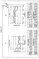
- Fig. 4 is a diagram illustrating the peak gain property as to the frequency of the reception device in the event of employing the antenna device according to the first embodiment.
- Fig. 4 illustrates darkroom properties.
- Fig. 4 illustrates the properties in the FM band and VHF band.
- a curve indicated with H illustrates the property of horizontal polarization (Horizontal Polarization)
- a curve indicated with V illustrates the property of vertical polarization (Vertical Polarization).
- Fig. 4 illustrates charts showing measurement results in detail in accordance with the property diagram.
- Fig. 5 is a diagram illustrating the peak gain property as to the frequency of the reception device in the case of employing the second power supply cord and the high-frequency signal cable bundled at the antenna device according to the present first embodiment.
- Fig. 6 is a diagram illustrating the peak gain property as to the frequency of the reception device in the case of employing the first power supply cord, the second power supply cord, and the high-frequency signal cable bundled at the antenna device according to the present first embodiment.
- Fig. 5 and Fig. 6 illustrate darkroom properties.
- Fig. 5 and Fig. 6 illustrate the properties in the FM and VHF bands.
- a curve indicated with H illustrates the property of horizontal polarization (Horizontal Polarization), and a curve indicated with V illustrates the property of vertical polarization (Vertical Polarization).
- Fig. 5 and Fig. 6 illustrate charts showing measurement results in detail in accordance with the property diagram.
- Fig. 7 is a diagram illustrating a specific configuration example of the antenna device according to the second embodiment of the present invention.
- An antenna device 10A according to the present second embodiment differs from the antenna device 10 according to the first embodiment in that the high frequency blocking portions are replaced with chip components for high-frequency isolation instead of the ferrite cores.
- the first power supply cord 21 is split into two split power supply cord 211 and 212, and one edge of the split power supply cord 211, and one edge of the split power supply cord 212 are connected at a chip board 43 via a core wire and a shield portion.
- This chip board 43 has the same function as the ferrite core 41 according to the first embodiment.
- the core wire and shield portion of the other edge of the split power supply cord 211 are connected to a first connection pattern portion 112A of an antenna element 110A.
- the core wire and shield portion of an edge portion of the second power supply cord 22 are connected to a second round pattern portion 1123A of the antenna element 110A.
- the second round pattern portion 1123A of this antenna element 110A is converted into a chip board.
- This second round pattern portion 1123A has the same function as the function of the ferrite core 42 according to the first embodiment.
- round pattern portions 431, 432, 433, and 434 for connection are formed.
- the round pattern portions 431 and 432 are connected via a filter F441.
- the round pattern portions 433 and 434 are connected via a filter F442.
- a core wire 201 of one edge portion of the split power supply cord 211 is connected to the round pattern portion 431, and a core wire 201 of an edge portion of the split power supply cord 212 is connected to the round pattern portion 432.
- a shield portion 203 of one edge portion of the split power supply cord 211 is connected to the round pattern portion 433, and a shield portion 203 of an edge portion of the split power supply cord 212 is connected to the round pattern portion 434.
- the extended pattern portion 1121A, first round pattern portion 1122A, and second round pattern portion 1123A of the first connection pattern portion 112A are extended to a base edge portion facing the base pattern portion 111.
- Four round pattern portions 1124, 1125, 1126, and 1127 are formed as the second round pattern portion 1123A.
- An edge portion of the extended pattern portion 1121A, and the first round pattern portion 1122A are connected via a filter F112.
- the round pattern portion 1124 and round pattern portion 1125 are connected via a filter F113.
- the round pattern portion 1126 and round pattern portion 1127 are connected via a filter F114.
- the first round pattern portion 1122A and round pattern portion 1126 are connected via the capacitor C111.
- the core wire 201 of the other edge portion of the split power supply cord 211 is connected to the round pattern portion 1124, and the core wire 201 of an edge portion of the second power supply cord 22 is connected to the round pattern portion 1125.
- the shield portion 203 of the other edge portion of the split power supply cord 211 is connected to the round pattern portion 1126, and the shield portion 203 of an edge portion of the second power supply cord 22 is connected to the round pattern portion 1127.
- Fig. 8 is a diagram illustrating a specific configuration example of the antenna device according to the third embodiment of the present invention.
- An antenna device 10B according to the present third embodiment differs from the antenna device 10 according to the first embodiment in that a cord made up of parallel two wires is used as a power supply cord 20B instead of a coaxial cable.
- the power supply cord 20B includes two parallel wires 213 and 214.
- two round pattern portions 1123 on the tip side of the first connection pattern portion 112B are formed so as to connect the two parallel wires 213 and 214 at the antenna element 110B.
- round pattern portions 11231 and 11232 are formed.
- the parallel wire 213 of a first power supply cord 21B is connected to one edge portion of the round pattern portion 11231, and the parallel wire 214 of the first power supply cord 21B is connected to one edge portion of the round pattern portion 11232.
- the parallel wire 213 of a second power supply cord 22B is connected to the other edge portion of the round pattern portion 11231, and the parallel wire 214 of the second power supply cord 22B is connected to the other edge portion of the round pattern portion 11232.
- the other configurations are the same as those in the first embodiment. According to the present third embodiment, the same advantage as with the above-mentioned first embodiment can be obtained.
- Fig. 9 is a diagram illustrating the entire configuration of an antenna device according to the fourth through seventh embodiments of the present invention.
- the antenna device 10C is formed as a power supply cable antenna wherein a high-frequency signal is superimposed, a power supply cable between high-frequency blocking portions thereof is taken as an antenna, and an electric wire and a high-frequency signal line can separately be input to an electronic device.
- the antenna device 10C is formed as a power supply cable antenna for two-frequency common use which is made up of an antenna that another board forms connected to one of the high-frequency blocking portions via a filter, and an antenna made up of the other high-frequency blocking portion different from the above.
- the antenna device 10C is formed as a power supply cable antenna whereby, at the time of connection from an electric wire to a high-frequency power supply circuit portion, a high-frequency current can be blocked by a high-frequency blocking portion, for example, by attaching ferrite beads, an inductor, and a ferrite core.
- the antenna device 10C includes a power supply cord 20 serving as a power transmission cable formed of a coaxial wire or parallel two wires, a high-frequency signal cable (high-frequency signal line) 30, a ferrite core 41 serving as a high-frequency blocking portion 40, and a mold portion 50' including a relay connecting portion
- a car plug 60 for connecting to an onboard power supply unit (power supply unit) is connected to one edge side of the power supply cord 20, and a power supply connector 70 for connecting to the power supply unit of an electronic device is connected to the other edge side.
- a high-frequency handling plug 80 which can be connected to an antenna connecting portion of an electronic device is connected to one edge portion of the high-frequency signal cable 30.
- Fig. 9 only one of the ferrites serving as two high-frequency blocking portions is shown in the drawing.
- the ferrite serving as the other high-frequency blocking portion is disposed within the mold portion 50'.
- the power supply cord 20 is split into a first power supply cord 21 to which the car plug 60 is connected at the mold portion 50', and a second power supply cord 22 to which the power supply connector 70 is connected.
- the mold portion 50' has a configuration so as to fix the shape.
- the first power supply cord 21 and the second power supply cord 22 are disposed within the mold portion 50' so as to be generally orthogonal in a basically extended state as shown in Fig. 9 .
- the second power supply cord 22 and the high-frequency signal cable 30 are disposed within the mold portion 50' so as to be in parallel.
- the mold portion 50' has, for example, as shown in Fig., 9 , a size of width 35 mm and length 200 mm.
- a ferrite core 41 for high-frequency isolation is inserted into a point of 1 m through 1.3 m from the edge portion of the mold portion 50' in the middle of the first power supply cord 21 from the edge portion (right edge in the drawing) of the mold portion 50' to the car plug 60 to receive a VHF low (LOW) band.
- VHF low LOW
- Fig. 10 is a diagram illustrating a specific configuration example of an antenna device according to the fourth embodiment of the present invention.
- An antenna board portion 100 is disposed within the mold portion 50'. With the antenna board portion 100, an antenna element (first antenna element) 110C, and antenna ground (second antenna element) 120 are formed so as to be in parallel.
- the antenna element 110C is formed as a pattern making up a generally U-letter shape. Specifically, the antenna element 110C includes a base pattern portion 111. The length of the base pattern portion 111 is set to 40 mm, for example.
- a first connection pattern portion 112 formed so as to extend orthogonal to the base pattern portion 111 is formed on one edge portion of the base pattern portion 111.
- a first round pattern portion 1122 is formed via a capacitor C111 on the tip portion side of the extended pattern portion 1121 thereof.
- a second round pattern portion 1123 for connecting to the power supply cord 20 via the filter F111 is formed as to the first round pattern portion 1122.
- the capacity of the capacitor C111 is set to 1000 pF, for example.
- the second round pattern portion 1123 is connected to the shield portion 203 of the portion of which the external insulator 204 of the power supply cord 20 has been removed. Note that the length of the extended pattern portion 1121 is set to 20 mm, for example.
- a second connection pattern portion 113 formed so as to extend orthogonal to the base pattern portion 111 is formed on the other edge portion of the base pattern portion 111.
- a round pattern portion 1132 is formed via a matching element, e.g., an inductor L111 on the tip portion side of the extended pattern portion 1131.
- the inductance of the inductor L111 is set to 40 nH, for example.
- the core wire 301 of the high-frequency signal cable 30 is connected to the round pattern portion 1132.
- the antenna ground 120 is formed in a tabular shape so as to be in parallel with the antenna element 110C (left side in Fig. 10 ).
- the antenna ground 120 is formed with a size of width 30 mm and length 150 mm, for example.
- the power supply cord 20 is, as described above, split into the first power supply cord 21 and the second power supply cord 22.
- the external insulator 204 is removed.
- another ferrite core 42 serving as the high-frequency blocking portion 40, not shown in Fig. 9 , is disposed.
- a coaxial wire is used as the power supply cord 20.
- a ferrite core 41 is disposed (inserted) in the split first power supply cord 21, and a ferrite core 42 is disposed (inserted) in the second power supply cord 22.
- the disposed position of the ferrite core 41 is adjusted with length of around 1 m through 1.3 m to shift resonance to the FM band that is the LOW band of VHF, as described above, so as to resonate with a lower frequency than the antenna made up of the antenna board portion 100.
- the external insulator 204 has been removed at the spilt portion 23 immediately before the ferrite core 42 disposed in the second power supply cord 22 between the ferrite cores 41 and 42 serving as the two high-frequency blocking portions 40.
- the shield portion 203 of this split portion 23 is then connected to the second round pattern portion 1123 on the antenna element 110C side, and a first antenna is formed.
- a second antenna 12 made up of the antenna board portion 100 is formed of an antenna device 110C and antenna ground 120.
- the antenna device 10C is configured so as to receive digital television broadcast waves broadcasted with the UHF band.
- a dipole antenna 30 cm with 15 cm each side is required, but the size of the mold portion 50 increases. Therefore, with the present fourth embodiment, an arrangement is employed wherein the antenna ground 120 is secured, the antenna element 110C is shortened, and input impedance is adjusted at the inductor L111 which is a matching element.
- inductance is 47 nH, but high antenna performance is maintained without deteriorating antenna gain by increasing antenna radiation at the antenna ground 120.
- the second antenna 12 and first antenna 11 are connected via the filter F111 which exhibits low impedance with the VHF band, and exhibits high impedance with the UHF band so as to separate the first antenna 11 and second antenna 12. Moreover, as electrostatic countermeasures, with the VHF and UHF bands, the first antenna 11 and second antenna 12 are corrected via the capacitor C111 which exhibits low impedance.
- the power feeding portion of the second antenna 12 is a portion where the antenna ground 120 is connected to the shield portion 303 of the high-frequency signal cable 30 which is a coaxial wire, and the core wire 301 portion of the coaxial wire is connected to the round pattern portion 1132 of the antenna element 110C.
- the high-frequency signal cable 30 is connected to the set (electronic device) via the high-frequency handling plug 80.
- the antenna board portion 100 and the above-mentioned connecting portions are stored in the mold portion 50'.
- FIG. 11 are diagrams illustrating the peak gain property as to the frequency of the reception device in the event of employing the antenna device according to the present fourth embodiment.
- (A) and (B) in Fig. 11 illustrate darkroom properties.
- (A) in Fig. 11 illustrates the properties in the FM and VHF bands
- (B) in Fig. 11 illustrates the property in the UHF band.
- a curve indicated with H illustrates the property of horizontal polarization (Horizontal Polarization)
- a curve indicated with V illustrates the property of vertical polarization (Vertical Polarization).
- FIG. 11 illustrate charts showing measurement results in detail in accordance with the property diagram.
- FIG. 12 are diagrams illustrating the peak gain property as to the frequency of the reception device in the event of employing the second power supply cord and the high-frequency signal cable bundled at the antenna device according to the present fourth embodiment.
- Fig. 14 is a diagram illustrating a specific configuration example of the antenna device according to the fifth embodiment of the present invention.
- An antenna device 10D according to the present fifth embodiment differs from the antenna device 10C according to the fourth embodiment in that the high frequency blocking portions are replaced with chip components for high-frequency isolation instead of the ferrite cores.
- the first power supply cord 21 is split into two split power supply cord 211 and 212, and one edge of the split power supply cord 211, and one edge of the split power supply cord 212 are connected at the chip board 43 via a core wire and a shield portion.
- This chip board 43 has the same function as the ferrite core 41 according to the fourth embodiment.
- the core wire and shield portion of the other edge of the split power supply cord 211 are connected to a first connection pattern portion 112D of an antenna element 110D of an antenna board portion 100D.
- the core wire and shield portion of an edge portion of the second power supply cord 22 are connected to a second round pattern portion 1123D of the antenna element 110D.
- the second round pattern portion 1123D of this antenna element 110D is converted into a chip board.
- This second round pattern portion 1123D has the same function as the function of the ferrite core 42 according to the fourth embodiment.
- round pattern portions 431, 432, 433, and 434 for connection are formed.
- the round pattern portions 431 and 432 are connected via a filter F431.
- the round pattern portions 433 and 434 are connected via a filter F432.
- a core wire 201 of one edge portion of the split power supply cord 211 is connected to the round pattern portion 431, and a core wire 201 of an edge portion of the split power supply cord 212 is connected to the round pattern portion 432.
- a shield portion 203 of one edge portion of the split power supply cord 211 is connected to the round pattern portion 433, and a shield portion 203 of an edge portion of the split power supply cord 212 is connected to the round pattern portion 434.
- the extended pattern portion 1121D, first round pattern portion 1122D, and second round pattern portion 1123D of the first connection pattern portion 112D are extended to a base edge portion facing the base pattern portion 111.
- Four round pattern portions 1124, 1125, 1126, and 1127 are formed as the second round pattern portion 1123D.
- An edge portion of the extended pattern portion 1121D, and the first round pattern portion 1122D are connected via the filter F112.
- the round pattern portion 1124 and round pattern portion 1125 are connected via the filter F113.
- the round pattern portion 1126 and round pattern portion 1127 are connected via the filter F114.
- the first round pattern portion 1122D and round pattern portion 1126 are connected via the capacitor C111.
- the core wire 201 of the other edge portion of the split power supply cord 211 is connected to the round pattern portion 1124, and the core wire 201 of an edge portion of the second power supply cord 22 is connected to the round pattern portion 1125.
- the shield portion 203 of the other edge portion of the split power supply cord 211 is connected to the round pattern portion 1126, and the shield portion 203 of an edge portion of the second power supply cord 22 is connected to the round pattern portion 1127.
- the other configurations are the same as those in the fourth embodiment. According to the present fifth embodiment, the same advantage as with the above-mentioned fourth embodiment can be obtained.
- Fig. 15 is a diagram illustrating a specific configuration example of the antenna device according to the sixth embodiment of the present invention.
- An antenna device 10E according to the present sixth embodiment differs from the antenna device 10C according to the fourth embodiment in that a cord made up of parallel two wires is used as a power supply cord 20E instead of a coaxial cable.
- the power supply cord 20E includes two parallel wires 213 and 214.
- two round pattern portions 1123 on the tip side of the first connection pattern portion 112E are formed so as to connect the two parallel wires 213 and 214 at the antenna element 110E.
- round pattern portions 11231 and 11232 are formed.
- the parallel wire 213 of a first power supply cord 21E is connected to one edge portion of the round pattern portion 11231, and the parallel wire 214 of the first power supply cord 21E is connected to one edge portion of the round pattern portion 11232.
- the parallel wire 213 of a second power supply cord 22E is connected to the other edge portion of the round pattern portion 11231, and the parallel wire 214 of the second power supply cord 22E is connected to the other edge portion of the round pattern portion 11232.
- the other configurations are the same as those in the fourth embodiment. According to the present sixth embodiment, the same advantage as with the above-mentioned fourth embodiment can be obtained.
- Fig. 16 is a diagram illustrating a specific configuration example of the antenna device according to the seventh embodiment of the present invention.
- An antenna device 10F according to the present seventh embodiment differs from the antenna device 10C according to the fourth embodiment in that this antenna device is formed as a dipole antenna at an antenna board portion 100F.
- a first antenna element 130 and a second antenna element 140 are formed on the antenna board portion 100F. Note that it is desirable to set the lengths of the first antenna element 130 and second antenna element 140 to 30 cm with 15 cm each side.
- a first connection pattern portion 132 formed so as to extend orthogonal to the base pattern portion 131 is formed on one edge portion of the base pattern portion 131.
- a first round pattern portion 1322 is formed via a filter F131 on the tip portion side of the extended pattern portion 1321 thereof.
- Two second round pattern portions 1323 and 1324 for connecting to the power supply cord 20 via a capacitor C131 are formed as to the first round pattern portion 1322.
- the capacity of the capacitor C131 is set to 1000 pF, for example.
- the second round pattern portion 1323 is connected to the shield portion 203 of the portion of which the external insulator 204 of the power supply cord 20 has been removed.
- a second connection pattern portion 133 formed so as to extend orthogonal to the base pattern portion 131 is formed on one edge portion of the base pattern portion 131.
- a bent pattern portion 1332 extended bent toward the second antenna element 140 side is formed on the tip portion side of the extended pattern portion 1331.
- a round pattern portion 1333 is formed facing the bent pattern portion 1332.
- a third connection pattern portion 142 formed so as to extend orthogonal to the base pattern portion 141 is formed on one edge portion of the base pattern portion 141.
- a fourth connection pattern portion 143 formed so as to extend orthogonal to the base pattern portion 141 is formed on the other edge portion of the base pattern portion 141.
- a bent pattern portion 1432 extended bent on the first antenna element 130 side is formed on the tip portion of the extended pattern portion 1431.
- a round pattern portion 1433 is formed facing the bent pattern portion 1432.
- the shield portion 203 of the first power supply cord 21 is connected to one edge portion of the second round pattern portion 1323 of the first antenna element 130, and the core wire 201 of the first power supply cord 21 is connected to one edge portion of the second round pattern portion 1324.
- the shield portion 203 of the second power supply cord 22 is connected to the other edge portion of the second round pattern portion 1323 of the first antenna element 130, and the core wire 201 of the second power supply cord 22 is connected to the other edge portion of the second round pattern portion 1324.
- the core wire 301 of the high-frequency signal cable 30 is connected to the round pattern portion 1333.
- the shield portion 303 of the high-frequency signal cable 30 is connected to the round pattern portion 1433.
- the bend pattern portion 1332 and round pattern portion 1333 of the second connection pattern portion 133, and the bent pattern portion 1432 and round pattern portion 1433 of the fourth connection pattern portion 143 are connected to a balanced-to-unbalanced transformer (balun) 150.
- FIG. 17 are diagrams illustrating the peak gain property as to the frequency of the reception device in the event of employing the antenna device according to the present seventh embodiment.
- (A) in Fig. 17 illustrates the properties in the FM and VHF bands
- (B) in Fig. 17 illustrates the property in the UHF band.
- a curve indicated with H illustrates the property of horizontal polarization (Horizontal Polarization)
- a curve indicated with V illustrates the property of vertical polarization (Vertical Polarization).
- FIG. 17 illustrate charts showing measurement results in detail in accordance with the property diagram.
- the antenna device directly connects the shield portion 203 of the power supply cord 20, and the core wire 301 of the high-frequency signal cable 30 at the antenna board portion 100 of the connecting portion though not shown in the drawing. Note that, in this case, it is desirable to connect the shield portion 203 of the power supply cord 20, and the core wire 301 of the high-frequency signal cable 30 via a capacitor.
- reception of FM that is an FM-VICS band, and reception of the UHF band for receiving a digital television broadcast can be performed without problems.
- broadcast waves can be received with a sufficiently wide frequency band and sufficient gain just by connecting wire materials even if used bundled without complicated efforts, and suitable reception sensitivity can be obtained.
- the reception sensitivity of the set improves 5 to 10 dB or so as compared to a conventional device, and accordingly, the reception sensitivity greatly improves (improvement of 5 to 10 dB over the conventional).
- the configuration is simple, manufacturing can be performed with low cost, and attachment can readily be performed. Also, influence of the set is not readily received.
- the antenna of the antenna device according to the present invention greatly differs from a film antenna principally used for mounting a conventional antenna device on a vehicle.
- the antenna element on the film side is adhered to the front glass of the vehicle, and also, the GND of a coaxial wire is connected to the body of the vehicle since the body of a vehicle is commonly used as GND necessary for serving as an antenna.
- the film antenna serves as an antenna using the antenna element of the film, and the GND of the body of the vehicle, and electric waves received at the antenna thereof are input to a reception device.
- a prominent feature of the antenna device according to the present invention is its difference from the above-mentioned film antenna in that the power supply cord and the antenna element are shared by using a portion of the power supply cord (e.g., in the case of a cord using a shield wire, a portion thereof obtained by separating high-frequency current flowing on the surface thereof using a ferrite having great high-frequency impedance) as an antenna element instead of the antenna element of a film.
- the antenna device according to the present invention differs from the above-mentioned film antenna in that the antenna GND (antenna ground 120) of the board is served as an antenna instead of the body of the vehicle being used as GND.
- the first through third embodiments including no antenna board portion differ from the above-mentioned film antenna in that the GND of the reception device, and the GND (shield portion 203) of the outer cover of the coaxial wire are used instead of using the body of the vehicle as GND.
- the antenna of the antenna device according to the present invention differs from a conventional film antenna, the user does not have to adhere a film antenna onto the front glass, and accordingly, convenience is high.
- the antenna element such as the outer cover of the power supply cord is used for reception of the VHF band, and connected via a filter element (filter F111) which exhibits low impedance with the VHF band, and also exhibits high impedance with the UHF band, and thus, an antenna for two-frequency common use which receives the UHF band at the antenna board portion, and receives the VHF band at the antenna board portion and the antenna element of the power supply cord portion is realized.
- filter F111 filter element which exhibits low impedance with the VHF band, and also exhibits high impedance with the UHF band
Abstract
Description
- The present invention relates to an antenna device which receives electric waves using a power supply cord for power supply.
- In recent years, tuners whereby high-definition (HD) television video can be viewed have come to be included even in notebook personal computers (PC) and small televisions, and there is increased demand to be able to view television pictures from anywhere even within a room where a user wants to receive.
Also, examples of electronic devices having television functions include small electronic devices such as PNDs (Personal Navigation Devices) and so forth, besides cellular phones and notebook PCs. - Cellular phones and so forth which can receive digital television broadcasts and radio broadcasts receive broadcast waves at an internal antenna or external antenna. Here, internal antennas have an advantage in that the design of the cellular phone is not compromised.
However, internal antennas have a disadvantage in that sensitivity deteriorates as compared to external antennas, influence of internal noise can readily be received, and so forth. - On the other hand, examples of external antennas include rod antennas. Rod antennas have features wherein sensitivity and so forth excel as compared to internal antennas.
However, rod antennas have a disadvantage such that the design of the electronic device such as a cellular phone or the like is compromised, and further the antenna protrudes. - With regard to external antennas, it has been proposed in
PTLs 1 through 5 and so forth for a power supply cord to be used as an antenna.
An antenna device using this power supply cord can receive electric wave signals of the FM band transmitted from a broadcast station, and a VHF band through a UHF band used for receiving a digital television broadcast. -
- PTL 1: Japanese Unexamined Patent Application Publication No.
2005-341067 - PTL 2: Japanese Unexamined Patent Application Publication No.
2002-151932 - PTL 3: Japanese Unexamined Patent Application Publication No.
2001-274704 - PTL 4: Japanese Unexamined Patent Application Publication No.
2001-168982 - PTL 5: Japanese Unexamined Patent Application Publication No.
2005-136907 - However, the proposed antenna devices using a power supply cord may not be able to receive broadcast waves with a sufficiently wide frequency band and sufficient gain.
Also, the sensitivity of the proposed antenna devices using a power supply cord changes in the case of bundling wire materials, and accordingly, in the case of using such an antenna device, a troublesome operation of unbundling the wire materials to obtain excellent reception sensitivity may be incurred. - Accordingly, in the case of including this antenna device, e.g., a PND, on a vehicle, the user has no other choice but to use a glass antenna on which a front glass is adhered, to obtain excellent reception sensitivity, given the current situation.
However, it is difficult for a common user to easily apply glass antennas, so convenience is poor. - The present invention provides an antenna device which can receive broadcast waves with a sufficiently wide frequency band and sufficient gain just by connecting wire material even if used bundled, without complicated efforts, and can obtain suitable reception sensitivity.
- An antenna device includes a power supply cord which can transmit power, a connecting portion, a high-frequency signal cable for extracting a high-frequency signal from the connecting portion, and a high-frequency blocking portion disposed in two places in the length direction of the power supply cord, and with the power supply cord, a portion between the two high-frequency blocking portions is connected to the connecting portion to form an antenna, and the high-frequency signal cable is connected to the power supply cord via the connecting portion.
- According to the present invention, broadcast waves can be received with a sufficiently wide frequency band and sufficient gain just by connecting wire material even if used bundled, without complicated efforts, and suitable reception sensitivity can be obtained.
-
- [
Fig. 1] Fig. 1 is a diagram illustrating the entire configuration of an antenna device according to first through third embodiments of the present invention. - [
Fig. 2] Fig. 2 is a diagram illustrating a specific configuration example of the antenna device according to the first embodiment of the present invention. - [
Fig. 3] Fig. 3 is a diagram illustrating a configuration example of a coaxial cable with a shield portion. - [
Fig. 4] Fig. 4 is a diagram illustrating the peak gain property as to the frequency of a reception device in the event of employing the antenna device according to the present first embodiment. - [
Fig. 5] Fig. 5 is a diagram illustrating the peak gain property as to the frequency of a reception device in the event of employing a second power supply cord and a high-frequency signal cable bundled at the antenna device according to the present first embodiment. - [
Fig. 6] Fig. 6 is a diagram illustrating the peak gain property as to the frequency of a reception device in the event of employing the first power supply cord, the second power supply cord, and the high-frequency signal cable bundled at the antenna device according to the present first embodiment. - [
Fig. 7] Fig. 7 is a diagram illustrating a specific configuration example of the antenna device according to the second embodiment of the present invention. - [
Fig. 8] Fig. 8 is a diagram illustrating a specific configuration example of the antenna device according to the third embodiment of the present invention. - [
Fig. 9] Fig. 9 is a diagram illustrating the entire configuration of an antenna device according to fourth through seventh embodiments of the present invention. - [
Fig. 10] Fig. 10 is a diagram illustrating a specific configuration example of the antenna device according to the fourth embodiment of the present invention. - [
Fig. 11] Fig. 11 is a diagram illustrating the peak gain property as to the frequency of a reception device in the event of employing the antenna device according to the present fourth embodiment. - [
Fig. 12] Fig. 12 is a diagram illustrating the peak gain property as to the frequency of a reception device in the event of employing a second power supply cord and a high-frequency signal cable bundled at the antenna device according to the present fourth embodiment. - [
Fig. 13] Fig. 13 is a diagram illustrating the peak gain property as to the frequency of a reception device in the event of employing the first power supply cord, the second power supply cord, and the high-frequency signal cable bundled at the antenna device according to the present fourth embodiment. - [
Fig. 14] Fig. 14 is a diagram illustrating a specific configuration example of the antenna device according to the fifth embodiment of the present invention. - [
Fig. 15] Fig. 15 is a diagram illustrating a specific configuration example of the antenna device according to the sixth embodiment of the present invention. - [
Fig. 16] Fig. 16 is a diagram illustrating a specific configuration example of the antenna device according to the seventh embodiment of the present invention. - [
Fig. 17] Fig. 17 is a diagram illustrating the peak gain property as to the frequency of a reception device in the event of employing the antenna device according to the present seventh embodiment. - Description will be made below by correlating embodiments of the present invention with drawings.
Note that description will be made in accordance with the following sequence. - 1. First Embodiment (First Configuration Example of Antenna Device)
- 2. Second Embodiment (Second Configuration Example of Antenna Device)
- 3. Third Embodiment (Third Configuration Example of Antenna Device)
- 4. Fourth Embodiment (Fourth Configuration Example of Antenna Device)
- 5. Fifth Embodiment (Fifth Configuration Example of Antenna Device)
- 6. Sixth Embodiment (Sixth Configuration Example of Antenna Device)
- 7. Seventh Embodiment (Seventh Configuration Example of Antenna Device)
- 8. Eighth Embodiment (Eighth Configuration Example of Antenna Device)
- An antenna device which can be applied to an electronic device such as an onboard PND or the like will be described below as an example.
-
Fig. 1 is a diagram illustrating the entire configuration of an antenna device according an embodiment of the present invention. - With an
antenna device 10 according to the present embodiment, two high-frequency blocking portions are disposed in a portion of an electric wire for power transmission or an electric wire in parallel therewith.
Theantenna device 10 is formed as a power supply cable antenna wherein a high-frequency signal is superimposed, a power supply cable between high-frequency blocking portions thereof is taken as an antenna, and an electric wire and a high-frequency signal line can separately be input to an electronic device.
Theantenna device 10 is formed as a power supply cable antenna for two-frequency common use which is made up of an antenna that another board forms connected to one of the high-frequency blocking portions via a filter, and an antenna made up of the other high-frequency blocking portion different from the above.
Theantenna device 10 is formed as a power supply cable antenna whereby, at the time of connection from an electric wire to a high-frequency power supply circuit portion, a high-frequency current can be blocked by a high-frequency blocking portion, for example, by attaching ferrite beads, an inductor, and a ferrite core. - The
antenna device 10 according to the present embodiment includes apower supply cord 20 serving as a power transmission cable formed of a coaxial wire or parallel two wires, a high-frequency signal cable (high-frequency signal line) 30, aferrite core 41 serving as a high-frequency blocking portion 40, and amold portion 50 serving as a connecting portion.
Also, with theantenna device 10, acar plug 60 for connecting to an onboard power supply unit (power supply unit) is connected to one edge side of thepower supply cord 20, and apower supply connector 70 for connecting to the power supply unit of an electronic device is connected to the other edge side.
Also, a high-frequency handling plug 80 which can be connected to an antenna connecting portion of an electronic device is connected to one edge portion of the high-frequency signal cable 30. - Note that, in
Fig. 1 , only one of the ferrites serving as two high-frequency blocking portions is shown in the drawing. The ferrite serving as the other high-frequency blocking portion is disposed within themold portion 50. - The
power supply cord 20 is split into a firstpower supply cord 21 to which thecar plug 60 is connected at themold portion 50, and a secondpower supply cord 22 to which thepower supply connector 70 is connected.
Themold portion 50 has a configuration capable of fixing the shape.
The firstpower supply cord 21 and the secondpower supply cord 22 are basically disposed within themold portion 50 so as to be generally orthogonal in an extended state as shown inFig. 1 .
Also, the secondpower supply cord 22 and the high-frequency signal cable 30 are disposed within themold portion 50 so as to be in parallel. - A
ferrite core 41 for high-frequency isolation is inserted into a point of 1 m through 1.3 m from the edge portion of themold portion 50 in the middle of the firstpower supply cord 21 from the edge portion (right edge in the drawing) of themold portion 50 to thecar plug 60 to receive a VHF low band. -
Fig. 2 is a diagram illustrating a specific configuration example of an antenna device according to the first embodiment of the present invention. - With the present first embodiment, a specific configuration within the
mold portion 50 is shown.
Also, with the present first embodiment, a coaxial wire is applied as thepower supply cord 20. A configuration example of thispower supply cord 20 will be described. -
Fig. 3 is a diagram illustrating a configuration example of a coaxial cable with a shield portion. - A
coaxial cable 200 includes multiplecore wires 201 and aninternal insulator 202 for insulating thecore wires 201.
Thecoaxial cable 200 includes ashield portion 203 disposed in the outer circumference of theinternal insulator 202, and an external insulator (outer cover, jacket) 204 such as elastomer for covering the entire outer circumference, or the like.
With thecore wires 201, the outer circumferences are covered and insulated by aflame resistance insulator 205.
Also, theshield portion 203 is formed of an annealed copper wire, for example.
Also, theshield portion 203 is formed of multiple wires having electro-conductivity, e.g., a tactical grouped shield obtained by tactically grouping bare copper wires.
Note that, with the tactical grouped shield, occurrence of a shield gap is less even at the time of bending as compared to spiral shield, and this shield is known as an electrostatic shield method having suitable flexibility, bending strength, and mechanical strength.
Thecore wires 201 and theshield portion 203 have high-frequency impedance. - Note that the high-
frequency signal cable 30 is formed of a coaxial cable (coaxial wire), and basically has the same configuration as the above-mentioned coaxial cable with a shield portion.
Specifically, the high-frequency signal cable 30 includes acore wire 301, and aninternal insulator 302 for insulating thecore wire 301.
The high-frequency signal cable 30 includes ashield portion 303 disposed in the outer circumference of theinternal insulator 302, and an external insulator (outer cover, jacket) 304 such as elastomer for covering the entire outer circumference, or the like. - An
antenna element 110 is disposed within themold portion 50. - The
antenna element 110 is formed as a pattern making up a generally U-letter shape.
Specifically, theantenna element 110 includes abase pattern portion 111. - With the
antenna element 110, a firstconnection pattern portion 112 formed so as to extend orthogonal to thebase pattern portion 111 is formed on one edge portion of thebase pattern portion 111.
With the firstconnection pattern portion 112, around pattern portion 1123 for connecting to thepower supply cord 20 via a capacitor C111 is formed on the tip portion side of theextended pattern portion 1121.
The capacity of the capacitor C111 is set to 1000 pF, for example.
Theround pattern portion 1123 is connected to theshield portion 203 of the portion of which theexternal insulator 204 of thepower supply cord 20 has been removed. - With the
antenna element 110, a secondconnection pattern portion 113 formed so as to extend orthogonal to thebase pattern portion 111 is formed on the other edge portion of thebase pattern portion 111.
Thecore wire 301 of the high-frequency signal cable 30 is connected to the secondconnection pattern portion 113. - The
power supply cord 20 is, as described above, split into the firstpower supply cord 21 and the secondpower supply cord 22.
At thesplit portion 23 between the firstpower supply cord 21 and the secondpower supply cord 22, theexternal insulator 204 is removed.
Near thesplit portion 23 where theexternal insulator 204 of the secondpower supply cord 22 has been removed, i.e., at the edge portion on the opposite side of the connection edge of thepower supply connector 70 of the secondpower supply cord 22, anotherferrite core 42 serving as the high-frequency blocking portion 40, not shown inFig. 1 , is disposed. - In this way, with the
antenna device 10 according to the present first embodiment, a coaxial wire is used as thepower supply cord 20.
With thepower supply cord 20, aferrite core 41 is disposed (inserted) in the split firstpower supply cord 21, and aferrite core 42 is disposed (inserted) in the secondpower supply cord 22.
The disposed position of theferrite core 41 is adjusted with length of around 1 m through 1.3 m to shift resonance to the FM band that is the low band of VHF, as described above. - With the
power supply cord 20, theexternal insulator 204 has been removed at the spiltportion 23 immediately before theferrite core 42 disposed in the secondpower supply cord 22 between theferrite cores frequency blocking portions 40.
Theshield portion 203 of thissplit portion 23 is then connected to theround pattern portion 1123 on theantenna element 110 side, and an antenna is formed. - The
antenna device 10 according to the present embodiment is configured so as to perform at least reception of FM that is an FM-VICS band.
The capacitor C111 is connected between thepower supply cord 20 and the high-frequency signal cable as electrostatic countermeasures. - With the antenna feeding portion thus formed, the core wire 310 portion of the high-
frequency signal cable 30 which is a coaxial wire is a portion connected to the secondconnection pattern portion 113 of theantenna element 110.
The high-frequency signal cable 30 is then connected to the set (electronic device) via the high-frequency handling plug 80. - The
antenna element 110 and the above connecting portions are stored in themold portion 50. -
Fig. 4 is a diagram illustrating the peak gain property as to the frequency of the reception device in the event of employing the antenna device according to the first embodiment.Fig. 4 illustrates darkroom properties.
Fig. 4 illustrates the properties in the FM band and VHF band.
InFig. 4 , a curve indicated with H illustrates the property of horizontal polarization (Horizontal Polarization), and a curve indicated with V illustrates the property of vertical polarization (Vertical Polarization).
Also,Fig. 4 illustrates charts showing measurement results in detail in accordance with the property diagram. - As can be understood from the drawing, with darkroom properties, reception of FM that is an FM-VICS band can be performed without problems.
-
Fig. 5 is a diagram illustrating the peak gain property as to the frequency of the reception device in the case of employing the second power supply cord and the high-frequency signal cable bundled at the antenna device according to the present first embodiment.
Fig. 6 is a diagram illustrating the peak gain property as to the frequency of the reception device in the case of employing the first power supply cord, the second power supply cord, and the high-frequency signal cable bundled at the antenna device according to the present first embodiment.
Fig. 5 andFig. 6 illustrate darkroom properties.
Fig. 5 andFig. 6 illustrate the properties in the FM and VHF bands.
InFig. 5 andFig. 6 , a curve indicated with H illustrates the property of horizontal polarization (Horizontal Polarization), and a curve indicated with V illustrates the property of vertical polarization (Vertical Polarization).
Also,Fig. 5 andFig. 6 illustrate charts showing measurement results in detail in accordance with the property diagram. - In a bundled state as well, as shown in
Fig. 5 andFig. 6 , very excellent results have been obtained despite a slight deterioration.
That is to say, as can be understood from the drawings, even in a bundled state, with darkroom properties, reception of FM that is an FM-VICS band can be performed without problems. -
Fig. 7 is a diagram illustrating a specific configuration example of the antenna device according to the second embodiment of the present invention. - An
antenna device 10A according to the present second embodiment differs from theantenna device 10 according to the first embodiment in that the high frequency blocking portions are replaced with chip components for high-frequency isolation instead of the ferrite cores. - Specifically, with the
antenna device 10A, the firstpower supply cord 21 is split into two splitpower supply cord power supply cord 211, and one edge of the splitpower supply cord 212 are connected at achip board 43 via a core wire and a shield portion.
Thischip board 43 has the same function as theferrite core 41 according to the first embodiment. - Also, the core wire and shield portion of the other edge of the split
power supply cord 211 are connected to a firstconnection pattern portion 112A of anantenna element 110A.
The core wire and shield portion of an edge portion of the secondpower supply cord 22 are connected to a secondround pattern portion 1123A of theantenna element 110A. The secondround pattern portion 1123A of thisantenna element 110A is converted into a chip board.
This secondround pattern portion 1123A has the same function as the function of theferrite core 42 according to the first embodiment. - With the
chip board 43,round pattern portions
Theround pattern portions
Theround pattern portions
Acore wire 201 of one edge portion of the splitpower supply cord 211 is connected to theround pattern portion 431, and acore wire 201 of an edge portion of the splitpower supply cord 212 is connected to theround pattern portion 432.
Ashield portion 203 of one edge portion of the splitpower supply cord 211 is connected to theround pattern portion 433, and ashield portion 203 of an edge portion of the splitpower supply cord 212 is connected to theround pattern portion 434. - With the
antenna element 110A, theextended pattern portion 1121A, firstround pattern portion 1122A, and secondround pattern portion 1123A of the firstconnection pattern portion 112A are extended to a base edge portion facing thebase pattern portion 111.
Fourround pattern portions round pattern portion 1123A. - An edge portion of the
extended pattern portion 1121A, and the firstround pattern portion 1122A are connected via a filter F112.
Theround pattern portion 1124 andround pattern portion 1125 are connected via a filter F113.
Theround pattern portion 1126 andround pattern portion 1127 are connected via a filter F114.
Also, the firstround pattern portion 1122A andround pattern portion 1126 are connected via the capacitor C111. - The
core wire 201 of the other edge portion of the splitpower supply cord 211 is connected to theround pattern portion 1124, and thecore wire 201 of an edge portion of the secondpower supply cord 22 is connected to theround pattern portion 1125.
Theshield portion 203 of the other edge portion of the splitpower supply cord 211 is connected to theround pattern portion 1126, and theshield portion 203 of an edge portion of the secondpower supply cord 22 is connected to theround pattern portion 1127. - With the present second embodiment, the other configurations are the same as those in the first embodiment.
According to the present second embodiment, the same advantage as with the above-mentioned first embodiment can be obtained. -
Fig. 8 is a diagram illustrating a specific configuration example of the antenna device according to the third embodiment of the present invention. - An
antenna device 10B according to the present third embodiment differs from theantenna device 10 according to the first embodiment in that a cord made up of parallel two wires is used as apower supply cord 20B instead of a coaxial cable.
Thepower supply cord 20B includes twoparallel wires
With theantenna device 10B according to the third embodiment, tworound pattern portions 1123 on the tip side of the firstconnection pattern portion 112B are formed so as to connect the twoparallel wires antenna element 110B.
Specifically,round pattern portions
Theparallel wire 213 of a firstpower supply cord 21B is connected to one edge portion of theround pattern portion 11231, and theparallel wire 214 of the firstpower supply cord 21B is connected to one edge portion of theround pattern portion 11232.
Theparallel wire 213 of a second power supply cord 22B is connected to the other edge portion of theround pattern portion 11231, and theparallel wire 214 of the second power supply cord 22B is connected to the other edge portion of theround pattern portion 11232. - With the present third embodiment, the other configurations are the same as those in the first embodiment.
According to the present third embodiment, the same advantage as with the above-mentioned first embodiment can be obtained. - Next, the fourth through seventh embodiments of the present invention will be described.
Fig. 9 is a diagram illustrating the entire configuration of an antenna device according to the fourth through seventh embodiments of the present invention. - With an
antenna device 10C according to the present embodiment, two high-frequency blocking portions are disposed in a portion of an electric wire for power transmission or an electric wire provided in parallel therewith.
Theantenna device 10C is formed as a power supply cable antenna wherein a high-frequency signal is superimposed, a power supply cable between high-frequency blocking portions thereof is taken as an antenna, and an electric wire and a high-frequency signal line can separately be input to an electronic device.
Theantenna device 10C is formed as a power supply cable antenna for two-frequency common use which is made up of an antenna that another board forms connected to one of the high-frequency blocking portions via a filter, and an antenna made up of the other high-frequency blocking portion different from the above.
Theantenna device 10C is formed as a power supply cable antenna whereby, at the time of connection from an electric wire to a high-frequency power supply circuit portion, a high-frequency current can be blocked by a high-frequency blocking portion, for example, by attaching ferrite beads, an inductor, and a ferrite core. - The
antenna device 10C according to the present embodiment includes apower supply cord 20 serving as a power transmission cable formed of a coaxial wire or parallel two wires, a high-frequency signal cable (high-frequency signal line) 30, aferrite core 41 serving as a high-frequency blocking portion 40, and a mold portion 50' including a relay connecting portion
Also, with theantenna device 10C, acar plug 60 for connecting to an onboard power supply unit (power supply unit) is connected to one edge side of thepower supply cord 20, and apower supply connector 70 for connecting to the power supply unit of an electronic device is connected to the other edge side.
Also, a high-frequency handling plug 80 which can be connected to an antenna connecting portion of an electronic device is connected to one edge portion of the high-frequency signal cable 30. - Note that, in
Fig. 9 , only one of the ferrites serving as two high-frequency blocking portions is shown in the drawing. The ferrite serving as the other high-frequency blocking portion is disposed within the mold portion 50'. - The
power supply cord 20 is split into a firstpower supply cord 21 to which thecar plug 60 is connected at the mold portion 50', and a secondpower supply cord 22 to which thepower supply connector 70 is connected.
The mold portion 50' has a configuration so as to fix the shape.
The firstpower supply cord 21 and the secondpower supply cord 22 are disposed within the mold portion 50' so as to be generally orthogonal in a basically extended state as shown inFig. 9 .
Also, the secondpower supply cord 22 and the high-frequency signal cable 30 are disposed within the mold portion 50' so as to be in parallel. - The mold portion 50' has, for example, as shown in
Fig., 9 , a size ofwidth 35 mm andlength 200 mm.
Aferrite core 41 for high-frequency isolation is inserted into a point of 1 m through 1.3 m from the edge portion of the mold portion 50' in the middle of the firstpower supply cord 21 from the edge portion (right edge in the drawing) of the mold portion 50' to thecar plug 60 to receive a VHF low (LOW) band. -
Fig. 10 is a diagram illustrating a specific configuration example of an antenna device according to the fourth embodiment of the present invention. - With the present fourth embodiment, a specific configuration within the mold portion 50' is shown.
Also, with the present fourth embodiment, a coaxial wire is applied as thepower supply cord 20. A configuration example of thispower supply cord 20 is the same as with the above-mentionedFig. 3 . - An
antenna board portion 100 is disposed within the mold portion 50'.
With theantenna board portion 100, an antenna element (first antenna element) 110C, and antenna ground (second antenna element) 120 are formed so as to be in parallel. - The
antenna element 110C is formed as a pattern making up a generally U-letter shape.
Specifically, theantenna element 110C includes abase pattern portion 111.
The length of thebase pattern portion 111 is set to 40 mm, for example. - With the
antenna element 110C, a firstconnection pattern portion 112 formed so as to extend orthogonal to thebase pattern portion 111 is formed on one edge portion of thebase pattern portion 111.
With the firstconnection pattern portion 112, a firstround pattern portion 1122 is formed via a capacitor C111 on the tip portion side of theextended pattern portion 1121 thereof. A secondround pattern portion 1123 for connecting to thepower supply cord 20 via the filter F111 is formed as to the firstround pattern portion 1122. The capacity of the capacitor C111 is set to 1000 pF, for example.
The secondround pattern portion 1123 is connected to theshield portion 203 of the portion of which theexternal insulator 204 of thepower supply cord 20 has been removed.
Note that the length of theextended pattern portion 1121 is set to 20 mm, for example. - With the
antenna element 110C, a secondconnection pattern portion 113 formed so as to extend orthogonal to thebase pattern portion 111 is formed on the other edge portion of thebase pattern portion 111.
With the secondconnection pattern portion 113, around pattern portion 1132 is formed via a matching element, e.g., an inductor L111 on the tip portion side of theextended pattern portion 1131. The inductance of the inductor L111 is set to 40 nH, for example.
Thecore wire 301 of the high-frequency signal cable 30 is connected to theround pattern portion 1132. - The
antenna ground 120 is formed in a tabular shape so as to be in parallel with theantenna element 110C (left side inFig. 10 ).
Theantenna ground 120 is formed with a size ofwidth 30 mm andlength 150 mm, for example. - The
power supply cord 20 is, as described above, split into the firstpower supply cord 21 and the secondpower supply cord 22.
At thesplit portion 23 between the firstpower supply cord 21 and the secondpower supply cord 22, theexternal insulator 204 is removed.
Near thesplit portion 23 where theexternal insulator 204 of the secondpower supply cord 22 has been removed, i.e., at the edge portion on the opposite side of the connection edge of thepower supply connector 70 of the secondpower supply cord 22, anotherferrite core 42 serving as the high-frequency blocking portion 40, not shown inFig. 9 , is disposed. - In this way, with the
antenna device 10C according to the present fourth embodiment, a coaxial wire is used as thepower supply cord 20.
With thepower supply cord 20, aferrite core 41 is disposed (inserted) in the split firstpower supply cord 21, and aferrite core 42 is disposed (inserted) in the secondpower supply cord 22.
The disposed position of theferrite core 41 is adjusted with length of around 1 m through 1.3 m to shift resonance to the FM band that is the LOW band of VHF, as described above, so as to resonate with a lower frequency than the antenna made up of theantenna board portion 100. - With the
power supply cord 20, theexternal insulator 204 has been removed at the spiltportion 23 immediately before theferrite core 42 disposed in the secondpower supply cord 22 between theferrite cores frequency blocking portions 40.
Theshield portion 203 of thissplit portion 23 is then connected to the secondround pattern portion 1123 on theantenna element 110C side, and a first antenna is formed.
Also, asecond antenna 12 made up of theantenna board portion 100 is formed of anantenna device 110C andantenna ground 120. - The
antenna device 10C according to the present embodiment is configured so as to receive digital television broadcast waves broadcasted with the UHF band.
Originally, with a dipole antenna, 30 cm with 15 cm each side is required, but the size of themold portion 50 increases.
Therefore, with the present fourth embodiment, an arrangement is employed wherein theantenna ground 120 is secured, theantenna element 110C is shortened, and input impedance is adjusted at the inductor L111 which is a matching element.
In this case, with the inductor L111, inductance is 47 nH, but high antenna performance is maintained without deteriorating antenna gain by increasing antenna radiation at theantenna ground 120.
Thesecond antenna 12 andfirst antenna 11 are connected via the filter F111 which exhibits low impedance with the VHF band, and exhibits high impedance with the UHF band so as to separate thefirst antenna 11 andsecond antenna 12.
Moreover, as electrostatic countermeasures, with the VHF and UHF bands, thefirst antenna 11 andsecond antenna 12 are corrected via the capacitor C111 which exhibits low impedance. - The power feeding portion of the
second antenna 12 is a portion where theantenna ground 120 is connected to theshield portion 303 of the high-frequency signal cable 30 which is a coaxial wire, and thecore wire 301 portion of the coaxial wire is connected to theround pattern portion 1132 of theantenna element 110C.
The high-frequency signal cable 30 is connected to the set (electronic device) via the high-frequency handling plug 80. - The
antenna board portion 100 and the above-mentioned connecting portions are stored in the mold portion 50'. - (A) and (B) in
Fig. 11 are diagrams illustrating the peak gain property as to the frequency of the reception device in the event of employing the antenna device according to the present fourth embodiment. (A) and (B) inFig. 11 illustrate darkroom properties.
(A) inFig. 11 illustrates the properties in the FM and VHF bands, and (B) inFig. 11 illustrates the property in the UHF band.
With (A) and (B) inFig. 11 , a curve indicated with H illustrates the property of horizontal polarization (Horizontal Polarization), and a curve indicated with V illustrates the property of vertical polarization (Vertical Polarization).
Also, (A) and (B) inFig. 11 illustrate charts showing measurement results in detail in accordance with the property diagram. - As can be understood from the drawings, with darkroom properties, reception of FM that is an FM-VICS band, and reception of the UHF band for receiving a digital television broadcast can be performed without problems.
- (A) and (B) in
Fig. 12 are diagrams illustrating the peak gain property as to the frequency of the reception device in the event of employing the second power supply cord and the high-frequency signal cable bundled at the antenna device according to the present fourth embodiment. - (A) and (B) in
Fig. 13 are diagrams illustrating the peak gain property as to the frequency of the reception device in the event of employing the first power supply cord, second power supply cord, and high-frequency signal cable bundled at the antenna device according to the present fourth embodiment. - (A) and (B) in
Fig. 12 andFig. 13 illustrate darkroom properties. - (A) in
Fig. 12 andFig. 13 illustrate the properties in the FM and VHF bands, and (B) inFig. 12 andFig. 13 illustrate the property in the UHF band. - In a bundled state as well, as shown in
Fig. 12 andFig. 13 , very excellent results have been obtained despite a slight deterioration.
That is to say, as can be understood from the drawings, even in a bundled state as well, with darkroom properties, reception of FM that is an FM-VICS band, and reception of the UHF band for receiving a digital television broadcast can be performed without problems. -
Fig. 14 is a diagram illustrating a specific configuration example of the antenna device according to the fifth embodiment of the present invention. - An
antenna device 10D according to the present fifth embodiment differs from theantenna device 10C according to the fourth embodiment in that the high frequency blocking portions are replaced with chip components for high-frequency isolation instead of the ferrite cores. - Specifically, with the
antenna device 10D, the firstpower supply cord 21 is split into two splitpower supply cord power supply cord 211, and one edge of the splitpower supply cord 212 are connected at thechip board 43 via a core wire and a shield portion.
Thischip board 43 has the same function as theferrite core 41 according to the fourth embodiment. - Also, the core wire and shield portion of the other edge of the split
power supply cord 211 are connected to a firstconnection pattern portion 112D of anantenna element 110D of an antenna board portion 100D.
The core wire and shield portion of an edge portion of the secondpower supply cord 22 are connected to a secondround pattern portion 1123D of theantenna element 110D.
The secondround pattern portion 1123D of thisantenna element 110D is converted into a chip board.
This secondround pattern portion 1123D has the same function as the function of theferrite core 42 according to the fourth embodiment. - With the
chip board 43,round pattern portions
Theround pattern portions
Theround pattern portions
Acore wire 201 of one edge portion of the splitpower supply cord 211 is connected to theround pattern portion 431, and acore wire 201 of an edge portion of the splitpower supply cord 212 is connected to theround pattern portion 432.
Ashield portion 203 of one edge portion of the splitpower supply cord 211 is connected to theround pattern portion 433, and ashield portion 203 of an edge portion of the splitpower supply cord 212 is connected to theround pattern portion 434. - With the
antenna element 110D, theextended pattern portion 1121D, firstround pattern portion 1122D, and secondround pattern portion 1123D of the firstconnection pattern portion 112D are extended to a base edge portion facing thebase pattern portion 111.
Fourround pattern portions round pattern portion 1123D. - An edge portion of the
extended pattern portion 1121D, and the firstround pattern portion 1122D are connected via the filter F112.
Theround pattern portion 1124 andround pattern portion 1125 are connected via the filter F113.
Theround pattern portion 1126 andround pattern portion 1127 are connected via the filter F114.
Also, the firstround pattern portion 1122D andround pattern portion 1126 are connected via the capacitor C111. - The
core wire 201 of the other edge portion of the splitpower supply cord 211 is connected to theround pattern portion 1124, and thecore wire 201 of an edge portion of the secondpower supply cord 22 is connected to theround pattern portion 1125.
Theshield portion 203 of the other edge portion of the splitpower supply cord 211 is connected to theround pattern portion 1126, and theshield portion 203 of an edge portion of the secondpower supply cord 22 is connected to theround pattern portion 1127. - With the present fifth embodiment, the other configurations are the same as those in the fourth embodiment.
According to the present fifth embodiment, the same advantage as with the above-mentioned fourth embodiment can be obtained. -
Fig. 15 is a diagram illustrating a specific configuration example of the antenna device according to the sixth embodiment of the present invention. - An
antenna device 10E according to the present sixth embodiment differs from theantenna device 10C according to the fourth embodiment in that a cord made up of parallel two wires is used as apower supply cord 20E instead of a coaxial cable.
Thepower supply cord 20E includes twoparallel wires
With theantenna device 10E according to the sixth embodiment, tworound pattern portions 1123 on the tip side of the firstconnection pattern portion 112E are formed so as to connect the twoparallel wires antenna element 110E.
Specifically,round pattern portions
Theparallel wire 213 of a firstpower supply cord 21E is connected to one edge portion of theround pattern portion 11231, and theparallel wire 214 of the firstpower supply cord 21E is connected to one edge portion of theround pattern portion 11232.
Theparallel wire 213 of a secondpower supply cord 22E is connected to the other edge portion of theround pattern portion 11231, and theparallel wire 214 of the secondpower supply cord 22E is connected to the other edge portion of theround pattern portion 11232. - With the present sixth embodiment, the other configurations are the same as those in the fourth embodiment.
According to the present sixth embodiment, the same advantage as with the above-mentioned fourth embodiment can be obtained. -
Fig. 16 is a diagram illustrating a specific configuration example of the antenna device according to the seventh embodiment of the present invention. - An
antenna device 10F according to the present seventh embodiment differs from theantenna device 10C according to the fourth embodiment in that this antenna device is formed as a dipole antenna at anantenna board portion 100F. - With the
antenna device 10F, afirst antenna element 130 and asecond antenna element 140 are formed on theantenna board portion 100F.
Note that it is desirable to set the lengths of thefirst antenna element 130 andsecond antenna element 140 to 30 cm with 15 cm each side. - With the
first antenna element 130, a firstconnection pattern portion 132 formed so as to extend orthogonal to thebase pattern portion 131 is formed on one edge portion of thebase pattern portion 131.
With the firstconnection pattern portion 132, a firstround pattern portion 1322 is formed via a filter F131 on the tip portion side of theextended pattern portion 1321 thereof.
Two secondround pattern portions power supply cord 20 via a capacitor C131 are formed as to the firstround pattern portion 1322. The capacity of the capacitor C131 is set to 1000 pF, for example.
The secondround pattern portion 1323 is connected to theshield portion 203 of the portion of which theexternal insulator 204 of thepower supply cord 20 has been removed. - With the
first antenna element 130, a secondconnection pattern portion 133 formed so as to extend orthogonal to thebase pattern portion 131 is formed on one edge portion of thebase pattern portion 131.
With the secondconnection pattern portion 133, abent pattern portion 1332 extended bent toward thesecond antenna element 140 side is formed on the tip portion side of theextended pattern portion 1331.
Also, with the secondconnection pattern portion 133, around pattern portion 1333 is formed facing thebent pattern portion 1332. - With the
second antenna element 140, a thirdconnection pattern portion 142 formed so as to extend orthogonal to thebase pattern portion 141 is formed on one edge portion of thebase pattern portion 141.
With thesecond antenna element 140, a fourthconnection pattern portion 143 formed so as to extend orthogonal to thebase pattern portion 141 is formed on the other edge portion of thebase pattern portion 141.
With the fourthconnection pattern portion 143, abent pattern portion 1432 extended bent on thefirst antenna element 130 side is formed on the tip portion of theextended pattern portion 1431.
Also, with the fourthconnection pattern portion 143, around pattern portion 1433 is formed facing thebent pattern portion 1432. - The
shield portion 203 of the firstpower supply cord 21 is connected to one edge portion of the secondround pattern portion 1323 of thefirst antenna element 130, and thecore wire 201 of the firstpower supply cord 21 is connected to one edge portion of the secondround pattern portion 1324.
Theshield portion 203 of the secondpower supply cord 22 is connected to the other edge portion of the secondround pattern portion 1323 of thefirst antenna element 130, and thecore wire 201 of the secondpower supply cord 22 is connected to the other edge portion of the secondround pattern portion 1324.
Thecore wire 301 of the high-frequency signal cable 30 is connected to theround pattern portion 1333.
Also, theshield portion 303 of the high-frequency signal cable 30 is connected to theround pattern portion 1433.
Thebend pattern portion 1332 andround pattern portion 1333 of the secondconnection pattern portion 133, and thebent pattern portion 1432 andround pattern portion 1433 of the fourthconnection pattern portion 143 are connected to a balanced-to-unbalanced transformer (balun) 150. - (A) and (B) in
Fig. 17 are diagrams illustrating the peak gain property as to the frequency of the reception device in the event of employing the antenna device according to the present seventh embodiment.
(A) inFig. 17 illustrates the properties in the FM and VHF bands, and (B) inFig. 17 illustrates the property in the UHF band.
With (A) and (B) inFig. 17 , a curve indicated with H illustrates the property of horizontal polarization (Horizontal Polarization), and a curve indicated with V illustrates the property of vertical polarization (Vertical Polarization).
Also, (A) and (B) inFig. 17 illustrate charts showing measurement results in detail in accordance with the property diagram. - As can be understood from the drawings, with darkroom properties, reception of FM that is an FM-VICS band, and reception of the UHF band for receiving a digital television broadcast can be performed without problems.
- The antenna device according to the eighth embodiment of the present invention directly connects the
shield portion 203 of thepower supply cord 20, and thecore wire 301 of the high-frequency signal cable 30 at theantenna board portion 100 of the connecting portion though not shown in the drawing.
Note that, in this case, it is desirable to connect theshield portion 203 of thepower supply cord 20, and thecore wire 301 of the high-frequency signal cable 30 via a capacitor. - In this case as well, reception of FM that is an FM-VICS band, and reception of the UHF band for receiving a digital television broadcast can be performed without problems.
- Note that, with the present embodiment, though a vehicle has been described as an example of a use environment, if the car plug is replaced with a common home outlet for example, a device for home use can also be used without problems.
- As described above, according to the present embodiment, broadcast waves can be received with a sufficiently wide frequency band and sufficient gain just by connecting wire materials even if used bundled without complicated efforts, and suitable reception sensitivity can be obtained.
For example, the reception sensitivity of the set improves 5 to 10 dB or so as compared to a conventional device, and accordingly, the reception sensitivity greatly improves (improvement of 5 to 10 dB over the conventional).
Also, the configuration is simple, manufacturing can be performed with low cost, and attachment can readily be performed.
Also, influence of the set is not readily received. - Further, for example, the antenna of the antenna device according to the present invention greatly differs from a film antenna principally used for mounting a conventional antenna device on a vehicle. Specifically, in the case of the film antenna, the antenna element on the film side is adhered to the front glass of the vehicle, and also, the GND of a coaxial wire is connected to the body of the vehicle since the body of a vehicle is commonly used as GND necessary for serving as an antenna. In this way, the film antenna serves as an antenna using the antenna element of the film, and the GND of the body of the vehicle, and electric waves received at the antenna thereof are input to a reception device.
- On the other hand, a prominent feature of the antenna device according to the present invention is its difference from the above-mentioned film antenna in that the power supply cord and the antenna element are shared by using a portion of the power supply cord (e.g., in the case of a cord using a shield wire, a portion thereof obtained by separating high-frequency current flowing on the surface thereof using a ferrite having great high-frequency impedance) as an antenna element instead of the antenna element of a film. Also, the antenna device according to the present invention differs from the above-mentioned film antenna in that the antenna GND (antenna ground 120) of the board is served as an antenna instead of the body of the vehicle being used as GND. Also, the first through third embodiments including no antenna board portion differ from the above-mentioned film antenna in that the GND of the reception device, and the GND (shield portion 203) of the outer cover of the coaxial wire are used instead of using the body of the vehicle as GND. In this way, the antenna of the antenna device according to the present invention differs from a conventional film antenna, the user does not have to adhere a film antenna onto the front glass, and accordingly, convenience is high.
- Further, with the fourth through seventh embodiments which share the UHF band, the antenna element such as the outer cover of the power supply cord is used for reception of the VHF band, and connected via a filter element (filter F111) which exhibits low impedance with the VHF band, and also exhibits high impedance with the UHF band, and thus, an antenna for two-frequency common use which receives the UHF band at the antenna board portion, and receives the VHF band at the antenna board portion and the antenna element of the power supply cord portion is realized.
-
- 10, 10A, 10B, 10C, 10D, 10E, 10F
- antenna device
- 11
- first antenna
- 12
- second antenna
- 20
- power supply cord
- 21
- first power supply cord
- 22
- second power supply cord
- 30
- high-frequency signal cable
- 40
- high-frequency blocking portion
- 41, 42
- ferrite core
- 43
- chip board
- 50, 50'
- mold portion
- 60
- car plug
- 70
- power supply connector
- 80
- high-frequency handling plug
- 100
- antenna board portion
- 110, 110A through 110F
- antenna element
- 120
- antenna ground
- 130
- first antenna element
- 140
- second antenna element
- 150
- balun (balanced-to-unbalanced transformer)
Also, (A) and (B) in
Claims (19)
- An antenna device comprising:a power supply cord capable of power transmission;a connecting portion;a high-frequency signal cable for extracting a high-frequency signal from said connecting portion; anda high-frequency blocking portion disposed in two places in the length direction of said power supply cord;wherein said power supply cord forms an antenna with a portion between two high-frequency blocking portions being connected to said connecting portion;and wherein said high-frequency signal cable is connected to said power supply cord via said connecting portion.
- The antenna device according to Claim 1, wherein said high-frequency blocking portions are formed of ferrite with low impedance at a low frequency and high impedance at a high frequency.
- The antenna device according to Claim 1, wherein said high-frequency blocking portions are formed of a chip component for high-frequency isolation with low impedance at a low frequency and high impedance at a high frequency.
- The antenna device according to any one of Claims 1 through 3, wherein said connecting portion includes an antenna board portion where an antenna element is formed;
and wherein said antenna element includes
a first connecting portion to which said power supply cord is connected, and
a second connecting portion to which said high-frequency signal cable is connected. - The antenna device according to Claim 4, wherein said power supply cord is split into a first power-supply cord and a second power-supply cord, said two high-frequency blocking portions are disposed on said first power supply cord side and said second power supply cord side;
and wherein the wire of a spilt portion between said two high-frequency blocking portions is connected to said first connecting portion of said antenna element;
and wherein said high-frequency signal cable is formed of a coaxial cable where a core wire and a shield portion are formed in a concentric shape, and said core wire is connected to a second connecting portion of said antenna element. - The antenna device according to Claim 5, wherein said power supply cord is formed of a coaxial cable, the outer cover is removed at a split portion between said two high-frequency blocking portions, and said shield portion is connected to said first connecting portion of said antenna element.
- The antenna device according to Claim 5, wherein said power supply cord is formed of a coaxial cable with a core wire and a shield portion being formed in a concentric shape;
and wherein said first power supply cord is divided into two split power supply cords;
and wherein one edge portion of one of the split power supply cords, and one edge portion of the other split power supply cord are connected between said core wires and between said shield portions via said chip component;
and wherein the other edge portion of said one of the split power supply cords, and an edge portion of said second power supply cord are connected between said core wires and between said shield portions via said chip component at said first connecting portion of said first antenna element. - The antenna device according to any one of Claims 4 through 6, wherein said first connecting portion is connected to said first power supply cord via a filter.
- The antenna device according to any one of Claims 4 through 8, wherein said first connecting portion and said chip component are connected between core wires and shield portions via a filter.
- The antenna device according to Claim 1, wherein an antenna board portion where a first antenna element and a second antenna element are formed is provided to the inside of said connecting portion;
and wherein said high-frequency signal cable extracts a high-frequency signal from said antenna board portion;
and wherein said power supply cord forms a first antenna with a portion between two high-frequency blocking portions being connected to said first antenna element;
and wherein said high-frequency signal cable is connected to said first antenna element and said second antenna element;
and wherein with said antenna board portion, a second antenna is formed by said first antenna element and said second antenna element. - The antenna device according to Claim 10, wherein said high-frequency blocking portions are formed of ferrite with low impedance at a low frequency and high impedance at a high frequency.
- The antenna device according to Claim 10, wherein said high-frequency blocking portions are formed of a chip component for high-frequency isolation with low impedance at a low frequency and high impedance at a high frequency.
- The antenna device according to any one of Claims 10 through 12, wherein said first antenna element includes
a first connecting portion to which said power supply cord is connected, and
a second connecting portion to which said high-frequency signal cable is connected;
wherein said power supply cord is split into a first power supply cord and a second power supply cord, and said two high-frequency blocking portions are disposed on said first power supply cord side and said second power supply cord side;
and wherein the wire of a split portion between said two high-frequency blocking portions is connected to said first connecting portion of said first antenna element;
and wherein said high-frequency signal cable is formed of a coaxial cable with a core wire and a shield portion being formed in a concentric shape, said core wire is connected to a second connecting portion of said first antenna element, and said shield portion is connected to said second antenna element. - The antenna device according to Claim 13, wherein said power supply cord is formed of a coaxial cable, the outer cover is removed at a split portion between said two high-frequency blocking portions, and said shield portion is connected to said first connecting portion of said first antenna element.
- The antenna device according to Claim 13, wherein said power supply cord is formed of a coaxial cable with a core wire and a shield portion being formed in a concentric shape;
and wherein said first power supply cord is divided into two split power supply cords;
and wherein one edge portion of one of the split power supply cords, and one edge portion of the other split power supply cord are connected between said core wires and between said shield portions via said chip component;
and wherein the other edge portion of said one of the split power supply cords, and an edge portion of said second power supply cord are connected between said core wires and between said shield portions via said chip component at said first connecting portion of said first antenna element. - The antenna device according to any one of Claims 13 through 15, wherein said first connecting portion is connected to said first power supply cord via a filter.
- The antenna device according to Claim 15, wherein said first connecting portion and said chip component are connected between core wires and shield portions via a filter.
- The antenna device according to any one of Claims 10 through 17, wherein said second antenna element is formed as antenna ground;
and wherein said first antenna element is formed with a smaller size than said second antenna element, and is connected to said high-frequency signal cable via a matching element for adjusting input impedance at said second connecting portion. - The antenna device according to any one of Claims 10 through 18, wherein with said high-frequency signal cable, said core wire is connected to said second connecting portion directly or via a balanced-to-unbalanced transformer.
Applications Claiming Priority (3)
| Application Number | Priority Date | Filing Date | Title |
|---|---|---|---|
| JP2009122568A JP5526603B2 (en) | 2009-05-20 | 2009-05-20 | Antenna device |
| JP2009122569A JP5521391B2 (en) | 2009-05-20 | 2009-05-20 | Antenna device |
| PCT/JP2010/058423 WO2010134538A1 (en) | 2009-05-20 | 2010-05-19 | Antenna device |
Publications (3)
| Publication Number | Publication Date |
|---|---|
| EP2434579A1 true EP2434579A1 (en) | 2012-03-28 |
| EP2434579A4 EP2434579A4 (en) | 2013-01-02 |
| EP2434579B1 EP2434579B1 (en) | 2014-02-12 |
Family
ID=43126215
Family Applications (1)
| Application Number | Title | Priority Date | Filing Date |
|---|---|---|---|
| EP10777771.6A Not-in-force EP2434579B1 (en) | 2009-05-20 | 2010-05-19 | Antenna device |
Country Status (7)
| Country | Link |
|---|---|
| US (1) | US8780011B2 (en) |
| EP (1) | EP2434579B1 (en) |
| KR (1) | KR20120020117A (en) |
| CN (1) | CN102422489B (en) |
| BR (1) | BRPI1010905A2 (en) |
| TW (1) | TWI448000B (en) |
| WO (1) | WO2010134538A1 (en) |
Cited By (1)
| Publication number | Priority date | Publication date | Assignee | Title |
|---|---|---|---|---|
| TWI681591B (en) * | 2014-08-26 | 2020-01-01 | 日商索尼半導體解決方案公司 | antenna |
Families Citing this family (11)
| Publication number | Priority date | Publication date | Assignee | Title |
|---|---|---|---|---|
| JP5444786B2 (en) | 2009-03-30 | 2014-03-19 | ソニー株式会社 | Receiver |
| JP5861455B2 (en) | 2011-12-28 | 2016-02-16 | ソニー株式会社 | Antenna device |
| JP2013219746A (en) * | 2012-03-15 | 2013-10-24 | Seiko Epson Corp | Sleeve antenna and wireless communication device |
| KR101808904B1 (en) | 2012-07-13 | 2017-12-13 | 소니 주식회사 | Antenna and receiving system |
| JP6067495B2 (en) * | 2013-07-02 | 2017-01-25 | ソニーセミコンダクタソリューションズ株式会社 | Antenna device and in-vehicle electronic device |
| NO347495B1 (en) * | 2013-12-06 | 2023-11-27 | Halliburton Energy Services Inc | Flexible antenna assembly for well logging tools |
| CN105680156B (en) * | 2014-11-21 | 2019-04-26 | 联想(北京)有限公司 | A kind of short-range communication antenna, electronic equipment and circuit switching method |
| BR112018069235A2 (en) | 2016-03-29 | 2019-01-22 | Sony Corp | receiver, and, rf signal supply apparatus. |
| KR20200093583A (en) * | 2017-11-29 | 2020-08-05 | 다이니폰 인사츠 가부시키가이샤 | Wiring board and manufacturing method of wiring board |
| KR102488640B1 (en) * | 2018-01-30 | 2023-01-16 | 삼성전자주식회사 | Apparatus and method for performing antenna function by using usb connector |
| CN115603047A (en) * | 2022-09-29 | 2023-01-13 | 惠州沃睿科技有限公司(Cn) | FM antenna structure and using method thereof |
Citations (6)
| Publication number | Priority date | Publication date | Assignee | Title |
|---|---|---|---|---|
| EP1515393A1 (en) * | 2003-09-11 | 2005-03-16 | Hirschmann Electronics GmbH & Co. KG | Dual-band antenna for DVB-T reception |
| EP1624586A1 (en) * | 2004-08-03 | 2006-02-08 | Sony Corporation | Earphone antenna |
| WO2007138669A1 (en) * | 2006-05-29 | 2007-12-06 | Panasonic Corporation | Ac adapter and mobile terminal device |
| US20080122711A1 (en) * | 2006-04-12 | 2008-05-29 | Yuji Kimura | Antenna device |
| WO2008108261A1 (en) * | 2007-03-07 | 2008-09-12 | Sony Corporation | Relay device |
| EP2194601A2 (en) * | 2008-12-05 | 2010-06-09 | Sony Corporation | Power supply device, power cable and reception device |
Family Cites Families (7)
| Publication number | Priority date | Publication date | Assignee | Title |
|---|---|---|---|---|
| JP2001168982A (en) | 1999-12-10 | 2001-06-22 | Nec Corp | Charger with antenna and portable phone using the same |
| JP2001274704A (en) | 2000-03-28 | 2001-10-05 | Sony Corp | Receiver and antenna system |
| JP2002151932A (en) | 2000-11-07 | 2002-05-24 | Funai Electric Co Ltd | Ac power cord provided with antenna function |
| JP4105078B2 (en) | 2003-10-31 | 2008-06-18 | 株式会社東芝 | ANTENNA DEVICE, RECEPTION DEVICE, AND RECEPTION SYSTEM |
| JP2005159727A (en) | 2003-11-26 | 2005-06-16 | Mitsubishi Electric Corp | Antenna system |
| JP2005341067A (en) | 2004-05-25 | 2005-12-08 | Sharp Corp | Receiver and power cord |
| JP4832384B2 (en) | 2007-08-29 | 2011-12-07 | 矢崎総業株式会社 | Antenna connection structure and antenna connection method |
-
2010
- 2010-05-19 WO PCT/JP2010/058423 patent/WO2010134538A1/en active Application Filing
- 2010-05-19 TW TW099115957A patent/TWI448000B/en not_active IP Right Cessation
- 2010-05-19 US US13/320,065 patent/US8780011B2/en active Active
- 2010-05-19 BR BRPI1010905A patent/BRPI1010905A2/en active Search and Examination
- 2010-05-19 CN CN201080020974.6A patent/CN102422489B/en not_active Expired - Fee Related
- 2010-05-19 KR KR1020117026984A patent/KR20120020117A/en not_active Application Discontinuation
- 2010-05-19 EP EP10777771.6A patent/EP2434579B1/en not_active Not-in-force
Patent Citations (6)
| Publication number | Priority date | Publication date | Assignee | Title |
|---|---|---|---|---|
| EP1515393A1 (en) * | 2003-09-11 | 2005-03-16 | Hirschmann Electronics GmbH & Co. KG | Dual-band antenna for DVB-T reception |
| EP1624586A1 (en) * | 2004-08-03 | 2006-02-08 | Sony Corporation | Earphone antenna |
| US20080122711A1 (en) * | 2006-04-12 | 2008-05-29 | Yuji Kimura | Antenna device |
| WO2007138669A1 (en) * | 2006-05-29 | 2007-12-06 | Panasonic Corporation | Ac adapter and mobile terminal device |
| WO2008108261A1 (en) * | 2007-03-07 | 2008-09-12 | Sony Corporation | Relay device |
| EP2194601A2 (en) * | 2008-12-05 | 2010-06-09 | Sony Corporation | Power supply device, power cable and reception device |
Non-Patent Citations (2)
| Title |
|---|
| OAKLEY MCDONALD WOODWARD ET AL: "LINE CORD ANTENNA WITH IMPROVED DIPOLE-LIKE PERFORMANCE", R.C.A.TECHNICAL NOTES,, no. 1335, 1 October 1983 (1983-10-01), pages 1-2, XP001388967, * |
| See also references of WO2010134538A1 * |
Cited By (1)
| Publication number | Priority date | Publication date | Assignee | Title |
|---|---|---|---|---|
| TWI681591B (en) * | 2014-08-26 | 2020-01-01 | 日商索尼半導體解決方案公司 | antenna |
Also Published As
| Publication number | Publication date |
|---|---|
| EP2434579A4 (en) | 2013-01-02 |
| US8780011B2 (en) | 2014-07-15 |
| KR20120020117A (en) | 2012-03-07 |
| CN102422489B (en) | 2015-03-25 |
| TWI448000B (en) | 2014-08-01 |
| TW201119128A (en) | 2011-06-01 |
| EP2434579B1 (en) | 2014-02-12 |
| BRPI1010905A2 (en) | 2016-03-15 |
| CN102422489A (en) | 2012-04-18 |
| WO2010134538A1 (en) | 2010-11-25 |
| US20120050133A1 (en) | 2012-03-01 |
Similar Documents
| Publication | Publication Date | Title |
|---|---|---|
| EP2434579B1 (en) | Antenna device | |
| US8350762B2 (en) | Multi band built-in antenna | |
| US8391816B2 (en) | Power supply device, power cable, and reception device | |
| EP2629363A1 (en) | Antenna integrated harness | |
| EP2728667A1 (en) | Antenna and antenna unit including same | |
| US8188926B2 (en) | Folded antenna structures for portable devices | |
| US8270919B2 (en) | Receiving apparatus | |
| EP2571099A1 (en) | Cobra antenna | |
| EP2490295B1 (en) | Antenna | |
| US8379900B2 (en) | Connecting device, antenna device, and receiving device | |
| US9219303B2 (en) | Earphone antenna, earphone and electronic device employing the same | |
| EP1657788A1 (en) | Multiband concentric mast and microstrip patch antenna arrangement | |
| CN107123857B (en) | Antenna device and receiving device | |
| JP2008078901A (en) | Antenna device | |
| JP5526603B2 (en) | Antenna device | |
| JP2017220915A (en) | Antenna device | |
| JP5521391B2 (en) | Antenna device | |
| CN102544696B (en) | Earphone antenna and apply Headphone device and the broadcast receiver of this earphone antenna | |
| JP2001024424A (en) | Multi-wave shared antenna system | |
| US9780445B2 (en) | Antenna assembly with high isolation | |
| CN113964501A (en) | Novel 5G communication antenna | |
| JP2011049732A (en) | Small helical chip antenna |
Legal Events
| Date | Code | Title | Description |
|---|---|---|---|
| PUAI | Public reference made under article 153(3) epc to a published international application that has entered the european phase |
Free format text: ORIGINAL CODE: 0009012 |
|
| 17P | Request for examination filed |
Effective date: 20111111 |
|
| AK | Designated contracting states |
Kind code of ref document: A1 Designated state(s): AL AT BE BG CH CY CZ DE DK EE ES FI FR GB GR HR HU IE IS IT LI LT LU LV MC MK MT NL NO PL PT RO SE SI SK SM TR |
|
| DAX | Request for extension of the european patent (deleted) | ||
| A4 | Supplementary search report drawn up and despatched |
Effective date: 20121203 |
|
| RIC1 | Information provided on ipc code assigned before grant |
Ipc: H01Q 9/42 20060101ALI20121127BHEP Ipc: H01Q 9/16 20060101ALI20121127BHEP Ipc: H01Q 1/32 20060101ALI20121127BHEP Ipc: H01Q 9/40 20060101ALI20121127BHEP Ipc: H01Q 1/46 20060101AFI20121127BHEP Ipc: H01Q 5/00 20060101ALI20121127BHEP |
|
| RIC1 | Information provided on ipc code assigned before grant |
Ipc: H01Q 9/40 20060101ALI20130628BHEP Ipc: H01Q 5/00 20060101ALI20130628BHEP Ipc: H01Q 9/16 20060101ALI20130628BHEP Ipc: H01Q 9/42 20060101ALI20130628BHEP Ipc: H01Q 1/32 20060101ALI20130628BHEP Ipc: H01Q 1/46 20060101AFI20130628BHEP |
|
| GRAP | Despatch of communication of intention to grant a patent |
Free format text: ORIGINAL CODE: EPIDOSNIGR1 |
|
| INTG | Intention to grant announced |
Effective date: 20130821 |
|
| GRAS | Grant fee paid |
Free format text: ORIGINAL CODE: EPIDOSNIGR3 |
|
| GRAA | (expected) grant |
Free format text: ORIGINAL CODE: 0009210 |
|
| AK | Designated contracting states |
Kind code of ref document: B1 Designated state(s): AL AT BE BG CH CY CZ DE DK EE ES FI FR GB GR HR HU IE IS IT LI LT LU LV MC MK MT NL NO PL PT RO SE SI SK SM TR |
|
| REG | Reference to a national code |
Ref country code: GB Ref legal event code: FG4D |
|
| REG | Reference to a national code |
Ref country code: CH Ref legal event code: EP |
|
| REG | Reference to a national code |
Ref country code: AT Ref legal event code: REF Ref document number: 652485 Country of ref document: AT Kind code of ref document: T Effective date: 20140215 |
|
| REG | Reference to a national code |
Ref country code: IE Ref legal event code: FG4D |
|
| REG | Reference to a national code |
Ref country code: DE Ref legal event code: R096 Ref document number: 602010013547 Country of ref document: DE Effective date: 20140327 |
|
| REG | Reference to a national code |
Ref country code: NL Ref legal event code: VDEP Effective date: 20140212 |
|
| REG | Reference to a national code |
Ref country code: AT Ref legal event code: MK05 Ref document number: 652485 Country of ref document: AT Kind code of ref document: T Effective date: 20140212 |
|
| REG | Reference to a national code |
Ref country code: LT Ref legal event code: MG4D |
|
| PG25 | Lapsed in a contracting state [announced via postgrant information from national office to epo] |
Ref country code: IS Free format text: LAPSE BECAUSE OF FAILURE TO SUBMIT A TRANSLATION OF THE DESCRIPTION OR TO PAY THE FEE WITHIN THE PRESCRIBED TIME-LIMIT Effective date: 20140612 Ref country code: LT Free format text: LAPSE BECAUSE OF FAILURE TO SUBMIT A TRANSLATION OF THE DESCRIPTION OR TO PAY THE FEE WITHIN THE PRESCRIBED TIME-LIMIT Effective date: 20140212 Ref country code: NO Free format text: LAPSE BECAUSE OF FAILURE TO SUBMIT A TRANSLATION OF THE DESCRIPTION OR TO PAY THE FEE WITHIN THE PRESCRIBED TIME-LIMIT Effective date: 20140512 |
|
| PG25 | Lapsed in a contracting state [announced via postgrant information from national office to epo] |
Ref country code: SE Free format text: LAPSE BECAUSE OF FAILURE TO SUBMIT A TRANSLATION OF THE DESCRIPTION OR TO PAY THE FEE WITHIN THE PRESCRIBED TIME-LIMIT Effective date: 20140212 Ref country code: PT Free format text: LAPSE BECAUSE OF FAILURE TO SUBMIT A TRANSLATION OF THE DESCRIPTION OR TO PAY THE FEE WITHIN THE PRESCRIBED TIME-LIMIT Effective date: 20140612 Ref country code: AT Free format text: LAPSE BECAUSE OF FAILURE TO SUBMIT A TRANSLATION OF THE DESCRIPTION OR TO PAY THE FEE WITHIN THE PRESCRIBED TIME-LIMIT Effective date: 20140212 Ref country code: FI Free format text: LAPSE BECAUSE OF FAILURE TO SUBMIT A TRANSLATION OF THE DESCRIPTION OR TO PAY THE FEE WITHIN THE PRESCRIBED TIME-LIMIT Effective date: 20140212 Ref country code: NL Free format text: LAPSE BECAUSE OF FAILURE TO SUBMIT A TRANSLATION OF THE DESCRIPTION OR TO PAY THE FEE WITHIN THE PRESCRIBED TIME-LIMIT Effective date: 20140212 Ref country code: CY Free format text: LAPSE BECAUSE OF FAILURE TO SUBMIT A TRANSLATION OF THE DESCRIPTION OR TO PAY THE FEE WITHIN THE PRESCRIBED TIME-LIMIT Effective date: 20140212 Ref country code: ES Free format text: LAPSE BECAUSE OF FAILURE TO SUBMIT A TRANSLATION OF THE DESCRIPTION OR TO PAY THE FEE WITHIN THE PRESCRIBED TIME-LIMIT Effective date: 20140212 |
|
| PGFP | Annual fee paid to national office [announced via postgrant information from national office to epo] |
Ref country code: FR Payment date: 20140527 Year of fee payment: 5 |
|
| PG25 | Lapsed in a contracting state [announced via postgrant information from national office to epo] |
Ref country code: HR Free format text: LAPSE BECAUSE OF FAILURE TO SUBMIT A TRANSLATION OF THE DESCRIPTION OR TO PAY THE FEE WITHIN THE PRESCRIBED TIME-LIMIT Effective date: 20140212 Ref country code: LV Free format text: LAPSE BECAUSE OF FAILURE TO SUBMIT A TRANSLATION OF THE DESCRIPTION OR TO PAY THE FEE WITHIN THE PRESCRIBED TIME-LIMIT Effective date: 20140212 Ref country code: BE Free format text: LAPSE BECAUSE OF FAILURE TO SUBMIT A TRANSLATION OF THE DESCRIPTION OR TO PAY THE FEE WITHIN THE PRESCRIBED TIME-LIMIT Effective date: 20140212 |
|
| PG25 | Lapsed in a contracting state [announced via postgrant information from national office to epo] |
Ref country code: EE Free format text: LAPSE BECAUSE OF FAILURE TO SUBMIT A TRANSLATION OF THE DESCRIPTION OR TO PAY THE FEE WITHIN THE PRESCRIBED TIME-LIMIT Effective date: 20140212 Ref country code: CZ Free format text: LAPSE BECAUSE OF FAILURE TO SUBMIT A TRANSLATION OF THE DESCRIPTION OR TO PAY THE FEE WITHIN THE PRESCRIBED TIME-LIMIT Effective date: 20140212 Ref country code: DK Free format text: LAPSE BECAUSE OF FAILURE TO SUBMIT A TRANSLATION OF THE DESCRIPTION OR TO PAY THE FEE WITHIN THE PRESCRIBED TIME-LIMIT Effective date: 20140212 Ref country code: RO Free format text: LAPSE BECAUSE OF FAILURE TO SUBMIT A TRANSLATION OF THE DESCRIPTION OR TO PAY THE FEE WITHIN THE PRESCRIBED TIME-LIMIT Effective date: 20140212 |
|
| REG | Reference to a national code |
Ref country code: DE Ref legal event code: R097 Ref document number: 602010013547 Country of ref document: DE |
|
| PG25 | Lapsed in a contracting state [announced via postgrant information from national office to epo] |
Ref country code: PL Free format text: LAPSE BECAUSE OF FAILURE TO SUBMIT A TRANSLATION OF THE DESCRIPTION OR TO PAY THE FEE WITHIN THE PRESCRIBED TIME-LIMIT Effective date: 20140212 Ref country code: SK Free format text: LAPSE BECAUSE OF FAILURE TO SUBMIT A TRANSLATION OF THE DESCRIPTION OR TO PAY THE FEE WITHIN THE PRESCRIBED TIME-LIMIT Effective date: 20140212 |
|
| PLBE | No opposition filed within time limit |
Free format text: ORIGINAL CODE: 0009261 |
|
| STAA | Information on the status of an ep patent application or granted ep patent |
Free format text: STATUS: NO OPPOSITION FILED WITHIN TIME LIMIT |
|
| PG25 | Lapsed in a contracting state [announced via postgrant information from national office to epo] |
Ref country code: LU Free format text: LAPSE BECAUSE OF FAILURE TO SUBMIT A TRANSLATION OF THE DESCRIPTION OR TO PAY THE FEE WITHIN THE PRESCRIBED TIME-LIMIT Effective date: 20140519 |
|
| REG | Reference to a national code |
Ref country code: CH Ref legal event code: PL |
|
| 26N | No opposition filed |
Effective date: 20141113 |
|
| GBPC | Gb: european patent ceased through non-payment of renewal fee |
Effective date: 20140519 |
|
| PG25 | Lapsed in a contracting state [announced via postgrant information from national office to epo] |
Ref country code: CH Free format text: LAPSE BECAUSE OF NON-PAYMENT OF DUE FEES Effective date: 20140531 Ref country code: MC Free format text: LAPSE BECAUSE OF FAILURE TO SUBMIT A TRANSLATION OF THE DESCRIPTION OR TO PAY THE FEE WITHIN THE PRESCRIBED TIME-LIMIT Effective date: 20140212 Ref country code: LI Free format text: LAPSE BECAUSE OF NON-PAYMENT OF DUE FEES Effective date: 20140531 |
|
| REG | Reference to a national code |
Ref country code: IE Ref legal event code: MM4A |
|
| REG | Reference to a national code |
Ref country code: DE Ref legal event code: R097 Ref document number: 602010013547 Country of ref document: DE Effective date: 20141113 |
|
| PG25 | Lapsed in a contracting state [announced via postgrant information from national office to epo] |
Ref country code: IT Free format text: LAPSE BECAUSE OF FAILURE TO SUBMIT A TRANSLATION OF THE DESCRIPTION OR TO PAY THE FEE WITHIN THE PRESCRIBED TIME-LIMIT Effective date: 20140212 |
|
| REG | Reference to a national code |
Ref country code: DE Ref legal event code: R084 Ref document number: 602010013547 Country of ref document: DE |
|
| PG25 | Lapsed in a contracting state [announced via postgrant information from national office to epo] |
Ref country code: IE Free format text: LAPSE BECAUSE OF NON-PAYMENT OF DUE FEES Effective date: 20140519 |
|
| REG | Reference to a national code |
Ref country code: DE Ref legal event code: R084 Ref document number: 602010013547 Country of ref document: DE Effective date: 20150410 |
|
| PG25 | Lapsed in a contracting state [announced via postgrant information from national office to epo] |
Ref country code: GB Free format text: LAPSE BECAUSE OF NON-PAYMENT OF DUE FEES Effective date: 20140519 Ref country code: SI Free format text: LAPSE BECAUSE OF FAILURE TO SUBMIT A TRANSLATION OF THE DESCRIPTION OR TO PAY THE FEE WITHIN THE PRESCRIBED TIME-LIMIT Effective date: 20140212 |
|
| REG | Reference to a national code |
Ref country code: FR Ref legal event code: ST Effective date: 20160129 |
|
| PG25 | Lapsed in a contracting state [announced via postgrant information from national office to epo] |
Ref country code: MT Free format text: LAPSE BECAUSE OF FAILURE TO SUBMIT A TRANSLATION OF THE DESCRIPTION OR TO PAY THE FEE WITHIN THE PRESCRIBED TIME-LIMIT Effective date: 20140212 |
|
| PG25 | Lapsed in a contracting state [announced via postgrant information from national office to epo] |
Ref country code: SM Free format text: LAPSE BECAUSE OF FAILURE TO SUBMIT A TRANSLATION OF THE DESCRIPTION OR TO PAY THE FEE WITHIN THE PRESCRIBED TIME-LIMIT Effective date: 20140212 |
|
| PG25 | Lapsed in a contracting state [announced via postgrant information from national office to epo] |
Ref country code: FR Free format text: LAPSE BECAUSE OF NON-PAYMENT OF DUE FEES Effective date: 20150601 |
|
| PG25 | Lapsed in a contracting state [announced via postgrant information from national office to epo] |
Ref country code: BG Free format text: LAPSE BECAUSE OF FAILURE TO SUBMIT A TRANSLATION OF THE DESCRIPTION OR TO PAY THE FEE WITHIN THE PRESCRIBED TIME-LIMIT Effective date: 20140212 Ref country code: GR Free format text: LAPSE BECAUSE OF FAILURE TO SUBMIT A TRANSLATION OF THE DESCRIPTION OR TO PAY THE FEE WITHIN THE PRESCRIBED TIME-LIMIT Effective date: 20140513 |
|
| PG25 | Lapsed in a contracting state [announced via postgrant information from national office to epo] |
Ref country code: HU Free format text: LAPSE BECAUSE OF FAILURE TO SUBMIT A TRANSLATION OF THE DESCRIPTION OR TO PAY THE FEE WITHIN THE PRESCRIBED TIME-LIMIT; INVALID AB INITIO Effective date: 20100519 Ref country code: TR Free format text: LAPSE BECAUSE OF FAILURE TO SUBMIT A TRANSLATION OF THE DESCRIPTION OR TO PAY THE FEE WITHIN THE PRESCRIBED TIME-LIMIT Effective date: 20140212 |
|
| PG25 | Lapsed in a contracting state [announced via postgrant information from national office to epo] |
Ref country code: MK Free format text: LAPSE BECAUSE OF FAILURE TO SUBMIT A TRANSLATION OF THE DESCRIPTION OR TO PAY THE FEE WITHIN THE PRESCRIBED TIME-LIMIT Effective date: 20140212 |
|
| PG25 | Lapsed in a contracting state [announced via postgrant information from national office to epo] |
Ref country code: AL Free format text: LAPSE BECAUSE OF FAILURE TO SUBMIT A TRANSLATION OF THE DESCRIPTION OR TO PAY THE FEE WITHIN THE PRESCRIBED TIME-LIMIT Effective date: 20140212 |
|
| PGFP | Annual fee paid to national office [announced via postgrant information from national office to epo] |
Ref country code: DE Payment date: 20210421 Year of fee payment: 12 |
|
| REG | Reference to a national code |
Ref country code: DE Ref legal event code: R119 Ref document number: 602010013547 Country of ref document: DE |
|
| PG25 | Lapsed in a contracting state [announced via postgrant information from national office to epo] |
Ref country code: DE Free format text: LAPSE BECAUSE OF NON-PAYMENT OF DUE FEES Effective date: 20221201 |