EP2432152B1 - Verfahren und vorrichtung zur umschaltung einer haupt-/standby-einzelplatine - Google Patents
Verfahren und vorrichtung zur umschaltung einer haupt-/standby-einzelplatine Download PDFInfo
- Publication number
- EP2432152B1 EP2432152B1 EP09845098.4A EP09845098A EP2432152B1 EP 2432152 B1 EP2432152 B1 EP 2432152B1 EP 09845098 A EP09845098 A EP 09845098A EP 2432152 B1 EP2432152 B1 EP 2432152B1
- Authority
- EP
- European Patent Office
- Prior art keywords
- working state
- board
- switching
- standby
- function module
- Prior art date
- Legal status (The legal status is an assumption and is not a legal conclusion. Google has not performed a legal analysis and makes no representation as to the accuracy of the status listed.)
- Not-in-force
Links
Images



Classifications
-
- H—ELECTRICITY
- H04—ELECTRIC COMMUNICATION TECHNIQUE
- H04L—TRANSMISSION OF DIGITAL INFORMATION, e.g. TELEGRAPHIC COMMUNICATION
- H04L1/00—Arrangements for detecting or preventing errors in the information received
- H04L1/22—Arrangements for detecting or preventing errors in the information received using redundant apparatus to increase reliability
Definitions
- the present invention belongs to the communication technique field, and particularly, relates to a method and apparatus for switching an active board and a standby board.
- the telecommunication network is required that the communication device is able to provide high reliable and uninterrupted service, and thus methods of redundancy backup and load sharing are generally used to enhance reliability of devices in a communication system.
- Redundancy backup refers to use a plurality of devices with the same function to carry out the switchover working, and particularly in the case of the active device being faulted or maintenance update being required, the standby device replaces the active device to continue the working, thereby ensuring the uninterrupted operation of the communication system.
- the load sharing is also based on the similar principle, and utilizes switchover working or co-operations of a plurality of devices to improve the system reliability.
- the component using the redundancy backup should provide the active and standby switching mechanism so as to implement the requirement of the reliability and maintainability.
- the normal redundancy backup and active and standby switching techniques include following modes: 1+1, 1: 1, and 1: N and so on, wherein the 1+1 backup refers that the active and standby units work at the same time, and the active unit is responsible for the normal working, and the standby unit should keep the consistency between various function modules and the active unit; when the abnormal case occurs and the switching is triggered, the standby unit replaces all the workings of the original active unit.
- the standby unit only starts to work after a fault of the active unit occurs.
- one complex telecommunication device comprises a plurality of processing units, and these units should work cooperatively, and therefore, various units should communicate with each other, and the connection relationships between each other are more complicated and various.
- the board using the active and standby protection generally has more connection relationships with other boards, and its status is very important. Therefore, the protection switching mechanism certainly should have very high reliability so as to minimize the damage to the services in the switching process.
- the switching is usually divided into different varieties such as the manual switching, automatic switching, and compulsory switching and so on according to different causes of triggering the switching.
- the present invention does not pay attention to the causes of the switching.
- FIG. 1 shows a typical structure of the system for switching the active and standby boards, and the system comprises: an active board and a standby board, wherein the active board comprises: an active function unit, an active control unit and an interconnection signal interface, and the standby board comprises: a standby function unit, a standby control unit and an interconnection signal interface.
- the complexity of the current telecommunication devices becomes higher and higher, and sometimes, the system designer will integrate a plurality of function units separated from each other into one board based on a certain concern. Then the requirement of the active and standby switching of this board will be higher than the active and standby switching which only has the single active function unit and single standby function unit.
- the function units A on the active and standby boards are required to be unable to have the time of being in the active state occurring at the same time, otherwise the service interruption will be caused; however, the function units A on the active and standby boards are able to be in the standby state in a short term at the same time.
- the Ethernet function units if the active state occurs at the same time, a serious consequence of forming a ring is caused. At present, a majority of function units belong to this case.
- the function units B are required to be unable to have the time of being in the standby state occurring at the same time, otherwise the service damage will also be caused; however the function units B are able to be in the active state in a short term at the same time; for example for the active and standby clock units, the standby clock unit wants to extract the clock of the active clock unit, thereby synchronizing to the active clock unit; if both are in the standby state, then both will extract the clock from the other, which will cause a serious consequence of the clock losing lock.
- the requirement of the system design is to integrate the function units A and B into one board and the system is also required to be able to securely implement the active and standby switching, and the traditional switching way attends to one thing and loses the sight of another, and is obviously unable to satisfy the requirement.
- the system comprises a plurality of function units which are required to avoid being in the active state at the same time and a plurality of function units which are required to avoid being in the standby state at the same time, the prior art is unable to implement the active and standby switching.
- the present invention provides a method and apparatus for switching an active board and a standby board, as defined in the independent claims.
- the present invention provides a method for switching an active board and a standby board, as disclosed in claim 1.
- the present invention further provides an apparatus for switching an active board and a standby board, as disclosed in claim 9.
- the method and apparatus for switching an active board and a standby board provided in the present invention switch function modules in sequence according to different type function modules and enable to implement the active and standby switching in the system comprising a plurality of function units which are required to avoid being in the active state at the same time and a plurality of function units which are required to avoid being in the standby state at the same time.
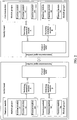
- the first example provided in the present invention is a method for switching the active and standby boards, and the composition units of the system for switching the active and standby using this method is shown in FIG. 2 .
- FIG. 2 As a whole system, two boards of the active board and the standby board are comprised, and they have the completely same internal structure, and the following will take one board thereinto as an example to describe the composition modules.
- a control module MSC is composed of a hardware unit, and its function is to respond to the switching triggering signal and complete the pre-switching processing, and said pre-switching processing is for pre-judging whether the switching condition is satisfied, and providing a control signal after the initial processing to the execution module of the latter stage;
- a switching execution module which is composed of the software unit and the hardware unit together, comprises 2 sub-modules, namely a switching execution module A which controls the switching of the function modules being unable to be in the active state at the same time and a switching execution module B which controls the switching of the function modules being unable to be in the standby state at the same time.
- Function modules comprise a plurality of different function modules a1, a2, ... , am, b1, b2, ... , bn, and in FIG. 2 , the function modules a1, a2, ... , am which are unable to be in the active state at the same time are classified as one type of module group a; the function modules b1, b2, ... , bn which are unable to be in the standby state at the same time are classified as one type of module group b; and in the practical application, the simplest example can only have a1 and b1.
- the interconnection signal interfaces between the active and standby boards are generally divided into two groups of input interconnection signal interfaces and output interconnection signal interfaces, which provide connections for the control modules MSC of the active board and the standby board.
- the module group a and module group b on the active board are in the active state and the module group a and module group b on the standby board are in the standby state before carrying out the active and standby switching, and the module group a and module group b on the active board are in the standby state and the module group a and module group b on the standby board are in the active state after switching, and the particular switching process comprises following steps:
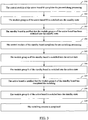
- the flow of the method according to this example is as shown in FIG. 3 , and comprises:
- the switching is triggered before step 101: when a certain external or internal triggering condition changes, the switching process is triggered, and the triggering message is transmitted to the control module at first, and it is the control module of the active board M that starts the switching operation at first. Certainly, it also can be the control module of the standby board that starts the switching operation at first.
- the switching shielding function can be started so as to ensure not to respond to the new switching request any more before not completing the switching process completely.
- Step 102 under the processing of the switching execution module A, the active board M will complete the switching of the function modules which are unable to be in the active state at the same time, and switch a1, a2, ... , am into the standby state in sequence or at the same time, and generates a next stage control signal to send to the control module after all the function modules of the a1 ⁇ am complete the state switching.
- Step 103 the control module will send the information sent by the switching execution module A to the control module of the standby board S through the interconnection signal interface between the active and standby boards, and the module group a of the active board has been switched into the standby state.
- Step 104 the control module of the standby board S will complete the pre-switching processing, and generates the secondary stage control signal to notify the switching execution module A of the standby board.
- Step 105 under the control of the switching execution module A of the standby board S, a1, a2, ... , am function modules of the standby board S are switched into the active state in sequence, and a next stage control signal is generated to be sent to the control module after all of these function modules complete the state switching.
- these units of the two boards are in the standby state at the same time in the duration from the time after the a1, a2, ... , am of the active board M are switched into the standby state to the time of the a1, A2,... , am of the standby board S being switched into the active state.
- Step 106 the control module will send a message to notify the switching execution module B after receiving that the a1, a2, ... , am have been switched into the standby state.
- the switching execution module B will be responsible for switching the b1, b2, ... , bn function modules of the standby board into the active state in sequence or at the same time. And a next stage control signal is generated to notify the control module after all of these function modules are switched into the active state.
- Step 107 the control module of the standby board S will notify the control module of the board on the other end (the active board M) through the interconnection signal interface between the boards after receiving the message that the b1, b2, ... , bn have been switched into the active state. So far, all the function modules of the standby board S have initially completed the state switching, and are stabilized in the active state.
- Step 108 the control module of the active board M will notify the switching execution module B to execute the switching.
- the switching execution module B is responsible for switching b1, b2, ... , bn function modules into the standby state in sequence, and generating a next stage control signal to return to the pre-switching control module after all of these function modules completes the state switching.
- these units of the two boards are in the active state at the same time in the duration from the time after the b1, b2, ... , bn of the standby board S are switched into the active state to the time of the b1, b2, ... , bn of the active board M being switched into the standby state.
- Step 109 the control module of the active board M judges that the switching process is completed according to the returned signal, and stabilizes all the states, and if the switching shielding mechanism is started, then it should recover to the normal state.
- the abnormal case occurring in the switching process can be processed as the following way: when the switching is executed in the mid process, it is detected that the current state is unable to continue the switching, and the state before the switching is recovered in a way of performing in a strict inverse order.
- a plurality of function modules c1, c2,... , cx are further comprised, they do not have the requirement for the active and standby states, for example, the function modules c1, c2, ..., cx can be in the active state or the standby state at the same time in the active board and the standby board, or be in the active state in the active board and be in the standby state in the standby board, and also can be in the standby state in the active board and be in the active state in the standby board.
- the processing according to the way of the switching execution module A the other is the processing according to the way of the switching execution module B.
- the active and standby states of the c1, c2, ..., cx can be switched just after completing the switching of the a1, a2, ... , am in steps 102 and 105.
- the active and standby states of the c1, c2, ..., cx can be switched just after completing the switching of the b1, b2, ... , bn in steps 106 and 108.
- the suitable range of this scheme includes the simplest system comprising two modules, and even the complex system comprising a plurality of modules, and all of these can be ensured to securely implement the active and standby switching. As long as these modules are divided into the module group of avoiding both being in the active state and the module group of avoiding both being in the standby state according to the different function requirements, the switching can be implemented securely stage by stage according to the method described in this scheme.
- the present invention provides the second example, and the flow of the method is shown in FIG. 4 , and comprises:
- the third example provided in the present invention is an apparatus for switching an active board and a standby board, and as shown in FIG. 5 , this apparatus comprises:
- the first switching execution module 301 is used for switching the first type function module on the first working state board into the second working state, said first type function module being unable to be in the first working state on the first working state board and the second working state board at the same time, and switching the first type function module on the second working state board into the first working state, and said first working state is the active state and the second working state is the standby state, or said second working state is the active state and the first working state is the standby state;
- the second switching execution module 302 is used for switching the second type function module on the second working state board into the first working state, said second type function module being unable to be in the second working state on the first working state board and the second working state board at the same time, and switching the second type function module on the first working state board into the second working state.
- said apparatus further comprises:
- the first switching execution module 301 is further used for switching the first type function module on the first working state board into the second working state according to the first switching notification, and switching the first type function module on the second working state board into the first working state according to the first switching notification;
- the second switching execution module 302 is further used for switching the second type function module on the second working state board into the first working state according to the second switching notification, and switching the second type function module on the first working state board into the second working state according to the second switching notification.
- control module 303 is used for carrying out the switching shielding to forbid responding to the new switching request after determining that the first working state board is able to be switched; and is further used for relieving the switching shielding after completing all the switchings.
- the first switching execution module 301 is further used for switching the third type function module on the first working state board into the second working state, switching the third type function module on the second working state board into the first working state, and said third type function module is in the first working state or the second working state on the first working state board and the second working state board at the same time, or said third type function module is in the first working state on the first working state board, and is in the second working state on the second working state board, or said third type function module is in the second working state on the first working state board, and is in the first working state on the second working state board;
- the second switching execution module 302 is further used for switching the third type function module on the second working state board into the first working state, and switching the third type function module on the first working state board into the second working state.
- the method and apparatus for switching an active board and a standby board provided in the present invention switch function modules according to different types in sequence, so as to implement the active and standby switching in the system comprising a plurality of function units which are required to avoid being in the active state at the same time and a plurality of function units which are required to avoid being in the standby state at the same time.
Landscapes
- Engineering & Computer Science (AREA)
- Computer Networks & Wireless Communication (AREA)
- Signal Processing (AREA)
- Data Exchanges In Wide-Area Networks (AREA)
- Hardware Redundancy (AREA)
Claims (13)
- Verfahren zum Schalten einer aktiven Leiterplatte und einer Bereitschaftsleiterplatte, umfassend, dass:ein Funktionsmodul vom ersten Typ an einer Leiterplatte im ersten Arbeitszustand von einem ersten Arbeitszustand in einen zweiten Arbeitszustand geschaltet (102, 206) wird, wobei das Funktionsmodul vom ersten Typ nicht in der Lage ist, sich gleichzeitig in dem ersten Arbeitszustand an der Leiterplatte im ersten Arbeitszustand und an der Leiterplatte im zweiten Arbeitszustand zu befinden, und dann das Funktionsmodul vom ersten Typ an der Leiterplatte im zweiten Arbeitszustand von dem zweiten Arbeitszustand in den ersten Arbeitszustand geschaltet (105, 208) wird;ein Funktionsmodul vom zweiten Typ an der Leiterplatte im zweiten Arbeitszustand von dem zweiten Arbeitszustand in den ersten Arbeitszustand geschaltet (106, 202) wird, wobei das Funktionsmodul vom zweiten Typ nicht in der Lage ist, gleichzeitig in dem zweiten Arbeitszustand an der Leiterplatte im ersten Arbeitszustand und der Leiterplatte im zweiten Arbeitszustand zu sein, und dann das Funktionsmodul vom zweiten Typ an der Leiterplatte im ersten Arbeitszustand von dem ersten Arbeitszustand in den zweiten Arbeitszustand geschaltet (108, 205) wird;wobei die Leiterplatte im ersten Arbeitszustand eine von der aktiven Leiterplatte und der Bereitschaftsleiterplatte ist, und die Leiterplatte im zweiten Arbeitszustand die andere der aktiven Leiterplatte und der Bereitschaftsleiterplatte ist;wobei, wenn die Leiterplatte im ersten Arbeitszustand die aktive Leiterplatte ist und die Leiterplatte im zweiten Arbeitszustand die Bereitschaftsleiterplatte ist, der erste Arbeitszustand ein aktiver Zustand ist und der zweite Arbeitszustand ein Bereitschaftszustand ist; und wobei, wenn die Leiterplatte im ersten Arbeitszustand die Bereitschaftsleiterplatte ist und die Leiterplatte im zweiten Arbeitszustand die aktive Leiterplatte ist, der erste Arbeitszustand der Bereitschafszustand ist und der zweite Arbeitszustand der aktive Zustand ist.
- Verfahren nach Anspruch 1, wobei vor dem Schritt zum Schalten (102, 206) des Funktionsmoduls vom ersten Typ an der Leiterplatte im ersten Arbeitszustand von dem ersten Arbeitszustand in den zweiten Arbeitszustand ferner umfasst ist, dass bestimmt wird, dass die Leiterplatte im ersten Arbeitszustand geschaltet werden kann, und eine erste Schaltbenachrichtigung gesendet wird.
- Verfahren nach Anspruch 2, wobeider Schritt zum Schalten (102, 206) des Funktionsmoduls vom ersten Typ an der Leiterplatte im ersten Arbeitszustand von dem ersten Arbeitszustand in den zweiten Arbeitszustand umfasst, dass das Funktionsmodul vom ersten Typ an der Leiterplatte im ersten Arbeitszustand von dem ersten Arbeitszustand in den zweiten Arbeitszustand gemäß der ersten Schaltbenachrichtigung geschaltet wird;der Schritt zum Schalten (105, 208) des Funktionsmoduls vom ersten Typ an der Leiterplatte im zweiten Arbeitszustand von dem zweiten Arbeitszustand in den ersten Arbeitszustand umfasst, dass das Funktionsmodul vom ersten Typ an der Leiterplatte im zweiten Arbeitszustand von dem zweiten Arbeitszustand in den ersten Arbeitszustand gemäß der ersten Schaltbenachrichtigung geschaltet wird.
- Verfahren nach Anspruch 1, wobei vor dem Schritt zum Schalten (106, 202) des Funktionsmoduls vom zweiten Typ an der Leiterplatte im zweiten Arbeitszustand von dem zweiten Arbeitszustand in den ersten Arbeitszustand ferner umfasst ist, dass bestimmt wird, dass die Leiterplatte im zweiten Arbeitszustand geschaltet werden kann, und dass eine zweite Schaltbenachrichtigung gesendet wird.
- Verfahren nach Anspruch 4, wobeider Schritt zum Schalten (106, 202) des Funktionsmoduls vom zweiten Typ an der Leiterplatte im zweiten Arbeitszustand von dem zweiten Arbeitszustand in den ersten Arbeitszustand umfasst, dass das Funktionsmodul vom zweiten Typ an der Leiterplatte im zweiten Arbeitszustand von dem zweiten Arbeitszustand in den ersten Arbeitszustand gemäß der zweiten Schaltbenachrichtigung geschaltet wird;der Schritt (108, 205) zum Schalten des Funktionsmoduls vom zweiten Typ an der Leiterplatte im ersten Arbeitszustand von dem ersten Arbeitszustand in den zweiten Arbeitszustand umfasst, dass das Funktionsmodul vom zweiten Typ an der Leiterplatte im ersten Arbeitszustand von dem ersten Arbeitszustand in den zweiten Arbeitszustand gemäß der zweiten Schaltbenachrichtigung geschaltet wird.
- Verfahren nach Anspruch 2, ferner umfassend, dass eine Schaltabschirmung ausgeführt wird, um ein Reagieren auf eine neue Schaltanforderung zu verbieten, nachdem bestimmt worden ist, dass die Leiterplatte im ersten Arbeitszustand geschaltet werden kann.
- Verfahren nach Anspruch 1, wobeinach dem Schritt zum Schalten des Funktionsmoduls vom ersten Typ an der Leiterplatte im ersten Arbeitszustand von dem ersten Arbeitszustand in den zweiten Arbeitszustand und dem Schalten des Funktionsmoduls vom ersten Typ an der Leiterplatte im zweiten Arbeitszustand von dem zweiten Arbeitszustand in den ersten Arbeitszustand ferner umfasst ist, dass:ein Funktionsmodul vom dritten Typ an der Leiterplatte im ersten Arbeitszustand von dem ersten Arbeitszustand in den zweiten Arbeitszustand geschaltet wird und das Funktionsmodul vom dritten Typ an der Leiterplatte im zweiten Arbeitszustand von dem zweiten Arbeitszustand in den ersten Arbeitszustand geschaltet wird, wobei das Funktionsmodul vom dritten Typ gleichzeitig in dem ersten Arbeitszustand und dem zweiten Arbeitszustand an der Leiterplatte des ersten Arbeitszustandes oder der Leiterplatte im zweiten Arbeitszustand ist oder das Funktionsmodul vom dritten Typ in dem ersten Arbeitszustand an der Leiterplatte im ersten Arbeitszustand ist und in dem zweiten Arbeitszustand an der Leiterplatte im zweiten Arbeitszustand ist, oder das Funktionsmodul vom dritten Typ in dem zweiten Arbeitszustand an der Leiterplatte im ersten Arbeitszustand ist und in dem ersten Arbeitszustand an der Leiterplatte im zweiten Arbeitszustand ist;nach dem Schritt zum Schalten des Funktionsmoduls vom zweiten Typ an der Leiterplatte im zweiten Arbeitszustand von dem zweiten Arbeitszustand in den ersten Arbeitszustand und dem Schalten des Funktionsmoduls vom zweiten Typ an der Leiterplatte im ersten Arbeitszustand von dem ersten Arbeitszustand in den zweiten Arbeitszustand ferner umfasst ist, dass:das Funktionsmodul vom dritten Typ an der Leiterplatte im zweiten Arbeitszustand von dem zweiten Arbeitszustand in den ersten Arbeitszustand geschaltet wird und das Funktionsmodul vom dritten Typ an der Leiterplatte im ersten Arbeitszustand von dem ersten Arbeitszustand in den zweiten Arbeitszustand geschaltet wird.
- Verfahren nach Anspruch 6, ferner umfassend, dass die Schaltabschirmung freigegeben wird, nachdem alle Schaltvorgänge beendet sind.
- Vorrichtung zum Schalten einer aktiven Leiterplatte und einer Bereitschaftsleiterplatte, umfassend:ein erstes Schaltausführmodul (301), das so konfiguriert ist, ein Funktionsmodul vom ersten Typ an der Leiterplatte im ersten Arbeitszustand von einem ersten Arbeitszustand in einen zweiten Arbeitszustand zu schalten, wobei das Funktionsmodul vom ersten Typ nicht in der Lage ist, sich gleichzeitig in dem ersten Arbeitszustand an der Leiterplatte im ersten Arbeitszustand und der Leiterplatte im zweiten Arbeitszustand zu befinden, und das Funktionsmodul vom ersten Typ an der Leiterplatte im zweiten Arbeitszustand von dem zweiten Arbeitszustand in den ersten Arbeitszustand zu schalten; undein zweites Schaltausführmodul (302), das so konfiguriert ist, ein Funktionsmodul vom zweiten Typ an der Leiterplatte im zweiten Arbeitszustand von dem zweiten Arbeitszustand in den ersten Arbeitszustand zu schalten, wobei das Funktionsmodul vom zweiten Typ nicht in der Lage ist, sich gleichzeitig in dem zweiten Arbeitszustand an der Leiterplatte im ersten Arbeitszustand und der Leiterplatte im zweiten Arbeitszustand zu befinden und das Funktionsmodul vom zweiten Typ an der Leiterplatte im ersten Arbeitszustand von dem ersten Arbeitszustand in den zweiten Arbeitszustand zu schalten;wobei die Leiterplatte im ersten Arbeitszustand eine der aktiven Leiterplatte und der Bereitschaftsplatte ist, und die Leiterplatte im zweiten Arbeitszustand die andere der aktiven Leiterplatte und der Bereitschaftsplatte ist;wobei, wenn die Leiterplatte im ersten Arbeitszustand die aktive Leiterplatte ist und die Leiterplatte im zweiten Arbeitszustand die Bereitschaftsleiterplatte ist, der erste Arbeitszustand ein aktiver Zustand ist und der zweite Arbeitszustand ein Bereitschaftszustand ist; und wobei, wenn die Leiterplatte im ersten Arbeitszustand die Bereitschaftsplatte ist und die Leiterplatte im zweiten Arbeitszustand die aktive Platte ist, der erste Arbeitszustand der Bereitschaftszustand ist und der zweite Arbeitszustand der aktive Zustand ist.
- Vorrichtung nach Anspruch 9, ferner umfassend:ein Steuermodul (303), das so konfiguriert ist, um zu bestimmen, dass die Leiterplatte im ersten Arbeitszustand geschaltet werden kann, und eine erste Schaltbenachrichtigung zu senden, und zu bestimmen, dass die Leiterplatte im zweiten Arbeitszustand geschaltet werden kann, und eine zweite Schaltbenachrichtigung zu senden.
- Vorrichtung nach Anspruch 10, wobeidas erste Schaltausführmodul (301) ferner derart konfiguriert ist, das Funktionsmodul vom ersten Typ an der Leiterplatte im ersten Arbeitszustand von dem ersten Arbeitszustand in den zweiten Arbeitszustand gemäß der ersten Schaltbenachrichtigung zu schalten und das Funktionsmodul vom ersten Typ an der Leiterplatte im zweiten Arbeitszustand von dem zweiten Arbeitszustand in den ersten Arbeitszustand gemäß der ersten Schaltbenachrichtigung zu schalten;wobei das zweite Schaltausführmodul (302) ferner derart konfiguriert ist, das Funktionsmodul vom zweiten Typ an der Leiterplatte im zweiten Arbeitszustand von dem zweiten Arbeitszustand in den ersten Arbeitszustand gemäß der zweiten Schaltbenachrichtigung zu schalten und das Funktionsmodul vom zweiten Typ an der Leiterplatte im ersten Arbeitszustand von dem ersten Arbeitszustand in den zweiten Arbeitszustand gemäß der zweiten Schaltbenachrichtigung zu schalten.
- Vorrichtung nach Anspruch 10, wobei das Steuermodul (303) ferner derart konfiguriert ist, eine Schaltabschirmung auszuführen, um das Reagieren auf eine neue Schaltanforderung zu verbieten, nachdem bestimmt worden ist, dass die Leiterplatte im ersten Arbeitszustand geschaltet werden kann; und ferner derart konfiguriert ist, die Schaltabschirmung freizugeben, nachdem alle Schaltvorgänge beendet sind.
- Vorrichtung nach Anspruch 9, wobeidas erste Schaltausführmodul (301) ferner derart konfiguriert ist, ein Funktionsmodul vom dritten Typ an der Leiterplatte im ersten Arbeitszustand von dem ersten Arbeitszustand in den zweiten Arbeitszustand zu schalten und das Funktionsmodul vom dritten Typ an der Leiterplatte im zweiten Arbeitszustand von dem zweiten Arbeitszustand in den ersten Arbeitszustand zu schalten, wobei das Funktionsmodul vom dritten Typ sich gleichzeitig in dem ersten Arbeitszustand oder dem zweiten Arbeitszustand an der Leiterplatte im ersten Arbeitszustand und der Leiterplatte im zweiten Arbeitszustand befindet oder sich das Funktionsmodul vom dritten Typ in dem ersten Arbeitszustand an der Leiterplatte im ersten Arbeitszustand befindet und sich in dem zweiten Arbeitszustand an der Leiterplatte im zweiten Arbeitszustand befindet, oder dass das Funktionsmodul vom dritten Typ sich in dem zweiten Arbeitszustand an der Leiterplatte im ersten Arbeitszustand befindet und sich in dem ersten Arbeitszustand an der Leiterplatte im zweiten Arbeitszustand befindet;wobei das zweite Schaltausführmodul (302) ferner derart konfiguriert ist, das Funktionsmodul vom dritten Typ an der Leiterplatte im zweiten Arbeitszustand von dem zweiten Arbeitszustand in den ersten Arbeitszustand zu schalten und das Funktionsmodul vom dritten Typ an der Leiterplatte im ersten Arbeitszustand von dem ersten Arbeitszustand in den zweiten Arbeitszustand zu schalten.
Applications Claiming Priority (2)
| Application Number | Priority Date | Filing Date | Title |
|---|---|---|---|
| CN2009102032326A CN101562513B (zh) | 2009-05-25 | 2009-05-25 | 一种单板主备倒换的方法及装置 |
| PCT/CN2009/073918 WO2010135882A1 (zh) | 2009-05-25 | 2009-09-14 | 一种倒换主备单板的方法及装置 |
Publications (3)
| Publication Number | Publication Date |
|---|---|
| EP2432152A1 EP2432152A1 (de) | 2012-03-21 |
| EP2432152A4 EP2432152A4 (de) | 2014-08-06 |
| EP2432152B1 true EP2432152B1 (de) | 2017-03-15 |
Family
ID=41221146
Family Applications (1)
| Application Number | Title | Priority Date | Filing Date |
|---|---|---|---|
| EP09845098.4A Not-in-force EP2432152B1 (de) | 2009-05-25 | 2009-09-14 | Verfahren und vorrichtung zur umschaltung einer haupt-/standby-einzelplatine |
Country Status (6)
| Country | Link |
|---|---|
| US (1) | US8762597B2 (de) |
| EP (1) | EP2432152B1 (de) |
| CN (1) | CN101562513B (de) |
| AU (1) | AU2009346823A1 (de) |
| ES (1) | ES2628226T3 (de) |
| WO (1) | WO2010135882A1 (de) |
Families Citing this family (1)
| Publication number | Priority date | Publication date | Assignee | Title |
|---|---|---|---|---|
| CN101777996B (zh) * | 2009-12-29 | 2013-04-10 | 中兴通讯股份有限公司 | 一种实现业务主备切换的装置及方法 |
Family Cites Families (12)
| Publication number | Priority date | Publication date | Assignee | Title |
|---|---|---|---|---|
| JPH11225129A (ja) * | 1998-02-06 | 1999-08-17 | Hitachi Ltd | 自動回線切替システム |
| US6091731A (en) * | 1998-03-30 | 2000-07-18 | Lucent Technologies Inc. | Duplication in asychronous transfer mode (ATM) network fabrics |
| JP2000330815A (ja) * | 1999-05-24 | 2000-11-30 | Matsushita Electric Ind Co Ltd | 二重化切替制御装置及び方法 |
| CN1109416C (zh) * | 2000-04-25 | 2003-05-21 | 华为技术有限公司 | 交换机的主备倒换方法及其实现装置 |
| CN1156995C (zh) * | 2000-07-11 | 2004-07-07 | 深圳市中兴通讯股份有限公司 | 数字通讯系统中可热插拔主备无抖动切换方法及装置 |
| CN1248425C (zh) * | 2002-02-07 | 2006-03-29 | 华为技术有限公司 | 一种通讯设备中的主备倒换方法 |
| CN1299438C (zh) * | 2002-11-02 | 2007-02-07 | 华为技术有限公司 | 一种实现单板主备倒换的方法及其电路 |
| US7577090B2 (en) * | 2004-02-13 | 2009-08-18 | Alcatel-Lucent Usa Inc. | Method and system for providing availability and reliability for a telecommunication network entity |
| CN100362761C (zh) * | 2004-09-28 | 2008-01-16 | 华为技术有限公司 | 一种实现单板倒换的方法 |
| CN100440799C (zh) * | 2005-09-06 | 2008-12-03 | 华为技术有限公司 | 一种接入设备中主备板备份及倒换的方法 |
| CN101110609A (zh) * | 2007-08-23 | 2008-01-23 | 华为技术有限公司 | 主、备用模块实现通信的方法和系统 |
| US7808982B2 (en) * | 2008-06-03 | 2010-10-05 | Hewlett-Packard Development Company, L.P. | Method for verifying shared state synchronization of redundant modules in a high availability network switch |
-
2009
- 2009-05-25 CN CN2009102032326A patent/CN101562513B/zh not_active Expired - Fee Related
- 2009-09-14 WO PCT/CN2009/073918 patent/WO2010135882A1/zh not_active Ceased
- 2009-09-14 AU AU2009346823A patent/AU2009346823A1/en not_active Abandoned
- 2009-09-14 EP EP09845098.4A patent/EP2432152B1/de not_active Not-in-force
- 2009-09-14 US US13/258,442 patent/US8762597B2/en not_active Expired - Fee Related
- 2009-09-14 ES ES09845098.4T patent/ES2628226T3/es active Active
Non-Patent Citations (1)
| Title |
|---|
| None * |
Also Published As
| Publication number | Publication date |
|---|---|
| CN101562513B (zh) | 2012-02-29 |
| US20120056489A1 (en) | 2012-03-08 |
| WO2010135882A1 (zh) | 2010-12-02 |
| EP2432152A4 (de) | 2014-08-06 |
| US8762597B2 (en) | 2014-06-24 |
| ES2628226T3 (es) | 2017-08-02 |
| AU2009346823A1 (en) | 2012-01-19 |
| CN101562513A (zh) | 2009-10-21 |
| EP2432152A1 (de) | 2012-03-21 |
Similar Documents
| Publication | Publication Date | Title |
|---|---|---|
| KR101298558B1 (ko) | 메인/예비 보드의 스위칭 방법 및 시스템 | |
| EP4084492A1 (de) | Verfahren, system und olt zum schutz von pon mit doppelter elternschaft | |
| CN103152419A (zh) | 一种云计算平台的高可用集群管理方法 | |
| EP2466800A2 (de) | Elektronische patch-vorrichtung, netzwerksystem und betriebsverfahren in einem netzwerksystem | |
| EP3442163B1 (de) | Datenverarbeitungssystem mit dienstkontinuitätsschutz | |
| EP2224341A1 (de) | Knotensystem, serverumschaltungsverfahren, servergerät und datenübertragungsverfahren | |
| CN103856357A (zh) | 一种堆叠系统故障处理方法及堆叠系统 | |
| CN103702065A (zh) | 一种视频会议系统的备份系统及方法 | |
| CN105656711A (zh) | 信号检测方法及装置 | |
| CN106095571B (zh) | 多rac集群系统、数据访问方法及装置 | |
| CN102571458A (zh) | 隧道保护组的切换方法及装置 | |
| CN105790965A (zh) | 链路切换方法、装置及线卡 | |
| EP2445118B1 (de) | Verfahren und vorrichtung zum schutz von auf automatisch geschalteten optischen netzwerken beruhenden diensten | |
| US8762597B2 (en) | Method and apparatus for switching the main/standby single board | |
| CN111045863A (zh) | 一种传感器数据分配网络故障容错架构及方法 | |
| CN111698157B (zh) | 一种链路管理方法、板卡及交换机 | |
| CN114095462A (zh) | 一种雷达处理机srio通信系统的容错方法及系统 | |
| CN103001810B (zh) | 网络业务通道保护切换方法及系统 | |
| JP2010231257A (ja) | 高可用性システム、高可用性システムの対障害対策方法 | |
| CN103716186B (zh) | 具有网络故障容错能力的人工话务系统及其方法 | |
| CN103744755A (zh) | 主备单板端口共享保护的实现系统及方法 | |
| JP6411790B2 (ja) | 通信システムおよび通信方法 | |
| US12155559B2 (en) | Communication control device, communication control method, communication control program, and communication control system | |
| US8248914B2 (en) | Gateway device and method for maintaining a communication connection therethrough | |
| CN101686118B (zh) | 一种交换业务系统及其工作方法 |
Legal Events
| Date | Code | Title | Description |
|---|---|---|---|
| PUAI | Public reference made under article 153(3) epc to a published international application that has entered the european phase |
Free format text: ORIGINAL CODE: 0009012 |
|
| 17P | Request for examination filed |
Effective date: 20111214 |
|
| AK | Designated contracting states |
Kind code of ref document: A1 Designated state(s): AT BE BG CH CY CZ DE DK EE ES FI FR GB GR HR HU IE IS IT LI LT LU LV MC MK MT NL NO PL PT RO SE SI SK SM TR |
|
| DAX | Request for extension of the european patent (deleted) | ||
| REG | Reference to a national code |
Ref country code: DE Ref legal event code: R079 Ref document number: 602009044852 Country of ref document: DE Free format text: PREVIOUS MAIN CLASS: H04L0001240000 Ipc: H04L0001220000 |
|
| A4 | Supplementary search report drawn up and despatched |
Effective date: 20140703 |
|
| RIC1 | Information provided on ipc code assigned before grant |
Ipc: H04L 1/22 20060101AFI20140629BHEP |
|
| GRAP | Despatch of communication of intention to grant a patent |
Free format text: ORIGINAL CODE: EPIDOSNIGR1 |
|
| INTG | Intention to grant announced |
Effective date: 20161011 |
|
| GRAS | Grant fee paid |
Free format text: ORIGINAL CODE: EPIDOSNIGR3 |
|
| STAA | Information on the status of an ep patent application or granted ep patent |
Free format text: STATUS: GRANT OF PATENT IS INTENDED |
|
| GRAA | (expected) grant |
Free format text: ORIGINAL CODE: 0009210 |
|
| STAA | Information on the status of an ep patent application or granted ep patent |
Free format text: STATUS: THE PATENT HAS BEEN GRANTED |
|
| AK | Designated contracting states |
Kind code of ref document: B1 Designated state(s): AT BE BG CH CY CZ DE DK EE ES FI FR GB GR HR HU IE IS IT LI LT LU LV MC MK MT NL NO PL PT RO SE SI SK SM TR |
|
| REG | Reference to a national code |
Ref country code: CH Ref legal event code: EP Ref country code: GB Ref legal event code: FG4D |
|
| REG | Reference to a national code |
Ref country code: IE Ref legal event code: FG4D |
|
| REG | Reference to a national code |
Ref country code: AT Ref legal event code: REF Ref document number: 876550 Country of ref document: AT Kind code of ref document: T Effective date: 20170415 |
|
| REG | Reference to a national code |
Ref country code: DE Ref legal event code: R096 Ref document number: 602009044852 Country of ref document: DE |
|
| REG | Reference to a national code |
Ref country code: NL Ref legal event code: MP Effective date: 20170315 |
|
| REG | Reference to a national code |
Ref country code: LT Ref legal event code: MG4D |
|
| PG25 | Lapsed in a contracting state [announced via postgrant information from national office to epo] |
Ref country code: HR Free format text: LAPSE BECAUSE OF FAILURE TO SUBMIT A TRANSLATION OF THE DESCRIPTION OR TO PAY THE FEE WITHIN THE PRESCRIBED TIME-LIMIT Effective date: 20170315 Ref country code: NO Free format text: LAPSE BECAUSE OF FAILURE TO SUBMIT A TRANSLATION OF THE DESCRIPTION OR TO PAY THE FEE WITHIN THE PRESCRIBED TIME-LIMIT Effective date: 20170615 Ref country code: FI Free format text: LAPSE BECAUSE OF FAILURE TO SUBMIT A TRANSLATION OF THE DESCRIPTION OR TO PAY THE FEE WITHIN THE PRESCRIBED TIME-LIMIT Effective date: 20170315 Ref country code: GR Free format text: LAPSE BECAUSE OF FAILURE TO SUBMIT A TRANSLATION OF THE DESCRIPTION OR TO PAY THE FEE WITHIN THE PRESCRIBED TIME-LIMIT Effective date: 20170616 Ref country code: LT Free format text: LAPSE BECAUSE OF FAILURE TO SUBMIT A TRANSLATION OF THE DESCRIPTION OR TO PAY THE FEE WITHIN THE PRESCRIBED TIME-LIMIT Effective date: 20170315 |
|
| REG | Reference to a national code |
Ref country code: ES Ref legal event code: FG2A Ref document number: 2628226 Country of ref document: ES Kind code of ref document: T3 Effective date: 20170802 |
|
| REG | Reference to a national code |
Ref country code: AT Ref legal event code: MK05 Ref document number: 876550 Country of ref document: AT Kind code of ref document: T Effective date: 20170315 |
|
| PG25 | Lapsed in a contracting state [announced via postgrant information from national office to epo] |
Ref country code: BG Free format text: LAPSE BECAUSE OF FAILURE TO SUBMIT A TRANSLATION OF THE DESCRIPTION OR TO PAY THE FEE WITHIN THE PRESCRIBED TIME-LIMIT Effective date: 20170615 Ref country code: SE Free format text: LAPSE BECAUSE OF FAILURE TO SUBMIT A TRANSLATION OF THE DESCRIPTION OR TO PAY THE FEE WITHIN THE PRESCRIBED TIME-LIMIT Effective date: 20170315 Ref country code: LV Free format text: LAPSE BECAUSE OF FAILURE TO SUBMIT A TRANSLATION OF THE DESCRIPTION OR TO PAY THE FEE WITHIN THE PRESCRIBED TIME-LIMIT Effective date: 20170315 |
|
| PG25 | Lapsed in a contracting state [announced via postgrant information from national office to epo] |
Ref country code: NL Free format text: LAPSE BECAUSE OF FAILURE TO SUBMIT A TRANSLATION OF THE DESCRIPTION OR TO PAY THE FEE WITHIN THE PRESCRIBED TIME-LIMIT Effective date: 20170315 |
|
| REG | Reference to a national code |
Ref country code: FR Ref legal event code: PLFP Year of fee payment: 9 |
|
| PG25 | Lapsed in a contracting state [announced via postgrant information from national office to epo] |
Ref country code: IT Free format text: LAPSE BECAUSE OF FAILURE TO SUBMIT A TRANSLATION OF THE DESCRIPTION OR TO PAY THE FEE WITHIN THE PRESCRIBED TIME-LIMIT Effective date: 20170315 Ref country code: CZ Free format text: LAPSE BECAUSE OF FAILURE TO SUBMIT A TRANSLATION OF THE DESCRIPTION OR TO PAY THE FEE WITHIN THE PRESCRIBED TIME-LIMIT Effective date: 20170315 Ref country code: RO Free format text: LAPSE BECAUSE OF FAILURE TO SUBMIT A TRANSLATION OF THE DESCRIPTION OR TO PAY THE FEE WITHIN THE PRESCRIBED TIME-LIMIT Effective date: 20170315 Ref country code: SK Free format text: LAPSE BECAUSE OF FAILURE TO SUBMIT A TRANSLATION OF THE DESCRIPTION OR TO PAY THE FEE WITHIN THE PRESCRIBED TIME-LIMIT Effective date: 20170315 Ref country code: AT Free format text: LAPSE BECAUSE OF FAILURE TO SUBMIT A TRANSLATION OF THE DESCRIPTION OR TO PAY THE FEE WITHIN THE PRESCRIBED TIME-LIMIT Effective date: 20170315 Ref country code: EE Free format text: LAPSE BECAUSE OF FAILURE TO SUBMIT A TRANSLATION OF THE DESCRIPTION OR TO PAY THE FEE WITHIN THE PRESCRIBED TIME-LIMIT Effective date: 20170315 |
|
| PG25 | Lapsed in a contracting state [announced via postgrant information from national office to epo] |
Ref country code: PL Free format text: LAPSE BECAUSE OF FAILURE TO SUBMIT A TRANSLATION OF THE DESCRIPTION OR TO PAY THE FEE WITHIN THE PRESCRIBED TIME-LIMIT Effective date: 20170315 Ref country code: PT Free format text: LAPSE BECAUSE OF FAILURE TO SUBMIT A TRANSLATION OF THE DESCRIPTION OR TO PAY THE FEE WITHIN THE PRESCRIBED TIME-LIMIT Effective date: 20170717 Ref country code: IS Free format text: LAPSE BECAUSE OF FAILURE TO SUBMIT A TRANSLATION OF THE DESCRIPTION OR TO PAY THE FEE WITHIN THE PRESCRIBED TIME-LIMIT Effective date: 20170715 Ref country code: SM Free format text: LAPSE BECAUSE OF FAILURE TO SUBMIT A TRANSLATION OF THE DESCRIPTION OR TO PAY THE FEE WITHIN THE PRESCRIBED TIME-LIMIT Effective date: 20170315 |
|
| REG | Reference to a national code |
Ref country code: DE Ref legal event code: R097 Ref document number: 602009044852 Country of ref document: DE |
|
| PLBE | No opposition filed within time limit |
Free format text: ORIGINAL CODE: 0009261 |
|
| STAA | Information on the status of an ep patent application or granted ep patent |
Free format text: STATUS: NO OPPOSITION FILED WITHIN TIME LIMIT |
|
| PG25 | Lapsed in a contracting state [announced via postgrant information from national office to epo] |
Ref country code: DK Free format text: LAPSE BECAUSE OF FAILURE TO SUBMIT A TRANSLATION OF THE DESCRIPTION OR TO PAY THE FEE WITHIN THE PRESCRIBED TIME-LIMIT Effective date: 20170315 |
|
| 26N | No opposition filed |
Effective date: 20171218 |
|
| PG25 | Lapsed in a contracting state [announced via postgrant information from national office to epo] |
Ref country code: SI Free format text: LAPSE BECAUSE OF FAILURE TO SUBMIT A TRANSLATION OF THE DESCRIPTION OR TO PAY THE FEE WITHIN THE PRESCRIBED TIME-LIMIT Effective date: 20170315 |
|
| REG | Reference to a national code |
Ref country code: CH Ref legal event code: PL |
|
| GBPC | Gb: european patent ceased through non-payment of renewal fee |
Effective date: 20170914 |
|
| PG25 | Lapsed in a contracting state [announced via postgrant information from national office to epo] |
Ref country code: MC Free format text: LAPSE BECAUSE OF FAILURE TO SUBMIT A TRANSLATION OF THE DESCRIPTION OR TO PAY THE FEE WITHIN THE PRESCRIBED TIME-LIMIT Effective date: 20170315 |
|
| REG | Reference to a national code |
Ref country code: IE Ref legal event code: MM4A |
|
| REG | Reference to a national code |
Ref country code: BE Ref legal event code: MM Effective date: 20170930 |
|
| PG25 | Lapsed in a contracting state [announced via postgrant information from national office to epo] |
Ref country code: LU Free format text: LAPSE BECAUSE OF NON-PAYMENT OF DUE FEES Effective date: 20170914 |
|
| PG25 | Lapsed in a contracting state [announced via postgrant information from national office to epo] |
Ref country code: CH Free format text: LAPSE BECAUSE OF NON-PAYMENT OF DUE FEES Effective date: 20170930 Ref country code: LI Free format text: LAPSE BECAUSE OF NON-PAYMENT OF DUE FEES Effective date: 20170930 Ref country code: IE Free format text: LAPSE BECAUSE OF NON-PAYMENT OF DUE FEES Effective date: 20170914 Ref country code: GB Free format text: LAPSE BECAUSE OF NON-PAYMENT OF DUE FEES Effective date: 20170914 |
|
| PG25 | Lapsed in a contracting state [announced via postgrant information from national office to epo] |
Ref country code: BE Free format text: LAPSE BECAUSE OF NON-PAYMENT OF DUE FEES Effective date: 20170930 |
|
| REG | Reference to a national code |
Ref country code: FR Ref legal event code: PLFP Year of fee payment: 10 |
|
| PG25 | Lapsed in a contracting state [announced via postgrant information from national office to epo] |
Ref country code: MT Free format text: LAPSE BECAUSE OF NON-PAYMENT OF DUE FEES Effective date: 20170914 |
|
| PG25 | Lapsed in a contracting state [announced via postgrant information from national office to epo] |
Ref country code: HU Free format text: LAPSE BECAUSE OF FAILURE TO SUBMIT A TRANSLATION OF THE DESCRIPTION OR TO PAY THE FEE WITHIN THE PRESCRIBED TIME-LIMIT; INVALID AB INITIO Effective date: 20090914 |
|
| PG25 | Lapsed in a contracting state [announced via postgrant information from national office to epo] |
Ref country code: CY Free format text: LAPSE BECAUSE OF NON-PAYMENT OF DUE FEES Effective date: 20170315 |
|
| PG25 | Lapsed in a contracting state [announced via postgrant information from national office to epo] |
Ref country code: MK Free format text: LAPSE BECAUSE OF FAILURE TO SUBMIT A TRANSLATION OF THE DESCRIPTION OR TO PAY THE FEE WITHIN THE PRESCRIBED TIME-LIMIT Effective date: 20170315 |
|
| PGFP | Annual fee paid to national office [announced via postgrant information from national office to epo] |
Ref country code: DE Payment date: 20191022 Year of fee payment: 11 |
|
| PGFP | Annual fee paid to national office [announced via postgrant information from national office to epo] |
Ref country code: ES Payment date: 20191029 Year of fee payment: 11 Ref country code: FR Payment date: 20191029 Year of fee payment: 11 |
|
| PG25 | Lapsed in a contracting state [announced via postgrant information from national office to epo] |
Ref country code: TR Free format text: LAPSE BECAUSE OF FAILURE TO SUBMIT A TRANSLATION OF THE DESCRIPTION OR TO PAY THE FEE WITHIN THE PRESCRIBED TIME-LIMIT Effective date: 20170315 |
|
| REG | Reference to a national code |
Ref country code: DE Ref legal event code: R119 Ref document number: 602009044852 Country of ref document: DE |
|
| PG25 | Lapsed in a contracting state [announced via postgrant information from national office to epo] |
Ref country code: FR Free format text: LAPSE BECAUSE OF NON-PAYMENT OF DUE FEES Effective date: 20200930 Ref country code: DE Free format text: LAPSE BECAUSE OF NON-PAYMENT OF DUE FEES Effective date: 20210401 |
|
| REG | Reference to a national code |
Ref country code: ES Ref legal event code: FD2A Effective date: 20220118 |
|
| PG25 | Lapsed in a contracting state [announced via postgrant information from national office to epo] |
Ref country code: ES Free format text: LAPSE BECAUSE OF NON-PAYMENT OF DUE FEES Effective date: 20200915 |