EP2432071A1 - Apparatus for improving transmission bandwidth - Google Patents
Apparatus for improving transmission bandwidth Download PDFInfo
- Publication number
- EP2432071A1 EP2432071A1 EP10838631A EP10838631A EP2432071A1 EP 2432071 A1 EP2432071 A1 EP 2432071A1 EP 10838631 A EP10838631 A EP 10838631A EP 10838631 A EP10838631 A EP 10838631A EP 2432071 A1 EP2432071 A1 EP 2432071A1
- Authority
- EP
- European Patent Office
- Prior art keywords
- transmission line
- signal transmission
- substrate
- capacitor
- disposed
- Prior art date
- Legal status (The legal status is an assumption and is not a legal conclusion. Google has not performed a legal analysis and makes no representation as to the accuracy of the status listed.)
- Ceased
Links
Images


Classifications
-
- H—ELECTRICITY
- H01—ELECTRIC ELEMENTS
- H01P—WAVEGUIDES; RESONATORS, LINES, OR OTHER DEVICES OF THE WAVEGUIDE TYPE
- H01P3/00—Waveguides; Transmission lines of the waveguide type
- H01P3/003—Coplanar lines
-
- H—ELECTRICITY
- H01—ELECTRIC ELEMENTS
- H01P—WAVEGUIDES; RESONATORS, LINES, OR OTHER DEVICES OF THE WAVEGUIDE TYPE
- H01P5/00—Coupling devices of the waveguide type
- H01P5/02—Coupling devices of the waveguide type with invariable factor of coupling
- H01P5/022—Transitions between lines of the same kind and shape, but with different dimensions
- H01P5/028—Transitions between lines of the same kind and shape, but with different dimensions between strip lines
Definitions
- the present invention relates to the field of electronic communications technologies, and in particular, to an apparatus for improving transmission bandwidth.
- a substrate and a package are connected through a bonding wire, thereby implementing signal transmission.
- a photoelectric conversion module of a conventional photoelectric component such as a Transmitter Optical Sub-Assembly (TOSA)
- TOSA Transmitter Optical Sub-Assembly
- the inventor finds that the prior art at least has the following defects.
- the bonding wire present certain inductance characteristics, the impedance of a transmission channel is discontinuous, and the transmission bandwidth is greatly restricted.
- Embodiments of the present invention provide an apparatus for improving transmission bandwidth, the apparatus is disposed on a transmission channel connected through a bonding wire, and a capacitor is disposed between a signal transmission line and side grounds, thereby expanding the bandwidth of the transmission channel.
- An apparatus for improving transmission bandwidth includes: a signal transmission line, side grounds located at two sides of the signal transmission line, and a capacitor disposed between the signal transmission line and the side grounds, where the signal transmission line is a microstrip line, and the signal transmission line and the side grounds form a coplanar waveguide transmission line together.
- a communication device includes a substrate, a package, and an apparatus for improving transmission bandwidth, where the apparatus for improving transmission bandwidth is disposed on the substrate or the package, or both the substrate and the package are disposed with the apparatus for improving transmission bandwidth; and the apparatus for improving transmission bandwidth includes: a signal transmission line, side grounds located at two sides of the signal transmission line, and a capacitor disposed between the signal transmission line and the side grounds, the signal transmission line is a microstrip line, and the signal transmission line and the side grounds form a coplanar waveguide transmission line together.
- a capacitor is disposed between a signal transmission line and side grounds.
- An inductor-capacitor (LC) resonance circuit is formed by using inductance characteristics presented by the bonding wire and the capacitor connected in parallel with the bonding wire, and a resonance point is formed within a frequency band in a frequency domain, so that a rising trend of a return loss curve is forced to slow down, thereby expanding frequency bandwidth and further expanding bandwidth of a transmission channel of Radio Frequency (RF) signal.
- LC inductor-capacitor
- FIG 1 is a schematic diagram of an apparatus for improving transmission bandwidth according to an embodiment of the present invention
- FIG. 2 is a schematic circuit diagram of an apparatus for improving transmission bandwidth according to the present invention
- FIG. 3 is a schematic diagram of a return loss curve effect of an apparatus for improving transmission bandwidth according to the present invention.
- FIG. 4 is a schematic diagram of an apparatus for improving transmission bandwidth located on a substrate according to the present invention.
- FIG. 5 is a schematic diagram of a Metal Insulation Metal (MIM) capacitor adopted in an apparatus for improving transmission bandwidth according to the present invention
- FIG. 6 is a schematic diagram of a Vertical Interdigital Capacitor (VIC) adopted in an apparatus for improving transmission bandwidth according to the present invention
- FIG. 7 is a schematic diagram of an application scenario of an apparatus for improving transmission bandwidth according to the present invention.
- FIG. 8 is a schematic diagram of another application scenario of an apparatus for improving transmission bandwidth according to the present invention.
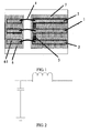
- an apparatus for improving transmission bandwidth includes: a signal transmission line 1, side grounds 2 located at two sides of the signal transmission line 1, and a capacitor 3 located between the signal transmission line 1 and the side grounds 2.
- the signal transmission line may be a microstrip line, and the signal transmission line and the side grounds form a coplanar waveguide transmission line together.
- the apparatus for improving transmission bandwidth may be applied to a transmission channel connected through a bonding wire.
- the signal transmission line 1 and the side grounds 2 are disposed on a substrate 7 having an optical component, an electric component or a photoelectric component, where the substrate 7 and a pad 61 of a package 6 are connected through a bonding wire 4.
- FIG. 2 is a schematic circuit diagram of the apparatus for improving transmission bandwidth, the bonding wire 4 presents inductance characteristics and is equivalent to an inductor.
- an LC resonance circuit is formed by using the inductance characteristics presented by the bonding wire 4 and the capacitor connected in parallel with the bonding wire 4, and a resonance point is formed within a frequency band in a frequency domain, so that a rising trend of a return loss curve is forced to slow down, thereby expanding frequency bandwidth and further expanding bandwidth of the transmission channel of a Radio Frequency (RF) signal.
- RF Radio Frequency
- the pad of the package may be a pad of an electrical interface of the photoelectric component package.
- the signal transmission line and the side grounds may be disposed on the package, for example, the signal transmission line and the side grounds may be disposed on the pad inside the package.
- the signal transmission line 1, the side grounds 2 and the capacitor 3 are disposed on the substrate 7, and moreover, the transmission line 1, the side grounds 2 and the capacitor 3 are also disposed on the package 6.
- the substrate 7 and the package 6 are connected through the bonding wire 4.
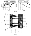
- FIG. 3 is a transmission channel connected through the bonding wire, and shows a change of a cut-off frequency point of a return loss of -10 dB before and after the capacitor is added, and a condition of insertion loss being reduced after the capacitor is adopted.
- m1 and m3 are conditions that no capacitor is disposed; m2 and m4 are conditions that an interdigital capacitor is disposed. It can be seen from FIG.
- the capacitor may be a plate capacitor, an interdigital capacitor, an MIM capacitor, or a VIC.
- the VIC when the capacitor is a VIC, the VIC includes multiple layers of metal surfaces.
- the multiple layers of metal surfaces overlap each other, and are respectively located on multiple metal conductor layers inside the substrate, where the multiple layers of metal surfaces that overlap each other form two electrodes of the VIC, and the metal surface on a top layer of the VIC is located at the same metal conductor layer with the signal transmission line.
- the multiple layers of metal surfaces located at one electrode of the VIC are connected via a through hole, and are connected to the side grounds; and the multiple layers of metal surfaces located at the other electrode of the VIC are connected to the metal surface on the top layer of the VIC via a through hole, and are connected to the signal transmission line.
- the capacitor may be integrated inside the substrate, which does not increase the area or the cost of the substrate. Moreover, the capacitor does not need to be assembled subsequently, and the capacity of the capacitor does not change with change of the external environment.
- the capacitor when the capacitor is disposed between the signal transmission line and the side grounds, if the signal transmission line or a side ground is connected to a pad, the capacitor may be connected to the signal transmission line or the side ground by being connected to the pad, thereby forming an LC resonance circuit with the bonding wire connected to the pad.
- adding the capacitor may also increase the area of the pad of the bonding wire, so that when multiple bonding wires are disposed, the distance between the bonding wires may be further increased, and the total inductance of all bonding wires connected between the substrate and the package may be reduced, thereby further improving the bandwidth of the transmission channel.
- the operation and control can be carried out more conveniently, and an error is not easily incurred, when multiple bonding wires need to be connected.
- the signal transmission line 1 and the second pad 92 (such as a signal pad) of the optical component 9 are not in the same plane, the signal transmission line 1 and the second pad 92 of the optical component 9 need to be connected through the bonding wire 4.
- the capacitor 3 may be disposed in parallel with the matching resistor 8 and disposed between the signal transmission line 1 and the side grounds 2, thereby expanding the bandwidth of the transmission channel.
- the apparatus for improving transmission bandwidth may be disposed on a TOSA, a Receiver Optical Sub-Assembly (ROSA), a Bidirectional Optical Sub-Assembly (BOSA) or a Balance Receiver (BLRX) and so on.
- the TOSA, ROSA, BOSA or BLRX may be located on the following communication devices: a 10 Gigabit Small Form Factor Pluggable Module (XFP), a Small Form Factor Pluggable Module plus (SFP+), or a 300PIN transponder.
Landscapes
- Waveguides (AREA)
- Semiconductor Lasers (AREA)
- Structure Of Printed Boards (AREA)
- Semiconductor Integrated Circuits (AREA)
- Optical Modulation, Optical Deflection, Nonlinear Optics, Optical Demodulation, Optical Logic Elements (AREA)
Abstract
Description
- The present invention relates to the field of electronic communications technologies, and in particular, to an apparatus for improving transmission bandwidth.
- In a photoelectric conversion module of a conventional photoelectric component such as a Transmitter Optical Sub-Assembly (TOSA), a substrate and a package are connected through a bonding wire, thereby implementing signal transmission.
- During the implementation of the present invention, the inventor finds that the prior art at least has the following defects.
- As the bonding wire present certain inductance characteristics, the impedance of a transmission channel is discontinuous, and the transmission bandwidth is greatly restricted.
- Embodiments of the present invention provide an apparatus for improving transmission bandwidth, the apparatus is disposed on a transmission channel connected through a bonding wire, and a capacitor is disposed between a signal transmission line and side grounds, thereby expanding the bandwidth of the transmission channel.
- The embodiments of the present invention adopt the following technical solutions.
- An apparatus for improving transmission bandwidth includes: a signal transmission line, side grounds located at two sides of the signal transmission line, and a capacitor disposed between the signal transmission line and the side grounds, where the signal transmission line is a microstrip line, and the signal transmission line and the side grounds form a coplanar waveguide transmission line together.
- A communication device includes a substrate, a package, and an apparatus for improving transmission bandwidth, where the apparatus for improving transmission bandwidth is disposed on the substrate or the package, or both the substrate and the package are disposed with the apparatus for improving transmission bandwidth; and the apparatus for improving transmission bandwidth includes: a signal transmission line, side grounds located at two sides of the signal transmission line, and a capacitor disposed between the signal transmission line and the side grounds, the signal transmission line is a microstrip line, and the signal transmission line and the side grounds form a coplanar waveguide transmission line together.
- The above technical solutions have the following advantages.
- In the embodiments of the present invention, on a transmission channel connected through a bonding wire, a capacitor is disposed between a signal transmission line and side grounds. An inductor-capacitor (LC) resonance circuit is formed by using inductance characteristics presented by the bonding wire and the capacitor connected in parallel with the bonding wire, and a resonance point is formed within a frequency band in a frequency domain, so that a rising trend of a return loss curve is forced to slow down, thereby expanding frequency bandwidth and further expanding bandwidth of a transmission channel of Radio Frequency (RF) signal.
- To illustrate the technical solutions according to the embodiments of the present invention or in the prior art more clearly, the accompanying drawings required for describing the embodiments or the prior art are introduced below briefly. Apparently, the accompanying drawings in the following descriptions merely show some of the embodiments of the present invention, and persons of ordinary skill in the art can obtain other drawings according to the accompanying drawings without creative efforts.
-
FIG 1 is a schematic diagram of an apparatus for improving transmission bandwidth according to an embodiment of the present invention; -
FIG. 2 is a schematic circuit diagram of an apparatus for improving transmission bandwidth according to the present invention; -
FIG. 3 is a schematic diagram of a return loss curve effect of an apparatus for improving transmission bandwidth according to the present invention; -
FIG. 4 is a schematic diagram of an apparatus for improving transmission bandwidth located on a substrate according to the present invention; -
FIG. 5 is a schematic diagram of a Metal Insulation Metal (MIM) capacitor adopted in an apparatus for improving transmission bandwidth according to the present invention; -
FIG. 6 is a schematic diagram of a Vertical Interdigital Capacitor (VIC) adopted in an apparatus for improving transmission bandwidth according to the present invention; -
FIG. 7 is a schematic diagram of an application scenario of an apparatus for improving transmission bandwidth according to the present invention; and -
FIG. 8 is a schematic diagram of another application scenario of an apparatus for improving transmission bandwidth according to the present invention. - The technical solutions of the present invention will be clearly and comprehensively described in the following with reference to the accompanying drawings. It is obvious that the embodiments to be described are only a part rather than all of the embodiments of the present invention. All other embodiments obtained by persons of ordinary skill in the art based on the embodiments of the present invention without creative efforts shall fall within the protection scope of the present invention.
- As shown in
FIG. 1 , an apparatus for improving transmission bandwidth according to an embodiment of the present invention includes: asignal transmission line 1,side grounds 2 located at two sides of thesignal transmission line 1, and acapacitor 3 located between thesignal transmission line 1 and theside grounds 2. - In the embodiment of the present invention, the signal transmission line may be a microstrip line, and the signal transmission line and the side grounds form a coplanar waveguide transmission line together.
- The apparatus for improving transmission bandwidth according to the embodiment of the present invention may be applied to a transmission channel connected through a bonding wire. For example, as shown in
FIG. 1 , thesignal transmission line 1 and theside grounds 2 are disposed on asubstrate 7 having an optical component, an electric component or a photoelectric component, where thesubstrate 7 and apad 61 of apackage 6 are connected through abonding wire 4. Referring toFIG. 2, FIG. 2 is a schematic circuit diagram of the apparatus for improving transmission bandwidth, thebonding wire 4 presents inductance characteristics and is equivalent to an inductor. By adding a capacitor with proper capacity at the substrate in a photoelectric component package or the pad in the package and connecting the capacitor in parallel to the ground, an LC resonance circuit is formed by using the inductance characteristics presented by thebonding wire 4 and the capacitor connected in parallel with thebonding wire 4, and a resonance point is formed within a frequency band in a frequency domain, so that a rising trend of a return loss curve is forced to slow down, thereby expanding frequency bandwidth and further expanding bandwidth of the transmission channel of a Radio Frequency (RF) signal. In this way, a higher signal transmission rate is achieved, and an insertion loss of the entire transmission channel is reduced at the same time (referring toFIG. 3 ). - In the embodiment of the present invention, the pad of the package may be a pad of an electrical interface of the photoelectric component package. In addition, the signal transmission line and the side grounds may be disposed on the package, for example, the signal transmission line and the side grounds may be disposed on the pad inside the package. Alternatively, as shown in
FIG. 4 , thesignal transmission line 1, theside grounds 2 and thecapacitor 3 are disposed on thesubstrate 7, and moreover, thetransmission line 1, theside grounds 2 and thecapacitor 3 are also disposed on thepackage 6. Thesubstrate 7 and thepackage 6 are connected through thebonding wire 4. -
FIG. 3 is a transmission channel connected through the bonding wire, and shows a change of a cut-off frequency point of a return loss of -10 dB before and after the capacitor is added, and a condition of insertion loss being reduced after the capacitor is adopted. InFIG. 3 , m1 and m3 are conditions that no capacitor is disposed; m2 and m4 are conditions that an interdigital capacitor is disposed. It can be seen fromFIG. 3 that by disposing a capacitor, a return loss curve of the transmission channel forms a resonance point in a valid bandwidth, so that a cut-off frequency of the transmission channel with a return loss smaller than -10 dB is increased from 5.3 GHz to 23.4 GHz, thereby greatly expanding the transmission bandwidth, and further enabling the transmission channel to transmit a signal at a higher rate. - In the embodiment of the present invention, the capacitor may be a plate capacitor, an interdigital capacitor, an MIM capacitor, or a VIC.
- As shown in
FIG. 5 , when the capacitor is an MIM capacitor, the MIM capacitor includes a top layer metal surface and a bottom layer metal surface, where the top layer metal surface and the bottom layer metal surface are respectively disposed on two metal conductor layers inside the substrate, and the top layer metal surface is located at the same metal conductor layer with the signal transmission line. The bottom layer metal surface is connected to the top layer metal surface via a through hole, and is connected to the side grounds. The top layer metal surface is connected to the signal transmission line. - As shown in
FIG. 6 , when the capacitor is a VIC, the VIC includes multiple layers of metal surfaces. The multiple layers of metal surfaces overlap each other, and are respectively located on multiple metal conductor layers inside the substrate, where the multiple layers of metal surfaces that overlap each other form two electrodes of the VIC, and the metal surface on a top layer of the VIC is located at the same metal conductor layer with the signal transmission line. The multiple layers of metal surfaces located at one electrode of the VIC are connected via a through hole, and are connected to the side grounds; and the multiple layers of metal surfaces located at the other electrode of the VIC are connected to the metal surface on the top layer of the VIC via a through hole, and are connected to the signal transmission line. - In the embodiment of the present invention, the capacitor may be integrated inside the substrate, which does not increase the area or the cost of the substrate. Moreover, the capacitor does not need to be assembled subsequently, and the capacity of the capacitor does not change with change of the external environment.
- In the embodiment of the present invention, when the capacitor is disposed between the signal transmission line and the side grounds, if the signal transmission line or a side ground is connected to a pad, the capacitor may be connected to the signal transmission line or the side ground by being connected to the pad, thereby forming an LC resonance circuit with the bonding wire connected to the pad. In this way, if the capacitor is connected to the pad, adding the capacitor may also increase the area of the pad of the bonding wire, so that when multiple bonding wires are disposed, the distance between the bonding wires may be further increased, and the total inductance of all bonding wires connected between the substrate and the package may be reduced, thereby further improving the bandwidth of the transmission channel.
- Further, if the area of the pad of the bonding wire is increased, the operation and control can be carried out more conveniently, and an error is not easily incurred, when multiple bonding wires need to be connected.
-
FIG. 7 shows another application scenario of an apparatus for improving transmission bandwidth according to an embodiment of the present invention. An optical component, an electric component or a photoelectric component 9 is disposed on a substrate, where the optical component, the electric component or the photoelectric component 9 is soldered to the substrate through afirst pad 91, asecond pad 92 of the optical component, the electric component or the photoelectric component 9 is connected to asignal transmission line 1 disposed on the substrate through abonding wire 4, and acapacitor 3 is disposed between thesignal transmission line 1 andside grounds 2, thereby expanding the transmission bandwidth. For example, when amatching resistor 8 on the substrate is away from the optical component 9 matched with thematching resistor 8, thematching resistor 8 and the optical component 9 are connected through thesignal transmission line 1. Moreover, as thesignal transmission line 1 and the second pad 92 (such as a signal pad) of the optical component 9 are not in the same plane, thesignal transmission line 1 and thesecond pad 92 of the optical component 9 need to be connected through thebonding wire 4. At this time, thecapacitor 3 may be disposed in parallel with thematching resistor 8 and disposed between thesignal transmission line 1 and theside grounds 2, thereby expanding the bandwidth of the transmission channel. - As shown in
FIG 8 , the apparatus for improving transmission bandwidth according to the embodiment of the present invention may be disposed on a TOSA, a Receiver Optical Sub-Assembly (ROSA), a Bidirectional Optical Sub-Assembly (BOSA) or a Balance Receiver (BLRX) and so on. The TOSA, ROSA, BOSA or BLRX may be located on the following communication devices: a 10 Gigabit Small Form Factor Pluggable Module (XFP), a Small Form Factor Pluggable Module plus (SFP+), or a 300PIN transponder. - Only several embodiments of the present invention have been described above. Persons skilled in the art can make various modifications and variations to the present invention according to the disclosure of the application document without departing from the spirit and scope of the present invention.
Claims (13)
- An apparatus for improving transmission bandwidth, comprising: a signal transmission line, side grounds located at two sides of the signal transmission line, and a capacitor disposed between the signal transmission line and the side grounds, wherein the signal transmission line is a microstrip line, and the signal transmission line and the side grounds form a coplanar waveguide transmission line together.
- The apparatus according to claim 1, wherein the signal transmission line and the side grounds are disposed on a substrate, and the substrate and a pad of a package are connected through a bonding wire.
- The apparatus according to claim 1, wherein the signal transmission line and the side grounds are disposed on a pad inside a package, and the pad inside the package and a substrate are connected through a bonding wire.
- The apparatus according to claim 1, wherein the signal transmission line, the side grounds and the capacitor are disposed on a substrate, the signal transmission line, the side grounds and the capacitor are also disposed on a package, and the substrate and the package are connected through bonding wire.
- The apparatus according to claim 1, wherein the capacitor is an interdigital capacitor.
- The apparatus according to claim 1, wherein the signal transmission line and the side grounds are disposed on a substrate, the capacitor is a Metal Insulation Metal (MIM) capacitor, the MIM capacitor comprises a top layer metal surface and a bottom layer metal surface, the top layer metal surface and the bottom layer metal surface are respectively disposed on two metal conductor layers inside the substrate, the top layer metal surface is located at the same metal conductor layer with the signal transmission line, the bottom layer metal surface is connected to the top layer metal surface via a through hole, and is connected to the side grounds; and the top layer metal surface is connected to the signal transmission line.
- The apparatus according to claim 1, wherein the signal transmission line and the side grounds are disposed on a substrate, the capacitor is a Vertical Interdigital Capacitor (VIC), and the VIC comprises multiple layers of metal surfaces; the multiple layers of metal surfaces overlap each other, and are respectively located on multiple metal conductor layers inside the substrate; the multiple layers of metal surfaces that overlap each other form two electrodes of the VIC, the metal surface on a top layer of the VIC is located at the same metal conductor layer with the signal transmission line; the multiple layers of metal surfaces located at one electrode of the VIC are connected via a through hole, and are connected to the side grounds; and the multiple layers of metal surfaces located at the other electrode of the VIC are connected to the metal surface on the top layer of the VIC via a through hole, and are connected to the signal transmission line.
- The apparatus according to claim 1, wherein the signal transmission line or a side ground is connected to a pad, and the capacitor is connected to the signal transmission line or the side ground by being connected to the pad.
- The apparatus according to claim 1, wherein the signal transmission line and the side grounds are disposed on a substrate having an optical component, an electric component or a photoelectric component, the optical component, the electric component or the photoelectric component is soldered to the substrate through a first pad, and a second pad of the optical component, the electric component or the photoelectric component is connected to the signal transmission line through a bonding wire.
- The apparatus according to claim 1, wherein the signal transmission line and the side grounds are disposed on a substrate having an optical component, an electric component or a photoelectric component, a matching resistor on the substrate and the optical component matched with the matching resistor are connected through the signal transmission line, and the signal transmission line and a second pad of the optical component are connected through a bonding wire.
- A communication device, comprising a substrate, a package, and the apparatus for improving transmission bandwidth according to any one of claims 1 to 10, wherein the apparatus for improving transmission bandwidth is disposed on the substrate or the package, or, both the substrate and the package are disposed with the apparatus for improving transmission bandwidth.
- The communication device according to claim 11, wherein the communication device is disposed with a Transmitter Optical Sub-Assembly (TOSA), a Receiver Optical Sub-Assembly (ROSA), a Bidirectional Optical Sub-Assembly (BOSA) or a Balance Receiver (BLRX), and the substrate and the package are located on the TOSA, the ROSA, the BOSA or the BLRX.
- The communication device according to claim 11, wherein the communication device is a 10 Gigabit Small Form Factor Pluggable Module (XFP), a Small Form Factor Pluggable Module plus (SFP+) or a 300PIN transponder.
Applications Claiming Priority (2)
| Application Number | Priority Date | Filing Date | Title |
|---|---|---|---|
| CN200910189398.7A CN101794929B (en) | 2009-12-26 | 2009-12-26 | Device for improving transmission bandwidth |
| PCT/CN2010/079745 WO2011076068A1 (en) | 2009-12-26 | 2010-12-14 | Apparatus for improving transmission bandwidth |
Publications (2)
| Publication Number | Publication Date |
|---|---|
| EP2432071A1 true EP2432071A1 (en) | 2012-03-21 |
| EP2432071A4 EP2432071A4 (en) | 2012-06-13 |
Family
ID=42587420
Family Applications (1)
| Application Number | Title | Priority Date | Filing Date |
|---|---|---|---|
| EP10838631A Ceased EP2432071A4 (en) | 2009-12-26 | 2010-12-14 | Apparatus for improving transmission bandwidth |
Country Status (4)
| Country | Link |
|---|---|
| US (1) | US8558645B2 (en) |
| EP (1) | EP2432071A4 (en) |
| CN (1) | CN101794929B (en) |
| WO (1) | WO2011076068A1 (en) |
Cited By (1)
| Publication number | Priority date | Publication date | Assignee | Title |
|---|---|---|---|---|
| WO2020219173A1 (en) * | 2019-04-24 | 2020-10-29 | Raytheon Company | Frequency selective capacitively tuned ground bonds for high isolation in rf devices |
Families Citing this family (9)
| Publication number | Priority date | Publication date | Assignee | Title |
|---|---|---|---|---|
| CN101794929B (en) | 2009-12-26 | 2013-01-02 | 华为技术有限公司 | Device for improving transmission bandwidth |
| US9979388B2 (en) | 2013-11-07 | 2018-05-22 | Nxp Usa, Inc. | Adjustable losses of bond wire arrangement |
| US9692386B2 (en) | 2013-12-23 | 2017-06-27 | Qualcomm Incorporated | Three-dimensional wire bond inductor |
| CN104767103B (en) | 2015-03-30 | 2017-12-19 | 青岛海信宽带多媒体技术有限公司 | A kind of laser attachment structure and laser assembly |
| CN104836619B (en) * | 2015-03-30 | 2017-08-29 | 青岛海信宽带多媒体技术有限公司 | A kind of optical device |
| WO2020056662A1 (en) * | 2018-09-20 | 2020-03-26 | 华为技术有限公司 | Photoelectron component and manufacturing method therefor |
| CN213342769U (en) * | 2019-12-31 | 2021-06-01 | 华为机器有限公司 | Light emitting module, semiconductor optoelectronic device and apparatus |
| CN112040643B (en) * | 2020-09-23 | 2024-01-30 | 北京安石科技有限公司 | High-speed signal link design adopting parallel capacitors |
| CN115831936B (en) * | 2021-09-16 | 2023-09-05 | 安徽奥飞声学科技有限公司 | Substrate with buried capacitor and buried capacitor testing method thereof |
Citations (4)
| Publication number | Priority date | Publication date | Assignee | Title |
|---|---|---|---|---|
| US5777532A (en) * | 1997-01-15 | 1998-07-07 | Tfr Technologies, Inc. | Interdigital slow wave coplanar transmission line |
| US6242992B1 (en) * | 1999-07-30 | 2001-06-05 | Tfr Technologies, Inc. | Interdigital slow-wave coplanar transmission line resonator and coupler |
| US20040070811A1 (en) * | 2002-10-10 | 2004-04-15 | Opnext Japan, Inc. | Transmission line, optical module using the same and manufacturing method of optical module |
| US20040207432A1 (en) * | 2003-02-24 | 2004-10-21 | Kanji Otsuka | Electronic circuit device |
Family Cites Families (9)
| Publication number | Priority date | Publication date | Assignee | Title |
|---|---|---|---|---|
| US3593208A (en) * | 1969-03-17 | 1971-07-13 | Bell Telephone Labor Inc | Microwave quadrature coupler having lumped-element capacitors |
| US4600907A (en) * | 1985-03-07 | 1986-07-15 | Tektronix, Inc. | Coplanar microstrap waveguide interconnector and method of interconnection |
| US5485131A (en) * | 1994-10-13 | 1996-01-16 | Motorola, Inc. | Transmission line filter for MIC and MMIC applications |
| US6057954A (en) | 1998-09-18 | 2000-05-02 | Lucent Technologies Inc. | Asymmetric inductive peaking for optoelectronic devices |
| GB0128418D0 (en) | 2001-11-28 | 2002-01-16 | Koninl Philips Electronics Nv | Dual-band antenna arrangement |
| US7061949B1 (en) | 2002-08-16 | 2006-06-13 | Jds Uniphase Corporation | Methods, apparatus, and systems with semiconductor laser packaging for high modulation bandwidth |
| CN100442596C (en) * | 2005-07-29 | 2008-12-10 | 华东师范大学 | Aperiodic capacity loaded phase shifter |
| CN100511827C (en) * | 2005-09-29 | 2009-07-08 | 中国科学院物理研究所 | Ferroelectric thin-membrane phase shifter, and method for detecting and optimizing reflection characteristics |
| CN101794929B (en) * | 2009-12-26 | 2013-01-02 | 华为技术有限公司 | Device for improving transmission bandwidth |
-
2009
- 2009-12-26 CN CN200910189398.7A patent/CN101794929B/en active Active
-
2010
- 2010-12-14 EP EP10838631A patent/EP2432071A4/en not_active Ceased
- 2010-12-14 WO PCT/CN2010/079745 patent/WO2011076068A1/en active Application Filing
-
2011
- 2011-12-02 US US13/310,408 patent/US8558645B2/en active Active
Patent Citations (4)
| Publication number | Priority date | Publication date | Assignee | Title |
|---|---|---|---|---|
| US5777532A (en) * | 1997-01-15 | 1998-07-07 | Tfr Technologies, Inc. | Interdigital slow wave coplanar transmission line |
| US6242992B1 (en) * | 1999-07-30 | 2001-06-05 | Tfr Technologies, Inc. | Interdigital slow-wave coplanar transmission line resonator and coupler |
| US20040070811A1 (en) * | 2002-10-10 | 2004-04-15 | Opnext Japan, Inc. | Transmission line, optical module using the same and manufacturing method of optical module |
| US20040207432A1 (en) * | 2003-02-24 | 2004-10-21 | Kanji Otsuka | Electronic circuit device |
Non-Patent Citations (1)
| Title |
|---|
| See also references of WO2011076068A1 * |
Cited By (1)
| Publication number | Priority date | Publication date | Assignee | Title |
|---|---|---|---|---|
| WO2020219173A1 (en) * | 2019-04-24 | 2020-10-29 | Raytheon Company | Frequency selective capacitively tuned ground bonds for high isolation in rf devices |
Also Published As
| Publication number | Publication date |
|---|---|
| US8558645B2 (en) | 2013-10-15 |
| CN101794929A (en) | 2010-08-04 |
| WO2011076068A1 (en) | 2011-06-30 |
| US20120075042A1 (en) | 2012-03-29 |
| EP2432071A4 (en) | 2012-06-13 |
| CN101794929B (en) | 2013-01-02 |
Similar Documents
| Publication | Publication Date | Title |
|---|---|---|
| US8558645B2 (en) | Apparatus for improving transmission bandwidth | |
| US9159634B2 (en) | Transistor outline housing and method for producing same | |
| US9413335B2 (en) | High-frequency module | |
| CN101533939B (en) | Collaboratively designed double frequency-band antenna-filter device | |
| KR101119910B1 (en) | Mobile RFID Reader Transceiver System | |
| KR101222257B1 (en) | Multilayer substrate | |
| US11245386B2 (en) | High-frequency module | |
| US20120062332A1 (en) | Variable capacitance module and matching circuit module | |
| KR20120105264A (en) | Structure of transmission line for data communication, and method for designing of the said line | |
| EP3327859B1 (en) | Directional coupler and communication module | |
| CN102355223B (en) | Single-chip GSM (Global System for Mobile Communications) radio-frequency antenna switch module and GSM radio-frequency front end | |
| US8060156B2 (en) | Filter having impedance matching circuits | |
| US9461619B2 (en) | High-frequency module | |
| CN100382466C (en) | Optical receiver module with to-can structure | |
| JP2015133660A (en) | Integrated circuit and transceiver device | |
| JP2013229801A (en) | Optical reception module and optical receiver | |
| CN115933070B (en) | Optical module and laser assembly | |
| JP3916072B2 (en) | AC coupling circuit | |
| JP5112962B2 (en) | package | |
| KR20090069411A (en) | Directional coupler and duplex transceiver system in package | |
| JP5720261B2 (en) | Electronic circuit and transmission / reception system | |
| US11722115B2 (en) | Radio frequency duplexer circuit and radio frequency substrate | |
| KR100714598B1 (en) | Directional coupler and composite device comprising the same | |
| CN101272153A (en) | Signal receiving circuit to transmit high speed signal | |
| JP4969193B2 (en) | Duplexer |
Legal Events
| Date | Code | Title | Description |
|---|---|---|---|
| PUAI | Public reference made under article 153(3) epc to a published international application that has entered the european phase |
Free format text: ORIGINAL CODE: 0009012 |
|
| 17P | Request for examination filed |
Effective date: 20111203 |
|
| AK | Designated contracting states |
Kind code of ref document: A1 Designated state(s): AL AT BE BG CH CY CZ DE DK EE ES FI FR GB GR HR HU IE IS IT LI LT LU LV MC MK MT NL NO PL PT RO RS SE SI SK SM TR |
|
| A4 | Supplementary search report drawn up and despatched |
Effective date: 20120516 |
|
| RIC1 | Information provided on ipc code assigned before grant |
Ipc: H01P 3/08 20060101AFI20120510BHEP |
|
| DAX | Request for extension of the european patent (deleted) | ||
| 17Q | First examination report despatched |
Effective date: 20131206 |
|
| REG | Reference to a national code |
Ref country code: DE Ref legal event code: R003 |
|
| STAA | Information on the status of an ep patent application or granted ep patent |
Free format text: STATUS: THE APPLICATION HAS BEEN REFUSED |
|
| 18R | Application refused |
Effective date: 20180129 |