EP2432032A2 - Solar cell module and laminating method - Google Patents
Solar cell module and laminating method Download PDFInfo
- Publication number
- EP2432032A2 EP2432032A2 EP11179151A EP11179151A EP2432032A2 EP 2432032 A2 EP2432032 A2 EP 2432032A2 EP 11179151 A EP11179151 A EP 11179151A EP 11179151 A EP11179151 A EP 11179151A EP 2432032 A2 EP2432032 A2 EP 2432032A2
- Authority
- EP
- European Patent Office
- Prior art keywords
- metal foil
- foil line
- sub
- photoelectric conversion
- line
- Prior art date
- Legal status (The legal status is an assumption and is not a legal conclusion. Google has not performed a legal analysis and makes no representation as to the accuracy of the status listed.)
- Withdrawn
Links
Images

Classifications
-
- H—ELECTRICITY
- H10—SEMICONDUCTOR DEVICES; ELECTRIC SOLID-STATE DEVICES NOT OTHERWISE PROVIDED FOR
- H10F—INORGANIC SEMICONDUCTOR DEVICES SENSITIVE TO INFRARED RADIATION, LIGHT, ELECTROMAGNETIC RADIATION OF SHORTER WAVELENGTH OR CORPUSCULAR RADIATION
- H10F77/00—Constructional details of devices covered by this subclass
- H10F77/93—Interconnections
- H10F77/933—Interconnections for devices having potential barriers
- H10F77/935—Interconnections for devices having potential barriers for photovoltaic devices or modules
- H10F77/937—Busbar structures for modules
-
- H—ELECTRICITY
- H10—SEMICONDUCTOR DEVICES; ELECTRIC SOLID-STATE DEVICES NOT OTHERWISE PROVIDED FOR
- H10F—INORGANIC SEMICONDUCTOR DEVICES SENSITIVE TO INFRARED RADIATION, LIGHT, ELECTROMAGNETIC RADIATION OF SHORTER WAVELENGTH OR CORPUSCULAR RADIATION
- H10F19/00—Integrated devices, or assemblies of multiple devices, comprising at least one photovoltaic cell covered by group H10F10/00, e.g. photovoltaic modules
- H10F19/30—Integrated devices, or assemblies of multiple devices, comprising at least one photovoltaic cell covered by group H10F10/00, e.g. photovoltaic modules comprising thin-film photovoltaic cells
- H10F19/31—Integrated devices, or assemblies of multiple devices, comprising at least one photovoltaic cell covered by group H10F10/00, e.g. photovoltaic modules comprising thin-film photovoltaic cells having multiple laterally adjacent thin-film photovoltaic cells deposited on the same substrate
- H10F19/35—Structures for the connecting of adjacent photovoltaic cells, e.g. interconnections or insulating spacers
-
- H—ELECTRICITY
- H10—SEMICONDUCTOR DEVICES; ELECTRIC SOLID-STATE DEVICES NOT OTHERWISE PROVIDED FOR
- H10F—INORGANIC SEMICONDUCTOR DEVICES SENSITIVE TO INFRARED RADIATION, LIGHT, ELECTROMAGNETIC RADIATION OF SHORTER WAVELENGTH OR CORPUSCULAR RADIATION
- H10F19/00—Integrated devices, or assemblies of multiple devices, comprising at least one photovoltaic cell covered by group H10F10/00, e.g. photovoltaic modules
- H10F19/90—Structures for connecting between photovoltaic cells, e.g. interconnections or insulating spacers
- H10F19/902—Structures for connecting between photovoltaic cells, e.g. interconnections or insulating spacers for series or parallel connection of photovoltaic cells
-
- H—ELECTRICITY
- H10—SEMICONDUCTOR DEVICES; ELECTRIC SOLID-STATE DEVICES NOT OTHERWISE PROVIDED FOR
- H10F—INORGANIC SEMICONDUCTOR DEVICES SENSITIVE TO INFRARED RADIATION, LIGHT, ELECTROMAGNETIC RADIATION OF SHORTER WAVELENGTH OR CORPUSCULAR RADIATION
- H10F77/00—Constructional details of devices covered by this subclass
- H10F77/10—Semiconductor bodies
- H10F77/16—Material structures, e.g. crystalline structures, film structures or crystal plane orientations
- H10F77/169—Thin semiconductor films on metallic or insulating substrates
- H10F77/1698—Thin semiconductor films on metallic or insulating substrates the metallic or insulating substrates being flexible
-
- H—ELECTRICITY
- H10—SEMICONDUCTOR DEVICES; ELECTRIC SOLID-STATE DEVICES NOT OTHERWISE PROVIDED FOR
- H10F—INORGANIC SEMICONDUCTOR DEVICES SENSITIVE TO INFRARED RADIATION, LIGHT, ELECTROMAGNETIC RADIATION OF SHORTER WAVELENGTH OR CORPUSCULAR RADIATION
- H10F77/00—Constructional details of devices covered by this subclass
- H10F77/20—Electrodes
- H10F77/206—Electrodes for devices having potential barriers
- H10F77/211—Electrodes for devices having potential barriers for photovoltaic cells
- H10F77/219—Arrangements for electrodes of back-contact photovoltaic cells
- H10F77/227—Arrangements for electrodes of back-contact photovoltaic cells for emitter wrap-through [EWT] photovoltaic cells, e.g. interdigitated emitter-base back-contacts
-
- Y—GENERAL TAGGING OF NEW TECHNOLOGICAL DEVELOPMENTS; GENERAL TAGGING OF CROSS-SECTIONAL TECHNOLOGIES SPANNING OVER SEVERAL SECTIONS OF THE IPC; TECHNICAL SUBJECTS COVERED BY FORMER USPC CROSS-REFERENCE ART COLLECTIONS [XRACs] AND DIGESTS
- Y02—TECHNOLOGIES OR APPLICATIONS FOR MITIGATION OR ADAPTATION AGAINST CLIMATE CHANGE
- Y02E—REDUCTION OF GREENHOUSE GAS [GHG] EMISSIONS, RELATED TO ENERGY GENERATION, TRANSMISSION OR DISTRIBUTION
- Y02E10/00—Energy generation through renewable energy sources
- Y02E10/50—Photovoltaic [PV] energy
-
- Y—GENERAL TAGGING OF NEW TECHNOLOGICAL DEVELOPMENTS; GENERAL TAGGING OF CROSS-SECTIONAL TECHNOLOGIES SPANNING OVER SEVERAL SECTIONS OF THE IPC; TECHNICAL SUBJECTS COVERED BY FORMER USPC CROSS-REFERENCE ART COLLECTIONS [XRACs] AND DIGESTS
- Y10—TECHNICAL SUBJECTS COVERED BY FORMER USPC
- Y10T—TECHNICAL SUBJECTS COVERED BY FORMER US CLASSIFICATION
- Y10T156/00—Adhesive bonding and miscellaneous chemical manufacture
- Y10T156/10—Methods of surface bonding and/or assembly therefor
- Y10T156/1002—Methods of surface bonding and/or assembly therefor with permanent bending or reshaping or surface deformation of self sustaining lamina
- Y10T156/1051—Methods of surface bonding and/or assembly therefor with permanent bending or reshaping or surface deformation of self sustaining lamina by folding
Definitions
- the present invention relates to a solar cell module and a laminating method, and more particularly, to a method of forming wiring lines of a solar cell module.
- amorphous silicon solar cells are promising in terms of productivity or costs.
- a flexible module has been developed in which photoelectric conversion elements are formed on a film substrate and the surfaces of the photoelectric conversion elements are covered with a protective film and an adhesive sheet.
- Internal wiring lines including a main wiring line and a sub-wiring line are used in order to extract power from the solar cell module covered with the protective film to the outside.
- the photoelectric conversion element in the solar cell module is connected to the sub-wiring line and the sub-wiring line is connected to the main wiring line.
- Portions of the protective film and the adhesive sheet arranged on the end of the main wiring line are removed such that the end of the main wiring line is exposed.
- the end of an external lead is soldered to the exposed portion (see Japanese Patent Application Laid-Open No. 10-173209 ).
- An object of the invention is to provide a solar cell module and a laminating method capable of connecting an internal wiring line to a photoelectric conversion element without damaging flexibility and facilitating the connection of an external wiring line to the internal wiring line.
- a solar cell module including: a plurality of sheet-shaped photoelectric conversion elements; sub-metal foil lines that are provided so as to come into contact with electrodes of the plurality of photoelectric conversion elements; a main metal foil line that is connected to the sub-metal foil line which is folded such that the main metal foil line is interposed between the folded portions and extracts power generated from the plurality of photoelectric conversion elements to the outside; and protective films and adhesive sheets that are provided so as to cover both surfaces of each of the plurality of photoelectric conversion elements together with the main metal foil line and the sub-metal foil lines.
- the length of the folded portion of the sub-metal foil line may be equal to or more than the width of the main metal foil line.
- the main metal foil line is reliably interposed between the folded portions of the sub-metal foil line and it is possible to reliably connect the main metal foil line and the sub-metal foil line.
- the folded portion of the sub-metal foil line may be fixed to the electrode by an adhesive tape. According to this structure, it is possible to reliably fix the sub-metal foil line to the electrode and prevent the main metal foil line from being taken off from the interposed portion.
- the solar cell module according to the third aspect only a part of the folded portion of the sub-metal foil line that does not overlap the main metal foil line may be fixed to the electrode by the adhesive tape. According to this structure, it is possible to reliably ensure flexibility in the positional relationship between the main metal foil line and the sub-metal foil line.
- a laminating method including: arranging sub-metal foil lines so as to come into contact with electrodes of a plurality of sheet-shaped photoelectric conversion elements; folding the sub-metal foil line such that a main metal foil line which extracts power generated from the plurality of photoelectric conversion elements to the outside is interposed between the folded portions, thereby connecting the main metal foil line to the sub-metal foil line; and sequentially laminating a first protective film, a first adhesive sheet, the photoelectric conversion elements including the sub-metal foil lines and the main metal foil line provided therein, a second adhesive sheet, and a second protective film, and performing a heat treatment to integrate the first protective film, the first adhesive sheet, the photoelectric conversion elements, the second adhesive sheet, and the second protective film.
- this structure it is possible to manufacture a structure in which a module including a plurality of sheet-shaped photoelectric conversion elements connected to each other by a main metal foil line and sub-metal foil lines is covered with a protective film
- a laminating method including: arranging sub-metal foil lines so as to come into contact with electrodes of a plurality of sheet-shaped photoelectric conversion elements; folding the sub-metal foil line such that a main metal foil line which extracts power generated from the plurality of photoelectric conversion elements to the outside is interposed between the folded portions, thereby connecting the main metal foil line to the sub-metal foil line; sequentially laminating a first protective film, a first adhesive sheet, the photoelectric conversion elements including the sub-metal foil lines and the main metal foil line whose end is folded provided therein, a second adhesive sheet, and a second protective film, and performing a heat treatment to integrate the first protective film, the first adhesive sheet, the photoelectric conversion elements, the second adhesive sheet, and the second protective film; and trimming the first protective film, the first adhesive film, the second protective film, and the second adhesive film together with the folded portion of the end of the main metal foil line.
- an external lead can be inserted into a gap formed by trimming the folded portion of the main metal foil line. Therefore, it is possible to extract power generated from a plurality of photoelectric conversion elements to the outside and easily connect the external lead and the main metal foil line.
- the laminating method according to the sixth aspect may further include: removing the folded portion of the end of the main metal foil line together with the first protective film and the first adhesive sheet, or the second protective film and the second adhesive sheet. According to this structure, it is possible to easily expose the main metal foil line without an insulator remaining on the surface of the main metal foil line.
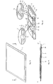
- FIGS. 1A to 1C are perspective views and a cross-sectional view schematically illustrating the structure of a solar cell module according to an embodiment of the invention.
- a plurality of photoelectric conversion elements 3 is bonded to a protective film 1 with an adhesive sheet 2 interposed therebetween and a protective film 5 is bonded to the photoelectric conversion elements 3 with an adhesive sheet 4 interposed therebetween.
- a main metal foil line 34 that extracts power from the photoelectric conversion elements 3 to the outside is arranged on the electrodes of the photoelectric conversion elements 3.
- a photoelectric conversion layer 13 is deposited on a film substrate 11 with a back electrode layer 12 interposed therebetween and a transparent electrode layer 14 is deposited on the photoelectric conversion layer 13.
- a rear electrode layer 15 is formed on the rear surface of the film substrate 11.
- a polyimide or polyamide resin film may be used as the film substrate 11
- a pin structure made of amorphous silicon may be used as the photoelectric conversion layer 13
- an ITO film may be used as the transparent electrode layer 14.
- Grooves 19 are formed in the rear electrode layer 15 to divide the rear electrode layer 15. Grooves 18 that divide the back electrode layer 12, the photoelectric conversion layer 13, and the transparent electrode layer 14 are formed in the back electrode layer 12, the photoelectric conversion layer 13, and the transparent electrode layer 14 such that they are in parallel to each other and alternate with the grooves 19. In this way, unit cells U1 to U4 are formed. In the film substrate 11, series holes 16 that connect the divided photoelectric conversion layers 13 in series to each other are formed in each of the unit cells U1 to U4. The rear electrode layer 15 and the back electrode layer 12 that are opposite to each other with the film substrate 11 interposed therebetween are connected to each other by the series holes 16.
- Power collection holes 17 that collect charge generated from the photoelectric conversion layers 13 to the rear electrode layer 15 are formed in the film substrate 11, the back electrode layer 12, and the rear electrode layer 15 for each of the unit cells U1 to U4.
- the transparent electrode layer 14 is connected to the rear electrode layer 15 through the power collection holes 17.
- the series holes 16 and the power collection holes 17 are arranged such that the series holes 16 in each of the unit cells U1 to U4 are connected to the rear electrode layer 15 that is provided immediately below the series holes 16 and the power collection holes 17 in each of the unit cells U1 to U4 are connected to the rear electrode layer 15 that is adjacent to the rear electrode layer 15 connected to the series holes 16.
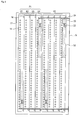
- sub-metal foil lines 33 are arranged so as to come into contact with the rear electrode layers 15 of photoelectric conversion elements P1 and P2.
- the sub-metal foil line 33 is fixed to the rear electrode layer 15 by an adhesive tape 32.
- the sub-metal foil line 33 is folded such that the main metal foil line 34 is interposed between the folded portions. In this way, the main metal foil line 34 is connected to the sub-metal foil line 33.
- the main metal foil line 34 extends to the end of the protective film 5.
- solder-coated copper foil lines may be used as the sub-metal foil line 33 and the main metal foil line 34.
- an insulating sheet may be provided below the main metal foil line 34 in the unit cells U1 to U4, or the main metal foil line 34 may be covered with an insulator, thereby ensuring the insulation between different unit cells U1 to U4.
- flexibility in the connection between the main metal foil line and the sub-metal foil line forming the internal wiring lines of the solar cell module is obtained and it is possible to absorb distortion occurring in the manufacture of the solar cell module. Therefore, it is possible to connect the internal wiring lines to a plurality of photoelectric conversion elements P1 and P2 without damaging the flexibility of the module.
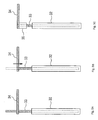
- Figs. 3A to 3C are plan views illustrating a method of connecting the sub-metal foil line 33 and the main metal foil line 34 of the solar cell module according to the embodiment of the invention.
- the main metal foil line 34 is superimposed on the sub-metal foil line 33 such that the main metal foil line 34 is orthogonal to the sub-metal foil line 33.
- the sub-metal foil line 33 is folded such that the folded portions of the sub-metal foil line 33 overlap each other with the main metal foil line 34 interposed therebetween. That is, the main metal foil line 34 is interposed between the folded portions of the sub-metal foil line 33 in the vertical direction.
- the main metal foil line 34 is reliably interposed between the folded portions.
- the length of the folded portion is 4 to 5 times more than the width of the main metal foil line 34
- the main metal foil line 34 is more reliably interposed between the folded portions and it is possible to prevent the main metal foil line 34 from being fixed by the adhesive tape 35 due to an error.
- the folded portion of the sub-metal foil line 33 is fixed to the rear electrode layer 15 by the adhesive tape 35. In this way, it is possible to prevent the main metal foil line 34 from being taken off from the folded portions of the sub-metal foil line 33.
- a metal foil label with a conductive adhesive is used as the adhesive tapes 32 and 35, it is possible to reliably connect the sub-metal foil line 33 and the rear electrode layer 15.
- Figs. 4A to 4E are plan views and a perspective view illustrating a method of connecting the main metal foil line 34 of the solar cell module according to the embodiment of the invention to the outside.
- the main metal foil line 34 is placed so as to extend to the outside of the photoelectric conversion element 3 shown in Figs. 1A to 1C , and the end of the main metal foil line 34 is folded such that the ends of the main metal foil line 34 overlap each other.
- the protective films 1 and 5 are placed on the photoelectric conversion element 3 and the main metal foil line 34 to seal the photoelectric conversion element 3 and the main metal foil line 34.
- Fig. 4A the main metal foil line 34 is placed so as to extend to the outside of the photoelectric conversion element 3 shown in Figs. 1A to 1C , and the end of the main metal foil line 34 is folded such that the ends of the main metal foil line 34 overlap each other.
- the protective films 1 and 5 are placed on the photoelectric conversion element 3 and the main metal foil line 34 to seal the photoelectric conversion element 3 and the main
- the protective films 1 and 5 are trimmed together with the end of the folded portion of the main metal foil line 34. Then, when the end of the folded portion of the main metal foil line 34 is removed together with the protective film 1 or 5 as shown in Fig. 4D , it is possible to easily expose the surface of the main metal foil line 34 to the outside.
- a crimp-type terminal 38 provided at an external lead 37 may be inserted into the gap between two folded main metal foil lines 34 without performing the process shown in Fig. 4D . In this case, it is also possible to connect the external lead line 37 and the main metal foil line 34.
Landscapes
- Photovoltaic Devices (AREA)
- Electroluminescent Light Sources (AREA)
Abstract
Disclosed is a technique capable of connecting internal wiring lines to a plurality of sheet-shaped photoelectric conversion elements without damaging flexibility. Sub-metal foil lines are arranged so as to come into contact with rear electrode layers of photoelectric conversion elements. The sub-metal foil line is fixed to the rear electrode layer by an adhesive tape. In addition, the sub-metal foil line is folded such that a main metal foil line is interposed between the folded portions of the sub-metal foil line. In this way, the main metal foil line is connected to the sub-metal foil line. The sub-metal foil line is fixed to the rear electrode layer by an adhesive tape.
Description
- The present invention relates to a solar cell module and a laminating method, and more particularly, to a method of forming wiring lines of a solar cell module.
- When solar cells are installed on the roof and then used, amorphous silicon solar cells are promising in terms of productivity or costs.
In the amorphous silicon solar cell, a flexible module has been developed in which photoelectric conversion elements are formed on a film substrate and the surfaces of the photoelectric conversion elements are covered with a protective film and an adhesive sheet.
Internal wiring lines including a main wiring line and a sub-wiring line are used in order to extract power from the solar cell module covered with the protective film to the outside. The photoelectric conversion element in the solar cell module is connected to the sub-wiring line and the sub-wiring line is connected to the main wiring line. Portions of the protective film and the adhesive sheet arranged on the end of the main wiring line are removed such that the end of the main wiring line is exposed. The end of an external lead is soldered to the exposed portion (see Japanese Patent Application Laid-Open No.10-173209 - However, when the number of sub-wiring lines increases, it is difficult to connect the sub-wiring lines to the main wiring line without any distortion. When the shape of the internal wiring line of the solar cell module is determined by the connection of the sub-wiring line to the main wiring line, there remains as distortion the difference between the shape of the internal wiring line and the deformation of the photoelectric conversion element or the protective film that mainly occurs due to heating in the subsequent module manufacturing process. As a result, the flexibility of the solar cell module is damaged.
In addition, in the process of removing the portions of the protective film and the adhesive sheet arranged on the end of the main wiring line such that the end of the main wiring line is exposed, there is a problem in that the adhesive sheet is not completely removed and an insulator remains on the surface of the main wiring line, or the main wiring line is damaged during removal. In addition, in order to solve the problem, it takes a long time to remove the adhesive sheet. - An object of the invention is to provide a solar cell module and a laminating method capable of connecting an internal wiring line to a photoelectric conversion element without damaging flexibility and facilitating the connection of an external wiring line to the internal wiring line.
- In order to achieve the object, according to a first aspect of the invention, there is provided a solar cell module including: a plurality of sheet-shaped photoelectric conversion elements; sub-metal foil lines that are provided so as to come into contact with electrodes of the plurality of photoelectric conversion elements; a main metal foil line that is connected to the sub-metal foil line which is folded such that the main metal foil line is interposed between the folded portions and extracts power generated from the plurality of photoelectric conversion elements to the outside; and protective films and adhesive sheets that are provided so as to cover both surfaces of each of the plurality of photoelectric conversion elements together with the main metal foil line and the sub-metal foil lines.
According to this structure, flexibility in the connection between the main metal foil line and the sub-metal foil line forming the internal wiring lines of the solar cell module is obtained and it is possible to absorb distortion occurring in the manufacture of the solar cell module. Therefore, it is possible to connect the internal wiring lines to a plurality of photoelectric conversion elements without damaging the flexibility of the module. - According to a second aspect of the invention, in the solar cell module according to the first aspect, the length of the folded portion of the sub-metal foil line may be equal to or more than the width of the main metal foil line.
According to this structure, the main metal foil line is reliably interposed between the folded portions of the sub-metal foil line and it is possible to reliably connect the main metal foil line and the sub-metal foil line.
According to a third aspect of the invention, in the solar cell module according to the second aspect, the folded portion of the sub-metal foil line may be fixed to the electrode by an adhesive tape. According to this structure, it is possible to reliably fix the sub-metal foil line to the electrode and prevent the main metal foil line from being taken off from the interposed portion.
According to a fourth aspect of the invention, in the solar cell module according to the third aspect, only a part of the folded portion of the sub-metal foil line that does not overlap the main metal foil line may be fixed to the electrode by the adhesive tape. According to this structure, it is possible to reliably ensure flexibility in the positional relationship between the main metal foil line and the sub-metal foil line. - According to a fifth aspect of the invention, there is provided a laminating method including: arranging sub-metal foil lines so as to come into contact with electrodes of a plurality of sheet-shaped photoelectric conversion elements; folding the sub-metal foil line such that a main metal foil line which extracts power generated from the plurality of photoelectric conversion elements to the outside is interposed between the folded portions, thereby connecting the main metal foil line to the sub-metal foil line; and sequentially laminating a first protective film, a first adhesive sheet, the photoelectric conversion elements including the sub-metal foil lines and the main metal foil line provided therein, a second adhesive sheet, and a second protective film, and performing a heat treatment to integrate the first protective film, the first adhesive sheet, the photoelectric conversion elements, the second adhesive sheet, and the second protective film.
According to this structure, it is possible to manufacture a structure in which a module including a plurality of sheet-shaped photoelectric conversion elements connected to each other by a main metal foil line and sub-metal foil lines is covered with a protective film, without damaging flexibility. - According to a sixth aspect of the invention, there is provided a laminating method including: arranging sub-metal foil lines so as to come into contact with electrodes of a plurality of sheet-shaped photoelectric conversion elements; folding the sub-metal foil line such that a main metal foil line which extracts power generated from the plurality of photoelectric conversion elements to the outside is interposed between the folded portions, thereby connecting the main metal foil line to the sub-metal foil line; sequentially laminating a first protective film, a first adhesive sheet, the photoelectric conversion elements including the sub-metal foil lines and the main metal foil line whose end is folded provided therein, a second adhesive sheet, and a second protective film, and performing a heat treatment to integrate the first protective film, the first adhesive sheet, the photoelectric conversion elements, the second adhesive sheet, and the second protective film; and trimming the first protective film, the first adhesive film, the second protective film, and the second adhesive film together with the folded portion of the end of the main metal foil line. According to this structure, an external lead can be inserted into a gap formed by trimming the folded portion of the main metal foil line. Therefore, it is possible to extract power generated from a plurality of photoelectric conversion elements to the outside and easily connect the external lead and the main metal foil line.
- According to a seventh aspect of the invention, the laminating method according to the sixth aspect may further include: removing the folded portion of the end of the main metal foil line together with the first protective film and the first adhesive sheet, or the second protective film and the second adhesive sheet.
According to this structure, it is possible to easily expose the main metal foil line without an insulator remaining on the surface of the main metal foil line. - As described above, according to the above-mentioned aspects of the invention, when a metal foil line is connected to a plurality of sheet-shaped photoelectric conversion elements covered with a protective film to extract power to the outside, it is possible to give flexibility to the arrangement of the metal foil line. Therefore, it is possible to connect internal wiring lines to a plurality of photoelectric conversion elements without damaging the flexibility of the solar cell module.
-
-
Fig. 1A is a perspective view schematically illustrating the structure of a solar cell module according to an embodiment of the invention; -
Fig. 1B is a cross-sectional view schematically illustrating the structure of the solar cell module taken along the line A-A' ofFig. 1A ; -
Fig. 1C is an enlarged perspective view illustrating a photoelectric conversion element 3 shown inFig. 1B ; -
Fig. 2 is a plan view illustrating a method of connecting wiring lines of a solar cell module according to an embodiment of the invention; -
Figs. 3A to 3C are plan views illustrating a method of connecting asub-metal foil line 33 and a mainmetal foil line 34 of a solar cell module according to an embodiment of the invention; and -
Figs. 4A to 4E are plan views and a perspective view illustrating a method of connecting the mainmetal foil line 34 of a solar cell module according to an embodiment of the invention to the outside. - Hereinafter, a solar cell module according to an embodiment of the invention will be described with reference to the accompanying drawings.
Figs. 1A to 1C are perspective views and a cross-sectional view schematically illustrating the structure of a solar cell module according to an embodiment of the invention.
InFigs. 1A and 1B , a plurality of photoelectric
conversion elements 3 is bonded to aprotective film 1 with anadhesive sheet 2 interposed therebetween and aprotective film 5 is bonded to the photoelectric conversion elements 3 with anadhesive sheet 4 interposed therebetween. In addition, a mainmetal foil line 34 that extracts power from the photoelectric conversion elements 3 to the outside is arranged on the electrodes of the photoelectric conversion elements 3. - In
Fig. 1C , aphotoelectric conversion layer 13 is deposited on afilm substrate 11 with aback electrode layer 12 interposed therebetween and atransparent electrode layer 14 is deposited on thephotoelectric conversion layer 13. In addition, arear electrode layer 15 is formed on the rear surface of thefilm substrate 11. For example, a polyimide or polyamide resin film may be used as thefilm substrate 11, a pin structure made of amorphous silicon may be used as thephotoelectric conversion layer 13, and an ITO film may be used as thetransparent electrode layer 14. -
Grooves 19 are formed in therear electrode layer 15 to divide therear electrode layer 15.Grooves 18 that divide theback electrode layer 12, thephotoelectric conversion layer 13, and thetransparent electrode layer 14 are formed in theback electrode layer 12, thephotoelectric conversion layer 13, and thetransparent electrode layer 14 such that they are in parallel to each other and alternate with thegrooves 19. In this way, unit cells U1 to U4 are formed. In thefilm substrate 11, series holes 16 that connect the divided photoelectric conversion layers 13 in series to each other are formed in each of the unit cells U1 to U4. Therear electrode layer 15 and theback electrode layer 12 that are opposite to each other with thefilm substrate 11 interposed therebetween are connected to each other by the series holes 16. - Power collection holes 17 that collect charge generated from the photoelectric conversion layers 13 to the
rear electrode layer 15 are formed in thefilm substrate 11, theback electrode layer 12, and therear electrode layer 15 for each of the unit cells U1 to U4. Thetransparent electrode layer 14 is connected to therear electrode layer 15 through the power collection holes 17.
The series holes 16 and the power collection holes 17 are arranged such that the series holes 16 in each of the unit cells U1 to U4 are connected to therear electrode layer 15 that is provided immediately below the series holes 16 and the power collection holes 17 in each of the unit cells U1 to U4 are connected to therear electrode layer 15 that is adjacent to therear electrode layer 15 connected to the series holes 16. - As shown in
Fig. 2 ,sub-metal foil lines 33 are arranged so as to come into contact with the rear electrode layers 15 of photoelectric conversion elements P1 and P2. Thesub-metal foil line 33 is fixed to therear electrode layer 15 by anadhesive tape 32. Thesub-metal foil line 33 is folded such that the mainmetal foil line 34 is interposed between the folded portions. In this way, the mainmetal foil line 34 is connected to thesub-metal foil line 33. The mainmetal foil line 34 extends to the end of theprotective film 5. For example, solder-coated copper foil lines may be used as thesub-metal foil line 33 and the mainmetal foil line 34. When the mainmetal foil line 34 traverses the rear electrode layers 15 of different unit cells U1 to U4, an insulating sheet may be provided below the mainmetal foil line 34 in the unit cells U1 to U4, or the mainmetal foil line 34 may be covered with an insulator, thereby ensuring the insulation between different unit cells U1 to U4.
In this way, flexibility in the connection between the main metal foil line and the sub-metal foil line forming the internal wiring lines of the solar cell module is obtained and it is possible to absorb distortion occurring in the manufacture of the solar cell module. Therefore, it is possible to connect the internal wiring lines to a plurality of photoelectric conversion elements P1 and P2 without damaging the flexibility of the module. -
Figs. 3A to 3C are plan views illustrating a method of connecting thesub-metal foil line 33 and the mainmetal foil line 34 of the solar cell module according to the embodiment of the invention.
InFig. 3A , the mainmetal foil line 34 is superimposed on thesub-metal foil line 33 such that the mainmetal foil line 34 is orthogonal to thesub-metal foil line 33. Then, as shown inFig. 3B , thesub-metal foil line 33 is folded such that the folded portions of thesub-metal foil line 33 overlap each other with the mainmetal foil line 34 interposed therebetween. That is, the mainmetal foil line 34 is interposed between the folded portions of thesub-metal foil line 33 in the vertical direction. When the length of the folded portion of thesub-metal foil line 33 is equal to or more than the width of the mainmetal foil line 34, the mainmetal foil line 34 is reliably interposed between the folded portions. When the length of the folded portion is 4 to 5 times more than the width of the mainmetal foil line 34, the mainmetal foil line 34 is more reliably interposed between the folded portions and it is possible to prevent the mainmetal foil line 34 from being fixed by theadhesive tape 35 due to an error. Then, as shown inFig. 3C , the folded portion of thesub-metal foil line 33 is fixed to therear electrode layer 15 by theadhesive tape 35. In this way, it is possible to prevent the mainmetal foil line 34 from being taken off from the folded portions of thesub-metal foil line 33. For example, when a metal foil label with a conductive adhesive is used as theadhesive tapes sub-metal foil line 33 and therear electrode layer 15. -
Figs. 4A to 4E are plan views and a perspective view illustrating a method of connecting the mainmetal foil line 34 of the solar cell module according to the embodiment of the invention to the outside.
InFig. 4A , the mainmetal foil line 34 is placed so as to extend to the outside of the photoelectric conversion element 3 shown inFigs. 1A to 1C , and the end of the mainmetal foil line 34 is folded such that the ends of the mainmetal foil line 34 overlap each other. Then, as shown inFig. 4B , theprotective films metal foil line 34 to seal the photoelectric conversion element 3 and the mainmetal foil line 34. Then, as shown inFig. 4C , theprotective films metal foil line 34. Then, when the end of the folded portion of the mainmetal foil line 34 is removed together with theprotective film Fig. 4D , it is possible to easily expose the surface of the mainmetal foil line 34 to the outside. In addition, as shown inFig. 4E , for example, a crimp-type terminal 38 provided at anexternal lead 37 may be inserted into the gap between two folded mainmetal foil lines 34 without performing the process shown inFig. 4D . In this case, it is also possible to connect theexternal lead line 37 and the mainmetal foil line 34.
Claims (8)
- A solar cell module comprising:a plurality of sheet-shaped photoelectric conversion elements (3);sub-metal foil lines (33) that are provided so as to come into contact with electrodes (15) of the plurality of photoelectric conversion elements (3);a main metal foil line (34) that is connected to the sub-metal foil line (33) which is folded such that the main metal foil line (34) is interposed between the folded portions and extracts power generated from the plurality of photoelectric conversion elements (3) to the outside; andprotective films (5) that are provided so as to cover both surfaces of each of the plurality of photoelectric conversion elements (3) together with the main metal foil line (34) and the sub-metal foil lines (33).
- The solar cell module according to claim 1,
wherein the length of the folded portion of the sub-metal foil line (33) is equal to or more than the width of the main metal foil line (34). - The solar cell module according to claim 1 or 2,
wherein the folded portion of the sub-metal foil line (33) is fixed to the electrode (15) by an adhesive tape (35). - The solar cell module according to claim 3,
wherein only a part of the folded portion of the sub-metal foil line (33) that does not overlap the main metal foil line (34) is fixed to the electrode by the adhesive tape (35). - A laminating method comprising:arranging sub-metal foil lines (33) so as to come into contact with electrodes (15) of a plurality of sheet-shaped photoelectric conversion elements (3);folding the sub-metal foil line (33) such that a main metal foil line (34) which extracts power generated from the plurality of photoelectric conversion elements (3) to the outside is interposed between the folded portions, thereby connecting the main metal foil line (34) to the sub-metal foil line (33); andsequentially laminating a first protective film (5), a first adhesive sheet, the photoelectric conversion elements (3) including the sub-metal foil lines (33) and the main metal foil line (34) provided therein, a second adhesive sheet, and a second protective film (5), and performing a heat treatment to integrate the first protective film, the first adhesive sheet, the photoelectric conversion elements, the second adhesive sheet, and the second protective film.
- A laminating method comprising:arranging sub-metal foil lines (33) so as to come into contact with electrodes (15) of a plurality of sheet-shaped photoelectric conversion elements (3);folding the sub-metal foil line (33) such that a main metal foil line (34) which extracts power generated from the plurality of photoelectric conversion elements (3) to the outside is interposed between the folded portions, thereby connecting the main metal foil line (34) to the sub-metal foil line (33);sequentially laminating a first protective film (5), a first adhesive sheet, the photoelectric conversion elements (3) including the sub-metal foil lines (33) and the main metal foil line (34) whose end is folded provided therein, a second adhesive sheet, and a second protective film (5), and performing a heat treatment to integrate the first protective film, the first adhesive sheet, the photoelectric conversion elements, the second adhesive sheet, and the second protective film; andtrimming the first protective film and the second protective film together with the folded portion of the end of the main metal foil line.
- The laminating method according to claim 5, further comprising
trimming the first protective film and the second protective film together with the folded portion of the end of the main metal foil line. - The laminating method according to claim 6 or 7, further comprising:removing the folded portion of the end of the main metal foil line (34) together with the first protective film (5) and the first adhesive sheet, or the second protective film (5) and the second adhesive sheet.
Applications Claiming Priority (1)
| Application Number | Priority Date | Filing Date | Title |
|---|---|---|---|
| JP2010207307A JP2012064729A (en) | 2010-09-15 | 2010-09-15 | Solar cell module and laminating method |
Publications (1)
| Publication Number | Publication Date |
|---|---|
| EP2432032A2 true EP2432032A2 (en) | 2012-03-21 |
Family
ID=44785280
Family Applications (1)
| Application Number | Title | Priority Date | Filing Date |
|---|---|---|---|
| EP11179151A Withdrawn EP2432032A2 (en) | 2010-09-15 | 2011-08-29 | Solar cell module and laminating method |
Country Status (4)
| Country | Link |
|---|---|
| US (1) | US20120060892A1 (en) |
| EP (1) | EP2432032A2 (en) |
| JP (1) | JP2012064729A (en) |
| CN (1) | CN102403372A (en) |
Cited By (2)
| Publication number | Priority date | Publication date | Assignee | Title |
|---|---|---|---|---|
| CN102886961A (en) * | 2012-10-24 | 2013-01-23 | 赵鸣志 | Laminating machine for battery pack |
| CN104960312A (en) * | 2015-06-10 | 2015-10-07 | 河北大学 | Substrate for lamination of flexible photovoltaic assembly, and lamination method of flexible photovoltaic assembly |
Families Citing this family (1)
| Publication number | Priority date | Publication date | Assignee | Title |
|---|---|---|---|---|
| KR101890324B1 (en) * | 2012-06-22 | 2018-09-28 | 엘지전자 주식회사 | Solar cell module and ribbon assembly |
Citations (1)
| Publication number | Priority date | Publication date | Assignee | Title |
|---|---|---|---|---|
| JPH10173209A (en) | 1996-12-11 | 1998-06-26 | Fuji Electric Corp Res & Dev Ltd | Solar cell module with external leads and method of manufacturing the same |
Family Cites Families (7)
| Publication number | Priority date | Publication date | Assignee | Title |
|---|---|---|---|---|
| US4321416A (en) * | 1980-12-15 | 1982-03-23 | Amp Incorporated | Photovoltaic power generation |
| JPH0918044A (en) * | 1995-06-30 | 1997-01-17 | Fuji Electric Corp Res & Dev Ltd | Solar cell module and connection method thereof |
| US6653549B2 (en) * | 2000-07-10 | 2003-11-25 | Canon Kabushiki Kaisha | Photovoltaic power generation systems and methods of controlling photovoltaic power generation systems |
| JP2006278710A (en) * | 2005-03-29 | 2006-10-12 | Kyocera Corp | Solar cell module and manufacturing method thereof |
| WO2007035677A2 (en) * | 2005-09-19 | 2007-03-29 | Solar Roofing Systems, Inc. | Integrated solar roofing system |
| TWI487124B (en) * | 2006-08-25 | 2015-06-01 | Sanyo Electric Co | Solar battery module and solar battery module manufacturing method |
| CN203277411U (en) * | 2010-07-30 | 2013-11-06 | 三洋电机株式会社 | Solar cell module |
-
2010
- 2010-09-15 JP JP2010207307A patent/JP2012064729A/en not_active Withdrawn
-
2011
- 2011-08-29 EP EP11179151A patent/EP2432032A2/en not_active Withdrawn
- 2011-09-06 CN CN2011102853753A patent/CN102403372A/en active Pending
- 2011-09-09 US US13/228,700 patent/US20120060892A1/en not_active Abandoned
Patent Citations (1)
| Publication number | Priority date | Publication date | Assignee | Title |
|---|---|---|---|---|
| JPH10173209A (en) | 1996-12-11 | 1998-06-26 | Fuji Electric Corp Res & Dev Ltd | Solar cell module with external leads and method of manufacturing the same |
Cited By (3)
| Publication number | Priority date | Publication date | Assignee | Title |
|---|---|---|---|---|
| CN102886961A (en) * | 2012-10-24 | 2013-01-23 | 赵鸣志 | Laminating machine for battery pack |
| CN102886961B (en) * | 2012-10-24 | 2015-04-22 | 秦皇岛丰泰自动化设备制造有限公司 | Laminating machine for battery pack |
| CN104960312A (en) * | 2015-06-10 | 2015-10-07 | 河北大学 | Substrate for lamination of flexible photovoltaic assembly, and lamination method of flexible photovoltaic assembly |
Also Published As
| Publication number | Publication date |
|---|---|
| CN102403372A (en) | 2012-04-04 |
| JP2012064729A (en) | 2012-03-29 |
| US20120060892A1 (en) | 2012-03-15 |
Similar Documents
| Publication | Publication Date | Title |
|---|---|---|
| US8921684B2 (en) | Solar cell module and manufacturing method thereof | |
| CN102473755B (en) | Solar cell module | |
| JP5136700B2 (en) | Thin film solar cell module | |
| KR101313012B1 (en) | Wiring sheet, solar cell with wiring sheet, solar cell module and wiring sheet roll | |
| KR20140105450A (en) | Interdigitated foil interconnect for rear-contact solar cells | |
| CN102365755A (en) | Wiring sheet, solar cell with wiring sheet, solar cell module, and method for manufacturing solar cell with wiring sheet | |
| WO2011090169A1 (en) | Back contact solar cell, wiring sheet, solar cell having wiring sheet, solar cell module and production method for solar cell having wiring sheet | |
| TWI497534B (en) | Flat cable and manufacturing method thereof | |
| CN102405534A (en) | Wiring sheet, solar battery unit with wiring sheet, and solar battery module | |
| US10453975B2 (en) | Photovoltaic cell having discontinuous conductors | |
| CN109713073B (en) | Solar cell module, wiring board and method for manufacturing the same | |
| US20120060892A1 (en) | Solar cell module and laminating method | |
| JP2010157530A (en) | Wiring sheet, solar cell with wiring sheet and solar cell module | |
| WO2012161580A1 (en) | Solar panel module and method for manufacturing such a solar panel module | |
| CN102347713B (en) | Bus belt contacts photovoltaic (PV) module of improving with paillon foil band | |
| EP2657980A1 (en) | Solar module and method of manufacturing same | |
| JP6568479B2 (en) | Electric module and method of manufacturing electric module | |
| JP2010283231A (en) | Solar cell module and manufacturing method thereof | |
| CN211240287U (en) | FPC acquisition module of power battery | |
| JP4461607B2 (en) | Method for pulling out power leads of solar cell module | |
| CN102246322B (en) | Method for producing a photovoltaic module and photovoltaic module | |
| EP2680316B1 (en) | Solar cell module and manufacturing method thereof | |
| JP5047340B2 (en) | Manufacturing method of solar cell module | |
| JP5992359B2 (en) | Manufacturing method of solar cell | |
| JP2012164692A (en) | Solar battery module and mobile unit incorporating solar battery module |
Legal Events
| Date | Code | Title | Description |
|---|---|---|---|
| PUAI | Public reference made under article 153(3) epc to a published international application that has entered the european phase |
Free format text: ORIGINAL CODE: 0009012 |
|
| AK | Designated contracting states |
Kind code of ref document: A2 Designated state(s): AL AT BE BG CH CY CZ DE DK EE ES FI FR GB GR HR HU IE IS IT LI LT LU LV MC MK MT NL NO PL PT RO RS SE SI SK SM TR |
|
| AX | Request for extension of the european patent |
Extension state: BA ME |
|
| STAA | Information on the status of an ep patent application or granted ep patent |
Free format text: STATUS: THE APPLICATION IS DEEMED TO BE WITHDRAWN |
|
| 18D | Application deemed to be withdrawn |
Effective date: 20150303 |