EP2432005A1 - Epitaxial substrate for electronic device and process for producing same - Google Patents
Epitaxial substrate for electronic device and process for producing same Download PDFInfo
- Publication number
- EP2432005A1 EP2432005A1 EP10774710A EP10774710A EP2432005A1 EP 2432005 A1 EP2432005 A1 EP 2432005A1 EP 10774710 A EP10774710 A EP 10774710A EP 10774710 A EP10774710 A EP 10774710A EP 2432005 A1 EP2432005 A1 EP 2432005A1
- Authority
- EP
- European Patent Office
- Prior art keywords
- layer
- laminate
- buffer
- superlattice
- substrate
- Prior art date
- Legal status (The legal status is an assumption and is not a legal conclusion. Google has not performed a legal analysis and makes no representation as to the accuracy of the status listed.)
- Withdrawn
Links
Images


Classifications
-
- H—ELECTRICITY
- H10—SEMICONDUCTOR DEVICES; ELECTRIC SOLID-STATE DEVICES NOT OTHERWISE PROVIDED FOR
- H10D—INORGANIC ELECTRIC SEMICONDUCTOR DEVICES
- H10D62/00—Semiconductor bodies, or regions thereof, of devices having potential barriers
- H10D62/80—Semiconductor bodies, or regions thereof, of devices having potential barriers characterised by the materials
- H10D62/85—Semiconductor bodies, or regions thereof, of devices having potential barriers characterised by the materials being Group III-V materials, e.g. GaAs
- H10D62/854—Semiconductor bodies, or regions thereof, of devices having potential barriers characterised by the materials being Group III-V materials, e.g. GaAs further characterised by the dopants
-
- H—ELECTRICITY
- H10—SEMICONDUCTOR DEVICES; ELECTRIC SOLID-STATE DEVICES NOT OTHERWISE PROVIDED FOR
- H10P—GENERIC PROCESSES OR APPARATUS FOR THE MANUFACTURE OR TREATMENT OF DEVICES COVERED BY CLASS H10
- H10P14/00—Formation of materials, e.g. in the shape of layers or pillars
- H10P14/20—Formation of materials, e.g. in the shape of layers or pillars of semiconductor materials
-
- H—ELECTRICITY
- H10—SEMICONDUCTOR DEVICES; ELECTRIC SOLID-STATE DEVICES NOT OTHERWISE PROVIDED FOR
- H10D—INORGANIC ELECTRIC SEMICONDUCTOR DEVICES
- H10D30/00—Field-effect transistors [FET]
- H10D30/40—FETs having zero-dimensional [0D], one-dimensional [1D] or two-dimensional [2D] charge carrier gas channels
- H10D30/47—FETs having zero-dimensional [0D], one-dimensional [1D] or two-dimensional [2D] charge carrier gas channels having two-dimensional [2D] charge carrier gas channels, e.g. nanoribbon FETs or high electron mobility transistors [HEMT]
- H10D30/471—High electron mobility transistors [HEMT] or high hole mobility transistors [HHMT]
- H10D30/475—High electron mobility transistors [HEMT] or high hole mobility transistors [HHMT] having wider bandgap layer formed on top of lower bandgap active layer, e.g. undoped barrier HEMTs such as i-AlGaN/GaN HEMTs
-
- H—ELECTRICITY
- H10—SEMICONDUCTOR DEVICES; ELECTRIC SOLID-STATE DEVICES NOT OTHERWISE PROVIDED FOR
- H10D—INORGANIC ELECTRIC SEMICONDUCTOR DEVICES
- H10D62/00—Semiconductor bodies, or regions thereof, of devices having potential barriers
- H10D62/10—Shapes, relative sizes or dispositions of the regions of the semiconductor bodies; Shapes of the semiconductor bodies
- H10D62/17—Semiconductor regions connected to electrodes not carrying current to be rectified, amplified or switched, e.g. channel regions
- H10D62/351—Substrate regions of field-effect devices
- H10D62/357—Substrate regions of field-effect devices of FETs
-
- H—ELECTRICITY
- H10—SEMICONDUCTOR DEVICES; ELECTRIC SOLID-STATE DEVICES NOT OTHERWISE PROVIDED FOR
- H10D—INORGANIC ELECTRIC SEMICONDUCTOR DEVICES
- H10D62/00—Semiconductor bodies, or regions thereof, of devices having potential barriers
- H10D62/80—Semiconductor bodies, or regions thereof, of devices having potential barriers characterised by the materials
- H10D62/81—Semiconductor bodies, or regions thereof, of devices having potential barriers characterised by the materials of structures exhibiting quantum-confinement effects, e.g. single quantum wells; of structures having periodic or quasi-periodic potential variation
- H10D62/815—Semiconductor bodies, or regions thereof, of devices having potential barriers characterised by the materials of structures exhibiting quantum-confinement effects, e.g. single quantum wells; of structures having periodic or quasi-periodic potential variation of structures having periodic or quasi-periodic potential variation, e.g. superlattices or multiple quantum wells [MQW]
- H10D62/8161—Semiconductor bodies, or regions thereof, of devices having potential barriers characterised by the materials of structures exhibiting quantum-confinement effects, e.g. single quantum wells; of structures having periodic or quasi-periodic potential variation of structures having periodic or quasi-periodic potential variation, e.g. superlattices or multiple quantum wells [MQW] potential variation due to variations in composition or crystallinity, e.g. heterojunction superlattices
- H10D62/8162—Semiconductor bodies, or regions thereof, of devices having potential barriers characterised by the materials of structures exhibiting quantum-confinement effects, e.g. single quantum wells; of structures having periodic or quasi-periodic potential variation of structures having periodic or quasi-periodic potential variation, e.g. superlattices or multiple quantum wells [MQW] potential variation due to variations in composition or crystallinity, e.g. heterojunction superlattices having quantum effects only in the vertical direction, i.e. layered structures having quantum effects solely resulting from vertical potential variation
- H10D62/8164—Semiconductor bodies, or regions thereof, of devices having potential barriers characterised by the materials of structures exhibiting quantum-confinement effects, e.g. single quantum wells; of structures having periodic or quasi-periodic potential variation of structures having periodic or quasi-periodic potential variation, e.g. superlattices or multiple quantum wells [MQW] potential variation due to variations in composition or crystallinity, e.g. heterojunction superlattices having quantum effects only in the vertical direction, i.e. layered structures having quantum effects solely resulting from vertical potential variation comprising only semiconductor materials
-
- H—ELECTRICITY
- H10—SEMICONDUCTOR DEVICES; ELECTRIC SOLID-STATE DEVICES NOT OTHERWISE PROVIDED FOR
- H10P—GENERIC PROCESSES OR APPARATUS FOR THE MANUFACTURE OR TREATMENT OF DEVICES COVERED BY CLASS H10
- H10P10/00—Bonding of wafers, substrates or parts of devices
-
- H—ELECTRICITY
- H10—SEMICONDUCTOR DEVICES; ELECTRIC SOLID-STATE DEVICES NOT OTHERWISE PROVIDED FOR
- H10D—INORGANIC ELECTRIC SEMICONDUCTOR DEVICES
- H10D62/00—Semiconductor bodies, or regions thereof, of devices having potential barriers
- H10D62/80—Semiconductor bodies, or regions thereof, of devices having potential barriers characterised by the materials
- H10D62/85—Semiconductor bodies, or regions thereof, of devices having potential barriers characterised by the materials being Group III-V materials, e.g. GaAs
- H10D62/8503—Nitride Group III-V materials, e.g. AlN or GaN
-
- H—ELECTRICITY
- H10—SEMICONDUCTOR DEVICES; ELECTRIC SOLID-STATE DEVICES NOT OTHERWISE PROVIDED FOR
- H10P—GENERIC PROCESSES OR APPARATUS FOR THE MANUFACTURE OR TREATMENT OF DEVICES COVERED BY CLASS H10
- H10P14/00—Formation of materials, e.g. in the shape of layers or pillars
- H10P14/20—Formation of materials, e.g. in the shape of layers or pillars of semiconductor materials
- H10P14/29—Formation of materials, e.g. in the shape of layers or pillars of semiconductor materials characterised by the substrates
- H10P14/2901—Materials
- H10P14/2902—Materials being Group IVA materials
- H10P14/2904—Silicon carbide
-
- H—ELECTRICITY
- H10—SEMICONDUCTOR DEVICES; ELECTRIC SOLID-STATE DEVICES NOT OTHERWISE PROVIDED FOR
- H10P—GENERIC PROCESSES OR APPARATUS FOR THE MANUFACTURE OR TREATMENT OF DEVICES COVERED BY CLASS H10
- H10P14/00—Formation of materials, e.g. in the shape of layers or pillars
- H10P14/20—Formation of materials, e.g. in the shape of layers or pillars of semiconductor materials
- H10P14/32—Formation of materials, e.g. in the shape of layers or pillars of semiconductor materials characterised by intermediate layers between substrates and deposited layers
- H10P14/3202—Materials thereof
- H10P14/3214—Materials thereof being Group IIIA-VA semiconductors
- H10P14/3216—Nitrides
-
- H—ELECTRICITY
- H10—SEMICONDUCTOR DEVICES; ELECTRIC SOLID-STATE DEVICES NOT OTHERWISE PROVIDED FOR
- H10P—GENERIC PROCESSES OR APPARATUS FOR THE MANUFACTURE OR TREATMENT OF DEVICES COVERED BY CLASS H10
- H10P14/00—Formation of materials, e.g. in the shape of layers or pillars
- H10P14/20—Formation of materials, e.g. in the shape of layers or pillars of semiconductor materials
- H10P14/32—Formation of materials, e.g. in the shape of layers or pillars of semiconductor materials characterised by intermediate layers between substrates and deposited layers
- H10P14/3202—Materials thereof
- H10P14/3238—Materials thereof being insulating materials
-
- H—ELECTRICITY
- H10—SEMICONDUCTOR DEVICES; ELECTRIC SOLID-STATE DEVICES NOT OTHERWISE PROVIDED FOR
- H10P—GENERIC PROCESSES OR APPARATUS FOR THE MANUFACTURE OR TREATMENT OF DEVICES COVERED BY CLASS H10
- H10P14/00—Formation of materials, e.g. in the shape of layers or pillars
- H10P14/20—Formation of materials, e.g. in the shape of layers or pillars of semiconductor materials
- H10P14/32—Formation of materials, e.g. in the shape of layers or pillars of semiconductor materials characterised by intermediate layers between substrates and deposited layers
- H10P14/3242—Structure
- H10P14/3244—Layer structure
- H10P14/3251—Layer structure consisting of three or more layers
- H10P14/3252—Alternating layers, e.g. superlattice
-
- H—ELECTRICITY
- H10—SEMICONDUCTOR DEVICES; ELECTRIC SOLID-STATE DEVICES NOT OTHERWISE PROVIDED FOR
- H10P—GENERIC PROCESSES OR APPARATUS FOR THE MANUFACTURE OR TREATMENT OF DEVICES COVERED BY CLASS H10
- H10P14/00—Formation of materials, e.g. in the shape of layers or pillars
- H10P14/20—Formation of materials, e.g. in the shape of layers or pillars of semiconductor materials
- H10P14/34—Deposited materials, e.g. layers
- H10P14/3402—Deposited materials, e.g. layers characterised by the chemical composition
- H10P14/3414—Deposited materials, e.g. layers characterised by the chemical composition being group IIIA-VIA materials
- H10P14/3416—Nitrides
Definitions
- the present invention relates to an epitaxial substrate for electronic devices and a method of producing the same.
- the present invention specifically relates to an epitaxial substrate for HEMTs and a method of producing the same.
- HEMTs High electron mobility transistors
- FETs Field effect transistors
- Such a field effect transistor is formed, as schematically illustrated in FIG. 1 , for example by stacking a channel layer 22 and an electron supply layer 23 on a substrate 21 and then providing a surface of the electron supply layer 23 with a source electrode 24, a drain electrode 25, and a gate electrode 26.
- a lateral direction is a current flow direction. This movement of electrons in the lateral direction, i.e.
- the current flow direction is controlled by the voltage applied to the gate electrode 26.
- the voltage applied to the gate electrode 26 In HEMTs, electrons generated at a joint interface between the electron supply layer 23 and the channel layer 22 which have band gaps different from each other can move significantly fast, as compared with electrons in normal semiconductors.
- leakage current refers to leakage current that flows between two electrodes (for example, between the source electrode 24 and the drain electrode 25) arranged on a surface on the electron supply layer 23 side.
- Vertical leakage current refers to leakage current that flows between two electrodes separately arranged on a surface on the electron supply layer 23 side and a surface on the substrate 21 side.
- an electronic device having a layered structure using a Group III nitride material use of a SiC substrate is proposed, which is excellent in heat dissipation.
- a SiC substrate is generally used.
- JP 2008-85123 (A ) discloses a HEMT structure including a superlattice buffer layer, a channel layer, and an electron supply layer, on a conductive SiC substrate.
- JP 2005-85852 (A ) discloses a HEMT structure including a superlattice buffer layer that is doped with p-type impurities, a channel layer, and an electron supply layer on a Si or SiC substrate with a GaN intervening layer therebetween.
- the invention described in JP 2008-85123 insulating properties of the superlattice buffer layer is not well considered, so the invention has a problem of deterioration in the vertical breakdown voltage. Further, the invention described in JP 2005-85852 had the following problem. When a Group III nitride layer is grown on a substrate, a GaN-based low-temperature buffer layer is used; therefore, when a SiC substrate is used, and when an Al-containing superlattice buffer layer is used for the purpose of improving the insulating properties to obtain an epitaxial substrate, the epitaxial substrate would be cracked.
- An object of the present invention is to provide an epitaxial substrate for electronic devices, in which a conductive SiC substrate is used as a substrate, both decrease in the lateral leakage current and improvement in the lateral breakdown voltage characteristics are successfully achieved, and the vertical breakdown voltage is improved, and besides, crack generation is suppressed; and a method of producing the same.
- the present invention primarily includes the following components.
- a method of producing an epitaxial substrate for an electronic device comprising a conductive SiC single crystal substrate, a buffer as an insulating layer on the SiC single crystal substrate, and a main laminate formed by epitaxially growing a plurality of Group III nitride layers on the buffer, wherein a lateral direction is a current flow direction.
- the buffer includes at least an initial growth layer in contact with the SiC single crystal substrate and a superlattice laminate having a superlattice multi-layer structure on the initial growth layer.
- An epitaxial substrate for electronic devices includes a buffer having an initial growth layer made of an Al-containing Group III nitride and a given superlattice laminate, and a given main laminate, on a conductive SiC substrate.
- the superlattice laminate and/or a portion of the main laminate on the buffer side has a C concentration of 1 ⁇ 10 18 /cm 3 or more, so that not only both decrease in the lateral leakage current and improvement in the lateral breakdown voltage characteristics are successfully achieved, but also vertical breakdown voltage can be improved.
- use of the conductive SiC substrate can improve heat dissipation and reduce crack generation.
- an epitaxial substrate for electronic devices which includes a buffer having an initial growth layer made of an Al-containing Group III nitride and a given superlattice laminate, and a given main laminate, can be produced.
- the superlattice laminate and/or a portion of the main laminate on the buffer side has a C concentration of 1 ⁇ 10 18 /cm 3 or more, so that not only both decrease in the lateral leakage current and improvement in the lateral breakdown voltage characteristics are successfully achieved, but also vertical breakdown voltage can be improved.
- use of a conductive SiC substrate can improve heat dissipation and reduce crack generation.
- FIG. 2 schematically shows a cross-section structure of an epitaxial substrate for electronic devices according to the present invention. Note that the epitaxial substrate in Fig. 2 is enlarged in the thickness direction for the sake of explanation.
- an epitaxial substrate 1 for electronic devices has the following characteristic features.
- the lateral direction is a current flow direction.
- the epitaxial substrate 1 comprises a conductive SiC single crystal substrate 2, a buffer 3 as an insulating layer formed on the conductive SiC single crystal substrate 2, and a main laminate 4 formed by epitaxially growing a plurality of Group III nitride layers on the buffer 3.
- the buffer 3 at least includes an initial growth layer 5 in contact with the Si single crystal substrate 2 and a superlattice laminate 6 having a superlattice multi-layer structure on the initial growth layer 5.
- the superlattice laminate 6 and/or a portion 4' of the main laminate 4 on the buffer 3 side has a C concentration of 1 ⁇ 10 18 /cm 3 or more.
- Substrates having various crystal structures may be used for the conductive SiC single crystal substrate 2; specifically, a 4H or 6H substrate is preferable.
- the crystal plane is not limited in particular, and (0001), (10-10), (11-20) planes and the like can be used. However, to grow the (0001) plane of a Group III nitride with good surface flatness, the (0001) plane is desirably used. Further, either p-type or n-type conductivity may be employed. With respect to the conductivity of the SiC single crystal substrate 2, a low resistance substrate having a resistivity of 1000 ⁇ cm or less can be used as appropriate depending on the use.
- SiC substrates having a resistivity of 1000 ⁇ cm or less are herein referred to as conductive SiC substrates.
- Such a conductive SiC single crystal substrate 2 can be produced using various methods such as a sublimation method; alternatively, SiC can be homoepitaxially grown on a surface of a substrate.
- a substrate having a surface provided with a thin film formed from an oxide film, a nitride film, or a carbide film can be used. Note that the reason that it is difficult to increase the resistivity of the SiC substrate is because nitrogen, which is the main constituent of air, easily contaminates the SiC substrate as an impurity, i.e. an n-type dopant, to reduce resistivity.
- the initial growth layer 5 preferably has higher Al composition than the layer which has the least Al composition in the superlattice laminate.
- the AIN may include Ga or In above or other impurities such as Si, H, O, C, B, Mg, As, or P.
- the thickness of the initial growth layer is preferably within the range of 10 nm to 200 nm. When the initial layer is too thin, the stretching stress in the superlattice laminate cannot be fully suppressed, so cracks would occur in the superlattice laminate. When the initial layer is too thick, the stretching stress in the initial layer would accumulate to generate cracks in the initial layer.
- the lateral direction is a current flow direction
- the lateral direction refers to a state where, as illustrated in Fig. 1 , electric current flows from the source electrode 24 to the drain electrode 25, mainly in the width direction of the laminate.
- This state is different from, for example, the state where electric current flows mainly in the vertical direction, that is, the direction of the thickness of the laminate as in a structure in which a semiconductor is sandwiched between a pair of electrodes.
- alternate stacking for forming the superlattice laminate means to stack in such a way that the laminate cyclically includes the first layer 6a and the second layer 6b.
- the laminate can include layers other than the first layer 6a and the second layer 6b (such as a compositional transition layer).
- the concentration of C in the portion 4' of the main laminate 4 on the buffer 3 side is preferably higher than the concentration of C in the superlattice laminate 6.
- a phenomenon in which dislocation bends in a lateral or oblique direction is observed, which forms a path allowing leakage current to flow easily. Therefore, leakage current flows more easily in the portion 4' than in the buffer layer 3.
- the C concentration as described above is desired. Further, when the thickness of this portion 4' of the main laminate 4 on the buffer 3 side is less than 0.1 ⁇ m, the dislocation would noticeably bend even in a portion with low C concentration.
- the thickness is preferably set to 0.1 ⁇ m or more.
- the upper limit of the thickness of the portion 4' is not specified in particular in terms of breakdown voltage improvement and reduction in leakage current, and it is set as appropriate in terms of reducing warpage and cracks of the substrate.
- the composition difference is preferably 0.5 or more.
- the Al composition difference is preferably large; however, it is desired that the second layer having a small band gap contains at least Al, and the Al composition difference is smaller than 1 since insulation of the AlGaN layer itself is promoted to improve breakdown voltage. This is because when the second layer contains at least Al, C can be efficiently introduced.
- the number of superlattice pairs is at least 40 pairs or more and the total film thickness is 1 ⁇ m or more, variation in breakdown voltage can be reduced, which is preferable.
- this superlattice layer is thicker, the breakdown voltage can be increased, which is preferable for uses under high voltage.
- the thickness of the superlattice layer is selected as appropriate depending on the use.
- the thickness of the first layer 6a having a large band gap is preferably larger enough to suppress a tunnel current and is preferably smaller enough to prevent cracks.
- the thickness of the first layer 6a is preferably 2 nm to 10 nm.
- the thickness of the second layer 6b is set as appropriate in terms of suppressing cracks and controlling warpage.
- the thickness of the layer having a relatively small band gap may be larger than that of the layer having a relatively large band gap to make the superlattice multilayer structure effectively demonstrate a strain-alleviating effect and suppress generation of cracks, and may be 40 nm or less.
- the layers in the superlattice laminate are not necessarily stacked with the same film thickness, or the same composition.
- the epitaxial substrate 1 for electronic devices can be used for various uses where the lateral direction is the current flow direction. It is preferably used for HEMTs.
- either layer can be made of a single or a plurality of compositions.
- at least a portion of the channel layer 4a which is in contact with the electron supply layer 4b is preferably made of a GaN material.
- a portion of the channel layer 4a on the side opposite to the buffer layer preferably has a low C concentration, and the concentration is preferably set at 4 ⁇ 10 16 /cm 3 or less. This is because since this portion corresponds to the current flowing portion of an electronic device, it is preferable that the portion does not include impurities which hinder electrical conductivity or generate current collapse. Further, in order to suppress leakage owing to remaining carriers caused by n-type impurities, the C concentration is preferably 1 ⁇ 10 15 /cm 3 or more.
- a buffer 3 as an insulating layer and a main laminate 4 having a HEMT structure including a plurality of Group III nitride layers epitaxially grown on the buffer 3 are formed in this order on a conductive SiC single crystal substrate 2, in which the lateral direction is a current flow direction.
- the epitaxial substrate 1 is characteristically formed as follows.
- the buffer 3 includes an initial growth layer 5 in contact with the SiC single crystal substrate 2 and a superlattice laminate 6 having a superlattice multi-layer structure on the initial growth layer 5;
- an epitaxial substrate for electronic devices can be manufactured in which vertical breakdown voltage characteristics and lateral breakdown voltage characteristics are both favorably achieved, and lateral leakage current can be reduced.
- the amounts of the other impurities are not limited in particular; however, intrusion of donor impurities (Si, O, Ge) having a relatively shallow impurity level is preferably suppressed. When C is contained as much as being able to compensate such a donor level, the intrusion of donor impurities is permitted to some extent. Note that with respect to the impurity concentration, while etching is performed from the surface side, the impurity concentration profile in the depth direction was measured using SIMS analysis.
- the modification may be either abrupt or continuous.
- a source gas containing C is additionally added during the growth of a Group III nitride. Methane, ethane, ethylene, acetylene, benzene, cyclopentane, and the like are given as examples.
- Second method A methyl group, an ethyl group, or the like in an organic metal is mixed into an epitaxial growth layer depending on the Group III nitride growth conditions.
- the growth temperature, growth pressure, growth rate; and the ammonia flow rate, hydrogen flow rate, or nitrogen flow rate at the time of growth; and the like are determined as appropriate so as to suppress decomposition of the organic metal; thus, the concentration of C to be added to the epitaxial growth layer can be controlled.
- the concentration of C in the superlattice laminate 6 is a value measured by SIMS at a spot of the superlattice laminate 6 exposed after the half thickness of the superlattice laminate 6 is removed.
- the concentration of C in the portion 4' of the main laminate 4 on the buffer 3 side is a value measured by SIMS at a spot of the portion 4' exposed after the half thickness of the portion 4' is removed.
- Fig. 1 and Fig. 2 merely show examples of representative embodiments, and the present invention is not limited to these embodiments.
- interlayers which would not adversely affect the effect of the present invention may be inserted or another superlattice layer may be inserted between each layer, or the composition may be graded.
- a nitride film, a carbide film, an Al layer, or the like can be formed on the conductive SiC single crystal surface.
- the layered structure of the present invention can be applied not only to conductive SiC substrates, but also to other conductive substrates made of a variety of metal materials or low resistance semiconductor materials (such as Ge, GaN, AlGaN, GaAs, and ZnO) in which cracks generate if the initial growth layer is GaN.
- metal materials or low resistance semiconductor materials such as Ge, GaN, AlGaN, GaAs, and ZnO
- This can provide advantages of the present invention in that even when using a conductive substrate, crack generation can be suppressed, lateral leakage current is reduced, and breakdown voltage characteristics in the lateral direction and the vertical direction can be improved.
- an initial growth layer (A1N material, thickness: 100 nm) and a superlattice laminate (A1N, film thickness: 4 nm and Al 0.15 Ga 0.85 N, film thickness: 25 nm, 85 layers in total) were grown to form a buffer.
- a channel layer (GaN material, thickness: 1.5 ⁇ m) and an electron supply layer (Al 0.25 Ga 0.75 N material, thickness: 20 nm) were epitaxially grown on the superlattice laminate to form a main laminate having a HEMT structure.
- Samples 1 to 3 were obtained.
- the concentration of C in the superlattice laminate was changed, and the concentration of C in a portion of the main laminate on the buffer side was in the range of 1.5 ⁇ 10 18 /cm 3 to 2.0 ⁇ 10 18 /cm 3 in each result.
- a portion of the channel layer on the electron supply layer side had a C concentration in the range of 0.8 ⁇ 10 16 /cm 3 to 3.5 ⁇ 10 16 /cm 3 .
- the growth temperature and pressure of each layer are shown in Table 1.
- P 1 in the table was controlled to control the C concentration, and the deposition pressure was reduced to increase the C concentration.
- MOCVD was used as a growth method.
- TMA trimethylaluminium
- TMG trimethylgallium
- Hydrogen gas and nitrogen gas were used as carrier gases.
- the deposition temperature here means a temperature of the substrate itself, measured during the growth using a radiation thermometer. Note that the SIMS measurement of the C concentration was performed by etching from the epitaxial layer side with a measuring apparatus manufactured by Cameca using Cs - as an ion source at an ion energy of 8 keV.
- Fig. 3(a), Fig. 3(b), and Fig. 3(c) show measurement results of the lateral breakdown voltage, the lateral leakage current, and the vertical breakdown voltage of Sample 2, respectively.
- the measurement was performed as follows. Vertical direction: a 80 ⁇ m ⁇ ohmic electrode having a Ti/Al layered structure was formed on the substrate surface, and the outside of the ohmic electrode was etched by a thickness of 50 nm. After that, the rear surface of the substrate was grounded to a metal plate, and the value of electric current flowing between the electrodes was measured with changing a voltage.
- the vertical breakdown voltage was defined as such a voltage value that a value obtained by converting the value of vertical current into the value per unit area by dividing by the electrode area amounts to 10 -4 A/cm 2 ;
- the lateral breakdown voltage was defined as such a voltage value that a value obtained by converting the value of lateral current into the value per side length of the electrodes amounts to 10 -4 A/cm;
- the lateral leakage current was defined as a value of current at a lateral voltage of 100 V between the two electrodes.
- the concentration of C in the superlattice laminate 6 was obtained by measurement using SIMS, at a spot of the superlattice laminate 6 exposed after the half thickness of the superlattice laminate 6 is removed.
- the concentration of C in the portion 4' of the main laminate 4 on the buffer 3 side was obtained by measurement using SIMS, at a spot of the portion 4' exposed after the half thickness of the portion 4' was removed.
- Samples 4 to 6 were fabricated by similar methods to Samples 1 to 3 in Experiment Example 1 except that the growth pressure of the superlattice laminate was set at 10 kPa, the concentration of C in the portion of the main laminate on the buffer side was changed, and the growth temperature and pressure of each layer were set as shown in Table 2. P 2 in the table was controlled to control the C concentration, and the deposition pressure was reduced to increase the C concentration. The concentration of C in the superlattice laminate was in the range of 1.5 ⁇ 10 18 /cm 3 to 2.5 ⁇ 10 18 /cm 3 in each result.
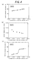
- Fig. 4(a), Fig. 4(b), and Fig. 4(c) show measurement results of the lateral breakdown voltage, the lateral leakage current, and the vertical breakdown voltage of Sample 4, respectively.
- the vertical breakdown voltage of Sample 4 was found to specifically increase steeply as the concentration of C in the portion of the main laminate on the buffer side exceeded 1 ⁇ 10 18 /cm 3 .
- the surface of each epitaxial substrate fabricated in the experiment example was observed under an optical microscope (100 power), and no cracks were found.
- Sample 7 was fabricated by a similar method to Sample 2 in Experiment Example 1 except that the initial growth layer was made of a GaN material (thickness: 20 nm) grown at 700 °C, and the growth temperature and pressure of each layer were set as shown in Table 3.
- Samples 8 to 10 were fabricated by similar methods to Samples 1 to 3 in Experiment Example 1 except that the initial growth layer was made of an Al 0.5 Ga 0.5 N material to perform the same experiments. As a result, each sample was found to have a similar result to Fig. 3(a), Fig. 3(b), and Fig. 3(c) , and to exhibit favorable characteristics such as a sheet resistance value of 450 ⁇ / ⁇ (square) or less and a mobility of 1550 cm 2 /Vs or more. The surface of each epitaxial substrate fabricated in the experiment example was observed under an optical microscope (100 power), and no cracks were found.
- Samples 11 to 13 were fabricated by similar methods to Samples 4 to 6 in Experiment Example 2 except that the initial growth layer was made of an Al 0.5 Ga 0.5 N material to perform the same experiments. As a result, each sample was found to have a similar result to Fig. 4(a), Fig. 4(b), and Fig. 4(c) . The surface of each epitaxial substrate fabricated in the experiment example was observed under an optical microscope (100 power), and no cracks were found.
- An epitaxial substrate for electronic devices includes a buffer having an Al-containing initial growth layer and a given superlattice laminate, and a given main laminate on a conductive SiC substrate; and the superlattice laminate and/or a portion of the main laminate on the buffer side has a C concentration of 1 ⁇ 10 18 /cm 3 or more.
Landscapes
- Junction Field-Effect Transistors (AREA)
- Crystals, And After-Treatments Of Crystals (AREA)
- Chemical Vapour Deposition (AREA)
Abstract
Description
- The present invention relates to an epitaxial substrate for electronic devices and a method of producing the same. The present invention specifically relates to an epitaxial substrate for HEMTs and a method of producing the same.
- In recent years, as speed required of IC devices and the like have increased, HEMTs (High electron mobility transistors) have been widely used as high-speed FETs (Field effect transistors). Such a field effect transistor is formed, as schematically illustrated in
FIG. 1 , for example by stacking achannel layer 22 and anelectron supply layer 23 on asubstrate 21 and then providing a surface of theelectron supply layer 23 with asource electrode 24, adrain electrode 25, and agate electrode 26. When the device is operated, electrons move through thesource electrode 24, theelectron supply layer 23, thechannel layer 22, theelectron supply layer 23, and thedrain electrode 25 in this order. A lateral direction is a current flow direction. This movement of electrons in the lateral direction, i.e. the current flow direction, is controlled by the voltage applied to thegate electrode 26. In HEMTs, electrons generated at a joint interface between theelectron supply layer 23 and thechannel layer 22 which have band gaps different from each other can move significantly fast, as compared with electrons in normal semiconductors. - As such, the movement of electrons, i.e. electric current in the lateral direction is controlled by the gate voltage. In general, although the gate voltage is turned OFF, the electric current is not brought to 0. The electric current which flows when the gate voltage is OFF is called leakage current. Increase of the leakage current increases power consumption, which would consequently cause problems of heat generation and the like. Such leakage current is generally divided into lateral leakage current and vertical leakage current. Lateral leakage current refers to leakage current that flows between two electrodes (for example, between the
source electrode 24 and the drain electrode 25) arranged on a surface on theelectron supply layer 23 side. Vertical leakage current refers to leakage current that flows between two electrodes separately arranged on a surface on theelectron supply layer 23 side and a surface on thesubstrate 21 side. - Now, to form an electronic device having a layered structure using a Group III nitride material, use of a SiC substrate is proposed, which is excellent in heat dissipation. Specifically, in order to suppress vertical leakage current and to improve breakdown voltage in the vertical direction at the same time, an insulating SiC substrate is generally used. However, it is difficult to make an insulating SiC substrate have higher resistance in manufacturing the substrate, which would increase the cost. Therefore, a method using a conductive SiC substrate is also proposed.
-
JP 2008-85123 (A - Further,
JP 2005-85852 (A - However, in the invention described in
JP 2008-85123 JP 2005-85852 - An object of the present invention is to provide an epitaxial substrate for electronic devices, in which a conductive SiC substrate is used as a substrate, both decrease in the lateral leakage current and improvement in the lateral breakdown voltage characteristics are successfully achieved, and the vertical breakdown voltage is improved, and besides, crack generation is suppressed; and a method of producing the same.
- In order to achieve the above object, the present invention primarily includes the following components.
- (1) An epitaxial substrate for an electronic device, comprising a conductive SiC single crystal substrate, a buffer as an insulating layer on the SiC single crystal substrate, and a main laminate formed by epitaxially growing a plurality of Group III nitride layers on the buffer, wherein a lateral direction is a current flow direction. The buffer includes at least an initial growth layer in contact with the SiC single crystal substrate and a superlattice laminate having a superlattice multi-layer structure on the initial growth layer. The initial growth layer is made of a Ba1Alb1Gac1Ind1N (0 ≤a1 ≤ 1, 0 < b1 ≤ 1, 0 ≤ c1 ≤ 1, 0 ≤ d1 < 1, a1 + b1 + c1 + d1 = 1) material. The superlattice laminate is configured by alternately stacking a first layer made of a Ba2Alb2Gac2Ind2N (0 ≤ a2 ≤1, 0 ≤ b2 ≤1, 0 ≤ c2 ≤ 1, 0 ≤ d2 ≤ 1, a2 + b2 + c2 + d2 = 1) material and a second layer made of a Ba3Alb3Gac3Ind3N (0 ≤ a3 ≤ 1, 0 ≤ b3 ≤ 1, 0 ≤ c3 ≤ 1, 0 ≤ d3 ≤ 1, a3 + b3 + c3 + d3 = 1) material having a different band gap from the first layer. Further, at least one of the superlattice laminate and a portion of the main laminate on the buffer side has a C concentration of 1 × 10¹⁸/cm3 or more.
- (2) The epitaxial substrate for an electronic device, according to (1) above, wherein both the superlattice laminate and the portion of the main laminate on the buffer side has a C concentration of 1 × 10¹⁸/cm3 or more.
- (3) The epitaxial substrate for an electronic device, according to (1) or (2) above, wherein the first layer is made of an AIN material, and the second layer is made of an Alb3Gac3N (a3 = 0, 0 < b3 ≤ 0.5, 0.5 ≤ c3 < 1, d3 = 0) material.
- (4) The epitaxial substrate for an electronic device, according to any one of (1) to (3) above, wherein the initial growth layer is made of a Ba1Alb1Gac1Ind1N (0 ≤ a1 ≤ 1, 0.5 ≤ b1 ≤ 1,0 ≤ c1 ≤ 1,0 ≤ d1 ≤ 1, a1 + b1 + c1 + d1 = 1) material.
- (5) The epitaxial substrate for an electronic device, according to any one of (1) to (3) above, wherein the initial growth layer is made of an AIN material.
- (6) A method of producing an epitaxial substrate for an electronic device, the epitaxial substrate comprising a conductive SiC single crystal substrate, a buffer as an insulating layer on the SiC single crystal substrate, and a main laminate formed by epitaxially growing a plurality of Group III nitride layers on the buffer, wherein a lateral direction is a current flow direction. The buffer includes at least an initial growth layer in contact with the SiC single crystal substrate and a superlattice laminate having a superlattice multi-layer structure on the initial growth layer. The initial growth layer is made of a Ba1Alb1Gac1Ind1N (0 ≤a1 ≤ 1, 0 < b1 ≤1, 0 ≤c1 ≤1, 0 ≤d1 ≤1, a1 + b1 + c1 + d1 = 1) material. The superlattice laminate is configured by alternately stacking a first layer made of a Ba2Alb2Gac2Ind2N (0 ≤ a2 ≤ 1, 0 ≤ b2 ≤1, 0 ≤ c2 ≤ 1, 0 ≤d2 ≤1, a2 + b2 + c2 + d2 = 1) material and a second layer made of a Ba3Alb3Gac3Ind3N (0 ≤a3 ≤1, 0 ≤b3 ≤ 1, 0 ≤ c3 ≤ 1, 0 ≤
d 3 1, a3 + b3 + c3 + d3 = 1) material having a different band gap from the first layer. Further, at least one of the superlattice laminate and a portion of the main laminate on the buffer side has a C concentration of 1 × 10¹⁸/cm3 or more. - (7) The method of producing the epitaxial substrate for an electronic device, according to (6) above, wherein both the superlattice laminate and the portion of the main laminate on the buffer side has a C concentration of 1 × 10¹⁸/cm3 or more.
- An epitaxial substrate for electronic devices according to the present invention includes a buffer having an initial growth layer made of an Al-containing Group III nitride and a given superlattice laminate, and a given main laminate, on a conductive SiC substrate. The superlattice laminate and/or a portion of the main laminate on the buffer side has a C concentration of 1 × 10¹⁸/cm3 or more, so that not only both decrease in the lateral leakage current and improvement in the lateral breakdown voltage characteristics are successfully achieved, but also vertical breakdown voltage can be improved. Moreover, use of the conductive SiC substrate can improve heat dissipation and reduce crack generation.
- Further, with a producing method according to the present invention, an epitaxial substrate for electronic devices, which includes a buffer having an initial growth layer made of an Al-containing Group III nitride and a given superlattice laminate, and a given main laminate, can be produced. The superlattice laminate and/or a portion of the main laminate on the buffer side has a C concentration of 1 × 10¹⁸/cm3 or more, so that not only both decrease in the lateral leakage current and improvement in the lateral breakdown voltage characteristics are successfully achieved, but also vertical breakdown voltage can be improved. Besides, use of a conductive SiC substrate can improve heat dissipation and reduce crack generation.
-
-
Fig. 1 is a schematic cross-sectional view illustrating a typical field effect transistor. -
Fig. 2 is a schematic cross-sectional view of an epitaxial substrate for electronic devices according to the present invention. -
Figs. 3(a), 3(b) and 3(c) are graphs showing measurement results of the lateral breakdown voltage, the lateral leakage current, and the vertical breakdown voltage, respectively. -
Figs. 4(a), 4(b) and 4(c) are graphs showing measurement results of the lateral breakdown voltage, the lateral leakage current, and the vertical breakdown voltage, respectively. - Next, an embodiment of an epitaxial substrate for electronic devices according to the present invention will be described with reference to the drawings.
Fig. 2 schematically shows a cross-section structure of an epitaxial substrate for electronic devices according to the present invention. Note that the epitaxial substrate inFig. 2 is enlarged in the thickness direction for the sake of explanation. - As shown in
Fig. 2 , anepitaxial substrate 1 for electronic devices according to the present invention has the following characteristic features. The lateral direction is a current flow direction. Theepitaxial substrate 1 comprises a conductive SiCsingle crystal substrate 2, abuffer 3 as an insulating layer formed on the conductive SiCsingle crystal substrate 2, and amain laminate 4 formed by epitaxially growing a plurality of Group III nitride layers on thebuffer 3. Thebuffer 3 at least includes aninitial growth layer 5 in contact with the Sisingle crystal substrate 2 and a superlattice laminate 6 having a superlattice multi-layer structure on theinitial growth layer 5. Theinitial growth layer 5 is made of a Ba1Alb1Gac1Ind1N (0 ≤ a1 ≤ 1, 0 < b1 ≤ 1, 0 ≤ c1 ≤ 1, 0 ≤ d1 ≤ 1, a1 + b1 + c1 + d1 = 1) material. In addition, the superlattice laminate 6 is formed by alternately stacking afirst layer 6a made of a Ba2Alb2Gac2Ind2N (0 ≤ a2 ≤ 1, 0 ≤ b2 ≤ 1, 0 ≤ c2 ≤1, 0 ≤ d2 ≤ 1, a2 + b2 + c2 + d2 = 1) material and asecond layer 6b made of a Ba3Alb3Gac3Ind3N (0 ≤ a3 ≤ 1, 0 ≤ b3 ≤ 1, 0 ≤ C3 ≤ 1, 0 ≤ d3 ≤ 1, a3 + b3 + C3 + d3 = 1) material having a different band gap from thefirst layer 6a. The superlattice laminate 6 and/or a portion 4' of themain laminate 4 on thebuffer 3 side has a C concentration of 1 × 10¹⁸/cm3 or more. With such a structure, not only both decrease in the lateral leakage current and improvement in the lateral breakdown voltage characteristics are successfully achieved, but also vertical breakdown voltage can be improved. Moreover, use of the conductive SiC substrate can improve heat dissipation and suppress crack generation. - Substrates having various crystal structures may be used for the conductive SiC
single crystal substrate 2; specifically, a 4H or 6H substrate is preferable. The crystal plane is not limited in particular, and (0001), (10-10), (11-20) planes and the like can be used. However, to grow the (0001) plane of a Group III nitride with good surface flatness, the (0001) plane is desirably used. Further, either p-type or n-type conductivity may be employed. With respect to the conductivity of the SiCsingle crystal substrate 2, a low resistance substrate having a resistivity of 1000 Ω·cm or less can be used as appropriate depending on the use. Note that SiC substrates having a resistivity of 1000 Ω·cm or less are herein referred to as conductive SiC substrates. Such a conductive SiCsingle crystal substrate 2 can be produced using various methods such as a sublimation method; alternatively, SiC can be homoepitaxially grown on a surface of a substrate. Further, a substrate having a surface provided with a thin film formed from an oxide film, a nitride film, or a carbide film can be used. Note that the reason that it is difficult to increase the resistivity of the SiC substrate is because nitrogen, which is the main constituent of air, easily contaminates the SiC substrate as an impurity, i.e. an n-type dopant, to reduce resistivity. - Further, the
initial growth layer 5 is formed of an Al-containing Group III nitride material (Ba1Alb1Gac1Ind1N (0 ≤ a1 ≤ 1, 0 < b1 ≤ 1, 0 ≤ c1 ≤ 1, 0 ≤ d1 ≤ 1, a1 + b1 + c1 + d1 = 1)), so that crack generation in an Al-containing superlattice laminate to be described later can be suppressed. In order to prevent cracks effectively, theinitial growth layer 5 preferably has higher Al composition than the layer which has the least Al composition in the superlattice laminate. In terms of the effect of preventing cracks, theinitial growth layer 5 is more preferably made of a Ba1Alb1Gac1Ind1N (0 ≤ a1 ≤ 1, 0.5 ≤ b1 ≤ 1, 0 ≤ c1 ≤ 1, 0 ≤ d1 ≤ 1, a1 + b1 + c1 + d1 = 1) material and most preferably made of an AIN. This is because the foregoing compositions can effectively suppress stretching stress in the superlattice laminate. Note that the A1N material here may include a minute amount of impurities of 1 % or less regardless of whether the inclusion was intended or not intended. For example, the AIN may include Ga or In above or other impurities such as Si, H, O, C, B, Mg, As, or P. The thickness of the initial growth layer is preferably within the range of 10 nm to 200 nm. When the initial layer is too thin, the stretching stress in the superlattice laminate cannot be fully suppressed, so cracks would occur in the superlattice laminate. When the initial layer is too thick, the stretching stress in the initial layer would accumulate to generate cracks in the initial layer. - Now, "the lateral direction is a current flow direction" refers to a state where, as illustrated in
Fig. 1 , electric current flows from thesource electrode 24 to thedrain electrode 25, mainly in the width direction of the laminate. This state is different from, for example, the state where electric current flows mainly in the vertical direction, that is, the direction of the thickness of the laminate as in a structure in which a semiconductor is sandwiched between a pair of electrodes. - Further, alternate stacking for forming the superlattice laminate here means to stack in such a way that the laminate cyclically includes the
first layer 6a and thesecond layer 6b. The laminate can include layers other than thefirst layer 6a and thesecond layer 6b (such as a compositional transition layer). - The concentration of C in the portion 4' of the
main laminate 4 on thebuffer 3 side is preferably higher than the concentration of C in the superlattice laminate 6. In the portion 4', due to the difference of the lattice constant between thebuffer 3 and themain laminate 4, a phenomenon in which dislocation bends in a lateral or oblique direction is observed, which forms a path allowing leakage current to flow easily. Therefore, leakage current flows more easily in the portion 4' than in thebuffer layer 3. To suppress this leakage current, the C concentration as described above is desired. Further, when the thickness of this portion 4' of themain laminate 4 on thebuffer 3 side is less than 0.1 µm, the dislocation would noticeably bend even in a portion with low C concentration. Therefore the thickness is preferably set to 0.1 µm or more. The upper limit of the thickness of the portion 4' is not specified in particular in terms of breakdown voltage improvement and reduction in leakage current, and it is set as appropriate in terms of reducing warpage and cracks of the substrate. - The
first layer 6a and thesecond layer 6b which constitute the superlattice laminate 6 are preferably made of an AIN material and an AlGaN (a3 = 0, 0 < b3 ≤ 0.5, 0.5 ≤ c3 < 1, d3 = 0) material, respectively. Since the band gap difference between thefirst layer 6a and thesecond layer 6b improves vertical breakdown voltage, the Al composition difference is preferably made as large as possible so that the band gap difference becomes as large as possible. When a mixed crystal is formed using a Group III nitride semiconductor material, AIN (6.2eV) and GaN (3.5eV) have the largest band gap difference; therefore, the superlattice structure is preferably formed from an AlGaN material. When the lower limit of the Al composition difference is less than 0.5, relaxation of stress due to lattice constant difference between Si single crystals and a Group III nitride is insufficient, which causes cracks; therefore, the composition difference is preferably 0.5 or more. Further, with respect to the upper limit of the composition difference, the Al composition difference is preferably large; however, it is desired that the second layer having a small band gap contains at least Al, and the Al composition difference is smaller than 1 since insulation of the AlGaN layer itself is promoted to improve breakdown voltage. This is because when the second layer contains at least Al, C can be efficiently introduced. Provided that the number of superlattice pairs is at least 40 pairs or more and the total film thickness is 1 µm or more, variation in breakdown voltage can be reduced, which is preferable. As this superlattice layer is thicker, the breakdown voltage can be increased, which is preferable for uses under high voltage. However, there is a disadvantage in that the material cost increases. Therefore, the thickness of the superlattice layer is selected as appropriate depending on the use. - With respect to the thickness of each layer in terms of improving breakdown voltage, the thickness of the
first layer 6a having a large band gap is preferably larger enough to suppress a tunnel current and is preferably smaller enough to prevent cracks. For example, when AIN is used, the thickness of thefirst layer 6a is preferably 2 nm to 10 nm. The thickness of thesecond layer 6b is set as appropriate in terms of suppressing cracks and controlling warpage. Preferably, the thickness of the layer having a relatively small band gap may be larger than that of the layer having a relatively large band gap to make the superlattice multilayer structure effectively demonstrate a strain-alleviating effect and suppress generation of cracks, and may be 40 nm or less. Further, the layers in the superlattice laminate are not necessarily stacked with the same film thickness, or the same composition. - The
epitaxial substrate 1 for electronic devices can be used for various uses where the lateral direction is the current flow direction. It is preferably used for HEMTs. Themain laminate 4 of theepitaxial substrate 1 shown inFig. 2 may include achannel layer 4a made of a Ba4Alb4Gac4Ind4N (0 ≤ a3 ≤1, 0 ≤ b3 ≤ 1, 0 ≤ c3 ≤ 1, 0 ≤ d3 ≤ 1, a3 + b3 + c3 + d3 = 1) material and anelectron supply layer 4b made of a Ba5Alb5Gac5lnd5N (0 ≤ a5 1, 0 ≤ b5 ≤ 1, 0 ≤ c5 ≤ 1, 0 ≤ d5 ≤ 1, a5 + b5 + c5 + d5 = 1) material having a larger band gap than thechannel layer 4a. On this occasion, either layer can be made of a single or a plurality of compositions. In particular, to prevent alloy scattering and to lower resistivity at the current flowing portion, at least a portion of thechannel layer 4a which is in contact with theelectron supply layer 4b is preferably made of a GaN material. - A portion of the
channel layer 4a on the side opposite to the buffer layer preferably has a low C concentration, and the concentration is preferably set at 4 × 10¹⁶/cm3 or less. This is because since this portion corresponds to the current flowing portion of an electronic device, it is preferable that the portion does not include impurities which hinder electrical conductivity or generate current collapse. Further, in order to suppress leakage owing to remaining carriers caused by n-type impurities, the C concentration is preferably 1 × 10¹⁵/cm3 or more. - Next, an embodiment of a producing method of an epitaxial substrate for electronic devices according to the present invention will be described with reference to the drawings.
- In a method of producing an
epitaxial substrate 1 for electronic devices, as shown inFig. 2 , abuffer 3 as an insulating layer and amain laminate 4 having a HEMT structure including a plurality of Group III nitride layers epitaxially grown on thebuffer 3 are formed in this order on a conductive SiCsingle crystal substrate 2, in which the lateral direction is a current flow direction. Theepitaxial substrate 1 is characteristically formed as follows. Thebuffer 3 includes aninitial growth layer 5 in contact with the SiCsingle crystal substrate 2 and a superlattice laminate 6 having a superlattice multi-layer structure on theinitial growth layer 5; theinitial growth layer 5 is made of a Ba1Alb1Gac1Ind1N (0 ≤ a1 ≤ 1,0 < b1 ≤ 1, 0 ≤ c1 ≤ 1, 0 ≤ d1 ≤ 1, a1 + b1 + c1 + d1 = 1) material; the superlattice laminate 6 is configured by alternately stacking afirst layer 6a made of a Ba2Alb2Gac2Ind2N (0 ≤ a2 ≤ 1, 0 ≤ b2 ≤ 1, 0 ≤ C2 ≤ 1, 0 ≤ d2 ≤ 1, a2 + b2 + c2 + d2 = 1) material and asecond layer 6b made of a Ba3Alb3Gac3Ind3N (0 ≤ a3 ≤ 1, 0 ≤ b3 ≤ 1, 0 ≤ c3 ≤ 1, 0 ≤ d3 ≤ 1, a3 + b3 + c3 + d3 = 1) material having a band gap different from thefirst layer 6a, and the superlattice laminate 6 and/or a portion 4' of the main laminate on thebuffer 3 side has a C concentration of 1 × 10¹⁸/cm3 or more. With such a structure, an epitaxial substrate for electronic devices can be manufactured in which vertical breakdown voltage characteristics and lateral breakdown voltage characteristics are both favorably achieved, and lateral leakage current can be reduced. The amounts of the other impurities are not limited in particular; however, intrusion of donor impurities (Si, O, Ge) having a relatively shallow impurity level is preferably suppressed. When C is contained as much as being able to compensate such a donor level, the intrusion of donor impurities is permitted to some extent. Note that with respect to the impurity concentration, while etching is performed from the surface side, the impurity concentration profile in the depth direction was measured using SIMS analysis. On this occasion, if the Group III element composition of only the portion 4' is modified, or the C concentration or the Group III element composition of a portion of thechannel layer 4a on the side opposite to the buffer layer is changed from the portion 4', the modification may be either abrupt or continuous. - C to be added to the superlattice laminate 6 and the portion 4' of the
main laminate 4 on thebuffer 3 side can be added by several methods shown below when the laminate is grown by CVD.
First method: A source gas containing C is additionally added during the growth of a Group III nitride. Methane, ethane, ethylene, acetylene, benzene, cyclopentane, and the like are given as examples.
Second method: A methyl group, an ethyl group, or the like in an organic metal is mixed into an epitaxial growth layer depending on the Group III nitride growth conditions. The growth temperature, growth pressure, growth rate; and the ammonia flow rate, hydrogen flow rate, or nitrogen flow rate at the time of growth; and the like are determined as appropriate so as to suppress decomposition of the organic metal; thus, the concentration of C to be added to the epitaxial growth layer can be controlled.
Note that, in the present invention, the concentration of C in the superlattice laminate 6 is a value measured by SIMS at a spot of the superlattice laminate 6 exposed after the half thickness of the superlattice laminate 6 is removed. The concentration of C in the portion 4' of themain laminate 4 on thebuffer 3 side is a value measured by SIMS at a spot of the portion 4' exposed after the half thickness of the portion 4' is removed. - Note that
Fig. 1 and Fig. 2 merely show examples of representative embodiments, and the present invention is not limited to these embodiments. For example, interlayers which would not adversely affect the effect of the present invention may be inserted or another superlattice layer may be inserted between each layer, or the composition may be graded. Further, a nitride film, a carbide film, an Al layer, or the like can be formed on the conductive SiC single crystal surface. - Note that the layered structure of the present invention can be applied not only to conductive SiC substrates, but also to other conductive substrates made of a variety of metal materials or low resistance semiconductor materials (such as Ge, GaN, AlGaN, GaAs, and ZnO) in which cracks generate if the initial growth layer is GaN. This can provide advantages of the present invention in that even when using a conductive substrate, crack generation can be suppressed, lateral leakage current is reduced, and breakdown voltage characteristics in the lateral direction and the vertical direction can be improved.
- On each of 300 µm-thick 3 inch 6H-SiC (0001) plane single crystal substrates having a resistivity of 1 × 10⁻¹ Ω·cm, 10 Ω·cm, and 100 Ω·cm, an initial growth layer (A1N material, thickness: 100 nm) and a superlattice laminate (A1N, film thickness: 4 nm and Al0.15Ga0.85N, film thickness: 25 nm, 85 layers in total) were grown to form a buffer. A channel layer (GaN material, thickness: 1.5 µm) and an electron supply layer (Al0.25Ga0.75N material, thickness: 20 nm) were epitaxially grown on the superlattice laminate to form a main laminate having a HEMT structure. Thus,
Samples 1 to 3 were obtained. The concentration of C in the superlattice laminate was changed, and the concentration of C in a portion of the main laminate on the buffer side was in the range of 1.5 × 10¹⁸/cm3 to 2.0 × 10¹⁸/cm3 in each result. Further, a portion of the channel layer on the electron supply layer side had a C concentration in the range of 0.8 × 10¹⁶/cm3 to 3.5 × 10¹⁶/cm3. The growth temperature and pressure of each layer are shown in Table 1. P1 in the table was controlled to control the C concentration, and the deposition pressure was reduced to increase the C concentration. MOCVD was used as a growth method. TMA (trimethylaluminium) and TMG (trimethylgallium) were used as Group III materials, and ammonia was used as a Group V material. Hydrogen gas and nitrogen gas were used as carrier gases. The deposition temperature here means a temperature of the substrate itself, measured during the growth using a radiation thermometer. Note that the SIMS measurement of the C concentration was performed by etching from the epitaxial layer side with a measuring apparatus manufactured by Cameca using Cs- as an ion source at an ion energy of 8 keV. -
Table 1 Layer Growth pressure (kPa) Growth temperature (°C) Initial growth layer 10 1025 Superlattice laminate P1 (1 - 120) 1025 Channel layer (buffer side) 10 1025 Channel layer (electron supply layer side) 100 1075 electron supply layer 10 1025 -
Fig. 3(a), Fig. 3(b), and Fig. 3(c) show measurement results of the lateral breakdown voltage, the lateral leakage current, and the vertical breakdown voltage ofSample 2, respectively. The measurement was performed as follows.
Vertical direction: a 80 µmϕ ohmic electrode having a Ti/Al layered structure was formed on the substrate surface, and the outside of the ohmic electrode was etched by a thickness of 50 nm. After that, the rear surface of the substrate was grounded to a metal plate, and the value of electric current flowing between the electrodes was measured with changing a voltage.
Lateral direction: 200 µm□ (square) two electrodes having a Ti/Al layered structure were formed to be arranged so that a side of each electrode was 10 µm distant from each other, and a portion around the ohmic electrodes was etched by a thickness of 150 nm. After that, the value of electric current flowing between the electrodes was measured with changing a voltage. On this occasion, to suppress electric discharge in the air, the electrodes were insulated from each other using an insulating oil. Further, for the purpose of avoiding the influence of leakage to the rear surface of the substrate, an insulating plate was placed under the substrate.
In this experiment example, the vertical breakdown voltage was defined as such a voltage value that a value obtained by converting the value of vertical current into the value per unit area by dividing by the electrode area amounts to 10-4A/cm2; the lateral breakdown voltage was defined as such a voltage value that a value obtained by converting the value of lateral current into the value per side length of the electrodes amounts to 10-4A/cm; and the lateral leakage current was defined as a value of current at a lateral voltage of 100 V between the two electrodes.
The concentration of C in the superlattice laminate 6 was obtained by measurement using SIMS, at a spot of the superlattice laminate 6 exposed after the half thickness of the superlattice laminate 6 is removed. The concentration of C in the portion 4' of themain laminate 4 on thebuffer 3 side was obtained by measurement using SIMS, at a spot of the portion 4' exposed after the half thickness of the portion 4' was removed. - As a result of changing the concentration of C in the superlattice laminate, the lateral breakdown voltage and the lateral leakage current did not almost change; however, the vertical breakdown voltage of
Sample 2 was found to specifically increase steeply as the concentration of C in the superlattice laminate exceeded 1 × 10¹⁸/cm3. Note thatSamples Fig. 3(a), Fig. 3(b), and Fig. 3(c) . - Note that as electrical characteristics of the channel layer portion in the epitaxial substrate fabricated in each experiment example were measured by Hall effect measurement, they were found to exhibit favorable characteristics such as a sheet resistance value of 440 Ω/□ (square) or less and a mobility of 1570 cm2/Vs or more.
The surface of each epitaxial substrate fabricated in the experiment example was observed under an optical microscope (100 power), and no cracks were found. -
Samples 4 to 6 were fabricated by similar methods toSamples 1 to 3 in Experiment Example 1 except that the growth pressure of the superlattice laminate was set at 10 kPa, the concentration of C in the portion of the main laminate on the buffer side was changed, and the growth temperature and pressure of each layer were set as shown in Table 2. P2 in the table was controlled to control the C concentration, and the deposition pressure was reduced to increase the C concentration. The concentration of C in the superlattice laminate was in the range of 1.5 × 10¹⁸/cm3 to 2.5 × 10¹⁸/cm3 in each result. -
Table 2 Layer Growth pressure (kPa) Growth temperature (°C) Initial growth layer 10 700 Superlattice laminate 10 1025 Channel layer (buffer side) P2 (1 - 120) 1025 Channel layer (electron supply layer side) 100 1075 electron supply layer 10 1025 -
Fig. 4(a), Fig. 4(b), and Fig. 4(c) show measurement results of the lateral breakdown voltage, the lateral leakage current, and the vertical breakdown voltage ofSample 4, respectively. As a result of changing the concentration of C in the main laminate, the lateral breakdown voltage and the lateral leakage current did not almost change; however, the vertical breakdown voltage ofSample 4 was found to specifically increase steeply as the concentration of C in the portion of the main laminate on the buffer side exceeded 1 × 10¹⁸/cm3. Further, as in Experiment Example 1 there was no significant difference found even inSamples 5 and 6 each using the Si single crystal substrate having a different resistivity, from the results shown inFigs. 4(a) to 4(c) .
The surface of each epitaxial substrate fabricated in the experiment example was observed under an optical microscope (100 power), and no cracks were found. - Experiment Examples 1 and 2 above indicate that when one of the concentration of C in the superlattice laminate and the concentration of C in the portion of the main laminate on the buffer side is set at 1 × 10¹⁸/cm3 or more, the vertical breakdown voltage can be increased effectively.
- Sample 7 was fabricated by a similar method to
Sample 2 in Experiment Example 1 except that the initial growth layer was made of a GaN material (thickness: 20 nm) grown at 700 °C, and the growth temperature and pressure of each layer were set as shown in Table 3. -
Table 3 Layer Growth pressure (kPa) Growth temperature (°C) Initial growth layer 10 700 Superlattice laminate P1 (1 - 120) 1025 Channel layer (buffer side) 10 1025 Channel layer (electron supply layer side) 100 1075 electron supply layer 10 1025 - When the surface of each epitaxial substrate fabricated in the experiment example was observed under an optical microscope (100 power), many cracks were found to generate. The cracks were generated in the entire surface of the wafer, which made it impossible to fabricate an experimental device.
- Samples 8 to 10 were fabricated by similar methods to
Samples 1 to 3 in Experiment Example 1 except that the initial growth layer was made of an Al0.5Ga0.5N material to perform the same experiments. As a result, each sample was found to have a similar result toFig. 3(a), Fig. 3(b), and Fig. 3(c) , and to exhibit favorable characteristics such as a sheet resistance value of 450 Ω/□ (square) or less and a mobility of 1550 cm2/Vs or more.
The surface of each epitaxial substrate fabricated in the experiment example was observed under an optical microscope (100 power), and no cracks were found. - Samples 11 to 13 were fabricated by similar methods to
Samples 4 to 6 in Experiment Example 2 except that the initial growth layer was made of an Al0.5Ga0.5N material to perform the same experiments. As a result, each sample was found to have a similar result toFig. 4(a), Fig. 4(b), and Fig. 4(c) .
The surface of each epitaxial substrate fabricated in the experiment example was observed under an optical microscope (100 power), and no cracks were found. - An epitaxial substrate for electronic devices according to the present invention includes a buffer having an Al-containing initial growth layer and a given superlattice laminate, and a given main laminate on a conductive SiC substrate; and the superlattice laminate and/or a portion of the main laminate on the buffer side has a C concentration of 1 × 10¹⁸/cm3 or more. Thus, not only both decrease in the lateral leakage current and improvement in the lateral breakdown voltage characteristics are successfully achieved, but also vertical breakdown voltage can be improved. Moreover, use of the conductive SiC substrate can improve heat dissipation and reduce crack generation.
-
- 1: Epitaxial substrate for electronic devices
- 2: Conductive SiC single crystal substrate
- 3: Buffer
- 4: Main laminate
- 4a: Channel layer
- 4b: Electron supply layer
- 5: Initial growth layer
- 6: Superlattice laminate
- 6a: First layer
- 6b: Second layer
Claims (7)
- An epitaxial substrate for an electronic device, comprising:a conductive SiC single crystal substrate,a buffer as an insulating layer on the SiC single crystal substrate, anda main laminate formed by epitaxially growing a plurality of Group III nitride layers on the buffer,wherein a lateral direction is a current flow direction,
the buffer includes at least an initial growth layer in contact with the SiC single crystal substrate and a superlattice laminate having a superlattice multi-layer structure on the initial growth layer,
the initial growth layer is made of a Ba1Alb1Gac1Ind1N (0 ≤ a1 ≤ 1, 0 < b1 ≤ 1, 0 ≤ c1 ≤ 1, 0 ≤ d1 ≤ 1, a1 + b1 + c1 +d1 = 1)material,
the superlattice laminate is configured by alternately stacking a first layer made of a Ba2Alb2Gac2Ind2N (0 ≤a2 ≤ 1, 0 ≤b2 ≤ 1,0 ≤ c2 ≤ 1,0 ≤ d2 ≤ 1, a2 +b2 + c2 + d2 =1) material and a second layer made of a Ba3Alb3Gac3Ind3N (0 ≤ a3 ≤ 1, 0 ≤ b3 ≤ 1, 0 ≤ c3 ≤ 1, 0 ≤ d3 ≤ 1, a3 + b3 + c3 + d3 = 1) material having a different band gap from the first layer, and
at least one of the superlattice laminate and a portion of the main laminate on the buffer side has a C concentration of 1 × 10¹⁸/cm3 or more. - The epitaxial substrate for an electronic device, according to claim 1,
wherein both the superlattice laminate and the portion of the main laminate on the buffer side has a C concentration of 1 × 10¹⁸/cm3 or more. - The epitaxial substrate for an electronic device, according to claim 1 or claim 2,
wherein the first layer is made of an AIN material, and the second layer is made of an Alb3Gac3N (a3 = 0, 0 < b3 ≤ 0.5, 0.5 ≤ c3 < 1, d3 = 0) material. - The epitaxial substrate for an electronic device, according to any one of claims 1 to 3,
wherein the initial growth layer is made of a Ba1Alb1Gac1Ind1N (0 ≤ a1 ≤ 1, 0.5 ≤ b1 ≤ 1,0 ≤ c1 ≤ 1, 0 ≤ d1 ≤ 1, a1 + b1 + c1 + d1 = 1) material. - The epitaxial substrate for an electronic device, according to any one of claims 1 to 3,
wherein the initial growth layer is made of an AIN material. - A method of producing an epitaxial substrate for an electronic device, the epitaxial substrate comprising:a conductive SiC single crystal substrate,a buffer as an insulating layer on the SiC single crystal substrate, anda main laminate formed by epitaxially growing a plurality of Group III nitride layers on the buffer,wherein a lateral direction is a current flow direction,
the buffer includes at least an initial growth layer in contact with the SiC single crystal substrate and a superlattice laminate having a superlattice multi-layer structure on the initial growth layer,
the initial growth layer is made of a Ba1Alb1Gac1Ind1N (0 ≤ a1 ≤ 1, 0 < b1 ≤ 1, 0 ≤ c1 ≤ 1,0 ≤d1 ≤ 1,a1 + b1 + c1 + d1 = 1)material,
the superlattice laminate is configured by alternately stacking a first layer made of a Ba2Alb2Gac2Ind2N (0 ≤ a2 ≤ 1, 0 ≤ b2 ≤ 1, 0 ≤ c2 ≤ 1, 0 ≤ d2 ≤ 1, a2 + b2 + C2 + d2 = 1) material and a second layer made of a Ba3Alb3Gac3Ind3N (0 ≤ a3 ≤ 1, 0 ≤ b3 ≤ 1, 0 ≤ c3 ≤ 1, 0 ≤ d3 ≤ 1, a3 + b3 + c3 + d3 = 1) material having a different band gap from the first layer, and
at least one of the superlattice laminate and a portion of the main laminate on the buffer side has a C concentration of 1 × 10¹⁸/cm3 or more. - The method of producing the epitaxial substrate for an electronic device, according to claim 6,
wherein both the superlattice laminate and the portion of the main laminate on the buffer side each has a C concentration of 1 × 10¹⁸/cm3 or more.
Applications Claiming Priority (3)
| Application Number | Priority Date | Filing Date | Title |
|---|---|---|---|
| JP2009114860 | 2009-05-11 | ||
| JP2010107821A JP4685961B2 (en) | 2009-05-11 | 2010-05-10 | Epitaxial substrate for electronic device and manufacturing method thereof |
| PCT/JP2010/003162 WO2010131451A1 (en) | 2009-05-11 | 2010-05-10 | Epitaxial substrate for electronic device and process for producing same |
Publications (2)
| Publication Number | Publication Date |
|---|---|
| EP2432005A1 true EP2432005A1 (en) | 2012-03-21 |
| EP2432005A4 EP2432005A4 (en) | 2015-05-27 |
Family
ID=43084836
Family Applications (1)
| Application Number | Title | Priority Date | Filing Date |
|---|---|---|---|
| EP10774710.7A Withdrawn EP2432005A4 (en) | 2009-05-11 | 2010-05-10 | EPITAXIAL SUBSTRATE FOR ELECTRONIC DEVICE AND ITS PRODUCTION PROCESS |
Country Status (7)
| Country | Link |
|---|---|
| US (1) | US8426893B2 (en) |
| EP (1) | EP2432005A4 (en) |
| JP (1) | JP4685961B2 (en) |
| KR (1) | KR101321625B1 (en) |
| CN (1) | CN102460664B (en) |
| TW (1) | TWI466290B (en) |
| WO (1) | WO2010131451A1 (en) |
Cited By (1)
| Publication number | Priority date | Publication date | Assignee | Title |
|---|---|---|---|---|
| AT521082A3 (en) * | 2013-07-30 | 2020-01-15 | Sumitomo Chemical Co | Semiconductor wafer and method for manufacturing the semiconductor wafer |
Families Citing this family (23)
| Publication number | Priority date | Publication date | Assignee | Title |
|---|---|---|---|---|
| EP2498282A4 (en) * | 2009-11-04 | 2014-06-25 | Dowa Electronics Materials Co Ltd | NITRIDE III SUBSTRATE WITH EPITAXIAL STRATIFICATION |
| JP5514920B2 (en) * | 2012-01-13 | 2014-06-04 | Dowaエレクトロニクス株式会社 | Group III nitride epitaxial substrate and deep ultraviolet light emitting device using the substrate |
| JP5228122B1 (en) * | 2012-03-08 | 2013-07-03 | 株式会社東芝 | Nitride semiconductor device and nitride semiconductor wafer |
| CN102969341A (en) * | 2012-11-09 | 2013-03-13 | 中国电子科技集团公司第五十五研究所 | Nitride High Electron Mobility Transistor Epitaxial Structure with Gradient AlyGa1-yN Buffer Layer |
| JP5787417B2 (en) * | 2013-05-14 | 2015-09-30 | コバレントマテリアル株式会社 | Nitride semiconductor substrate |
| JP2015053328A (en) * | 2013-09-05 | 2015-03-19 | 富士通株式会社 | Semiconductor device |
| US9159788B2 (en) | 2013-12-31 | 2015-10-13 | Industrial Technology Research Institute | Nitride semiconductor structure |
| CN106415802B (en) * | 2014-05-26 | 2019-07-02 | 夏普株式会社 | Nitride-based compound semiconductors |
| WO2015181648A1 (en) | 2014-05-27 | 2015-12-03 | The Silanna Group Pty Limited | An optoelectronic device |
| US11322643B2 (en) | 2014-05-27 | 2022-05-03 | Silanna UV Technologies Pte Ltd | Optoelectronic device |
| KR102318317B1 (en) | 2014-05-27 | 2021-10-28 | 실라나 유브이 테크놀로지스 피티이 리미티드 | Advanced electronic device structures using semiconductor structures and superlattices |
| WO2015181656A1 (en) | 2014-05-27 | 2015-12-03 | The Silanna Group Pty Limited | Electronic devices comprising n-type and p-type superlattices |
| US9608103B2 (en) * | 2014-10-02 | 2017-03-28 | Toshiba Corporation | High electron mobility transistor with periodically carbon doped gallium nitride |
| WO2016072521A1 (en) * | 2014-11-07 | 2016-05-12 | 住友化学株式会社 | Semiconductor substrate and method for inspecting semiconductor substrate |
| US11335799B2 (en) * | 2015-03-26 | 2022-05-17 | Chih-Shu Huang | Group-III nitride semiconductor device and method for fabricating the same |
| WO2016155794A1 (en) | 2015-03-31 | 2016-10-06 | Erik Janzén | Heterostructure and method of its production |
| JP6615075B2 (en) * | 2016-09-15 | 2019-12-04 | サンケン電気株式会社 | Semiconductor device substrate, semiconductor device, and method for manufacturing semiconductor device substrate |
| JP6796467B2 (en) * | 2016-11-30 | 2020-12-09 | 住友化学株式会社 | Semiconductor substrate |
| JP6376257B2 (en) * | 2017-09-01 | 2018-08-22 | 富士通株式会社 | Semiconductor device |
| CN112750904B (en) | 2019-10-30 | 2024-01-02 | 联华电子股份有限公司 | Semiconductor component with stress relaxation layer |
| JP7654367B2 (en) * | 2020-08-24 | 2025-04-01 | エア・ウォーター株式会社 | Compound semiconductor substrate and compound semiconductor device |
| US12482653B2 (en) * | 2020-09-30 | 2025-11-25 | Dynax Semiconductor, Inc. | Epitaxial structure of semiconductor device and method of manufacturing the same |
| TWI818379B (en) * | 2021-12-08 | 2023-10-11 | 財團法人工業技術研究院 | High electron mobility transistor device |
Family Cites Families (16)
| Publication number | Priority date | Publication date | Assignee | Title |
|---|---|---|---|---|
| KR100398514B1 (en) * | 1997-01-09 | 2003-09-19 | 니치아 카가쿠 고교 가부시키가이샤 | Nitride Semiconductor Device |
| JP3946969B2 (en) | 2001-05-31 | 2007-07-18 | 日本碍子株式会社 | Field effect transistor and heterojunction bipolar transistor |
| US7030428B2 (en) | 2001-12-03 | 2006-04-18 | Cree, Inc. | Strain balanced nitride heterojunction transistors |
| US6995473B2 (en) * | 2002-12-19 | 2006-02-07 | Matsushita Electric Industrial Co., Ltd. | Stacked semiconductor transistors |
| JP4530171B2 (en) * | 2003-08-08 | 2010-08-25 | サンケン電気株式会社 | Semiconductor device |
| JP4509031B2 (en) * | 2003-09-05 | 2010-07-21 | サンケン電気株式会社 | Nitride semiconductor device |
| JP3960957B2 (en) | 2003-09-05 | 2007-08-15 | 古河電気工業株式会社 | Semiconductor electronic device |
| JP2006114655A (en) | 2004-10-14 | 2006-04-27 | Hitachi Cable Ltd | Semiconductor epitaxial wafer and field effect transistor |
| JP4542912B2 (en) * | 2005-02-02 | 2010-09-15 | 株式会社東芝 | Nitrogen compound semiconductor device |
| US7491626B2 (en) * | 2005-06-20 | 2009-02-17 | Sensor Electronic Technology, Inc. | Layer growth using metal film and/or islands |
| JP2007214384A (en) * | 2006-02-09 | 2007-08-23 | Rohm Co Ltd | Nitride semiconductor device |
| JP5064824B2 (en) * | 2006-02-20 | 2012-10-31 | 古河電気工業株式会社 | Semiconductor element |
| WO2008012877A1 (en) * | 2006-07-26 | 2008-01-31 | Fujitsu Limited | COMPOUND SEMICONDUCTOR DEVICE EMPLOYING SiC SUBSTRATE AND PROCESS FOR PRODUCING THE SAME |
| JP2008085123A (en) | 2006-09-28 | 2008-04-10 | Covalent Materials Corp | Compound semiconductor device substrate and compound semiconductor device using the same |
| JP5224311B2 (en) * | 2007-01-05 | 2013-07-03 | 古河電気工業株式会社 | Semiconductor electronic device |
| KR20090119849A (en) * | 2007-02-16 | 2009-11-20 | 스미또모 가가꾸 가부시키가이샤 | Gallium nitride based epitaxial crystals, a method of manufacturing the same and a field effect transistor |
-
2010
- 2010-05-10 WO PCT/JP2010/003162 patent/WO2010131451A1/en not_active Ceased
- 2010-05-10 JP JP2010107821A patent/JP4685961B2/en active Active
- 2010-05-10 US US13/319,910 patent/US8426893B2/en active Active
- 2010-05-10 EP EP10774710.7A patent/EP2432005A4/en not_active Withdrawn
- 2010-05-10 CN CN201080031291.0A patent/CN102460664B/en active Active
- 2010-05-10 KR KR1020117029263A patent/KR101321625B1/en active Active
- 2010-05-11 TW TW099114928A patent/TWI466290B/en active
Non-Patent Citations (1)
| Title |
|---|
| See references of WO2010131451A1 * |
Cited By (1)
| Publication number | Priority date | Publication date | Assignee | Title |
|---|---|---|---|---|
| AT521082A3 (en) * | 2013-07-30 | 2020-01-15 | Sumitomo Chemical Co | Semiconductor wafer and method for manufacturing the semiconductor wafer |
Also Published As
| Publication number | Publication date |
|---|---|
| TWI466290B (en) | 2014-12-21 |
| KR20120023761A (en) | 2012-03-13 |
| US8426893B2 (en) | 2013-04-23 |
| EP2432005A4 (en) | 2015-05-27 |
| JP4685961B2 (en) | 2011-05-18 |
| US20120091435A1 (en) | 2012-04-19 |
| TW201101486A (en) | 2011-01-01 |
| CN102460664A (en) | 2012-05-16 |
| JP2010287882A (en) | 2010-12-24 |
| KR101321625B1 (en) | 2013-10-23 |
| WO2010131451A1 (en) | 2010-11-18 |
| CN102460664B (en) | 2014-08-13 |
Similar Documents
| Publication | Publication Date | Title |
|---|---|---|
| US8426893B2 (en) | Epitaxial substrate for electronic device and method of producing the same | |
| EP2360719B1 (en) | Epitaxial substrate for electronic devices and manufacturing method therefor | |
| US9685323B2 (en) | Buffer layer structures suited for III-nitride devices with foreign substrates | |
| US8847203B2 (en) | Group III nitride epitaxial laminate substrate | |
| US8946863B2 (en) | Epitaxial substrate for electronic device comprising a high resistance single crystal substrate on a low resistance single crystal substrate, and method of manufacturing | |
| US10388517B2 (en) | Epitaxial substrate for electronic device and method of producing the same | |
| JP5787417B2 (en) | Nitride semiconductor substrate | |
| US20140209862A1 (en) | Group iii nitride epitaxial substrate and method for manufacturing the same | |
| US8785942B2 (en) | Nitride semiconductor substrate and method of manufacturing the same | |
| EP2565906A1 (en) | Epitaxial substrate and process for producing epitaxial substrate | |
| EP2565928A1 (en) | Epitaxial substrate and method for producing epitaxial substrate | |
| EP2290696B1 (en) | Epitaxial substrate for semiconductor device, semiconductor device, and method of manufacturing epitaxial substrate for semiconductor device | |
| EP2455964A1 (en) | Epitaxial substrate for electronic device using transverse direction as direction of current conduction and manufacturing method therefor | |
| US20190157081A1 (en) | Method for Forming a Semiconductor Structure for a Gallium Nitride Channel Device | |
| CN103314429A (en) | Layer structures for controlling stress of heteroepitaxially grown III-nitride layers | |
| JP2015070085A (en) | Epitaxial substrate for electronic device and manufacturing method thereof | |
| JP2015070091A (en) | Group iii nitride semiconductor substrate | |
| JP2011258782A (en) | Nitride semiconductor substrate | |
| JP6404738B2 (en) | EPITAXIAL SUBSTRATE FOR ELECTRONIC DEVICE, HIGH ELECTRON MOBILITY TRANSISTOR, AND METHOD FOR PRODUCING THEM |
Legal Events
| Date | Code | Title | Description |
|---|---|---|---|
| PUAI | Public reference made under article 153(3) epc to a published international application that has entered the european phase |
Free format text: ORIGINAL CODE: 0009012 |
|
| 17P | Request for examination filed |
Effective date: 20111117 |
|
| AK | Designated contracting states |
Kind code of ref document: A1 Designated state(s): AL AT BE BG CH CY CZ DE DK EE ES FI FR GB GR HR HU IE IS IT LI LT LU LV MC MK MT NL NO PL PT RO SE SI SK SM TR |
|
| DAX | Request for extension of the european patent (deleted) | ||
| RA4 | Supplementary search report drawn up and despatched (corrected) |
Effective date: 20150424 |
|
| RIC1 | Information provided on ipc code assigned before grant |
Ipc: H01L 29/15 20060101ALI20150420BHEP Ipc: H01L 29/207 20060101ALI20150420BHEP Ipc: H01L 29/20 20060101ALI20150420BHEP Ipc: H01L 29/778 20060101AFI20150420BHEP |
|
| STAA | Information on the status of an ep patent application or granted ep patent |
Free format text: STATUS: THE APPLICATION IS DEEMED TO BE WITHDRAWN |
|
| 18D | Application deemed to be withdrawn |
Effective date: 20151124 |