EP2432003A2 - Silicon Carbide Semiconductor Device - Google Patents
Silicon Carbide Semiconductor Device Download PDFInfo
- Publication number
- EP2432003A2 EP2432003A2 EP11181275A EP11181275A EP2432003A2 EP 2432003 A2 EP2432003 A2 EP 2432003A2 EP 11181275 A EP11181275 A EP 11181275A EP 11181275 A EP11181275 A EP 11181275A EP 2432003 A2 EP2432003 A2 EP 2432003A2
- Authority
- EP
- European Patent Office
- Prior art keywords
- layer
- sic
- semiconductor device
- silicon carbide
- interface
- Prior art date
- Legal status (The legal status is an assumption and is not a legal conclusion. Google has not performed a legal analysis and makes no representation as to the accuracy of the status listed.)
- Withdrawn
Links
Images



Classifications
-
- H—ELECTRICITY
- H10—SEMICONDUCTOR DEVICES; ELECTRIC SOLID-STATE DEVICES NOT OTHERWISE PROVIDED FOR
- H10D—INORGANIC ELECTRIC SEMICONDUCTOR DEVICES
- H10D30/00—Field-effect transistors [FET]
- H10D30/60—Insulated-gate field-effect transistors [IGFET]
- H10D30/64—Double-diffused metal-oxide semiconductor [DMOS] FETs
- H10D30/66—Vertical DMOS [VDMOS] FETs
-
- H—ELECTRICITY
- H10—SEMICONDUCTOR DEVICES; ELECTRIC SOLID-STATE DEVICES NOT OTHERWISE PROVIDED FOR
- H10P—GENERIC PROCESSES OR APPARATUS FOR THE MANUFACTURE OR TREATMENT OF DEVICES COVERED BY CLASS H10
- H10P14/00—Formation of materials, e.g. in the shape of layers or pillars
- H10P14/20—Formation of materials, e.g. in the shape of layers or pillars of semiconductor materials
- H10P14/29—Formation of materials, e.g. in the shape of layers or pillars of semiconductor materials characterised by the substrates
- H10P14/2901—Materials
- H10P14/2902—Materials being Group IVA materials
- H10P14/2904—Silicon carbide
-
- H—ELECTRICITY
- H10—SEMICONDUCTOR DEVICES; ELECTRIC SOLID-STATE DEVICES NOT OTHERWISE PROVIDED FOR
- H10D—INORGANIC ELECTRIC SEMICONDUCTOR DEVICES
- H10D30/00—Field-effect transistors [FET]
- H10D30/60—Insulated-gate field-effect transistors [IGFET]
- H10D30/67—Thin-film transistors [TFT]
- H10D30/674—Thin-film transistors [TFT] characterised by the active materials
- H10D30/6741—Group IV materials, e.g. germanium or silicon carbide
-
- H—ELECTRICITY
- H10—SEMICONDUCTOR DEVICES; ELECTRIC SOLID-STATE DEVICES NOT OTHERWISE PROVIDED FOR
- H10D—INORGANIC ELECTRIC SEMICONDUCTOR DEVICES
- H10D62/00—Semiconductor bodies, or regions thereof, of devices having potential barriers
- H10D62/80—Semiconductor bodies, or regions thereof, of devices having potential barriers characterised by the materials
- H10D62/83—Semiconductor bodies, or regions thereof, of devices having potential barriers characterised by the materials being Group IV materials, e.g. B-doped Si or undoped Ge
- H10D62/832—Semiconductor bodies, or regions thereof, of devices having potential barriers characterised by the materials being Group IV materials, e.g. B-doped Si or undoped Ge being Group IV materials comprising two or more elements, e.g. SiGe
- H10D62/8325—Silicon carbide
-
- H—ELECTRICITY
- H10—SEMICONDUCTOR DEVICES; ELECTRIC SOLID-STATE DEVICES NOT OTHERWISE PROVIDED FOR
- H10D—INORGANIC ELECTRIC SEMICONDUCTOR DEVICES
- H10D64/00—Electrodes of devices having potential barriers
- H10D64/01—Manufacture or treatment
- H10D64/013—Manufacture or treatment of electrodes having a conductor capacitively coupled to a semiconductor by an insulator
- H10D64/01366—Manufacture or treatment of electrodes having a conductor capacitively coupled to a semiconductor by an insulator the semiconductor being silicon carbide
-
- H—ELECTRICITY
- H10—SEMICONDUCTOR DEVICES; ELECTRIC SOLID-STATE DEVICES NOT OTHERWISE PROVIDED FOR
- H10D—INORGANIC ELECTRIC SEMICONDUCTOR DEVICES
- H10D84/00—Integrated devices formed in or on semiconductor substrates that comprise only semiconducting layers, e.g. on Si wafers or on GaAs-on-Si wafers
- H10D84/01—Manufacture or treatment
- H10D84/0123—Integrating together multiple components covered by H10D12/00 or H10D30/00, e.g. integrating multiple IGBTs
-
- H—ELECTRICITY
- H10—SEMICONDUCTOR DEVICES; ELECTRIC SOLID-STATE DEVICES NOT OTHERWISE PROVIDED FOR
- H10D—INORGANIC ELECTRIC SEMICONDUCTOR DEVICES
- H10D84/00—Integrated devices formed in or on semiconductor substrates that comprise only semiconducting layers, e.g. on Si wafers or on GaAs-on-Si wafers
- H10D84/01—Manufacture or treatment
- H10D84/02—Manufacture or treatment characterised by using material-based technologies
- H10D84/03—Manufacture or treatment characterised by using material-based technologies using Group IV technology, e.g. silicon technology or silicon-carbide [SiC] technology
- H10D84/038—Manufacture or treatment characterised by using material-based technologies using Group IV technology, e.g. silicon technology or silicon-carbide [SiC] technology using silicon technology, e.g. SiGe
-
- H—ELECTRICITY
- H10—SEMICONDUCTOR DEVICES; ELECTRIC SOLID-STATE DEVICES NOT OTHERWISE PROVIDED FOR
- H10P—GENERIC PROCESSES OR APPARATUS FOR THE MANUFACTURE OR TREATMENT OF DEVICES COVERED BY CLASS H10
- H10P14/00—Formation of materials, e.g. in the shape of layers or pillars
- H10P14/20—Formation of materials, e.g. in the shape of layers or pillars of semiconductor materials
- H10P14/32—Formation of materials, e.g. in the shape of layers or pillars of semiconductor materials characterised by intermediate layers between substrates and deposited layers
- H10P14/3202—Materials thereof
- H10P14/3204—Materials thereof being Group IVA semiconducting materials
- H10P14/3208—Silicon carbide
-
- H—ELECTRICITY
- H10—SEMICONDUCTOR DEVICES; ELECTRIC SOLID-STATE DEVICES NOT OTHERWISE PROVIDED FOR
- H10P—GENERIC PROCESSES OR APPARATUS FOR THE MANUFACTURE OR TREATMENT OF DEVICES COVERED BY CLASS H10
- H10P14/00—Formation of materials, e.g. in the shape of layers or pillars
- H10P14/20—Formation of materials, e.g. in the shape of layers or pillars of semiconductor materials
- H10P14/34—Deposited materials, e.g. layers
- H10P14/3402—Deposited materials, e.g. layers characterised by the chemical composition
- H10P14/3404—Deposited materials, e.g. layers characterised by the chemical composition being Group IVA materials
- H10P14/3408—Silicon carbide
-
- H—ELECTRICITY
- H10—SEMICONDUCTOR DEVICES; ELECTRIC SOLID-STATE DEVICES NOT OTHERWISE PROVIDED FOR
- H10P—GENERIC PROCESSES OR APPARATUS FOR THE MANUFACTURE OR TREATMENT OF DEVICES COVERED BY CLASS H10
- H10P10/00—Bonding of wafers, substrates or parts of devices
- H10P10/12—Bonding of semiconductor wafers or semiconductor substrates to semiconductor wafers or semiconductor substrates
- H10P10/128—Bonding of semiconductor wafers or semiconductor substrates to semiconductor wafers or semiconductor substrates by direct semiconductor to semiconductor bonding
Definitions
- the invention relates to semiconductor devices manufactured with silicon carbide and methods of manufacturing such devices.
- One particular application of the invention is in the manufacture of MOSFETs (metal-oxide-semiconductor field effect transistors) using silicon carbide.
- MOSFETs metal-oxide-semiconductor field effect transistors
- the invention also relates to aircraft power distribution systems that utilise such MOSFETs.
- SiC silicon carbide
- MOSFET MOSFET
- the channel region lies beneath the oxide layer at the gate of the MOSFET, and when the MOSFET is switched on the channel region allows the flow of current through the device.
- Previous attempts to produce SiC MOSFETs have been subject to the problem of carbon gettering at the interface, whereby carbon impurities are formed at the interface, adversely affecting the electrical behaviour of the device.
- US5,744,826 discloses a process for producing silicon carbide semiconductor devices, such as MOSFETs, wherein a gate insulating film is formed on the surface of a SiC semiconductor layer, by thermal oxidation of the SiC layer.
- the present invention provides a method of manufacturing a semiconductor device comprising applying a first layer comprising silicon to a second layer comprising silicon carbide, whereby an interface is defined between the first and second layers, and oxidising some or all of the first layer.
- the quality of each surface of the first and second layers can be independently ensured, thereby resulting in high quality of each surface, and especially the interface between the layers. Further, as this process does not oxidise any SiC, the problems associated with carbon gettering at the interface are overcome. Thus the interface provided by the present invention is of high quality. Naturally, great care is needed in the preparation of the SiC layer as high levels of cleanliness and flatness are desired.
- Wafer bonding can be used to attach the first and second layers to one another.
- wafer bonding a thin layer of single crystal silicon is transferred from a carrier wafer on to the surface of another target wafer, in this case the SiC layer.
- the transferred layer is of high quality, so it can be oxidised to form an oxide of correspondingly high quality.
- the present invention provides a semiconductor device manufactured according to the above described method comprising a first layer comprising SiO 2 joined to a second layer comprising silicon carbide, whereby an interface is defined between the first and second layers. Additionally, the invention provides an aircraft power distribution system including such a semiconductor device.
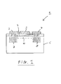
- Fig. 1 shows a basic structure of a prior art field effect transistor 1, such as a MOSFET, which comprises a source 2, a drain 4 and a gate 3, each of which includes an electrically conductive contact.
- a layer 9 of an electrical insulator such as an oxide, for example silicon dioxide, is provided between the source 2, the drain 4, the gate 3 and a substrate 5. Adjacent to the layer 9, when the MOSFET is switched on by applying a potential to the gate 3, a conductive channel 10 is formed in the substrate 5, allowing current to flow between the source 2 and the drain 4.
- the substrate 5 comprises a p-type material and the source 2 includes a first region 7 of n-type material, whilst the drain 4 includes a second region 8 of n-type material.
- a positive electrical potential is applied to the gate 3, thereby attracting negative charge carriers towards the nonconductive layer 9, and if the applied potential exceeds the threshold for switching the device on, a channel 10 of essentially n-type material is formed.
- a continuous conduction path of n-type material is thereby provided between the source 2 and the drain 4 allowing current to flow therebetween.
- the present invention is also applicable to p-channel MOSFETs wherein the p-type and n-type materials are arranged in an opposite configuration to that just described. In general terms, the invention is applicable to any type of MOSFET, or other semiconductor devices which require an interface between a semiconducting layer and an insulating layer.
- Fig. 2 is a cross-sectional view illustrating the problem with oxidising SiC directly.
- the oxidation of SiC generally produces a layer of SiO 2 12 on top of the layer of SiC 11 that is being oxidised.
- Other non-stoichiometric oxides of silicon may be present in the SiO 2 layer 12.
- Carbon clusters 13 are formed at an interface 14 between the SiC layer 11 and the SiO 2 layer 12, to the detriment of the electrical properties of the arrangement.
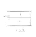
- Fig. 3 is a cross-sectional view of part of a semiconductor device embodying the invention, comprising a first layer 16 of SiO 2 disposed on a second layer 15 of SiC. No carbon clusters are present at the interface 17, because the device was manufactured according to the method of the invention.
- Figures 4A, 4B, 4C and 4D are cross-sectional views showing the stages of a method embodying the invention. As shown in Fig. 4A , the starting point is a layer of SiC 15.
- a layer 18 of Si is wafer bonded to the layer of SiC 15.
- the wafer bonded layer 18 of Si is oxidised. Oxygen reacts with the Si layer 18 from its outer surface 20 inwards, wherein an at least partially oxidised layer 18 of Si is formed.
- the degree of oxidation of the layer 18 can be controlled for example by performing the oxidation for a predetermined time at a known oxidation rate.
- the oxidation can be carried out at a temperature great enough to oxidise Si but not to oxidise SiC. This ensures that no oxidation of the SiC layer 15 takes place.
- the oxidation can be continued until the Si layer is fully oxidised.
- a layer of unoxidised Si may be left between the SiC and the oxidised layer of Si, by terminating the oxidation before the Si layer is fully oxidised.
- Fig. 4D shows the arrangement of layers after the oxidation process is completed, wherein a layer 16 of SiO 2 is provided on the layer 15 of SiC.
- the SiO 2 layer 16 is etched away in regions 26,27 shown in Fig 5 , to expose first and second regions 23,25 of heavily doped n-type SiC and first and second regions 22,24 of doped p-type SiC in the SiC layer 15.
- the regions 22 to 25 are not shown in Figs 4A to 4D .
- the rest of the SiC layer 15 comprises moderately doped n-type SiC, and in particular can consist of a single crystal of SiC.
- a source contact (not shown) is provided in the regions 26 and 27, whilst a drain contact 23 is provided on the opposite side of the device.
- a layer 22 of heavily doped n-type SiC is provided between the SiC layer 15 and the drain contact 23.
- the gate electrode 21 is provided on the layer 16 of SiO 2 .
- the contacts can be made of any good electrical conductor, for example Nickel.
- SiC MOSFETs embodying the present invention are particularly suited for use in aircraft power distribution systems.
- the issue of aircraft wiring safety has received widespread attention in recent years. Both "smoke in the cockpit" and arcing events are relevant here, and efforts are being made to improve the safety of such systems.
- Aircraft electric power systems are exposed to a wide range of disturbances, which may initiate such events. These include current and voltage transients and short-circuit conditions, arising from equipment failure and lightning strikes, for example.
- Electro-mechanical circuit breakers have traditionally been used to protect against such faults; however many of the faults are below the time protection curve threshold designed to protect the power system.
- SSPC's Solid State Power Controllers
- SSPCs Solid State Power Controllers
- electro-mechanical controllers can replace electro-mechanical controllers and provide improved performance, including very fast response, limiting the fault current within safe limits, and a long multi-operation life span. They further allow a flexible construction and control scheme, being fully controllable for both functions of current limiting and interruption.
- SSPCs also are of low cost and require minimal maintenance.
- MOSFETs have a very low on-state resistance, allowing a low voltage drop and hence a small power dissipation (as heat) during operation.
- a plurality of MOSFETs may have to be placed in parallel to enable the devices to withstand the associated energy losses.
- the steady-state cooling requirements i.e. size, mass and heat transfer, are defined by normal operation, and (2) the number of devices in parallel is defined by fault conditions; in this case the high power dissipation levels will not act for long enough to heat up the external contact to the devices (i.e.
- MOSFET devices manufactured using SiC as provided by the present invention provide a solution to this problem as they have a much smaller on-state resistance than corresponding Si devices. Improved sensitivity to fault currents can thereby be provided, as well as reduced I 2 R heating.
- Silicon carbide is also a much better thermal conductor and has a higher melting/sublimation temperature than Si and so is able to run hotter, thus reducing the requirement for heavy heatsink arrangements. Together, the material advantages of silicon carbide allow much higher power densities to be achieved.
Landscapes
- Insulated Gate Type Field-Effect Transistor (AREA)
- Chemical & Material Sciences (AREA)
- Crystallography & Structural Chemistry (AREA)
- Electrodes Of Semiconductors (AREA)
- Carbon And Carbon Compounds (AREA)
- Formation Of Insulating Films (AREA)
Abstract

Description
- The invention relates to semiconductor devices manufactured with silicon carbide and methods of manufacturing such devices. One particular application of the invention is in the manufacture of MOSFETs (metal-oxide-semiconductor field effect transistors) using silicon carbide. The invention also relates to aircraft power distribution systems that utilise such MOSFETs.
- The use of silicon carbide, SiC, in the manufacture of MOSFETs provides a number of benefits over traditional silicon substrates. For example, SiC has very high strength and does not melt at any known pressure and is chemically highly stable. Further, SiC allows the production of devices having a lower on-state resistance than silicon devices. Thus SiC lends itself to use in high power MOSFETs.
- One problem associated with the manufacture of MOSFETS using SiC is that it has not been possible to make a channel region of the MOSFET with high enough quality to produce viable devices that are sufficiently reliable for practical use. In a MOSFET, the channel region lies beneath the oxide layer at the gate of the MOSFET, and when the MOSFET is switched on the channel region allows the flow of current through the device. Previous attempts to produce SiC MOSFETs have been subject to the problem of carbon gettering at the interface, whereby carbon impurities are formed at the interface, adversely affecting the electrical behaviour of the device.
-
US5,744,826 discloses a process for producing silicon carbide semiconductor devices, such as MOSFETs, wherein a gate insulating film is formed on the surface of a SiC semiconductor layer, by thermal oxidation of the SiC layer. - In order to provide the required electrical properties in the channel region, it is important that a good quality interface is defined between the oxide and the SiC beneath it. The present invention provides a method of manufacturing a semiconductor device comprising applying a first layer comprising silicon to a second layer comprising silicon carbide, whereby an interface is defined between the first and second layers, and oxidising some or all of the first layer.
- By virtue of applying the first layer comprising silicon to the second layer comprising SiC, the quality of each surface of the first and second layers can be independently ensured, thereby resulting in high quality of each surface, and especially the interface between the layers. Further, as this process does not oxidise any SiC, the problems associated with carbon gettering at the interface are overcome. Thus the interface provided by the present invention is of high quality. Naturally, great care is needed in the preparation of the SiC layer as high levels of cleanliness and flatness are desired.
- Wafer bonding can be used to attach the first and second layers to one another. In wafer bonding, a thin layer of single crystal silicon is transferred from a carrier wafer on to the surface of another target wafer, in this case the SiC layer. The transferred layer is of high quality, so it can be oxidised to form an oxide of correspondingly high quality.
- Further, the present invention provides a semiconductor device manufactured according to the above described method comprising a first layer comprising SiO2 joined to a second layer comprising silicon carbide, whereby an interface is defined between the first and second layers. Additionally, the invention provides an aircraft power distribution system including such a semiconductor device.
- There follows a detailed description of embodiments of the invention by way of example only with reference to the accompanying drawings, in which:
-
Fig.1 is a schematic simplified view of a field effect transistor such as a MOSFET; -
Fig.2 is a cross-sectional view illustrating the problem of carbon gettering; -
Fig. 3 illustrates an arrangement of layers according to an embodiment of the invention; -
Figs 4A, 4B, 4C and 4D illustrate the stages of a process according to an embodiment of the invention; and -
Fig. 5 illustrates a further stage in a process according to an embodiment of the invention. -
Fig. 1 shows a basic structure of a prior artfield effect transistor 1, such as a MOSFET, which comprises asource 2, adrain 4 and agate 3, each of which includes an electrically conductive contact. A layer 9 of an electrical insulator such as an oxide, for example silicon dioxide, is provided between thesource 2, thedrain 4, thegate 3 and a substrate 5. Adjacent to the layer 9, when the MOSFET is switched on by applying a potential to thegate 3, aconductive channel 10 is formed in the substrate 5, allowing current to flow between thesource 2 and thedrain 4. In an n-channel MOSFET, the substrate 5 comprises a p-type material and thesource 2 includes afirst region 7 of n-type material, whilst thedrain 4 includes asecond region 8 of n-type material. In order to switch on the n-channel MOSFET, a positive electrical potential is applied to thegate 3, thereby attracting negative charge carriers towards the nonconductive layer 9, and if the applied potential exceeds the threshold for switching the device on, achannel 10 of essentially n-type material is formed. A continuous conduction path of n-type material is thereby provided between thesource 2 and thedrain 4 allowing current to flow therebetween. Upon removal of the potential at thegate 3, the charge carrier distribution within the substrate 5 reverts to its normal state, thereby removing theconductive channel 10 and switching the device off. The present invention is also applicable to p-channel MOSFETs wherein the p-type and n-type materials are arranged in an opposite configuration to that just described. In general terms, the invention is applicable to any type of MOSFET, or other semiconductor devices which require an interface between a semiconducting layer and an insulating layer. -
Fig. 2 is a cross-sectional view illustrating the problem with oxidising SiC directly. Depending on reaction conditions, the oxidation of SiC generally produces a layer ofSiO 2 12 on top of the layer of SiC 11 that is being oxidised. Other non-stoichiometric oxides of silicon may be present in the SiO2 layer 12.Carbon clusters 13 are formed at aninterface 14 between the SiC layer 11 and the SiO2 layer 12, to the detriment of the electrical properties of the arrangement. -
Fig. 3 is a cross-sectional view of part of a semiconductor device embodying the invention, comprising afirst layer 16 of SiO2 disposed on asecond layer 15 of SiC. No carbon clusters are present at theinterface 17, because the device was manufactured according to the method of the invention. -
Figures 4A, 4B, 4C and 4D are cross-sectional views showing the stages of a method embodying the invention. As shown inFig. 4A , the starting point is a layer ofSiC 15. - In
Fig. 4B , alayer 18 of Si is wafer bonded to the layer ofSiC 15. InFig. 4C , the wafer bondedlayer 18 of Si is oxidised. Oxygen reacts with theSi layer 18 from itsouter surface 20 inwards, wherein an at least partially oxidisedlayer 18 of Si is formed. The degree of oxidation of thelayer 18 can be controlled for example by performing the oxidation for a predetermined time at a known oxidation rate. - Alternatively or additionally, the oxidation can be carried out at a temperature great enough to oxidise Si but not to oxidise SiC. This ensures that no oxidation of the
SiC layer 15 takes place. The oxidation can be continued until the Si layer is fully oxidised. Alternatively, a layer of unoxidised Si may be left between the SiC and the oxidised layer of Si, by terminating the oxidation before the Si layer is fully oxidised. - This provides another way of ensuring that the layer of SiC is not oxidised during the process.
Fig. 4D shows the arrangement of layers after the oxidation process is completed, wherein alayer 16 of SiO2 is provided on thelayer 15 of SiC. - Following the completion of the oxidation process, the SiO2 layer 16 is etched away in
regions Fig 5 , to expose first andsecond regions second regions SiC layer 15. For simplicity theregions 22 to 25 are not shown inFigs 4A to 4D . The rest of theSiC layer 15 comprises moderately doped n-type SiC, and in particular can consist of a single crystal of SiC. A source contact (not shown) is provided in theregions drain contact 23 is provided on the opposite side of the device. Alayer 22 of heavily doped n-type SiC is provided between theSiC layer 15 and thedrain contact 23. Thegate electrode 21 is provided on thelayer 16 of SiO2. The contacts can be made of any good electrical conductor, for example Nickel. - SiC MOSFETs embodying the present invention are particularly suited for use in aircraft power distribution systems. The issue of aircraft wiring safety has received widespread attention in recent years. Both "smoke in the cockpit" and arcing events are relevant here, and efforts are being made to improve the safety of such systems. Aircraft electric power systems are exposed to a wide range of disturbances, which may initiate such events. These include current and voltage transients and short-circuit conditions, arising from equipment failure and lightning strikes, for example. Electro-mechanical circuit breakers have traditionally been used to protect against such faults; however many of the faults are below the time protection curve threshold designed to protect the power system.
- SSPC's (Solid State Power Controllers) can replace electro-mechanical controllers and provide improved performance, including very fast response, limiting the fault current within safe limits, and a long multi-operation life span. They further allow a flexible construction and control scheme, being fully controllable for both functions of current limiting and interruption. SSPCs also are of low cost and require minimal maintenance.
- Generally, MOSFETs have a very low on-state resistance, allowing a low voltage drop and hence a small power dissipation (as heat) during operation. However, in order to be able to withstand the short-circuit or fault current for the designated time, a plurality of MOSFETs may have to be placed in parallel to enable the devices to withstand the associated energy losses. There are two principal constraints in action: (1) The steady-state cooling requirements, i.e. size, mass and heat transfer, are defined by normal operation, and (2) the number of devices in parallel is defined by fault conditions; in this case the high power dissipation levels will not act for long enough to heat up the external contact to the devices (i.e. the case), due to the short time of action and the diffusion of heat from the semiconductor device itself to the case. In other words, if there are not enough SSPCs provided in the system, excessive heating can occur during fault conditions. Reducing the number of parallel MOSFETs, and thus giving improvements in size and mass, would be acceptable for normal operation; however this would not allow the fault conditions to be safely contained. MOSFET devices manufactured using SiC as provided by the present invention provide a solution to this problem as they have a much smaller on-state resistance than corresponding Si devices. Improved sensitivity to fault currents can thereby be provided, as well as reduced I2R heating. Silicon carbide is also a much better thermal conductor and has a higher melting/sublimation temperature than Si and so is able to run hotter, thus reducing the requirement for heavy heatsink arrangements. Together, the material advantages of silicon carbide allow much higher power densities to be achieved.
Claims (10)
- A method of manufacturing a semiconductor device comprising applying a first layer comprising silicon to a second layer comprising silicon carbide, whereby an interface is defined between the first and second layers, and oxidising some or all of the first layer.
- A method according to claim 1, wherein the first layer is wafer bonded to the second layer.
- A method according to claim 1 or 2, wherein the second layer consists of a single crystal of SiC.
- A method according to any of the preceding claims, wherein the first layer consists of a single crystal of Si.
- A method according to any of claims 1 to 4, wherein the step of oxidising some or all of the first layer is carried out after the first layer is applied to the second layer.
- A method according to any of claims 1 to 4, wherein the step of oxidising some or all of the first layer is carried out before or while the first layer is applied to the second layer.
- A semiconductor device manufactured in accordance with the method of any of claim 1 to 6, comprising a first layer comprising SiO2 joined to a second layer comprising silicon carbide, whereby an interface is defined between the first and second layers.
- A semiconductor device according to claim 7 comprising a MOSFET.
- An aircraft power distribution system comprising a semiconductor device according to claim 7 or 8.
- A method of manufacturing a semiconductor device substantially as herein described with reference to the accompanying drawings.
Applications Claiming Priority (1)
| Application Number | Priority Date | Filing Date | Title |
|---|---|---|---|
| GB1015595.0A GB2483702A (en) | 2010-09-17 | 2010-09-17 | Method for the manufacture of a Silicon Carbide, Silicon Oxide interface having reduced interfacial carbon gettering |
Publications (2)
| Publication Number | Publication Date |
|---|---|
| EP2432003A2 true EP2432003A2 (en) | 2012-03-21 |
| EP2432003A3 EP2432003A3 (en) | 2012-08-08 |
Family
ID=43065408
Family Applications (1)
| Application Number | Title | Priority Date | Filing Date |
|---|---|---|---|
| EP11181275A Withdrawn EP2432003A3 (en) | 2010-09-17 | 2011-09-14 | Silicon Carbide Semiconductor Device |
Country Status (7)
| Country | Link |
|---|---|
| US (1) | US20120068194A1 (en) |
| EP (1) | EP2432003A3 (en) |
| JP (1) | JP2012074696A (en) |
| CN (1) | CN102412300A (en) |
| BR (1) | BRPI1103938A2 (en) |
| CA (1) | CA2751927A1 (en) |
| GB (1) | GB2483702A (en) |
Families Citing this family (2)
| Publication number | Priority date | Publication date | Assignee | Title |
|---|---|---|---|---|
| JP7253730B2 (en) * | 2018-12-26 | 2023-04-07 | 株式会社日進製作所 | Semiconductor device manufacturing method and semiconductor device |
| WO2021005683A1 (en) * | 2019-07-08 | 2021-01-14 | 株式会社Fuji | Circuit pattern creating system, and method for creating circuit pattern |
Citations (1)
| Publication number | Priority date | Publication date | Assignee | Title |
|---|---|---|---|---|
| US5744826A (en) | 1996-01-23 | 1998-04-28 | Denso Corporation | Silicon carbide semiconductor device and process for its production |
Family Cites Families (26)
| Publication number | Priority date | Publication date | Assignee | Title |
|---|---|---|---|---|
| US5272107A (en) * | 1983-09-24 | 1993-12-21 | Sharp Kabushiki Kaisha | Manufacture of silicon carbide (SiC) metal oxide semiconductor (MOS) device |
| JPS6066866A (en) * | 1983-09-24 | 1985-04-17 | Sharp Corp | Manufacture of silicon carbide mos structure |
| JP2560765B2 (en) * | 1988-01-20 | 1996-12-04 | 富士通株式会社 | Large area semiconductor substrate manufacturing method |
| US5459107A (en) * | 1992-06-05 | 1995-10-17 | Cree Research, Inc. | Method of obtaining high quality silicon dioxide passivation on silicon carbide and resulting passivated structures |
| IT1268123B1 (en) * | 1994-10-13 | 1997-02-20 | Sgs Thomson Microelectronics | SLICE OF SEMICONDUCTOR MATERIAL FOR THE MANUFACTURE OF INTEGRATED DEVICES AND PROCEDURE FOR ITS MANUFACTURING. |
| US6171931B1 (en) * | 1994-12-15 | 2001-01-09 | Sgs-Thomson Microelectronics S.R.L. | Wafer of semiconductor material for fabricating integrated devices, and process for its fabrication |
| SE9700215L (en) * | 1997-01-27 | 1998-02-18 | Abb Research Ltd | Process for producing a SiC semiconductor layer of the 3C polytype on top of a semiconductor substrate layer utilizes the wafer bonding technique |
| FR2801723B1 (en) * | 1999-11-25 | 2003-09-05 | Commissariat Energie Atomique | HIGHLY OXYGEN-SENSITIVE SILICON LAYER AND METHOD FOR OBTAINING THE LAYER |
| JP4325095B2 (en) * | 2000-09-08 | 2009-09-02 | 株式会社デンソー | Manufacturing method of SiC element |
| US6689669B2 (en) * | 2001-11-03 | 2004-02-10 | Kulite Semiconductor Products, Inc. | High temperature sensors utilizing doping controlled, dielectrically isolated beta silicon carbide (SiC) sensing elements on a specifically selected high temperature force collecting membrane |
| US6593209B2 (en) * | 2001-11-15 | 2003-07-15 | Kulite Semiconductor Products, Inc. | Closing of micropipes in silicon carbide (SiC) using oxidized polysilicon techniques |
| JP4100070B2 (en) * | 2002-07-05 | 2008-06-11 | トヨタ自動車株式会社 | Manufacturing method of semiconductor device |
| US7122488B2 (en) * | 2004-03-15 | 2006-10-17 | Sharp Laboratories Of America, Inc. | High density plasma process for the formation of silicon dioxide on silicon carbide substrates |
| US20040245571A1 (en) * | 2003-02-13 | 2004-12-09 | Zhiyuan Cheng | Semiconductor-on-insulator article and method of making same |
| DE60336543D1 (en) * | 2003-05-27 | 2011-05-12 | Soitec Silicon On Insulator | Process for producing a heteroepitaxial microstructure |
| US7560361B2 (en) * | 2004-08-12 | 2009-07-14 | International Business Machines Corporation | Method of forming gate stack for semiconductor electronic device |
| DE602006020027D1 (en) * | 2005-02-16 | 2011-03-24 | Leach Int Corp | POWER DISTRIBUTION SYSTEM USING SOLID BODY CONTROLLERS |
| US7749863B1 (en) * | 2005-05-12 | 2010-07-06 | Hrl Laboratories, Llc | Thermal management substrates |
| FR2888398B1 (en) * | 2005-07-05 | 2007-12-21 | Commissariat Energie Atomique | HIGHLY OXYGEN-SENSITIVE SILICON LAYER AND METHOD OF OBTAINING THE LAYER |
| US7977821B2 (en) * | 2007-05-10 | 2011-07-12 | Honeywell International Inc. | High power density switch module with improved thermal management and packaging |
| JP2009088440A (en) * | 2007-10-03 | 2009-04-23 | Oki Semiconductor Co Ltd | Semiconductor device and manufacturing method thereof |
| JP4700045B2 (en) * | 2007-11-13 | 2011-06-15 | Okiセミコンダクタ株式会社 | Manufacturing method of semiconductor device |
| JP4844609B2 (en) * | 2008-09-25 | 2011-12-28 | 富士電機株式会社 | Method for forming oxide film on silicon carbide semiconductor substrate |
| JP2010251724A (en) * | 2009-03-26 | 2010-11-04 | Semiconductor Energy Lab Co Ltd | Method for manufacturing semiconductor substrate |
| US9018077B2 (en) * | 2009-04-30 | 2015-04-28 | Arizona Board Of Regents, A Body Corporate Of The State Of Arizona, Acting For And On Behalf Of Arizona State University | Methods for wafer bonding, and for nucleating bonding nanophases |
| US8193848B2 (en) * | 2009-06-02 | 2012-06-05 | Cree, Inc. | Power switching devices having controllable surge current capabilities |
-
2010
- 2010-09-17 GB GB1015595.0A patent/GB2483702A/en not_active Withdrawn
-
2011
- 2011-09-05 BR BRPI1103938-8A patent/BRPI1103938A2/en not_active Application Discontinuation
- 2011-09-08 CA CA2751927A patent/CA2751927A1/en not_active Abandoned
- 2011-09-14 EP EP11181275A patent/EP2432003A3/en not_active Withdrawn
- 2011-09-15 US US13/233,146 patent/US20120068194A1/en not_active Abandoned
- 2011-09-15 CN CN2011102835030A patent/CN102412300A/en active Pending
- 2011-09-16 JP JP2011202686A patent/JP2012074696A/en not_active Withdrawn
Patent Citations (1)
| Publication number | Priority date | Publication date | Assignee | Title |
|---|---|---|---|---|
| US5744826A (en) | 1996-01-23 | 1998-04-28 | Denso Corporation | Silicon carbide semiconductor device and process for its production |
Also Published As
| Publication number | Publication date |
|---|---|
| CN102412300A (en) | 2012-04-11 |
| GB201015595D0 (en) | 2010-10-27 |
| GB2483702A8 (en) | 2012-04-04 |
| JP2012074696A (en) | 2012-04-12 |
| US20120068194A1 (en) | 2012-03-22 |
| CA2751927A1 (en) | 2012-03-17 |
| GB2483702A (en) | 2012-03-21 |
| BRPI1103938A2 (en) | 2013-01-15 |
| EP2432003A3 (en) | 2012-08-08 |
Similar Documents
| Publication | Publication Date | Title |
|---|---|---|
| WO2013042406A1 (en) | Electric power semiconductor device | |
| JPWO2011007387A1 (en) | Power semiconductor device and manufacturing method thereof | |
| JP2022159154A (en) | Power semiconductor device, package structure and electronic device | |
| CN107395171B (en) | Monolithically integrated semiconductor switches, especially power disconnect switches | |
| US5844273A (en) | Vertical semiconductor device and method of manufacturing the same | |
| CN114342089B (en) | Silicon carbide semiconductor device and power conversion device | |
| CN102412305B (en) | Power-insulated-gate field-effect transistor | |
| EP3474330B1 (en) | Lateral insulated-gate bipolar transistor and manufacturing method therefor | |
| JP2012033731A (en) | Power semiconductor device | |
| US11929420B2 (en) | Power semiconductor devices having multilayer gate dielectric layers that include an etch stop/field control layer and methods of forming such devices | |
| KR20130020629A (en) | Presspin, power semiconducter module and semiconducter module assembly with multiple power semiconducter modules | |
| US20120068194A1 (en) | Silicon carbide semiconductor devices | |
| JPH0691244B2 (en) | Gate turn-off thyristor manufacturing method | |
| JP2009021395A (en) | Semiconductor device | |
| US5831291A (en) | Insulated gate bipolar transistors | |
| US20230420527A1 (en) | Gate trench power semiconductor devices having improved breakdown performance and methods of forming such devices | |
| CN113644133B (en) | Semiconductor device and preparation method thereof | |
| JPH04274368A (en) | Insulated gate type bipolar transistor and manufacture thereof | |
| US10325984B2 (en) | Monolithically integrated semiconductor switch, in particular a power circuit breaker | |
| CN214672630U (en) | Novel high-voltage groove grid MOS device | |
| CN102215039B (en) | For the power switch of aircraft | |
| JP2009055200A (en) | Control device and control method for silicon carbide static induction transistor | |
| CN102280483A (en) | Power device with side stage protecting source and gate and manufacture method thereof | |
| CN121240492A (en) | Groove type SiC MOSFET and preparation method thereof | |
| CN119855206A (en) | Terminal structure, manufacturing method thereof, semiconductor device, power module and vehicle |
Legal Events
| Date | Code | Title | Description |
|---|---|---|---|
| PUAI | Public reference made under article 153(3) epc to a published international application that has entered the european phase |
Free format text: ORIGINAL CODE: 0009012 |
|
| AK | Designated contracting states |
Kind code of ref document: A2 Designated state(s): AL AT BE BG CH CY CZ DE DK EE ES FI FR GB GR HR HU IE IS IT LI LT LU LV MC MK MT NL NO PL PT RO RS SE SI SK SM TR |
|
| AX | Request for extension of the european patent |
Extension state: BA ME |
|
| PUAL | Search report despatched |
Free format text: ORIGINAL CODE: 0009013 |
|
| AK | Designated contracting states |
Kind code of ref document: A3 Designated state(s): AL AT BE BG CH CY CZ DE DK EE ES FI FR GB GR HR HU IE IS IT LI LT LU LV MC MK MT NL NO PL PT RO RS SE SI SK SM TR |
|
| AX | Request for extension of the european patent |
Extension state: BA ME |
|
| RIC1 | Information provided on ipc code assigned before grant |
Ipc: H01L 29/78 20060101ALN20120702BHEP Ipc: H01L 29/16 20060101ALN20120702BHEP Ipc: H01L 21/28 20060101AFI20120702BHEP Ipc: H03K 17/082 20060101ALN20120702BHEP Ipc: H01L 21/18 20060101ALN20120702BHEP |
|
| 17P | Request for examination filed |
Effective date: 20130208 |
|
| 17Q | First examination report despatched |
Effective date: 20130411 |
|
| STAA | Information on the status of an ep patent application or granted ep patent |
Free format text: STATUS: THE APPLICATION IS DEEMED TO BE WITHDRAWN |
|
| 18D | Application deemed to be withdrawn |
Effective date: 20131022 |